EP1895229A1 - Surface illuminator - Google Patents
Surface illuminator Download PDFInfo
- Publication number
- EP1895229A1 EP1895229A1 EP06757128A EP06757128A EP1895229A1 EP 1895229 A1 EP1895229 A1 EP 1895229A1 EP 06757128 A EP06757128 A EP 06757128A EP 06757128 A EP06757128 A EP 06757128A EP 1895229 A1 EP1895229 A1 EP 1895229A1
- Authority
- EP
- European Patent Office
- Prior art keywords
- light source
- fpc
- point
- hole
- conductor pattern
- Prior art date
- Legal status (The legal status is an assumption and is not a legal conclusion. Google has not performed a legal analysis and makes no representation as to the accuracy of the status listed.)
- Withdrawn
Links
Images

Classifications
-
- G—PHYSICS
- G02—OPTICS
- G02B—OPTICAL ELEMENTS, SYSTEMS OR APPARATUS
- G02B6/00—Light guides; Structural details of arrangements comprising light guides and other optical elements, e.g. couplings
- G02B6/0001—Light guides; Structural details of arrangements comprising light guides and other optical elements, e.g. couplings specially adapted for lighting devices or systems
- G02B6/0011—Light guides; Structural details of arrangements comprising light guides and other optical elements, e.g. couplings specially adapted for lighting devices or systems the light guides being planar or of plate-like form
- G02B6/0081—Mechanical or electrical aspects of the light guide and light source in the lighting device peculiar to the adaptation to planar light guides, e.g. concerning packaging
- G02B6/0085—Means for removing heat created by the light source from the package
-
- H—ELECTRICITY
- H05—ELECTRIC TECHNIQUES NOT OTHERWISE PROVIDED FOR
- H05K—PRINTED CIRCUITS; CASINGS OR CONSTRUCTIONAL DETAILS OF ELECTRIC APPARATUS; MANUFACTURE OF ASSEMBLAGES OF ELECTRICAL COMPONENTS
- H05K1/00—Printed circuits
- H05K1/02—Details
- H05K1/0201—Thermal arrangements, e.g. for cooling, heating or preventing overheating
- H05K1/0203—Cooling of mounted components
- H05K1/0204—Cooling of mounted components using means for thermal conduction connection in the thickness direction of the substrate
- H05K1/0206—Cooling of mounted components using means for thermal conduction connection in the thickness direction of the substrate by printed thermal vias
-
- H—ELECTRICITY
- H05—ELECTRIC TECHNIQUES NOT OTHERWISE PROVIDED FOR
- H05K—PRINTED CIRCUITS; CASINGS OR CONSTRUCTIONAL DETAILS OF ELECTRIC APPARATUS; MANUFACTURE OF ASSEMBLAGES OF ELECTRICAL COMPONENTS
- H05K2201/00—Indexing scheme relating to printed circuits covered by H05K1/00
- H05K2201/02—Fillers; Particles; Fibers; Reinforcement materials
- H05K2201/0203—Fillers and particles
- H05K2201/0206—Materials
- H05K2201/0209—Inorganic, non-metallic particles
-
- H—ELECTRICITY
- H05—ELECTRIC TECHNIQUES NOT OTHERWISE PROVIDED FOR
- H05K—PRINTED CIRCUITS; CASINGS OR CONSTRUCTIONAL DETAILS OF ELECTRIC APPARATUS; MANUFACTURE OF ASSEMBLAGES OF ELECTRICAL COMPONENTS
- H05K2201/00—Indexing scheme relating to printed circuits covered by H05K1/00
- H05K2201/09—Shape and layout
- H05K2201/09209—Shape and layout details of conductors
- H05K2201/09372—Pads and lands
- H05K2201/09481—Via in pad; Pad over filled via
-
- H—ELECTRICITY
- H05—ELECTRIC TECHNIQUES NOT OTHERWISE PROVIDED FOR
- H05K—PRINTED CIRCUITS; CASINGS OR CONSTRUCTIONAL DETAILS OF ELECTRIC APPARATUS; MANUFACTURE OF ASSEMBLAGES OF ELECTRICAL COMPONENTS
- H05K2201/00—Indexing scheme relating to printed circuits covered by H05K1/00
- H05K2201/09—Shape and layout
- H05K2201/09209—Shape and layout details of conductors
- H05K2201/095—Conductive through-holes or vias
- H05K2201/0959—Plated through-holes or plated blind vias filled with insulating material
-
- H—ELECTRICITY
- H05—ELECTRIC TECHNIQUES NOT OTHERWISE PROVIDED FOR
- H05K—PRINTED CIRCUITS; CASINGS OR CONSTRUCTIONAL DETAILS OF ELECTRIC APPARATUS; MANUFACTURE OF ASSEMBLAGES OF ELECTRICAL COMPONENTS
- H05K2201/00—Indexing scheme relating to printed circuits covered by H05K1/00
- H05K2201/10—Details of components or other objects attached to or integrated in a printed circuit board
- H05K2201/10007—Types of components
- H05K2201/10106—Light emitting diode [LED]
-
- H—ELECTRICITY
- H05—ELECTRIC TECHNIQUES NOT OTHERWISE PROVIDED FOR
- H05K—PRINTED CIRCUITS; CASINGS OR CONSTRUCTIONAL DETAILS OF ELECTRIC APPARATUS; MANUFACTURE OF ASSEMBLAGES OF ELECTRICAL COMPONENTS
- H05K3/00—Apparatus or processes for manufacturing printed circuits
- H05K3/0058—Laminating printed circuit boards onto other substrates, e.g. metallic substrates
- H05K3/0061—Laminating printed circuit boards onto other substrates, e.g. metallic substrates onto a metallic substrate, e.g. a heat sink
-
- H—ELECTRICITY
- H05—ELECTRIC TECHNIQUES NOT OTHERWISE PROVIDED FOR
- H05K—PRINTED CIRCUITS; CASINGS OR CONSTRUCTIONAL DETAILS OF ELECTRIC APPARATUS; MANUFACTURE OF ASSEMBLAGES OF ELECTRICAL COMPONENTS
- H05K3/00—Apparatus or processes for manufacturing printed circuits
- H05K3/22—Secondary treatment of printed circuits
- H05K3/28—Applying non-metallic protective coatings
- H05K3/281—Applying non-metallic protective coatings by means of a preformed insulating foil
-
- H—ELECTRICITY
- H05—ELECTRIC TECHNIQUES NOT OTHERWISE PROVIDED FOR
- H05K—PRINTED CIRCUITS; CASINGS OR CONSTRUCTIONAL DETAILS OF ELECTRIC APPARATUS; MANUFACTURE OF ASSEMBLAGES OF ELECTRICAL COMPONENTS
- H05K3/00—Apparatus or processes for manufacturing printed circuits
- H05K3/38—Improvement of the adhesion between the insulating substrate and the metal
- H05K3/386—Improvement of the adhesion between the insulating substrate and the metal by the use of an organic polymeric bonding layer, e.g. adhesive
-
- H—ELECTRICITY
- H05—ELECTRIC TECHNIQUES NOT OTHERWISE PROVIDED FOR
- H05K—PRINTED CIRCUITS; CASINGS OR CONSTRUCTIONAL DETAILS OF ELECTRIC APPARATUS; MANUFACTURE OF ASSEMBLAGES OF ELECTRICAL COMPONENTS
- H05K3/00—Apparatus or processes for manufacturing printed circuits
- H05K3/40—Forming printed elements for providing electric connections to or between printed circuits
- H05K3/42—Plated through-holes or plated via connections
Definitions
- the present invention relates to a side-light-type planar illumination device and particularly to a planar illumination device used as illuminating means of a liquid crystal display device.
- a side-light type planar illumination device in which a primary light source is arranged on a side end face of a light guide plate is mainly used (hereinafter the side end face on which the primary light source is arranged is also called as an incoming-light face).
- a cold-cathode tube lamp has been used, but currently, a point-like light source such as a white LED which is more excellent in handling, easier in size reduction and better in impact resistance than the cold-cathode tube lamp is used in many cases.
- planar illumination device using such a point-like light source tend to expand, and application not only as a small-sized liquid crystal display device used in a cellular phone or the like but also as an auxiliary light source of a liquid crystal display device used in an in-vehicle navigator with a relatively large display size, for example, is being discussed.
- an electric current to be supplied to the point-like light source so as to increase an outgoing light amount per point-like light source.
- the electric current supplied to the point-like light source is increased, a heat amount generated with light emission is also increased and there is a problem that light emitting efficiency of the point-like light source is lowered by temperature rise by the heat generation.
- planar illumination device 1 shown in Fig. 5 for example, in a planar illumination device having a light guide plate 2, a point-like light source 3 mounted on a flexible print circuit board (hereinafter also referred to as FPC) 4, and a frame 5 integrally holding them, use of a metal material with excellent heat conductance such as aluminum in a material constituting the frame 5 is proposed.
- FPC flexible print circuit board
- a radiator device for a point-like light source configured such that a through hole is formed on the FPC 4 and a radiator plate 5a made of metal on its back face and an adhesive filler agent with high heat conductance is filled in the through hole is proposed (See Patent Document 1, for example).
- this radiator device radiation characteristic is improved by connecting a bottom face, which is a package face closest to a light emitting portion to be a heat generating center of the point-like light source and a light-source supporting frame made of a metal material by an adhesive filler agent with heat conductance higher than that of FPC.
- Patent Document 1 Japanese Unexamined Patent Application Publication No. 2002-162626
- the heat of the point-like light source is mainly transmitted to a conductor of the FPC and radiated from the conductor further through a cover film of the FPC, and a radiation path for efficient radiation from the conductor of the FPC is not sufficient and a direct radiation area is not enough.
- a radiation amount from the LED package is also increased, and the problem becomes more remarkable.
- the present invention was made in view of the above problems and has an object to enable more efficient radiation of heat from a point-like light source in a planar illumination device using the point-like light source and to promote thinning while accelerating higher and more uniform brightness of the planar illumination device.
- a planar illumination device in order to solve the above problems, comprising a light guide plate, a point-like light source arranged on a side end face of the light guide plate, and a print circuit board in which the point-like light source is mounted on a front side face, is characterized in that a through hole is formed on a conductor pattern continuing to a land portion in the print circuit board where the point-like light source is mounted and a region on a back side face of the print circuit board where at least the through hole is formed is bonded to a radiator plate through a high heat-conductive resin.
- a radiation path is constituted through which heat generated from the point-like light source is transmitted to the radiator plate through an electrode terminal of the point-like light source, the land portion on the front side face of the print circuit board, the through hole on the conductor pattern and the high heat-conductive resin.
- a conductor pattern continuing to a plating film applied to the through hole is preferably formed in a region of the back side face of the print circuit board where at least the through hole is formed.
- a radiation path is constituted through which heat generated from the point-like light source is transmitted to the radiator plate through an electrode terminal of the point-like light source, the land portion on the front side face of the print circuit board, the plating film on the through hole on the conductor pattern, the conductor pattern on the back side face of the print circuit board, and the high heat-conductive resin.
- the high heat-conductive resin preferably has fluidity at least when being applied between the back side face of the print circuit board and the radiator plate and is filled in the through hole.
- a radiation path is constituted through which heat generated from the point-like light source is transmitted to the radiator plate through an electrode terminal of the point-like light source, the land portion on the front side face of the print circuit board, the plating film and the high heat-conductive resin in the through hole on the conductor pattern, and the high heat-conductive resin as well as the high heat-conductive resin applied between the back side face of the print circuit board and the radiator plate.
- the conductor pattern in the region of the print circuit board where at least the through hole is formed is preferably formed with a width larger than the width of the land portion.
- the conductor pattern in the region where at least a through hole is formed is formed with a width larger than the width of the land portion, while a sectional area required for the conductor pattern is ensured, as many through holes provided for radiation as possible may be installed. It is only necessary that a width larger than the width of the land portion is ensured for the conductor pattern, and it may be a constant width substantially equal to the width of the land portion or it may be expanded to a constant width larger than the width of the land portion. Also, as long as the width larger than the width of the land portion is ensured, the width does not have to be constant but may be expanded / reduced as necessary.
- the present invention is configured as above, heat from the point-like light source of a planar illumination device using the point-like light source can be radiated more efficiently and as a result, while higher and more uniform brightness of the planar illumination device is accommodated, thinning of the apparatus can be promoted.
- Fig. 1 shows a flexible print circuit board (FPC) 10 on which a large-current type LED is surface-mounted as the point-like light source 3 in a section of a planar illumination device according to the embodiment of the present invention.
- the FPC 10 has the same basic configuration such as outline and thickness as the FPC 4 shown in Fig. 5 .
- a conductor pattern 14 continuing to a land portion 12 where an electrode terminal 3a of the point-like light source 3 is mounted on a front side face 10F is formed.
- This conductor pattern 14 is formed with the same constant width as a width W of the land portion 12.
- the width of the conductor pattern In order to effectively achieve self-alignment in the biaxial direction in a plane of the FPC when the point-like light source 3 is mounted, the width of the conductor pattern needs to be made narrower than the width of the land portion, but because of a reason, which will be described later, the width of the conductor pattern may be formed with substantially the same constant width as the width W of the land portion 12.
- a portion indicated by the reference character 14a in Fig. 3A is a land portion for connection to the outside.
- a through hole 16 To the conductor pattern 14 continuing to the land portion 12, a through hole 16 is formed.
- a plating film 16a On a wall surface of the through hole 16, a plating film 16a is formed.
- the sectional shape of the through hole 16 is preferably circular, when considering workability, but the shape is not necessarily limited to that.
- a process for producing a double-sided type FPC can be fully or partially used.
- a region A of a back side face 10R of the FPC 10 where at least the through hole 16 is formed is bonded to a radiator plate 5a made of metal through a high heat-conductive resin 18 as shown in Fig. 1 .
- the high heat-conductive resin 18 has electric insulation properties, and a silicon resin material or a high heat-conductive resin material in which a nonconductive heat conductive filler such as alumina, aluminum nitride, silicon carbide or the like is added can be used.
- a conductive pattern 20 continuing to the plating film 16a applied on the through hole 16 is formed.
- Both the conductive patterns 14, 20 are formed on the surface of a flexible base film 22 made of polyimide or the like and moreover, covered by a flexible cover film 24 such as polyimide so as to cover the conductive patterns 14, 20.
- the high heat-conductive resin 18 is molded in the tape state.
- the tape-state high heat-conductive resin 18 is in a solid form when being applied between the back side face 10R of the FPC 10 and the radiator plate 5a, and it is excellent in workability.
- a high heat-conductive resin 26 having fluidity at least when being applied between the back side face 10R of the FPC 10 and the radiator plate 5a instead of the tape-state high heat-conductive resin 18, as shown in Fig. 2 , the heat-conductive resin can be filled in the whole or a part within the through hole 16.
- the high heat-conductive resin 26 having fluidity a resin material of a type having considerable fluidity and not requiring a drying / solidifying process such as silicon compound, adhesives, gel-state resins and the like can be cited.
- the high heat-conductive resin 26 since the surface of the through hole 16 is covered by the cover film 24, the high heat-conductive resin 26 does not protrude to the front side face 10F of the FPC 10, and since the high heat-conductive resin 26 is held between the base film 22 and the cover film 24 and brought into a sealed state, there is a merit that the high heat-conductive resin 18 does not have to be dried and solidified.
- Fig. 4 shows a state where the point-like light source 3 is mounted on the front side face 10F of the FPC 10 shown in Fig. 3A .
- planar illumination device has the same basic configuration having a light guide plate, a point-like light source arranged on a side end face of the light guide plate, and a flexible print circuit board in which the point-like light source is mounted on the front side face as the conventional planar illumination device (See Fig. 5 ).
- a radiation path is constituted through which heat generated from the point-like light source 3 is transmitted to the radiator plate 5a made of metal through the electrode terminal 3a of the point-like light source 3, the land portion 12 on the front side face 10F of the FPC 10, the through hole 16 of the conductive pattern 14, and the high heat-conductive resins 18, 26. Therefore, a radiation path for efficient radiation from the conductor pattern 14 of the FPC 10 to the radiator plate 5a made of metal is extended, and a direct radiation area is also sufficiently ensured. Particularly, even if a large-current type LED is used for the point-like light source 3, a sufficient radiation effect can be obtained. Also, since freedom of wiring pattern of the FPC 10 and freedom of outline are not different from a conventional FPC at all, demand for thinning of a planar illumination device can be sufficiently satisfied.
- a radiation path is constituted through which the heat generated from the point-like light source 3 is transmitted to the radiator plate 5a made of metal through the electrode terminal 3a of the point-like light source, the land portion 12 on the front side face 10F of the FPC 10, the plating film 16a in the through hole 16 of the conductor pattern 14, the conductor pattern 20 on the back side face 10R of the FPC 10, and the high heat-conductive resins 18, 26. Therefore, the radiation path for efficient radiation from the conductor pattern 14 of the FPC 10 to the radiator plate 5a made of metal is extended, and the above working effect can be obtained efficiently.
- the conductor pattern 20 on the back side face 10R of the FPC 10 has a main purpose of improving the radiation performance, and it is sufficient if the pattern is provided only on the region A where the through hole 16 is formed, but the pattern may be extended as necessary similarly to the conductor pattern 14 on the front side face 10F.
- the high heat-conductive resin 26 has fluidity at least when being applied between the back side face 10R of the FPC 10 and the radiator plate 5a and is filled within the through hole 16, a radiation path is constituted through which the heat radiated from the point-like light source 3 is transmitted to the radiator plate 5a made of metal through the electrode terminal 3a of the point-like light source 3, the land portion 12 on the front side face 10F of the FPC 10, the plating film 16a and the high heat-conductive resin 26 in the through hole 16 of the conductor pattern 14, and the high heat-conductive resin 26 as well as the high heat-conductive resin 26 applied between the back side face 10R of the FPC 10 and the radiator plate 5a. Therefore, the radiation path for efficient radiation from the conductor pattern 14 of the FPC 10 to the radiator plate 5a made of metal is further extended and the above working effect can be obtained further greatly.
- the conductor patterns 14, 20 of the region A in the FPC 10 where at least the through hole 16 is formed are formed with the width larger than the width W of the land portion 12, a sectional area required for the conductor patterns 14, 20 is ensured, while as many through holes 16 as possible for radiation can be installed.
- the width W of the conductor patterns 14, 20 is relatively large, heat resistance of the conductor pattern is small and the heat generated from the point-like light source 3 is easily transmitted to the conductor pattern 14 side through the land portion 12.
- the width W of the conductor patterns 14, 20 is relatively large, the installation place for the through hole 16 can be ensured wide, and as many through holes 16 as possible can be installed.
- the conductor patterns 14, 20 are ensured to have the width larger than the width W of the land portion 12, and thus, the width may be expanded from a constant width substantially equal to the width W of the land portion 12 to a constant width larger than the width W of the land portion. Also, as long as the width larger than the width W of the land portion 12 is ensured, the width does not have to be constant but may be expanded / contracted as necessary, or the width other than the region A where the through hole 16 is formed may be narrowed.
- the width W of the land portion 12 of the FPC 10 is preferably equal to the width of the electrode terminal 3a of the point-like light source 3. That is, the land portion 12 has a structure that the cover film 24 is removed and the conductor is exposed, but since the width W of the land proton 12 is substantially equal to the width of the electrode terminal 3a and also the conductor pattern 14 continuing to the land portion 12 has the width substantially equal to (or larger than) the width W of the land portion 12, mechanical strength of the conductor pattern 14 is drastically improved, and even if some impact force is applied to the FPC 10 during assembling of the planar illumination device or after assembling into the device, no disconnection occurs in the land portion 12.
- the point-like light source 3 when the point-like light source 3 is mounted on the FPC 10 by a reflow process, the point-like light source 3 can be positioned to a predetermined position on the FPC 10 with high accuracy owing to the self-alignment effect.
- the incidence rate of light from the point-like light source 3 to the light guide plate 2 is scarcely changed. Therefore, even if the self-alignment effect in the extension direction of the conductor pattern 14 is weakened, characteristics as the planar illumination device are not affected.
- the point-like light source 3 mounted on the FPC 10 can be applied not only to a case where its outgoing face is the face on the side opposite the one where the electrode terminal 3a of the point-like light source 3 is provided as shown in the example in Fig. 5 (that is, the FPC 4 in Fig. 5 is totally replaced by the FPC 10 according to the embodiment of the present invention) but also to a case where a face crossing the face on which the electrode terminal 3a of the point-like light source 3 is provided is an outgoing face.
Landscapes
- Physics & Mathematics (AREA)
- General Physics & Mathematics (AREA)
- Optics & Photonics (AREA)
- Engineering & Computer Science (AREA)
- Microelectronics & Electronic Packaging (AREA)
- Planar Illumination Modules (AREA)
- Arrangement Of Elements, Cooling, Sealing, Or The Like Of Lighting Devices (AREA)
- Fastening Of Light Sources Or Lamp Holders (AREA)
- Light Guides In General And Applications Therefor (AREA)
- Liquid Crystal (AREA)
Abstract
[PROBLEMS] To promote thinning of a surface illuminator while realizing higher and more uniform luminance by dissipating heat from a point light source more efficiently. [MEANS FOR SOLVING PROBLEMS] A heat dissipation path is constituted to transmit heat generated from a point light source (3) to a metallic heat dissipation plate (5a) through an electrode terminal (3a) of the point light source (3), a land portion (12) on the front surface (10F) of an FPC (10), a through hole (16) of a conductor pattern (14) and a high heat conduction resin (18). The path for efficiently dissipating heat from the conductor pattern (14) of the FPC (10) to the metallic heat dissipation plate (5a) is widened and a direct heat dissipation area is also secured sufficiently. Especially, even when a large current LED is employed in the point light source (3), sufficient heat dissipation effect can be attained. Since the degree of freedom of the wiring pattern and outline of the FPC (10) is not different from that of conventional FPCs, the request for thinning the surface illuminator can be met sufficiently.
Description
- The present invention relates to a side-light-type planar illumination device and particularly to a planar illumination device used as illuminating means of a liquid crystal display device.
- As an auxiliary light source for a liquid crystal display device used for a cellular phone or the like, a side-light type planar illumination device in which a primary light source is arranged on a side end face of a light guide plate is mainly used (hereinafter the side end face on which the primary light source is arranged is also called as an incoming-light face). As the primary light source of a side-light-type planar illumination device, a cold-cathode tube lamp has been used, but currently, a point-like light source such as a white LED which is more excellent in handling, easier in size reduction and better in impact resistance than the cold-cathode tube lamp is used in many cases. Application fields of the planar illumination device using such a point-like light source tend to expand, and application not only as a small-sized liquid crystal display device used in a cellular phone or the like but also as an auxiliary light source of a liquid crystal display device used in an in-vehicle navigator with a relatively large display size, for example, is being discussed.
- In order to respond to the expansion of an illumination area, it is preferable to increase an electric current to be supplied to the point-like light source so as to increase an outgoing light amount per point-like light source. However, when the electric current supplied to the point-like light source is increased, a heat amount generated with light emission is also increased and there is a problem that light emitting efficiency of the point-like light source is lowered by temperature rise by the heat generation.
- Therefore, various methods are examined to effectively let go the heat generated from the point-like light source to the outside, and as a planar illumination device 1 shown in
Fig. 5 , for example, in a planar illumination device having alight guide plate 2, a point-like light source 3 mounted on a flexible print circuit board (hereinafter also referred to as FPC) 4, and aframe 5 integrally holding them, use of a metal material with excellent heat conductance such as aluminum in a material constituting theframe 5 is proposed. Also, as means to let go the heat to the outside more efficiently, a radiator device for a point-like light source configured such that a through hole is formed on the FPC 4 and aradiator plate 5a made of metal on its back face and an adhesive filler agent with high heat conductance is filled in the through hole is proposed (See Patent Document 1, for example). In this radiator device, radiation characteristic is improved by connecting a bottom face, which is a package face closest to a light emitting portion to be a heat generating center of the point-like light source and a light-source supporting frame made of a metal material by an adhesive filler agent with heat conductance higher than that of FPC.
Patent Document 1:Japanese Unexamined Patent Application Publication No. 2002-162626 - However, according to the conventional radiation structure, the heat of the point-like light source is mainly transmitted to a conductor of the FPC and radiated from the conductor further through a cover film of the FPC, and a radiation path for efficient radiation from the conductor of the FPC is not sufficient and a direct radiation area is not enough. Particularly when a large-current type LED is used as the point-like light source, a radiation amount from the LED package is also increased, and the problem becomes more remarkable.
- On the other hand, it is possible to improve the radiation characteristic by using a circuit board constructed by a material with high heat conductance such as aluminum, copper or the like, but with this method, there is a problem that there are many restrictions on wiring patterns and outlines and many nonconformities are encountered in thinning of the planar illumination device. In the case of the radiator device disclosed in Patent Document 1, though the radiation performance is excellent, a process for forming through holes both on a film substrate and a light-source supporting frame using a press machine, a process for filling an adhesive filler agent by a squeegee in the through hole, and a process for drying and solidifying the adhesive filler agent are needed, and a cost rise with procurement of new facilities and increase of manufacturing processes have been concerned.
- The present invention was made in view of the above problems and has an object to enable more efficient radiation of heat from a point-like light source in a planar illumination device using the point-like light source and to promote thinning while accelerating higher and more uniform brightness of the planar illumination device.
- A planar illumination device according to the present invention in order to solve the above problems, comprising a light guide plate, a point-like light source arranged on a side end face of the light guide plate, and a print circuit board in which the point-like light source is mounted on a front side face, is characterized in that a through hole is formed on a conductor pattern continuing to a land portion in the print circuit board where the point-like light source is mounted and a region on a back side face of the print circuit board where at least the through hole is formed is bonded to a radiator plate through a high heat-conductive resin.
- According to the present invention, a radiation path is constituted through which heat generated from the point-like light source is transmitted to the radiator plate through an electrode terminal of the point-like light source, the land portion on the front side face of the print circuit board, the through hole on the conductor pattern and the high heat-conductive resin.
- Also, in the present invention, a conductor pattern continuing to a plating film applied to the through hole is preferably formed in a region of the back side face of the print circuit board where at least the through hole is formed.
- According to this configuration, a radiation path is constituted through which heat generated from the point-like light source is transmitted to the radiator plate through an electrode terminal of the point-like light source, the land portion on the front side face of the print circuit board, the plating film on the through hole on the conductor pattern, the conductor pattern on the back side face of the print circuit board, and the high heat-conductive resin.
- Also, in the present invention, the high heat-conductive resin preferably has fluidity at least when being applied between the back side face of the print circuit board and the radiator plate and is filled in the through hole.
- According to this configuration, a radiation path is constituted through which heat generated from the point-like light source is transmitted to the radiator plate through an electrode terminal of the point-like light source, the land portion on the front side face of the print circuit board, the plating film and the high heat-conductive resin in the through hole on the conductor pattern, and the high heat-conductive resin as well as the high heat-conductive resin applied between the back side face of the print circuit board and the radiator plate.
- Also, in the present invention, the conductor pattern in the region of the print circuit board where at least the through hole is formed is preferably formed with a width larger than the width of the land portion.
- According to the present invention, since the conductor pattern in the region where at least a through hole is formed is formed with a width larger than the width of the land portion, while a sectional area required for the conductor pattern is ensured, as many through holes provided for radiation as possible may be installed. It is only necessary that a width larger than the width of the land portion is ensured for the conductor pattern, and it may be a constant width substantially equal to the width of the land portion or it may be expanded to a constant width larger than the width of the land portion. Also, as long as the width larger than the width of the land portion is ensured, the width does not have to be constant but may be expanded / reduced as necessary.
- Since the present invention is configured as above, heat from the point-like light source of a planar illumination device using the point-like light source can be radiated more efficiently and as a result, while higher and more uniform brightness of the planar illumination device is accommodated, thinning of the apparatus can be promoted.
-
-
Fig. 1 is a sectional view of a flexible print circuit board on which a point-like light source is surface-mounted in a planar illumination device according to an embodiment of the present invention; -
Fig. 2 is a sectional view when a heat conductive resin having fluidity is used in the flexible print circuit board shown inFig. 1 ; -
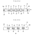
Figs. 3 are single piece view of the flexible print circuit board shown inFig. 1 , in whichFig. 3A is a front side view andFig. 3B is a back side view; -
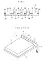
Fig. 4 is a view illustrating a state where the point-like light source is surface-mounted on the flexible print circuit board shown inFig. 3A ; and -
Fig. 5 is a perspective view illustrating a conventional planar illumination device. -
- 1
- Planar illumination device
- 2
- Light guide plate
- 3
- Point-like light source
- 5a
- Radiator plate
- 10
- Flexible print circuit board
- 10F
- Front side face
- 10R
- Back side face
- 12
- Land portion
- 14
- Conductor pattern
- 16
- Through hole
- 18
- High heat-conductive resin
- 20
- Conductor pattern
- 26
- Heat conductive resin having fluidity
- A
- Region
- Embodiments of the present invention will be described below based on the attached drawings. Here, the same portions or portions corresponding to the prior art are indicated by the same reference numerals and detailed description will be omitted.
-
Fig. 1 shows a flexible print circuit board (FPC) 10 on which a large-current type LED is surface-mounted as the point-likelight source 3 in a section of a planar illumination device according to the embodiment of the present invention. TheFPC 10 has the same basic configuration such as outline and thickness as theFPC 4 shown inFig. 5 . Specifically, as shown inFigs. 3A and 3B , aconductor pattern 14 continuing to aland portion 12 where anelectrode terminal 3a of the point-likelight source 3 is mounted on a front side face 10F is formed. Thisconductor pattern 14 is formed with the same constant width as a width W of theland portion 12. In order to effectively achieve self-alignment in the biaxial direction in a plane of the FPC when the point-likelight source 3 is mounted, the width of the conductor pattern needs to be made narrower than the width of the land portion, but because of a reason, which will be described later, the width of the conductor pattern may be formed with substantially the same constant width as the width W of theland portion 12. A portion indicated by thereference character 14a inFig. 3A is a land portion for connection to the outside. To theconductor pattern 14 continuing to theland portion 12, a throughhole 16 is formed. On a wall surface of the throughhole 16, aplating film 16a is formed. The sectional shape of the throughhole 16 is preferably circular, when considering workability, but the shape is not necessarily limited to that. For formation of the throughhole 16 and theplating film 16a, a process for producing a double-sided type FPC can be fully or partially used. - A region A of a
back side face 10R of theFPC 10 where at least the throughhole 16 is formed is bonded to aradiator plate 5a made of metal through a high heat-conductive resin 18 as shown inFig. 1 . The high heat-conductive resin 18 has electric insulation properties, and a silicon resin material or a high heat-conductive resin material in which a nonconductive heat conductive filler such as alumina, aluminum nitride, silicon carbide or the like is added can be used. - In the region A on the
back side face 10R of theFPC 10 where at least the throughhole 16 is formed, aconductive pattern 20 continuing to theplating film 16a applied on the throughhole 16 is formed. Both theconductive patterns flexible base film 22 made of polyimide or the like and moreover, covered by aflexible cover film 24 such as polyimide so as to cover theconductive patterns - In an example shown in
Fig. 1 , the high heat-conductive resin 18 is molded in the tape state. The tape-state high heat-conductive resin 18 is in a solid form when being applied between theback side face 10R of theFPC 10 and theradiator plate 5a, and it is excellent in workability. However, by using a high heat-conductive resin 26 having fluidity at least when being applied between theback side face 10R of theFPC 10 and theradiator plate 5a instead of the tape-state high heat-conductive resin 18, as shown inFig. 2 , the heat-conductive resin can be filled in the whole or a part within the throughhole 16. As the high heat-conductive resin 26 having fluidity, a resin material of a type having considerable fluidity and not requiring a drying / solidifying process such as silicon compound, adhesives, gel-state resins and the like can be cited. In this case, since the surface of the throughhole 16 is covered by thecover film 24, the high heat-conductive resin 26 does not protrude to thefront side face 10F of theFPC 10, and since the high heat-conductive resin 26 is held between thebase film 22 and thecover film 24 and brought into a sealed state, there is a merit that the high heat-conductive resin 18 does not have to be dried and solidified. -
Fig. 4 shows a state where the point-likelight source 3 is mounted on thefront side face 10F of theFPC 10 shown inFig. 3A . - Though detailed description will be omitted, the planar illumination device according to this embodiment of the present invention has the same basic configuration having a light guide plate, a point-like light source arranged on a side end face of the light guide plate, and a flexible print circuit board in which the point-like light source is mounted on the front side face as the conventional planar illumination device (See
Fig. 5 ). - According to the embodiment of the present invention configured as above, the following working effects can be obtained. First, a radiation path is constituted through which heat generated from the point-like
light source 3 is transmitted to theradiator plate 5a made of metal through theelectrode terminal 3a of the point-likelight source 3, theland portion 12 on thefront side face 10F of theFPC 10, the throughhole 16 of theconductive pattern 14, and the high heat-conductive resins conductor pattern 14 of theFPC 10 to theradiator plate 5a made of metal is extended, and a direct radiation area is also sufficiently ensured. Particularly, even if a large-current type LED is used for the point-likelight source 3, a sufficient radiation effect can be obtained. Also, since freedom of wiring pattern of theFPC 10 and freedom of outline are not different from a conventional FPC at all, demand for thinning of a planar illumination device can be sufficiently satisfied. - Also, since the
conductor pattern 20 continuing to theplating film 16a applied in the throughhole 16 is formed in the region A on theback side face 10R of theFPC 10 where at least the throughhole 16 is formed, a radiation path is constituted through which the heat generated from the point-likelight source 3 is transmitted to theradiator plate 5a made of metal through theelectrode terminal 3a of the point-like light source, theland portion 12 on thefront side face 10F of theFPC 10, theplating film 16a in the throughhole 16 of theconductor pattern 14, theconductor pattern 20 on theback side face 10R of theFPC 10, and the high heat-conductive resins conductor pattern 14 of theFPC 10 to theradiator plate 5a made of metal is extended, and the above working effect can be obtained efficiently. - The
conductor pattern 20 on theback side face 10R of theFPC 10 has a main purpose of improving the radiation performance, and it is sufficient if the pattern is provided only on the region A where the throughhole 16 is formed, but the pattern may be extended as necessary similarly to theconductor pattern 14 on thefront side face 10F. - If the high heat-
conductive resin 26 has fluidity at least when being applied between theback side face 10R of theFPC 10 and theradiator plate 5a and is filled within the throughhole 16, a radiation path is constituted through which the heat radiated from the point-likelight source 3 is transmitted to theradiator plate 5a made of metal through theelectrode terminal 3a of the point-likelight source 3, theland portion 12 on thefront side face 10F of theFPC 10, theplating film 16a and the high heat-conductive resin 26 in the throughhole 16 of theconductor pattern 14, and the high heat-conductive resin 26 as well as the high heat-conductive resin 26 applied between theback side face 10R of theFPC 10 and theradiator plate 5a. Therefore, the radiation path for efficient radiation from theconductor pattern 14 of theFPC 10 to theradiator plate 5a made of metal is further extended and the above working effect can be obtained further greatly. - Moreover, since the
conductor patterns FPC 10 where at least the throughhole 16 is formed are formed with the width larger than the width W of theland portion 12, a sectional area required for theconductor patterns holes 16 as possible for radiation can be installed. Specifically, since the width W of theconductor patterns light source 3 is easily transmitted to theconductor pattern 14 side through theland portion 12. Also, since the width W of theconductor patterns hole 16 can be ensured wide, and as many throughholes 16 as possible can be installed. - It is only necessary that the
conductor patterns land portion 12, and thus, the width may be expanded from a constant width substantially equal to the width W of theland portion 12 to a constant width larger than the width W of the land portion. Also, as long as the width larger than the width W of theland portion 12 is ensured, the width does not have to be constant but may be expanded / contracted as necessary, or the width other than the region A where the throughhole 16 is formed may be narrowed. - Moreover, from the following reason, the width W of the
land portion 12 of theFPC 10 is preferably equal to the width of theelectrode terminal 3a of the point-likelight source 3. That is, theland portion 12 has a structure that thecover film 24 is removed and the conductor is exposed, but since the width W of theland proton 12 is substantially equal to the width of theelectrode terminal 3a and also theconductor pattern 14 continuing to theland portion 12 has the width substantially equal to (or larger than) the width W of theland portion 12, mechanical strength of theconductor pattern 14 is drastically improved, and even if some impact force is applied to theFPC 10 during assembling of the planar illumination device or after assembling into the device, no disconnection occurs in theland portion 12. - Moreover, when the point-like
light source 3 is mounted on theFPC 10 by a reflow process, the point-likelight source 3 can be positioned to a predetermined position on theFPC 10 with high accuracy owing to the self-alignment effect. - When the
conductor pattern 14 continuing to theland portion 12 has the width substantially equal to (or larger than) the width W of theland portion 12, it is worried that the self-alignment effect is weakened in the extension direction of the conductor pattern 14 (direction from theland portion 12 to aland portion 14a for outside connection in the example inFig. 3 ). However, even if the position of the point-likelight source 3 is displaced in the extension direction of theconductor pattern 14, a plurality of same-shaped prisms extending in the thickness direction of the light guide plate are arranged on an incoming-light face 2a (Fig. 5 ) of thelight guide plate 2 in the extension direction of theconductor pattern 14 so as to constitute diffusing means, the incidence rate of light from the point-likelight source 3 to thelight guide plate 2 is scarcely changed. Therefore, even if the self-alignment effect in the extension direction of theconductor pattern 14 is weakened, characteristics as the planar illumination device are not affected. - It should be understood that the point-like
light source 3 mounted on theFPC 10 can be applied not only to a case where its outgoing face is the face on the side opposite the one where theelectrode terminal 3a of the point-likelight source 3 is provided as shown in the example inFig. 5 (that is, theFPC 4 inFig. 5 is totally replaced by theFPC 10 according to the embodiment of the present invention) but also to a case where a face crossing the face on which theelectrode terminal 3a of the point-likelight source 3 is provided is an outgoing face. - Also, in the embodiment of the present invention, a case where the radiation path from the point-like
light source 3 to theradiator plate 5a made of metal is formed on theFPC 10 is described as an example, but it should be understood that the radiation path can be similarly applied to a case where another print circuit board other than FPC is used.
Claims (4)
- A planar illumination device comprising a light guide plate, a point-like light source arranged on the side end face of the light guide plate, and a print circuit board, the front side face of which is provided with the point-like light source,
characterized in that:a through hole is formed on a conductor pattern continuing to a land portion in the print circuit board where the point-like light source is mounted; anda region on the back side face of the print circuit board where at least the through hole is formed is bonded to a radiator plate through a high heat-conductive resin. - The planar illumination device according to claim 1, wherein on the region of the back side face of the print circuit board where at least the through hole is formed, a conductor pattern continuing to a plating film applied on the through hole is fabricated.
- The planar illumination device according to claim 1 or 2, wherein the high heat-conductive resin is filled in the through hole while retaining fluidity in application at least between the back side face of the print circuit board and the radiator plate.
- The planar illumination device according to any one of claims 1 to 3, wherein a conductor pattern in a region where at least the through hole is formed in the print circuit board is fabricated with a width larger than the width of the land portion.
Applications Claiming Priority (2)
| Application Number | Priority Date | Filing Date | Title |
|---|---|---|---|
| JP2005168429A JP4697533B2 (en) | 2005-06-08 | 2005-06-08 | Surface lighting device |
| PCT/JP2006/311421 WO2006132271A1 (en) | 2005-06-08 | 2006-06-07 | Surface illuminator |
Publications (1)
| Publication Number | Publication Date |
|---|---|
| EP1895229A1 true EP1895229A1 (en) | 2008-03-05 |
Family
ID=37498470
Family Applications (1)
| Application Number | Title | Priority Date | Filing Date |
|---|---|---|---|
| EP06757128A Withdrawn EP1895229A1 (en) | 2005-06-08 | 2006-06-07 | Surface illuminator |
Country Status (4)
| Country | Link |
|---|---|
| US (1) | US20090207630A1 (en) |
| EP (1) | EP1895229A1 (en) |
| JP (1) | JP4697533B2 (en) |
| WO (1) | WO2006132271A1 (en) |
Families Citing this family (31)
| Publication number | Priority date | Publication date | Assignee | Title |
|---|---|---|---|---|
| GB2448270B (en) * | 2006-02-10 | 2012-02-08 | Innovatech Ltd | Circuit board and radiating heat system for circuit board |
| JP2008166304A (en) * | 2006-12-26 | 2008-07-17 | Sony Corp | Backlight device and liquid crystal display device |
| JP4939970B2 (en) * | 2007-02-20 | 2012-05-30 | ニューパラダイムテクノロジー株式会社 | Planar light emitting structure |
| TW200846250A (en) * | 2007-05-18 | 2008-12-01 | Pyroswift Folding Co Ltd | Manufacture method of tag-typed integrated soft circuit board and a structure thereof |
| EP2149281B1 (en) * | 2007-05-22 | 2012-06-27 | Osram AG | Illumination device and projection device with such an illumination device |
| DE102007055133A1 (en) * | 2007-11-19 | 2009-05-20 | Osram Gesellschaft mit beschränkter Haftung | Lighting device with a heat sink |
| JP4740964B2 (en) * | 2008-01-11 | 2011-08-03 | 国分電機株式会社 | LED downlight |
| KR20090131175A (en) * | 2008-06-17 | 2009-12-28 | 삼성전자주식회사 | Backlight unit for liquid crystal display device |
| WO2010130212A1 (en) * | 2009-05-14 | 2010-11-18 | 浙江西子光电科技有限公司 | Led illuminator and led module |
| JP5286206B2 (en) | 2009-09-11 | 2013-09-11 | 日立コンシューマエレクトロニクス株式会社 | Liquid crystal display |
| KR20140020446A (en) * | 2012-08-08 | 2014-02-19 | 삼성디스플레이 주식회사 | Back light assembly and display apparatus having the same |
| JP5991891B2 (en) * | 2012-09-12 | 2016-09-14 | ミネベア株式会社 | Surface lighting device |
| US8998454B2 (en) * | 2013-03-15 | 2015-04-07 | Sumitomo Electric Printed Circuits, Inc. | Flexible electronic assembly and method of manufacturing the same |
| CN103336388A (en) * | 2013-07-16 | 2013-10-02 | 深圳市华星光电技术有限公司 | Backlight unit |
| CN103687314B (en) * | 2013-12-07 | 2016-08-17 | 广东达进电子科技有限公司 | A kind of manufacture method of novel aluminum base circuit board |
| KR102411999B1 (en) * | 2015-04-08 | 2022-06-22 | 삼성전기주식회사 | Circuit board |
| JP6614792B2 (en) * | 2015-04-28 | 2019-12-04 | 三菱電機株式会社 | Light source unit and lighting device |
| US9706639B2 (en) * | 2015-06-18 | 2017-07-11 | Samsung Electro-Mechanics Co., Ltd. | Circuit board and method of manufacturing the same |
| JP6780955B2 (en) * | 2016-05-02 | 2020-11-04 | 株式会社小糸製作所 | Light source unit and lamp |
| CN106280856A (en) * | 2016-05-23 | 2017-01-04 | 庄可香 | A negative ion LED energy-saving environmental protection lamp |
| JP6408516B2 (en) * | 2016-07-01 | 2018-10-17 | ミネベアミツミ株式会社 | Surface illumination device and substrate |
| CN107783222B (en) * | 2016-08-26 | 2020-07-14 | 美蓓亚三美株式会社 | Planar lighting device and substrate |
| JP6619373B2 (en) * | 2016-12-13 | 2019-12-11 | ミネベアミツミ株式会社 | Planar illumination device and method of manufacturing planar illumination device |
| DE102018111554A1 (en) * | 2018-05-15 | 2019-11-21 | HELLA GmbH & Co. KGaA | Printed circuit board structure for receiving at least one semiconductor illuminant |
| JP7094182B2 (en) * | 2018-08-29 | 2022-07-01 | 株式会社小糸製作所 | Lamp unit |
| JP6796746B1 (en) * | 2019-02-21 | 2020-12-09 | ミネベアミツミ株式会社 | Planar lighting device |
| US11626448B2 (en) | 2019-03-29 | 2023-04-11 | Lumileds Llc | Fan-out light-emitting diode (LED) device substrate with embedded backplane, lighting system and method of manufacture |
| US11156346B2 (en) | 2019-11-19 | 2021-10-26 | Lumileds Llc | Fan out structure for light-emitting diode (LED) device and lighting system |
| US11777066B2 (en) | 2019-12-27 | 2023-10-03 | Lumileds Llc | Flipchip interconnected light-emitting diode package assembly |
| US11664347B2 (en) | 2020-01-07 | 2023-05-30 | Lumileds Llc | Ceramic carrier and build up carrier for light-emitting diode (LED) array |
| US11476217B2 (en) | 2020-03-10 | 2022-10-18 | Lumileds Llc | Method of manufacturing an augmented LED array assembly |
Family Cites Families (12)
| Publication number | Priority date | Publication date | Assignee | Title |
|---|---|---|---|---|
| DE3813364A1 (en) * | 1988-04-21 | 1989-11-02 | Bodenseewerk Geraetetech | DEVICE FOR HEAT EXHAUSTING COMPONENTS ON A CIRCUIT BOARD |
| US5857767A (en) * | 1996-09-23 | 1999-01-12 | Relume Corporation | Thermal management system for L.E.D. arrays |
| JP4056598B2 (en) * | 1997-10-09 | 2008-03-05 | シチズン電子株式会社 | Infrared data communication module |
| DE19842590A1 (en) * | 1998-09-17 | 2000-04-13 | Daimler Chrysler Ag | Process for the production of circuit arrangements |
| KR100419611B1 (en) * | 2001-05-24 | 2004-02-25 | 삼성전기주식회사 | A Light Emitting Diode, a Lighting Emitting Device Using the Same and a Fabrication Process therefor |
| JP2003076287A (en) * | 2001-09-04 | 2003-03-14 | Sony Corp | Backlight device |
| KR20090115810A (en) * | 2001-12-29 | 2009-11-06 | 항조우 후양 신잉 띠앤즈 리미티드 | LED and LED lamps |
| JP2003324214A (en) * | 2002-04-30 | 2003-11-14 | Omron Corp | Light emitting module |
| JP4211029B2 (en) * | 2003-07-17 | 2009-01-21 | 三菱電機株式会社 | Surface light source device |
| US6966674B2 (en) * | 2004-02-17 | 2005-11-22 | Au Optronics Corp. | Backlight module and heat dissipation structure thereof |
| JP2005340684A (en) * | 2004-05-31 | 2005-12-08 | Calsonic Kansei Corp | Attaching structure of electronic element to substrate |
| US7168842B2 (en) * | 2004-12-01 | 2007-01-30 | Au Optronics Corporation | Light emitting diode backlight package |
-
2005
- 2005-06-08 JP JP2005168429A patent/JP4697533B2/en not_active Expired - Fee Related
-
2006
- 2006-06-07 EP EP06757128A patent/EP1895229A1/en not_active Withdrawn
- 2006-06-07 WO PCT/JP2006/311421 patent/WO2006132271A1/en not_active Ceased
- 2006-06-07 US US11/921,787 patent/US20090207630A1/en not_active Abandoned
Non-Patent Citations (1)
| Title |
|---|
| See references of WO2006132271A1 * |
Also Published As
| Publication number | Publication date |
|---|---|
| US20090207630A1 (en) | 2009-08-20 |
| WO2006132271A1 (en) | 2006-12-14 |
| JP4697533B2 (en) | 2011-06-08 |
| JP2006344472A (en) | 2006-12-21 |
Similar Documents
| Publication | Publication Date | Title |
|---|---|---|
| US20090207630A1 (en) | Planar illumination device | |
| JP4654942B2 (en) | Surface lighting device | |
| KR100764380B1 (en) | Slim backlight unit | |
| US20090201699A1 (en) | Planar Illumination Device and Manufacturing Method of Same | |
| US8071998B2 (en) | Light emitting assembly | |
| US20100301376A1 (en) | Side view type led package | |
| JP4969332B2 (en) | Substrate and lighting device | |
| EP1544915A3 (en) | Electronic module heat sink mounting arrangement | |
| CN210123135U (en) | LED light equipment for vehicles | |
| CN103925519B (en) | Circuit board and the flat-panel monitor including the circuit board | |
| KR101545941B1 (en) | Light source, light output module having the same, and backlight assembly | |
| JP2010238540A (en) | Light emitting module and manufacturing method thereof | |
| KR101629663B1 (en) | Daytime Running Light Module | |
| JP4721161B2 (en) | Surface lighting device | |
| KR101221568B1 (en) | Backlight Unit having LEDs and Method for manufacturing the same | |
| JP2006210183A (en) | Surface lighting device | |
| KR100791594B1 (en) | Lighting device with a heat radiating part | |
| CN116896815A (en) | Circuit board of optical machine module, optical machine module and AR equipment | |
| CN113483282A (en) | Flexible lamp strip with flip LED chip and manufacturing method thereof | |
| CN219834478U (en) | Micro LED electric connection structure | |
| CN218998358U (en) | Multilayer printed circuit board | |
| US20070018311A1 (en) | Circuit board and light souce device having same | |
| CN214223034U (en) | Lighting device and vehicle | |
| KR100604619B1 (en) | Electronic controller | |
| KR20090113115A (en) | Leadframe with Effective Heat Dissipation Structure for High Power Light Source Lamp, Electronic Device and Manufacturing Method Thereof |
Legal Events
| Date | Code | Title | Description |
|---|---|---|---|
| PUAI | Public reference made under article 153(3) epc to a published international application that has entered the european phase |
Free format text: ORIGINAL CODE: 0009012 |
|
| 17P | Request for examination filed |
Effective date: 20071231 |
|
| AK | Designated contracting states |
Kind code of ref document: A1 Designated state(s): DE |
|
| DAX | Request for extension of the european patent (deleted) | ||
| RBV | Designated contracting states (corrected) |
Designated state(s): DE |
|
| DAX | Request for extension of the european patent (deleted) | ||
| STAA | Information on the status of an ep patent application or granted ep patent |
Free format text: STATUS: THE APPLICATION IS DEEMED TO BE WITHDRAWN |
|
| 18D | Application deemed to be withdrawn |
Effective date: 20110104 |