EP1892807A1 - DBR for a VCSEL having layers with unequal optical thickness - Google Patents
DBR for a VCSEL having layers with unequal optical thickness Download PDFInfo
- Publication number
- EP1892807A1 EP1892807A1 EP07015270A EP07015270A EP1892807A1 EP 1892807 A1 EP1892807 A1 EP 1892807A1 EP 07015270 A EP07015270 A EP 07015270A EP 07015270 A EP07015270 A EP 07015270A EP 1892807 A1 EP1892807 A1 EP 1892807A1
- Authority
- EP
- European Patent Office
- Prior art keywords
- layer
- optical
- optical device
- optical thickness
- reflector
- Prior art date
- Legal status (The legal status is an assumption and is not a legal conclusion. Google has not performed a legal analysis and makes no representation as to the accuracy of the status listed.)
- Granted
Links
Images


Classifications
-
- H—ELECTRICITY
- H01—ELECTRIC ELEMENTS
- H01S—DEVICES USING THE PROCESS OF LIGHT AMPLIFICATION BY STIMULATED EMISSION OF RADIATION [LASER] TO AMPLIFY OR GENERATE LIGHT; DEVICES USING STIMULATED EMISSION OF ELECTROMAGNETIC RADIATION IN WAVE RANGES OTHER THAN OPTICAL
- H01S5/00—Semiconductor lasers
- H01S5/10—Construction or shape of the optical resonator, e.g. extended or external cavity, coupled cavities, bent-guide, varying width, thickness or composition of the active region
- H01S5/18—Surface-emitting [SE] lasers, e.g. having both horizontal and vertical cavities
- H01S5/183—Surface-emitting [SE] lasers, e.g. having both horizontal and vertical cavities having only vertical cavities, e.g. vertical cavity surface-emitting lasers [VCSEL]
- H01S5/18361—Structure of the reflectors, e.g. hybrid mirrors
- H01S5/18369—Structure of the reflectors, e.g. hybrid mirrors based on dielectric materials
-
- B—PERFORMING OPERATIONS; TRANSPORTING
- B82—NANOTECHNOLOGY
- B82Y—SPECIFIC USES OR APPLICATIONS OF NANOSTRUCTURES; MEASUREMENT OR ANALYSIS OF NANOSTRUCTURES; MANUFACTURE OR TREATMENT OF NANOSTRUCTURES
- B82Y20/00—Nanooptics, e.g. quantum optics or photonic crystals
-
- H—ELECTRICITY
- H01—ELECTRIC ELEMENTS
- H01S—DEVICES USING THE PROCESS OF LIGHT AMPLIFICATION BY STIMULATED EMISSION OF RADIATION [LASER] TO AMPLIFY OR GENERATE LIGHT; DEVICES USING STIMULATED EMISSION OF ELECTROMAGNETIC RADIATION IN WAVE RANGES OTHER THAN OPTICAL
- H01S5/00—Semiconductor lasers
- H01S5/10—Construction or shape of the optical resonator, e.g. extended or external cavity, coupled cavities, bent-guide, varying width, thickness or composition of the active region
- H01S5/18—Surface-emitting [SE] lasers, e.g. having both horizontal and vertical cavities
- H01S5/183—Surface-emitting [SE] lasers, e.g. having both horizontal and vertical cavities having only vertical cavities, e.g. vertical cavity surface-emitting lasers [VCSEL]
- H01S5/18361—Structure of the reflectors, e.g. hybrid mirrors
-
- H—ELECTRICITY
- H01—ELECTRIC ELEMENTS
- H01L—SEMICONDUCTOR DEVICES NOT COVERED BY CLASS H10
- H01L33/00—Semiconductor devices with at least one potential-jump barrier or surface barrier specially adapted for light emission; Processes or apparatus specially adapted for the manufacture or treatment thereof or of parts thereof; Details thereof
- H01L33/02—Semiconductor devices with at least one potential-jump barrier or surface barrier specially adapted for light emission; Processes or apparatus specially adapted for the manufacture or treatment thereof or of parts thereof; Details thereof characterised by the semiconductor bodies
- H01L33/10—Semiconductor devices with at least one potential-jump barrier or surface barrier specially adapted for light emission; Processes or apparatus specially adapted for the manufacture or treatment thereof or of parts thereof; Details thereof characterised by the semiconductor bodies with a light reflecting structure, e.g. semiconductor Bragg reflector
- H01L33/105—Semiconductor devices with at least one potential-jump barrier or surface barrier specially adapted for light emission; Processes or apparatus specially adapted for the manufacture or treatment thereof or of parts thereof; Details thereof characterised by the semiconductor bodies with a light reflecting structure, e.g. semiconductor Bragg reflector with a resonant cavity structure
-
- H—ELECTRICITY
- H01—ELECTRIC ELEMENTS
- H01S—DEVICES USING THE PROCESS OF LIGHT AMPLIFICATION BY STIMULATED EMISSION OF RADIATION [LASER] TO AMPLIFY OR GENERATE LIGHT; DEVICES USING STIMULATED EMISSION OF ELECTROMAGNETIC RADIATION IN WAVE RANGES OTHER THAN OPTICAL
- H01S5/00—Semiconductor lasers
- H01S5/10—Construction or shape of the optical resonator, e.g. extended or external cavity, coupled cavities, bent-guide, varying width, thickness or composition of the active region
- H01S5/18—Surface-emitting [SE] lasers, e.g. having both horizontal and vertical cavities
- H01S5/183—Surface-emitting [SE] lasers, e.g. having both horizontal and vertical cavities having only vertical cavities, e.g. vertical cavity surface-emitting lasers [VCSEL]
- H01S5/18358—Surface-emitting [SE] lasers, e.g. having both horizontal and vertical cavities having only vertical cavities, e.g. vertical cavity surface-emitting lasers [VCSEL] containing spacer layers to adjust the phase of the light wave in the cavity
-
- H—ELECTRICITY
- H01—ELECTRIC ELEMENTS
- H01S—DEVICES USING THE PROCESS OF LIGHT AMPLIFICATION BY STIMULATED EMISSION OF RADIATION [LASER] TO AMPLIFY OR GENERATE LIGHT; DEVICES USING STIMULATED EMISSION OF ELECTROMAGNETIC RADIATION IN WAVE RANGES OTHER THAN OPTICAL
- H01S5/00—Semiconductor lasers
- H01S5/30—Structure or shape of the active region; Materials used for the active region
- H01S5/32—Structure or shape of the active region; Materials used for the active region comprising PN junctions, e.g. hetero- or double- heterostructures
- H01S5/3201—Structure or shape of the active region; Materials used for the active region comprising PN junctions, e.g. hetero- or double- heterostructures incorporating bulkstrain effects, e.g. strain compensation, strain related to polarisation
-
- H—ELECTRICITY
- H01—ELECTRIC ELEMENTS
- H01S—DEVICES USING THE PROCESS OF LIGHT AMPLIFICATION BY STIMULATED EMISSION OF RADIATION [LASER] TO AMPLIFY OR GENERATE LIGHT; DEVICES USING STIMULATED EMISSION OF ELECTROMAGNETIC RADIATION IN WAVE RANGES OTHER THAN OPTICAL
- H01S5/00—Semiconductor lasers
- H01S5/30—Structure or shape of the active region; Materials used for the active region
- H01S5/34—Structure or shape of the active region; Materials used for the active region comprising quantum well or superlattice structures, e.g. single quantum well [SQW] lasers, multiple quantum well [MQW] lasers or graded index separate confinement heterostructure [GRINSCH] lasers
- H01S5/343—Structure or shape of the active region; Materials used for the active region comprising quantum well or superlattice structures, e.g. single quantum well [SQW] lasers, multiple quantum well [MQW] lasers or graded index separate confinement heterostructure [GRINSCH] lasers in AIIIBV compounds, e.g. AlGaAs-laser, InP-based laser
- H01S5/34306—Structure or shape of the active region; Materials used for the active region comprising quantum well or superlattice structures, e.g. single quantum well [SQW] lasers, multiple quantum well [MQW] lasers or graded index separate confinement heterostructure [GRINSCH] lasers in AIIIBV compounds, e.g. AlGaAs-laser, InP-based laser emitting light at a wavelength longer than 1000nm, e.g. InP based 1300 and 1500nm lasers
-
- H—ELECTRICITY
- H01—ELECTRIC ELEMENTS
- H01S—DEVICES USING THE PROCESS OF LIGHT AMPLIFICATION BY STIMULATED EMISSION OF RADIATION [LASER] TO AMPLIFY OR GENERATE LIGHT; DEVICES USING STIMULATED EMISSION OF ELECTROMAGNETIC RADIATION IN WAVE RANGES OTHER THAN OPTICAL
- H01S5/00—Semiconductor lasers
- H01S5/30—Structure or shape of the active region; Materials used for the active region
- H01S5/34—Structure or shape of the active region; Materials used for the active region comprising quantum well or superlattice structures, e.g. single quantum well [SQW] lasers, multiple quantum well [MQW] lasers or graded index separate confinement heterostructure [GRINSCH] lasers
- H01S5/343—Structure or shape of the active region; Materials used for the active region comprising quantum well or superlattice structures, e.g. single quantum well [SQW] lasers, multiple quantum well [MQW] lasers or graded index separate confinement heterostructure [GRINSCH] lasers in AIIIBV compounds, e.g. AlGaAs-laser, InP-based laser
- H01S5/34333—Structure or shape of the active region; Materials used for the active region comprising quantum well or superlattice structures, e.g. single quantum well [SQW] lasers, multiple quantum well [MQW] lasers or graded index separate confinement heterostructure [GRINSCH] lasers in AIIIBV compounds, e.g. AlGaAs-laser, InP-based laser with a well layer based on Ga(In)N or Ga(In)P, e.g. blue laser
-
- H—ELECTRICITY
- H01—ELECTRIC ELEMENTS
- H01S—DEVICES USING THE PROCESS OF LIGHT AMPLIFICATION BY STIMULATED EMISSION OF RADIATION [LASER] TO AMPLIFY OR GENERATE LIGHT; DEVICES USING STIMULATED EMISSION OF ELECTROMAGNETIC RADIATION IN WAVE RANGES OTHER THAN OPTICAL
- H01S5/00—Semiconductor lasers
- H01S5/30—Structure or shape of the active region; Materials used for the active region
- H01S5/34—Structure or shape of the active region; Materials used for the active region comprising quantum well or superlattice structures, e.g. single quantum well [SQW] lasers, multiple quantum well [MQW] lasers or graded index separate confinement heterostructure [GRINSCH] lasers
- H01S5/343—Structure or shape of the active region; Materials used for the active region comprising quantum well or superlattice structures, e.g. single quantum well [SQW] lasers, multiple quantum well [MQW] lasers or graded index separate confinement heterostructure [GRINSCH] lasers in AIIIBV compounds, e.g. AlGaAs-laser, InP-based laser
- H01S5/34346—Structure or shape of the active region; Materials used for the active region comprising quantum well or superlattice structures, e.g. single quantum well [SQW] lasers, multiple quantum well [MQW] lasers or graded index separate confinement heterostructure [GRINSCH] lasers in AIIIBV compounds, e.g. AlGaAs-laser, InP-based laser characterised by the materials of the barrier layers
- H01S5/3436—Structure or shape of the active region; Materials used for the active region comprising quantum well or superlattice structures, e.g. single quantum well [SQW] lasers, multiple quantum well [MQW] lasers or graded index separate confinement heterostructure [GRINSCH] lasers in AIIIBV compounds, e.g. AlGaAs-laser, InP-based laser characterised by the materials of the barrier layers based on InGa(Al)P
Abstract
Description
- The present invention relates to an optical device including a multilayer reflector.
- (vertical Cavity Surface Emitting Laser)
- A vertical cavity surface emitting laser (VCSEL) which is an optical device can emit light in a direction perpendicular to a semiconductor substrate, so a two-dimensional array can be easily formed. When parallel processing of multibeam emitted from the two-dimensional array is performed, higher density and higher speed can be obtained, so various industrial applications are expected. For example, when a vertical cavity surface emitting laser array is used as an exposure source of an electrophotographic printer, the printing speed can be increased by parallel processing of a printing process using the multibeam.
- A vertical cavity surface emitting laser which is currently in practical use is a device for mainly generating laser light of an infrared region (0.75 µm to 0.85 µm). A beam spot can be further reduced as an oscillation wavelength is shortened from the infrared region to a red region, a blue region, and an ultraviolet region, so higher resolution can be obtained. Therefore, the practical use of a vertical cavity surface emitting laser in the regions from red to ultraviolet is required.
- There is a great effect attained by a combination of the increase in resolution which is obtained by the shortened wavelength and the parallel processing using the multibeam, its contribution to various fields including applications for a printer is expected. When a vertical cavity surface emitting laser capable of oscillating in a band of from 1.3 µm to 1.5 µm in which dispersion or absorption in an optical fiber is small can be in practical use, long-distance large-capacity communications can be performed using an arrayed fiber and an arrayed optical source.
- (Multilayer Reflector)
- The feature of the vertical cavity surface emitting laser is to include a cavity provided in a direction perpendicular to an in-plane direction of a substrate. In order to realize a surface-emitting laser which can continuously operate at a room temperature, a reflector whose reflectivity is 99% or more is necessary.
- An example of such a reflector to be used includes a multilayer reflector in which two materials whose refractive indices are different from each other are alternately laminated plural times by an optical thickness of λ/4. Here, λ denotes a wavelength of light emitted from an optical device. The optical thickness is obtained by multiplying a thickness of a layer by a refractive index of a material of the layer.
- (Near-Infrared Vertical Cavity Surface Emitting Laser)
- For a near-infrared vertical cavity surface emitting laser using a GaAs semiconductor which is already in a practical use, a semiconductor multilayer mirror in which GaAs and AlAs which have extremely high crystallinity are combined is used. In addition, a semiconductor multilayer mirror in which AlGaAs whose Al composition is small and AlGaAs whose Al composition is large are combined for constituent layers is used.
- However, a long-wavelength (1.3 µm to 1.5 µm) laser for communication and a red (0.62 µm to 0.7 µm) laser have a problem in that their thermal characteristics are undesirable or high-power output is difficult to be achieved.
- That is, in an active layer for generating light of the communication wavelength region or the red region, there is no clad layer material capable of sufficiently confining electrons in the active layer at a high temperature ranging from 60°C to 80°C. Therefore, with an increase in temperature, a large number of electrons are overflowing from the active layer, so the thermal characteristics deteriorate and the high-power output is difficult to perform.
- In the vertical cavity surface emitting laser, heat generated by the active layer is confined to the vicinities of the active layer by the semiconductor multilayer reflector whose thermal resistance is high.
- Therefore, unfortunately, the vertical cavity surface emitting lasers using the material for generating the light of the above-mentioned wavelength are devices whose temperature characteristics are undesirable.
- To be specific, a normal multilayer reflector of the long-wavelength vertical cavity surface emitting laser has a structure in which an InGaAsP layer (high refractive index layer) whose optical thickness is λ/4 and an InP layer (low refractive index layer) whose optical thickness is λ/4 are alternately laminated as a large number of pairs. In this case, the thermal resistance of the InGaAsP layer used as the high refractive index layer is approximately 20 times larger than the thermal resistance of the InP layer used as the low refractive index layer.
- In the circumstances, in 47th Seiken Symposium Preprints, pp.80-81, March 2006 (Precision and Intelligence Laboratory, Tokyo Institute of Technology), a multilayer reflector in which the optical thickness of a multilayer reflector constituent layer is not set to λ/4 is discussed.
- To be specific, with respect to the multilayer reflector of the long-wavelength vertical cavity surface emitting laser, in 47th Seiken Symposium Preprints, pp.80-81, March 2006 (Precision and Intelligence Laboratory, Tokyo Institute of Technology), a multilayer reflector in which the optical thickness of an InP layer whose thermal resistance is small is set to a value larger than λ/4 and the optical thickness of an InGaAsP layer whose thermal resistance is large is set to a value smaller than λ/4 is disclosed in order to reduce the thermal resistance.
- The total layer thickness (one pair) of the high refractive index layer and the low refractive index layer which constitute the multilayer reflector is fixed to be an optical thickness of λ/2. Therefore, it is considered that a heat dissipation effect can be improved and thus it is possible to provide the multilayer reflector in which an increase in device temperature can be prevented.
- (Ultraviolet/Blue Vertical Cavity Surface Emitting Laser)
- A GaN semiconductor material is used for a vertical cavity surface emitting laser in an ultraviolet/blue region (300 µm to 500 µm). For a multilayer reflector, for example, a pair of a GaN material and an AlN material with a relatively large refractive index difference therebetween is selected.
- However, the multilayer reflector made of both of these materials has a large lattice mismatch. When several ten pairs are grown by an optical thickness of λ/4, it is more likely to introduce lattice strains into the multilayer by the lattice mismatch. As a result, a crack occurs, so it is difficult to form such a multilayer reflector as to achieve a reflectance of 99% or more.
- Therefore, also in
Japanese Patent Application Laid-Open No. 2003-107241 - To be specific, a multilayer reflector is disclosed in which the optical thickness of a GaN layer whose thermal expansion coefficient difference with respect to a substrate is small is set to a value larger than λ/4 and the optical thickness of a Al0.6Ga0.4N layer whose thermal expansion coefficient difference with respect to the substrate is large is set to a value smaller than λ/4.
- The total optical thickness (of one pair) of the high refractive index layer and the low refractive index layer which constitute the multilayer reflector is fixed to be an optical thickness of λ/2. Therefore, it is considered that the multilayer reflector with few cracks can be provided.
- In 47th Seiken Symposium Preprints, pp.80-81, March 2006 (Precision and Intelligence Laboratory, Tokyo Institute of Technology) and
Japanese Patent Application Laid-Open No. 2003-107241 - The inventor of the present invention arranged the layers whose optical thickness is not λ/4 as described in 47th Seiken Symposium Preprints, pp.80-81, March 2006 (Precision and Intelligence Laboratory, Tokyo Institute of Technology) and studied in view of a cavity structure. As a result, it was found that the arrangement causes a deviation of a design value from a resonance wavelength and a reduction in reflectivity.
- That is, when the arrangement of the high refractive index layer and the low refractive index layer with respect to the internal optical intensity distribution is not taken into account, it is likely to cause a reduction in yield due to the deviation of the resonance frequency or deterioration of device characteristics due to a reduction in reflectivity. As a result, although the intended use of the layer whose optical thickness is not λ/4 is made for improving the characteristics, a problem that the effect of such use cannot be obtained occurs.
- The present invention has been made to solve the above-mentioned problem and an object of the present invention is to provide an optical device including a reflector having a layer whose optical thickness is not λ/4, for which the resonance wavelength is made closer to a design value and a reduction in reflectivity is suppressed.
- According to the present invention, there is provided an optical device for generating light of a wavelength λ, including a reflector and an active layer, the reflector being a semiconductor multilayer reflector including a first layer and a second layer which are alternatively laminated and have refractive indices different from each other, wherein the first layer has an optical thickness smaller than λ/4 and the second layer has an optical thickness larger than λ/4, and an interface between the first layer and the second layer is located at a position other than a node and an antinode of an optical intensity distribution within the reflector.
- According to the present invention, with respect to the optical device including the reflector having the layer whose optical thickness is not λ/4, the resonance wavelength can be made closer to the design value and the reduction in reflectivity can be suppressed.
- Further features of the present invention will become apparent from the following description of exemplary embodiments with reference to the attached drawings.
- FIG. 1 is a schematic cross sectional view illustrating a structure of a vertical cavity surface emitting laser according to an embodiment of the present invention.
- FIGS. 2A, 2B, 2C, and 2D are enlarged schematic views illustrating resonator structures of the vertical cavity surface emitting laser of FIG. 1.
- FIG. 3 is a schematic cross sectional view illustrating a structure of a vertical cavity surface emitting laser according to Example 1.
- FIGS. 4A, 4B, 4C and 4D are enlarged schematic views illustrating resonator structures each including an AlAs/Al0.5Ga0.5As multilayer reflector and a Ga0.5In0.5P quantum well active layer as illustrated in FIGS. 2A to 2D.
- FIG. 5 illustrates a comparison between center wavelengths and reflectances in cases where only the multilayer reflector as illustrated in FIGS. 6A to 6D is taken into account.
- FIGS. 6A, 6B, 6C and 6D are enlarged schematic views illustrating structures in which only the AlAs/Al0.5Ga0.5As multilayer reflector is taken into account.
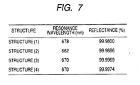
- FIG. 7 illustrates a comparison between center wavelengths and reflectances in cases where a resonator including the multilayer reflector and the active layer illustrated in FIGS. 4A to 4D is taken into account.
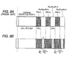
- FIGS. 8A and 8B are schematic explanatory views illustrating a specific structure (FIG. 8B) of Example 1 in comparison with a conventional example (FIG. 8A).
- FIG. 9 is a schematic cross sectional view illustrating a structure of a vertical cavity surface emitting laser according to Example 2.
- FIGS. 10A, 10B, 10C and 10D are enlarged schematic views illustrating resonator structures each including an AlN/GaN multilayer reflector and an InGaN quantum well active layer as illustrated in FIG. 9.
- FIG. 11 illustrates a comparison between center wavelengths and reflectances in cases where only the multilayer reflector as illustrated in FIGS. 12A to 12D is taken into account.
- FIGS. 12A, 12B, 12C and 12D are enlarged schematic views illustrating structures in which only the AlN/GaN multilayer reflector is taken into account.
- FIG. 13 illustrates a comparison between center wavelengths and reflectances in cases a resonator including the multilayer reflector and the active layer illustrated in FIGS. 10A to 10D are taken into account.
- FIGS. 14A and 14B are schematic explanatory views illustrating a specific structure (FIG. 14B) of Example 2 in comparison with a conventional example (FIG. 14A).
- FIG. 15 is a schematic cross sectional view illustrating a structure of a vertical cavity surface emitting laser according to Example 3.
- FIG. 16 is an enlarged schematic view illustrating a resonator structure including an AlN/GaN multilayer reflector and an InGaN quantum well active layer as illustrated in FIG. 15.
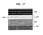
- FIG. 17 is a schematic cross sectional view illustrating a structure of a vertical cavity surface emitting laser according to Example 4.
- FIG. 18 is an enlarged schematic view illustrating a resonator structure including an AlN/GaN multilayer reflector and an InGaN quantum well active layer as illustrated in FIG. 17.
- FIG. 19 is a schematic explanatory view illustrating an electrophotographic apparatus using an optical device according to the present invention.
- Embodiments of the present invention will be described with reference to FIG. 1 and FIGS. 2A to 2D.
- FIG. 1 is a schematic cross sectional view illustrating a structure of an optical device according to an embodiment of the present invention. Here, an example of a vertical cavity surface emitting laser will be described. A
multilayer reflector 102, aspacer layer 103, anactive layer 104, aspacer layer 105, and amultilayer reflector 106 are provided on asubstrate 101. - FIGS. 2A to 2D are enlarged schematic views illustrating the
multilayer reflector 102, thespacer layer 103, and theactive layer 104 shown in FIG. 1. In the case of themultilayer reflector 102, only three pairs located close to theactive layer 104 are illustrated for the sake of convenience. FIGS. 2A and 2B illustrate reference examples, FIG. 2C illustrates an embodiment of the present invention, and FIG. 2D illustrates a conventional example. - A. Structure of Conventional Example
- In the conventional example shown in FIG. 2D, a multilayer reflector in which the optical thicknesses of both layers are λ/4 is constructed with conventional design values. As illustrated in FIG. 2D, the
multilayer reflector 102 includes alayer 110 and alayer 120 which are alternately laminated. Thelayer 120 has a refractive index different from the refractive index of thelayer 110. It is only required that thelayers layer 110 may be higher than or lower than the refractive index of thelayer 120. FIG. 2D illustrates the case where the refractive index of thelayer 120 is lower than the refractive index of thelayer 110. - B. Structures of Reference Examples
- In the reference examples of FIGS. 2A and 2B, a multilayer reflector in which the optical thicknesses of both layers deviate from λ/4 is constructed. As illustrated in FIGS. 2A and 2B, the multilayer reflector includes a
first layer 130 and asecond layer 140 which are alternately laminated. It is only required that thefirst layer 130 and thesecond layer 140 have different refractive indexes, so the refractive index of thefirst layer 130 may be higher than or lower than the refractive index of thesecond layer 140. - Unlike the structure of the conventional example, in the reference examples, the optical thickness of the
first layer 130 is smaller than λ/4 and the optical thickness of thesecond layer 140 is larger than λ/4. - The optical thickness is obtained by multiplying a thickness of a layer by a refractive index of a material of the layer. For example, assume that the film thickness of the
first layer 130 is expressed by dA, the refractive index thereof is expressed by nA, the film thickness of thesecond layer 140 is expressed by dB, and the refractive index thereof is expressed by nB. Then, the optical thickness of thefirst layer 130 is expressed by dAnA and the optical thickness of thesecond layer 140 is expressed by dBnB. - The optical thickness of the
first layer 130 and the optical thickness of thesecond layer 140 can be set as appropriate. For example, the optical thickness of thefirst layer 130 can be set to λ/8 or less and the optical thickness of thesecond layer 140 can be set to 3λ/8 or more. Alternatively, the optical thickness of thefirst layer 130 can be set to λ/16 or less and the optical thickness of thesecond layer 140 can be set to 7λ/16 or more. - In order to obtain a resonance wavelength as designed, it is desirable to set the sum of the optical thickness of the
first layer 130 and the optical thickness of thesecond layer 140 to λ/2. - An internal
optical intensity distribution 210 of the multilayer reflector are illustrated on the right side of FIG. 2D. The internaloptical intensity distribution 210 includes anantinode 220 and anode 230. - As illustrated in FIG. 2A, one interface located between the
first layer 130 and thesecond layer 140 corresponds to theantinode 220 of the optical intensity distribution. As illustrated in FIG. 2B, one interface located between thefirst layer 130 and thesecond layer 140 corresponds to thenode 230 of the optical intensity distribution. - C. Structure of This Embodiment
- As in the reference example, in this embodiment, it is only required that the
first layer 130 and thesecond layer 140 have different refractive indices, so the refractive index of thefirst layer 130 may be higher than or lower than the refractive index of thesecond layer 140. The optical thickness of thefirst layer 130 is smaller than λ/4 and the optical thickness of thesecond layer 140 is larger than λ/4. - However, as illustrated in FIG. 2C, in the embodiment of the present invention, the interfaces between the
first layer 130 and thesecond layer 140 correspond to neither theantinode 220 nor thenode 230 of the optical intensity distribution. - Starting from the conventional example of FIG. 2D, when the thicknesses of both layers which constitute a multilayer reflector are changed, the interface between the layers is normally arranged so as to correspond to an antinode of the optical intensity distribution or a node thereof as illustrated in FIG. 2A or 2B. Even in the case of 47th Seiken Symposium Preprints, pp.80-81, March 2006 (Precision and Intelligence Laboratory, Tokyo Institute of Technology), a method based on FIG. 2A or 2B is employed.
- However, as illustrated in FIG. 2C, the feature of the embodiment of the present invention is to employ the structure in which the interface between the layers is arranged corresponding to neither the antinode nor the node of the optical intensity distribution.
- When such a structure is employed, the resonance wavelength closer to the design value can be obtained and a reduction in reflectivity can be suppressed.
- A material of the
first layer 130 whose optical thickness is small and a material of thesecond layer 140 whose optical thickness is large can be selected as appropriate depending on purposes. Hereinafter, application examples to a long-wavelength laser and a short-wavelength laser will be described. - (Application to Long-Wavelength Laser)
- As described above, a long-wavelength (1.3 µm to 1.5 µm) laser used for communication and a red (0.62 µm to 0.7 µm) laser have a problem in that their thermal characteristics are undesirable or high-power output is difficult to obtain. The vertical cavity surface emitting laser has a problem in that heat generated by an active layer is confined to the vicinities of the active layer by a semiconductor multilayer reflector whose thermal resistance is high.
- To be specific, when an Al0.5Ga0.5 As layer and an AlAs layer being a binary system material are used respectively as a high refractive index layer and a low refractive index layer of a multilayer reflector for a red vertical cavity surface emitting laser, the thermal resistance of the Al0.5Ga0.5 As layer is eight times or more larger than the thermal resistance of the AlAs layer.
- Therefore, as will be described in Example 1, in the case of the multilayer reflector of the red vertical cavity surface emitting laser, the optical thickness of the AlGaAs layer whose thermal resistance is large can be set smaller than λ/4 (first layer 130) and the optical thickness of the AlAs layer whose thermal resistance is small can be set larger than λ/4 (second layer 140).
- In the case of the multilayer reflector of the long-wavelength vertical cavity surface emitting laser, the optical thickness of the InGaAsP layer whose thermal resistance is large can be set smaller than λ/4 (first layer 130) and the optical thickness of the InP layer whose thermal resistance is small can be set larger than λ/4 (second layer 140).
- (Application to Short-Wavelength laser)
- A GaN semiconductor material is used for a vertical cavity surface emitting laser in an ultraviolet/blue region (300 µm to 500 µm). This short-wavelength laser has a problem in that there is no suitable material capable of making a lattice match with a layer serving as a base in epitaxial growth (for example, substrate) while employing a large refractive index difference between the low refractive index layer and the high refractive index layer.
- Therefore, the optical thickness of a layer whose lattice mismatch is small can be set larger than λ/4 and the optical thickness of a layer whose lattice mismatch is large can be set smaller than λ/4. Thus, it is possible to provide a multilayer reflector in which high reflectance can be realized while the risk of causing a crack is suppressed.
- For example, when GaN, GaN, and AlN are used for the substrate, the high refractive index layer, and the low refractive index layer, respectively, the lattice mismatch between GaN of the substrate and AlN of the low refractive index layer is large.
- Therefore, as will be described in Example 2, in the case of the multilayer reflector of the short-wavelength vertical cavity surface emitting laser, the optical thickness of the AlN layer whose lattice mismatch with the substrate is large but whose refractive index difference with respect to the high refractive index layer is increased can be set smaller than λ/4. The optical thickness of the GaN layer which has a small lattice mismatch with the substrate and is used as the high refractive index layer can be set larger than λ/4.
- In view of thermal expansion coefficients, the optical thickness of the AlGaN layer whose thermal expansion coefficient difference with respect to the substrate is large can be set smaller than λ/4 and the optical thickness of the GaN layer whose thermal expansion coefficient difference with respect to the substrate is small can be set larger than λ/4.
- (Another Embodiment)
- The number of pairs of the
first layer 130 and thesecond layer 140 which are laminated is desirably two or more. When the number of laminated pairs increases, the reflectance of the multilayer reflector becomes higher. When the refractive index difference between thefirst layer 130 and thesecond layer 140 increases, the reflectivity of the multilayer reflector becomes higher. - The optical device according to the present invention can be used for various optical devices including not only the vertical cavity surface emitting laser but also a light-emitting diode and an optical function device. For example, when the number of pairs of the multilayer reflector in the present invention reduces, the optical device according to the present invention can be used as a light-emitting diode.
- According to the present invention, an upper and lower multilayer reflectors are not necessarily provided. The present invention also includes an optical device having at least one single multilayer reflector.
- The optical device according to the present invention can be suitably used as a light source of an electrophotographic recording process image forming apparatus.
- (Example)
- (Example 1: AlAs/AlGaAs)
- In Example 1, a vertical cavity surface emitting laser including a multilayer reflector which is used as a multilayer reflector for a red vertical cavity surface emitting laser and is made of an AlAs material and an AlGaAs material will be described. This multilayer reflector is constructed to reduce a thermal resistance.
- FIG. 3 is a schematic cross sectional view illustrating a structure of the vertical cavity surface emitting laser according to Example 1.
- In this example, the vertical cavity surface emitting laser includes a
GaAs substrate 400, an n-type AlAs/Al0.5Ga0.5Asmultilayer reflector 410, an n-type Al0.35Ga0.15In0.5P spacer layer 405, a Ga0.5In0.5P/Al0.25Ga0.25In0.5P quantum wellactive layer 404, a P-type Al0.35Ga0.15In0.5P spacer layer 409, and a p-type Al0.9Ga0.1As/Al0.5Ga0.5Asmultilayer reflector 420. - The Ga0.5In0.5P/Al0.25Ga0.25In0.5P quantum well
active layer 404 used here includes, for example, four Ga0.5In0.5P well layers and has a light emission wavelength λ of 650 nm to 690 nm. - The thickness of the n-type Al0.35Ga0.15In0.5
P spacer layer 405 and the thickness of the P-type Al0.35Ga0.15In0.5P spacer layer 409 are adjusted to use an optical thickness of one wavelength as a cavity length. If necessary, the light emission wavelength, the number of wells, or the cavity length can be adjusted. - The p-type Al0.9Ga0.1As/Al0.5Ga0.5As
multilayer reflector 420 is formed such that each optical thickness is λ/4 as in a conventional design. In order to reduce electrical resistance, a composition gradient layer of approximately 20 nm may be provided between the Al0.9Ga0.1As layer and the Al0.5Ga0.5As layer. Even in this case, themultilayer reflector 420 is formed such that the optical thickness of the layers including the composition gradient layer is λ/4. - In contrast to this, in order to reduce thermal resistance of the n-type AlAs/Al0.5Ga0.5 As
multilayer reflector 410, the optical thicknesses of the two constituent layers thereof are not λ/4. The optical thickness of the AlAs layer whose thermal resistance is small is set larger than λ/4 and the optical thickness of the Al0.5Ga0.5As layer whose thermal resistance is large is set smaller than λ/4. - In this example, the optical thickness of the AlAs layer is set to 3λ/8 and the optical thickness of the Al0.5Ga0.5As layer is set to λ/8. Note that the sum of the layer thickness of the layers is maintained at an optical thickness of λ/2 in order to prevent the resonance wavelength from shifting.
- (Cavity Structure)
- Hereinafter, a method of incorporating the multilayer reflector in which film thicknesses are modulated into a cavity structure will be described.
- FIGS. 4A to 4D are schematic enlarged views illustrating the AlAs/Al0.5Ga0.5As
multilayer reflector 410, the Ga0.5In0.5P/Al0.25Ga0.25In0.5P quantum wellactive layer 404, and the Al0.35Ga0.15In0.5P spacer layer 405 shown in FIG. 3. - FIGS. 4A to 4D illustrate an internal
optical intensity distribution 210, anantinode 220 of the internaloptical intensity distribution 210, anode 230 of the internaloptical intensity distribution 210, an AlAslayer 406, and an Al0.5Ga0.5Aslayer 407. For simplicity, only three pairs in the multilayer reflector are illustrated in FIGS. 4A to 4D. The AlAslayer 406 is a low refractive index layer and the Al0.5Ga0.5Aslayer 407 is a high refractive index layer. - In this example, the optical thickness of the Al0.5Ga0.5As
layer 407 whose thermal resistance is large is set to λ/8 to obtain a thin film and the optical thickness of the AlAslayer 406 whose thermal resistance is small is set to 3λ/8 to obtain a thick film. - Hereinafter, the following respective cases of FIGS. 4A to 4D will be discussed based on the arrangement of the thickened AlAs
layer 406 and the thinned Al0.5Ga0.5Aslayer 407. - FIGS. 4A and 4B illustrate reference examples. FIG. 4A indicates the case where the interface between the AlAs
layer 406 and the Al0.5Ga0.5Aslayer 407 is arranged so as to correspondto theantinode 220 of the optical intensity distribution and FIG. 4B indicates the case where the interface is arranged so as to correspond to thenode 230 of the optical intensity distribution. - FIG. 4C illustrates Example 1 and the interface is located corresponding to neither an antinode nor a node of the optical intensity distribution. FIG. 4C indicates a more desirable example in which the center of the thickened AlAs
layer 406 or the center of the thinned Al0.5Ga0.5Aslayer 407 is located corresponding to just a midpoint between an antinode and a node, which are adjacent to each other, of the optical intensity distribution. - FIG. 4D illustrates a conventional example. For comparison with Example 1, the multilayer reflector is constructed with the optical thickness of λ/4 based on conventional design values. Note that, in this example, an Al0.9Ga0.1As
layer 408 is used as a low refractive index layers instead of the AlAslayer 406. - (Reflectivity and Resonance Wavelength)
- FIG. 5 illustrates a calculation result of the reflectivity and the center wavelength of the reflection stop band for each of the above-mentioned multilayer reflectors. They are designed such that the center wavelength of the reflection stop band becomes 670 nm. The reflectivity in a direction indicated by each arrow is calculated based on the assumption that there is only a lower reflector as illustrated in FIGS. 6A to 6D. Assume that a conventional multilayer reflector serving as a comparison example, which is designed with the optical thickness of λ/4, has 70 pairs of layers. In order to obtain a reflectance substantially equal to the reflectance of the conventional multilayer reflector, 6 pairs of layers are further added to provide 76 pairs of layers in total in each of the cases of FIGS. 6A, 6B, and 6C.
- As is apparent from the table of FIG. 5, when only the multilayer reflector is taken into account, substantially the same reflectance (99.997%) and substantially the same center wavelength (670 nm) are obtained in FIGS. 6A, 6B, and 6C irrespective of the arrangement of the thin film layers or the thick film layers. That is, even when the optical thickness deviates from λ/4, the positions of the thinned or thickened layers in the calculation performed in view of only the reflector do not cause a problem.
- Next, FIG. 7 illustrates a calculation result of the resonance wavelength and the reflectance at the wavelength in the case where the cavity structure is incorporated, that is, in the case of each of FIGS. 4A to 4D. In the case of the conventional multilayer reflector designed with the optical thickness of λ/4, that is, in the case of FIG. 4D, the same result (670 nm, 99.997% or more) is obtained from both the calculation with respect to only the multilayer reflector and the calculation with respect to the cavity in which the multiple reflector is incorporated.
- In contrast to this, it is apparent that the resonance wavelength in the case of FIG. 4A is shifted to longer wavelengths by approximately 8 nm and the resonance wavelength in the case of FIG. 4B is shifted to shorter wavelengths by approximately 8 nm. The reflectance is reduced to the order of 99.98%.
- On the other hand, in the case of FIG. 4C, although the multilayer reflector is comprised of the layers whose optical thicknesses are not λ/4, the calculation result with respect to only the multilayer reflector and that with respect to the resonator in which the multiple reflector is incorporated are substantially equal to each other as in the conventional case of FIG. 4D.
- That is, in the case of the multilayer reflector using layers whose optical thicknesses deviate from λ/4 as described above, unless not only the multilayer reflector but also the cavity in which the multilayer reflector is incorporated is taken into account, a deviation of the resonance wavelength or a reduction in reflectivity unexpectedly occurs. In the case where the structure in this example is employed, even when the optical thickness deviates from λ/4, the characteristics of the main body can be brought out without being damaged.
- (Design Guide)
- Next, a specific structure of FIG. 4C will be described.
- FIG. 8B illustrates the structure of FIG. 4C in this example and FIG. 8A illustrates the structure of FIG. 4D in the conventional example.
- In FIGS. 8A and 8B, λ denotes an oscillation wavelength of laser light and n1 denotes an average refractive index of a medium located between an active layer and at least one of a first mirror and a second mirror. In addition, n2 denotes a refractive index of a thickened layer whose optical thickness is larger than λ/4 (AlAs layer) and n3 denotes a refractive index of a thinned layer whose optical thickness is smaller than λ/4 (Al0.5Ga0.5 As layer). The optical thickness of the thinned Al0.5Ga0.5As layer becomes smaller than λ/4(λ/4n3) and is expressed here by x.
- In this example, the AlAs/Al0.5Ga0.5As multilayer reflector which is one of the multiple reflectors in the vertical cavity surface emitting laser is arranged as illustrated in FIG. 8B. That is, it is so arranged that the center of the Al0.5Ga0.5As layer having a thickness of x is located at a distance, from the center of the active layer, of an integral multiple of λ/2n1, λ/4n2, and a distance defined by the following expression


- An example of the structure expressed by this expression includes a structure in which the layer thickness of the AlAs layer whose thermal conductivity is high is set to 3λ/8n2 and the layer thickness of the Al0.5Ga0.5As layer whose thermal conductivity is low is set to λ/8n3.
- (Example 2: AlN/GaN)
- Example 2 will be described. In Example 2, a vertical cavity surface emitting laser which includes a multilayer reflector having an AlN layer and a GaN layer and is used for emitting ultraviolet/blue light will be described. The reflector is constructed to improve a reflectance in view of refractive index difference and lattice mismatch.
- FIG. 9 is a schematic cross sectional view illustrating a structure of the vertical cavity surface emitting laser according to Example 2.
- In this example, the vertical cavity surface emitting laser includes a
GaN substrate 701, an AlN/GaN multilayer reflector 702, aGaN spacer layer 703, an InGaN quantum wellactive layer 704, and an SiO2/TiO2 multilayer reflector 705. - The InGaN quantum well
active layer 704 used here includes, for example, four InGaN well layers and has a light emission wavelength of 390 nm to 410 nm. The optical thicknesses of the twoGaN spacers 103 are adjusted to obtain a cavity length corresponding to 2 wavelengths. If necessary, the light emission wavelength, the number of wells, or the resonator length can be adjusted. - According to the conventional design method, the optical thickness of each of the AlN layer and the GaN layer which constitute the
multiple reflector 702 is λ/4. - In contrast to this, according to this example, the GaN substrate is used, so the optical thickness of the AlN layer having a larger lattice mismatch is set to λ/8, the optical thickness of the GaN layer having little strain is set to 3λ/8, and 24 pairs of the AlN layer and the GaN layer are laminated.
- The SiO2/TiO2 multilayer reflector 705 includes eight pairs of layers which are laminated with the conventional layer thickness corresponding to the optical thickness of λ/4. Doping and electrode formation which are necessary for current injection are omitted here because of having no direct relation with the present invention. However, when doping and electrode formation are suitably performed, it is possible to provide a structure in which a current can be injected.
- (Cavity Structure)
- FIGS. 10A to 10D are schematic enlarged views illustrating a cavity structure including the AlN/
GaN multilayer reflector 702 and the InGaN quantum wellactive layer 704 shown in FIG. 9. - FIGS. 10A to 10D illustrate an internal
optical intensity distribution 210, anantinode 220 of the internaloptical intensity distribution 210, anode 230 of the internaloptical intensity distribution 210, anInGaN 704 quantum well, anAlN layer 805, and aGaN layer 806. For simplification, only three pairs in the multilayer reflector are illustrated in FIGS. 10A to 10D. TheAlN layer 805 is a low refractive index layer and theGaN layer 806 is a high refractive index layer. - There is a large difference between a lattice constant of the substrate which is generally used for a group III nitride semiconductor laser or a lattice constant of a thickest group III nitride semiconductor layer serving as a base in epitaxial growth and a lattice constant of the AlN layer.
- On the other hand, the AlN layer has a low refractive index, so a refractive index difference with respect to a high refractive index layer such as the GaN layer is large, thereby improving the reflectivity. Therefore, in this example, the optical thickness of the AlN layer whose lattice mismatch is large is set to λ/8 and the optical thickness of the GaN layer whose lattice mismatch is little is set to 3λ/8.
- Hereinafter, the following respective cases of FIGS. 10A to 10D will be discussed on the thinned AlN layer based on the arrangement thereof.
- FIGS. 10A and 10B illustrate reference examples. FIG. 10A indicates the case where one GaN/AlN interface is located corresponding to the
antinode 220 of theoptical intensity distribution 210 and FIG. 10B indicates the case where one interface is located corresponding to thenode 230 of theoptical intensity distribution 210. - FIG. 10C illustrates Example 2 and the interface is located corresponding to neither the antinode nor the node of the optical intensity distribution. FIG. 10C indicates a more desirable example in which the center of the thinned
AlN layer 805 is located corresponding to just a midpoint between an antinode and a node, which are adjacent to each other, of the optical intensity distribution. - FIG. 10D illustrates a conventional example. For comparison with Example 2, the multilayer reflector is constructed with the optical thickness of λ/4 based on conventional design values. Note that, in this example, an Al0.5Ga0.5N layer 807 instead of the
A1N layer 805 is used as a low refractive index layer. - In order to facilitate a relationship among the constituent layer interfaces and the antinodes/nodes of the internal optical intensity distribution, the intensity distribution is illustrated on the right side.
- (Reflectivity and Resonance Wavelength)
- FIG. 11 illustrates a calculation result of the reflectivity and the center wavelength of a reflection stop band in each of the above-mentioned multilayer reflectors. They are designed such that the center wavelength of the reflection stop band becomes 400 nm. The reflectance in a direction indicated by each arrow is calculated based on the assumption that there is only a lower reflector as illustrated in FIGS. 12A to 12D. In each of the cases of FIGS. 12A to 12D, 24 pairs of layers are provided.
- As is apparent from the table of FIG. 11, when only the multilayer reflector is taken into account, substantially the same reflectance (99.5%) and substantially the same center wavelength (400 nm) are obtained in FIGS. 12A, 12B, and 12C irrespective of the arrangement of the thin film layers or the thick film layers. That is, even when the optical thickness deviates from λ/4, the positions of the thinned layers in the calculation performed in view of only the reflector do not cause a problem.
- Next, FIG. 13 illustrates a calculation result of the resonance wavelength and the reflectance in the case where the cavity is incorporated, that is, in the case of each of FIGS. 10A to 10D. In the case of the conventional multilayer reflector designed with the optical thickness of λ/4, that is, in the case of FIG. 10D, the same result (400 nm, 99.12%) is obtained from both the calculation with respect to only the multilayer reflector and the calculation with respect to the cavity in which the multiple reflector is incorporated.
- In contrast to this, in a case of FIGS. 10A and 10B, it is apparent that the resonance wavelength in the case of FIG. 10A is shifted to shorter wavelengths and the resonance wavelength in the case of FIG. 10B is shifted to longer wavelengths by approximately 9 nm to 10 nm, respectively. The reflectivity is reduced to the order of 98%.
- On the other hand, in the case of FIG. 10C, although the multilayer reflector is comprised of the layers whose optical thicknesses are not λ/4, a calculation result with respect to only the multilayer reflector and that with respect to the cavity in which the multiple reflector is incorporated are substantially equal to each other as in the conventional case of FIG. 10D, and reduction in a reflectivity and deviation of the resonance wavelength are not observed.
- That is, in the case of the multilayer reflector using layers whose optical thicknesses deviate from λ/4 as described above, unless not only the multilayer reflector but also the cavity in which the multilayer reflector is incorporated is taken into account, a deviation of the resonance wavelength or a reduction in reflectivity unexpectedly occurs.
- In the case where the structure in this example is employed, even when the optical thickness deviates from λ/4, the characteristics of the main body can be brought out without being damaged.
- As described above, according to this example, a group III nitride semiconductor multilayer reflector whose reflectivity is high and crack is small in number can be easily manufactured, and the vertical cavity surface emitting laser using the multilayer reflector can be realized.
- (Design Guide)
- Next, a specific structure of FIG. 10C in this example will be further described.
- FIG. 14B illustrates the structure of FIG. 10C in this example and FIG. 14A illustrates the structure of FIG. 10D in the conventional example.
- In FIGS. 14A and 14B, λ denotes an oscillation wavelength of laser light and n1 denotes an average refractive index of a medium located between an active layer and at least one of the first mirror and the second mirror.
- In addition, n2 denotes a refractive index of a group III nitride semiconductor layer whose lattice mismatch with respect to the substrate is larger (AlN layer) and n3 denotes a refractive index of a group III nitride semiconductor layer whose lattice mismatch with respect to the substrate is smaller (GaN layer). The optical thickness of the AlN layer whose lattice mismatch is larger is smaller than λ/4(λ/4n2) and is expressed here by x.
- In this example, the AlN/GaN multilayer reflector which is one of the multiple reflectors in the vertical cavity surface emitting laser is arranged as illustrated in FIG. 14. That is, it is so arranged that the center of the AlN layer having a thickness of x which is smaller than λ/4n2 is located at a distance, from the center of the active layer, of an integral multiple of λ/2n1 and a distance defined by the following expression


- An example of the structure expressed by this expression includes a structure in which a semiconductor layer with larger lattice mismatch is used as the AlN layer with a layer thickness of λ/8n2 and a semiconductor layer with smaller lattice mismatch is used as the GaN layer with a layer thickness of 3λ/8n3.
- (Example 3: AlN/GaN)
- Example 3 will be described. In Example 3, a vertical cavity surface emitting laser will be described in which a substrate (sapphire) different from the substrate in Example 2 is used and multilayer reflectors are formed above and below an active layer using different film thicknesses.
- FIG. 15 is a schematic cross sectional view illustrating a structure of the vertical cavity surface emitting laser according to this example.
- In this example, the vertical cavity surface emitting laser includes a
sapphire substrate 1501, a GaNthick film 1510, an AlN/GaN multilayer reflector 1502, aGaN spacer layer 1503, an InGaN quantum wellactive layer 1504, and an AlN/GaN multilayer reflector 1505. - For example, the InGaN multiple quantum well active layer used here is the same as in Example 2. Each of the
multilayer reflectors - Therefore, the optical thickness of the AlN layer having a larger lattice mismatch is set to λ/16 to obtain a thin film, the optical thickness of the GaN layer having little strain is set to 7λ/16 to obtain a thick film, and 52 pairs of the AlN layer and the GaN layer are laminated.
- Doping and electrode formation which are necessary for current injection are omitted here because of having no direct relation with the present invention. However, when doping and electrode formation are suitably performed, it is possible to provide a structure in which a current can be injected.
- FIG. 16 is a schematic enlarged view illustrating a cavity structure including the AlN/
GaN multilayer reflector 1502 and the InGaN quantum wellactive layer 1504 as illustrated in FIG. 15. - For simplification, only three pairs included in the multilayer reflector are illustrated in FIG. 16. As in Example 2, the interfaces are located corresponding to neither the
antinode 220 nor thenode 230 of theoptical intensity distribution 210 within the multilayer reflector. - FIG. 16 indicates a more desirable example. A thinned
AlN layer 1507 is arranged such that the center of the thinnedAlN layer 1507 is located corresponding to a midpoint between a node and an antinode, which are adjacent to each other, of the optical intensity distribution. - The thickened
GaN layer 1506 is provided between the adjacent AlN layers 1507. Even in this case, a reflectance of 99% or more is obtained, so a high reflectance which may be required for continuous oscillation at room temperature can be realized. - The layer thickness per one multilayer reflector in this example is substantially two times the layer thickness per one multilayer reflector in Example 2. However, accumulated strain amounts in both the examples are substantially equal to each other. Therefore, the multilayer reflector is resistant to cracks.
- As described above, according to this example, the layer thickness to be reduced and the number of pairs can be more desirably selected in response to other requirements.
- (Example 4: AlN/GaN)
- Example 4 will be described. In Example 4, a vertical cavity surface emitting laser in which a multilayer reflector is formed using a substrate (AlN) different from the substrate used in Example 2 or 3 will be described. Also, this example is different from Examples 2 and 3 in that the optical thickness of the AlN layer is thicker than the optical thickness of the GaN layer.
- FIG. 17 is a schematic cross sectional view illustrating a structure of the vertical cavity surface emitting laser according to this example.
- In this example, the vertical cavity surface emitting laser includes an
AlN substrate 1601, an AlN/GaN multilayer reflector 1602, aGaN spacer layer 1603, an InGaN quantum wellactive layer 1604, and an SiO2/TiO2 multilayer reflector 1605. - The InGaN quantum well
active layer 1604 and the SiO2/TiO2 multilayer reflector 1605 which are used here are the same as in Example 2. - The AlN/
GaN multilayer reflector 1602 includes an AlN constituent layer and a GaN constituent layer. In this case, the constituent layers are formed on theAlN substrate 1601 by epitaxial growth. - Therefore, the optical thickness of the GaN layer having a larger lattice mismatch is set to λ/8 to obtain a thin film, the optical thickness of the AlN layer having little strain is set to 3λ/8 to obtain a thick film, and 27 pairs of the GaN layer and the AlN layer are laminated.
- Doping and electrode formation which are necessary for current injection are omitted here because of having no direct relation with the present invention. However, when doping and electrode formation are suitably performed, it is possible to provide a structure in which a current can be injected.
- FIG. 18 is a schematic enlarged view illustrating a cavity structure including the AlN/
GaN multilayer reflector 1602 and the InGaN quantum wellactive layer 1604 as illustrated in FIG. 17. - For simplification, only three pairs in the multilayer reflector are illustrated in FIG. 18.
- As in Examples 2 and 3, constituent layer interfaces are located corresponding to neither the
antinode 220 nor thenode 230 of theoptical intensity distribution 210 within the multilayer reflector. FIG. 18 indicates a more desirable example. The multilayer reflector is formed such that the center of the thinnedGaN layer 1606 is located corresponding to a midpoint between a node and an antinode, which are adjacent to each other, of the optical intensity distribution. - Even in this case, a reflectivity of 99% or more is obtained, so a high reflectivity which may be required for continuous oscillation at room temperature can be realized.
- As described above, according to this embodiment, a layer to be thinned can be determined based on the type of a substrate to be used and the degree of lattice mismatch caused thereby to the constituent layers of the multilayer reflector, to realize both a reduction of cracks and an increase in reflectivity.
- (Example 5: Image Forming Apparatus)
- Example 5 of the present invention will be described. In Example 5, an example in which the optical device according to the present invention is used as a light source of an electrophotographic apparatus will be described.
- The electrophotographic apparatus includes a photosensitive member, a charging unit for charging the photosensitive member, a light beam emitting unit for emitting a light beam for forming an electrostatic latent image to the charged photosensitive member, and a developing unit for developing the electrostatic latent image formed by the emitted light beam.
- Hereinafter, an image forming process performed by the electrophotographic apparatus will be described with reference to FIG. 19.
- A
photosensitive member 1670 is uniformly charged by acharging unit 1690. Laser light is emitted from anoptical device 1640 according to the present invention which is an exposure light source to thephotosensitive member 1670 through apolygon mirror 1650 which is an optical path changing unit and a condensinglens 1660. When the laser light is emitted to thephotosensitive member 1670, charges are removed from an irradiated portion of thephotosensitive member 1670 to form an electrostatic latent image. Toner is supplied by a developingunit 1680 onto thephotosensitive member 1670 in which the electrostatic latent image is formed, thereby forming a toner image. The toner image is transferred to a transferring material such as a paper. - While the present invention has been described with reference to exemplary embodiments, it is to be understood that the invention is not limited to the disclosed exemplary embodiments. The scope of the following claims is to be accorded the broadest interpretation so as to encompass all such modifications and equivalent structures and functions.
Claims (14)
- An optical device for generating light of a wavelength A, comprising a reflector and an active layer, the reflector being a semiconductor multilayer reflector including a first layer and a second layer which are alternatively laminated and have refractive indices different from each other,
wherein the first layer has an optical thickness smaller than λ/4 and the second layer has an optical thickness larger than λ/4; and
wherein an interface between the first layer and the second layer is located at a position other than a node and an antinode of an optical intensity distribution within the reflector. - An optical device according to claim 1, wherein two or more pairs of the first layer and the second layer are laminated.
- An optical device according to claim 1 or 2, wherein a center of the first layer is located at a position corresponding to a midpoint between a node and an antinode, which are adjacent to each other, of the optical intensity distribution within the reflector.
- An optical device according to any one of claims 1 to 3, wherein a sum of an optical thickness of the first layer and an optical thickness of the second layer is λ/2.
- An optical device according to any one of claims 1 to 4, wherein the first layer has a thermal resistance larger than a thermal resistance of the second layer.
- An optical device according to claim 5, wherein the second layer comprises a binary material.
- An optical device according to claim 6, wherein the second layer is an AlAs layer.
- An optical device according to any one of claims 1 to 4, wherein a difference between a lattice constant of a substrate of the optical device and a lattice constant of the second layer is smaller than a difference between the lattice constant of the substrate and a lattice constant of the first layer.
- An optical device according to claim 8, wherein the first layer is an AlN layer.
- An optical device according to claim 8, wherein the second layer is a GaN layer.
- An optical device according to any one of claims 1 to 10, wherein the first layer has an optical thickness of λ/8.
- An optical device according to any one of claims 1 to 11, wherein the second layer has an optical thickness of 3λ/8.
- A vertical cavity surface emitting laser, comprising:a substrate;two reflectors provided above the substrate; andan active layer provided between the two reflectors,wherein at least one of the two reflectors comprises the optical device according to any one of claims 1 to 12.
- An electrophotographic apparatus, comprising:a photosensitive member;a charging unit for charging the photosensitive member;a light beam emitting unit for emitting a light beam for forming an electrostatic latent image to the charged photosensitive member; anda developing unit for developing the electrostatic latent image formed by the emitted light beam, wherein the light beam emitting unit includes the optical device according to any one of claims 1 to 12 or the vertical cavity surface emitting laser according to claim 13 as a light source thereof.
Applications Claiming Priority (2)
| Application Number | Priority Date | Filing Date | Title |
|---|---|---|---|
| JP2006229100 | 2006-08-25 | ||
| JP2007137949A JP4300245B2 (en) | 2006-08-25 | 2007-05-24 | Optical element equipped with multilayer reflector, surface emitting laser |
Publications (2)
| Publication Number | Publication Date |
|---|---|
| EP1892807A1 true EP1892807A1 (en) | 2008-02-27 |
| EP1892807B1 EP1892807B1 (en) | 2009-07-08 |
Family
ID=38565155
Family Applications (1)
| Application Number | Title | Priority Date | Filing Date |
|---|---|---|---|
| EP07015270A Not-in-force EP1892807B1 (en) | 2006-08-25 | 2007-08-03 | DBR for a VCSEL having layers with unequal optical thickness |
Country Status (6)
| Country | Link |
|---|---|
| US (2) | US7756187B2 (en) |
| EP (1) | EP1892807B1 (en) |
| JP (1) | JP4300245B2 (en) |
| CN (1) | CN101132118B (en) |
| AT (1) | ATE436108T1 (en) |
| DE (1) | DE602007001501D1 (en) |
Families Citing this family (15)
| Publication number | Priority date | Publication date | Assignee | Title |
|---|---|---|---|---|
| CN102077428B (en) | 2008-05-02 | 2013-01-16 | 株式会社理光 | Vertical cavity surface emitting laser device, vertical cavity surface emitting laser array, optical scanning apparatus, image forming apparatus, optical transmission module and optical transmission system |
| JP5262293B2 (en) * | 2008-05-26 | 2013-08-14 | 三菱電機株式会社 | Optical semiconductor device |
| JP2009290161A (en) | 2008-06-02 | 2009-12-10 | Mitsubishi Electric Corp | Optical semiconductor device |
| JP2011096856A (en) * | 2009-10-29 | 2011-05-12 | Sony Corp | Semiconductor laser |
| KR101638973B1 (en) * | 2010-01-22 | 2016-07-12 | 삼성전자주식회사 | Optical modulator and method of fabricating the same |
| JP5765892B2 (en) * | 2010-05-27 | 2015-08-19 | キヤノン株式会社 | Vertical cavity surface emitting laser and image forming apparatus using the same |
| WO2013134432A1 (en) * | 2012-03-06 | 2013-09-12 | Soraa, Inc. | Light emitting diodes with low refractive index material layers to reduce light guiding effects |
| JP6039324B2 (en) * | 2012-09-10 | 2016-12-07 | キヤノン株式会社 | Laser cavity and vertical cavity surface emitting laser |
| JP2015038934A (en) * | 2013-08-19 | 2015-02-26 | キヤノン株式会社 | Surface emission laser and optical coherence tomography having the same |
| JP6129051B2 (en) * | 2013-10-10 | 2017-05-17 | キヤノン株式会社 | Reflector, surface emitting laser, laser apparatus, photoacoustic apparatus, and image forming apparatus |
| US9653883B2 (en) | 2015-03-19 | 2017-05-16 | Fuji Xerox Co., Ltd. | Surface emitting semiconductor laser device |
| JP7082273B2 (en) * | 2017-07-21 | 2022-06-08 | 日亜化学工業株式会社 | Light emitting device, integrated light emitting device and light emitting module |
| CN109770886B (en) * | 2019-01-03 | 2022-10-11 | 中国科学院半导体研究所 | Flexible attachable blood flow velocity testing system and construction method thereof |
| JP2021114594A (en) * | 2019-08-27 | 2021-08-05 | 株式会社東芝 | Optical semiconductor element |
| US20230168418A1 (en) * | 2021-12-01 | 2023-06-01 | Viavi Solutions Inc. | Optical interference filter |
Citations (5)
| Publication number | Priority date | Publication date | Assignee | Title |
|---|---|---|---|---|
| US5244749A (en) * | 1992-08-03 | 1993-09-14 | At&T Bell Laboratories | Article comprising an epitaxial multilayer mirror |
| US20030047744A1 (en) | 2001-07-09 | 2003-03-13 | Tomoya Yanamoto | Multilayered reflective membrane and gallium nitride-based light emitting element |
| JP2003107241A (en) * | 2001-09-28 | 2003-04-09 | Nagoya Industrial Science Research Inst | Multi-layered reflecting film |
| US6720585B1 (en) | 2001-01-16 | 2004-04-13 | Optical Communication Products, Inc. | Low thermal impedance DBR for optoelectronic devices |
| US20040075908A1 (en) * | 2002-10-16 | 2004-04-22 | Chen Fei Chuang | Multilayer mirror |
Family Cites Families (8)
| Publication number | Priority date | Publication date | Assignee | Title |
|---|---|---|---|---|
| US5307395A (en) * | 1992-09-30 | 1994-04-26 | The United States Of America As Represented By The Secretary Of The Navy | Low-damage multilayer mirror for the soft X-ray region |
| JP2000091701A (en) | 1998-09-04 | 2000-03-31 | Hewlett Packard Co <Hp> | Reflection mirror, semiconductor laser, formation of reflection mirror, and manufacture of semiconductor laser |
| CN2422763Y (en) * | 1999-11-12 | 2001-03-07 | 中国科学院长春物理研究所 | Vertical chember surface emitting microchamber laser |
| JP2002214428A (en) | 2001-01-23 | 2002-07-31 | Hitachi Cable Ltd | Semiconductor multilayer film reflecting mirror and semiconductor luminous element |
| WO2002084829A1 (en) * | 2001-04-11 | 2002-10-24 | Cielo Communications, Inc. | Long wavelength vertical cavity surface emitting laser |
| US6850548B2 (en) * | 2001-12-28 | 2005-02-01 | Finisar Corporation | Assymmetric distributed Bragg reflector for vertical cavity surface emitting lasers |
| JP2004096152A (en) * | 2002-08-29 | 2004-03-25 | Fuji Xerox Co Ltd | Processing apparatus |
| JP4680604B2 (en) | 2005-01-05 | 2011-05-11 | 株式会社リコー | Optical scanning apparatus and image forming apparatus |
-
2007
- 2007-05-24 JP JP2007137949A patent/JP4300245B2/en not_active Expired - Fee Related
- 2007-07-24 US US11/782,221 patent/US7756187B2/en not_active Expired - Fee Related
- 2007-08-03 DE DE602007001501T patent/DE602007001501D1/en active Active
- 2007-08-03 EP EP07015270A patent/EP1892807B1/en not_active Not-in-force
- 2007-08-03 AT AT07015270T patent/ATE436108T1/en not_active IP Right Cessation
- 2007-08-24 CN CN2007101477107A patent/CN101132118B/en not_active Expired - Fee Related
-
2010
- 2010-06-02 US US12/792,089 patent/US8249125B2/en not_active Expired - Fee Related
Patent Citations (5)
| Publication number | Priority date | Publication date | Assignee | Title |
|---|---|---|---|---|
| US5244749A (en) * | 1992-08-03 | 1993-09-14 | At&T Bell Laboratories | Article comprising an epitaxial multilayer mirror |
| US6720585B1 (en) | 2001-01-16 | 2004-04-13 | Optical Communication Products, Inc. | Low thermal impedance DBR for optoelectronic devices |
| US20030047744A1 (en) | 2001-07-09 | 2003-03-13 | Tomoya Yanamoto | Multilayered reflective membrane and gallium nitride-based light emitting element |
| JP2003107241A (en) * | 2001-09-28 | 2003-04-09 | Nagoya Industrial Science Research Inst | Multi-layered reflecting film |
| US20040075908A1 (en) * | 2002-10-16 | 2004-04-22 | Chen Fei Chuang | Multilayer mirror |
Also Published As
| Publication number | Publication date |
|---|---|
| CN101132118B (en) | 2010-06-02 |
| CN101132118A (en) | 2008-02-27 |
| US20100272143A1 (en) | 2010-10-28 |
| US8249125B2 (en) | 2012-08-21 |
| EP1892807B1 (en) | 2009-07-08 |
| ATE436108T1 (en) | 2009-07-15 |
| JP2008078615A (en) | 2008-04-03 |
| JP4300245B2 (en) | 2009-07-22 |
| US7756187B2 (en) | 2010-07-13 |
| DE602007001501D1 (en) | 2009-08-20 |
| US20080049329A1 (en) | 2008-02-28 |
Similar Documents
| Publication | Publication Date | Title |
|---|---|---|
| EP1892807B1 (en) | DBR for a VCSEL having layers with unequal optical thickness | |
| KR100970324B1 (en) | Red surface emitting laser element, image forming device, and image display apparatus | |
| TWI396350B (en) | Vertical cavity surface emitting laser device, vertical cavity surface emitting laser array, optical scanning apparatus, image forming apparatus, optical transmission module and optical transmission system | |
| KR101012260B1 (en) | Surface emitting laser, surface emitting laser array, and image forming apparatus including surface emitting laser | |
| US8699540B2 (en) | Surface-emitting laser device and surface-emitting laser array including same | |
| TWI470891B (en) | Surface-emitting laser, surface-emitting laser array, optical scanning apparatus, and image forming apparatus | |
| EP1959529B1 (en) | Red surface emitting laser element, image forming device, and image display apparatus | |
| KR100922401B1 (en) | Surface-emitting laser device and surface-emitting laser array including same | |
| US7839912B2 (en) | Surface emitting laser, surface emitting laser array, and image forming apparatus using surface emitting laser array | |
| US8116345B2 (en) | Surface emitting laser and image forming apparatus | |
| JP5489576B2 (en) | Surface emitting laser, surface emitting laser array, and optical instrument | |
| JP5929259B2 (en) | Surface emitting laser element, optical scanning device, and image forming apparatus | |
| WO2007063806A1 (en) | Surface light emitting laser element, surface light emitting laser array provided with it, electro-photographic system and optical communication system | |
| JP6662013B2 (en) | Surface emitting laser, surface emitting laser array, laser device, ignition device, internal combustion engine, optical scanning device, image forming device, optical transmission module, and optical transmission system | |
| JP5434201B2 (en) | Semiconductor laser | |
| JP4800985B2 (en) | Surface emitting laser element, surface emitting laser array including the same, optical scanning device including the surface emitting laser array, and electrophotographic apparatus including the optical scanning device | |
| US20160248228A1 (en) | Surface-emitting semiconductor laser, surface-emitting semiconductor laser array, surface-emitting semiconductor laser device, optical transmission device, and information processing device | |
| US8374205B2 (en) | Vertical cavity surface emitting laser and image forming apparatus | |
| JP4943052B2 (en) | Surface emitting laser element, surface emitting laser array, optical scanning device, image forming apparatus, and optical communication system | |
| JP2007299895A (en) | Surface emitted laser element, surface emitted laser array having the same, electronic photographing system having surface emitted laser element or surface emitted laser array, optical interconnection system having surface emitted laser element or surface emitted laser array, and optical communication system having surface emitted laser element or surface emitted laser array | |
| JP5787071B2 (en) | Surface emitting laser element, optical scanning device, and image forming apparatus | |
| JP2014225575A (en) | Semiconductor laminate structure, surface emitting laser array and optical apparatus |
Legal Events
| Date | Code | Title | Description |
|---|---|---|---|
| PUAI | Public reference made under article 153(3) epc to a published international application that has entered the european phase |
Free format text: ORIGINAL CODE: 0009012 |
|
| AK | Designated contracting states |
Kind code of ref document: A1 Designated state(s): AT BE BG CH CY CZ DE DK EE ES FI FR GB GR HU IE IS IT LI LT LU LV MC MT NL PL PT RO SE SI SK TR |
|
| AX | Request for extension of the european patent |
Extension state: AL BA HR MK YU |
|
| 17P | Request for examination filed |
Effective date: 20080827 |
|
| AKX | Designation fees paid |
Designated state(s): AT BE BG CH CY CZ DE DK EE ES FI FR GB GR HU IE IS IT LI LT LU LV MC MT NL PL PT RO SE SI SK TR |
|
| GRAP | Despatch of communication of intention to grant a patent |
Free format text: ORIGINAL CODE: EPIDOSNIGR1 |
|
| GRAS | Grant fee paid |
Free format text: ORIGINAL CODE: EPIDOSNIGR3 |
|
| GRAA | (expected) grant |
Free format text: ORIGINAL CODE: 0009210 |
|
| AK | Designated contracting states |
Kind code of ref document: B1 Designated state(s): AT BE BG CH CY CZ DE DK EE ES FI FR GB GR HU IE IS IT LI LT LU LV MC MT NL PL PT RO SE SI SK TR |
|
| REG | Reference to a national code |
Ref country code: GB Ref legal event code: FG4D |
|
| REG | Reference to a national code |
Ref country code: CH Ref legal event code: EP |
|
| REG | Reference to a national code |
Ref country code: IE Ref legal event code: FG4D |
|
| REF | Corresponds to: |
Ref document number: 602007001501 Country of ref document: DE Date of ref document: 20090820 Kind code of ref document: P |
|
| PG25 | Lapsed in a contracting state [announced via postgrant information from national office to epo] |
Ref country code: SI Free format text: LAPSE BECAUSE OF FAILURE TO SUBMIT A TRANSLATION OF THE DESCRIPTION OR TO PAY THE FEE WITHIN THE PRESCRIBED TIME-LIMIT Effective date: 20090708 |
|
| NLV1 | Nl: lapsed or annulled due to failure to fulfill the requirements of art. 29p and 29m of the patents act | ||
| PG25 | Lapsed in a contracting state [announced via postgrant information from national office to epo] |
Ref country code: ES Free format text: LAPSE BECAUSE OF FAILURE TO SUBMIT A TRANSLATION OF THE DESCRIPTION OR TO PAY THE FEE WITHIN THE PRESCRIBED TIME-LIMIT Effective date: 20091019 Ref country code: FI Free format text: LAPSE BECAUSE OF FAILURE TO SUBMIT A TRANSLATION OF THE DESCRIPTION OR TO PAY THE FEE WITHIN THE PRESCRIBED TIME-LIMIT Effective date: 20090708 Ref country code: LT Free format text: LAPSE BECAUSE OF FAILURE TO SUBMIT A TRANSLATION OF THE DESCRIPTION OR TO PAY THE FEE WITHIN THE PRESCRIBED TIME-LIMIT Effective date: 20090708 Ref country code: IS Free format text: LAPSE BECAUSE OF FAILURE TO SUBMIT A TRANSLATION OF THE DESCRIPTION OR TO PAY THE FEE WITHIN THE PRESCRIBED TIME-LIMIT Effective date: 20091108 Ref country code: AT Free format text: LAPSE BECAUSE OF FAILURE TO SUBMIT A TRANSLATION OF THE DESCRIPTION OR TO PAY THE FEE WITHIN THE PRESCRIBED TIME-LIMIT Effective date: 20090708 |
|
| PG25 | Lapsed in a contracting state [announced via postgrant information from national office to epo] |
Ref country code: NL Free format text: LAPSE BECAUSE OF FAILURE TO SUBMIT A TRANSLATION OF THE DESCRIPTION OR TO PAY THE FEE WITHIN THE PRESCRIBED TIME-LIMIT Effective date: 20090708 Ref country code: PL Free format text: LAPSE BECAUSE OF FAILURE TO SUBMIT A TRANSLATION OF THE DESCRIPTION OR TO PAY THE FEE WITHIN THE PRESCRIBED TIME-LIMIT Effective date: 20090708 Ref country code: LV Free format text: LAPSE BECAUSE OF FAILURE TO SUBMIT A TRANSLATION OF THE DESCRIPTION OR TO PAY THE FEE WITHIN THE PRESCRIBED TIME-LIMIT Effective date: 20090708 |
|
| PG25 | Lapsed in a contracting state [announced via postgrant information from national office to epo] |
Ref country code: BG Free format text: LAPSE BECAUSE OF FAILURE TO SUBMIT A TRANSLATION OF THE DESCRIPTION OR TO PAY THE FEE WITHIN THE PRESCRIBED TIME-LIMIT Effective date: 20091008 Ref country code: PT Free format text: LAPSE BECAUSE OF FAILURE TO SUBMIT A TRANSLATION OF THE DESCRIPTION OR TO PAY THE FEE WITHIN THE PRESCRIBED TIME-LIMIT Effective date: 20091109 Ref country code: MC Free format text: LAPSE BECAUSE OF NON-PAYMENT OF DUE FEES Effective date: 20090831 |
|
| PG25 | Lapsed in a contracting state [announced via postgrant information from national office to epo] |
Ref country code: EE Free format text: LAPSE BECAUSE OF FAILURE TO SUBMIT A TRANSLATION OF THE DESCRIPTION OR TO PAY THE FEE WITHIN THE PRESCRIBED TIME-LIMIT Effective date: 20090708 Ref country code: DK Free format text: LAPSE BECAUSE OF FAILURE TO SUBMIT A TRANSLATION OF THE DESCRIPTION OR TO PAY THE FEE WITHIN THE PRESCRIBED TIME-LIMIT Effective date: 20090708 Ref country code: RO Free format text: LAPSE BECAUSE OF FAILURE TO SUBMIT A TRANSLATION OF THE DESCRIPTION OR TO PAY THE FEE WITHIN THE PRESCRIBED TIME-LIMIT Effective date: 20090708 Ref country code: CZ Free format text: LAPSE BECAUSE OF FAILURE TO SUBMIT A TRANSLATION OF THE DESCRIPTION OR TO PAY THE FEE WITHIN THE PRESCRIBED TIME-LIMIT Effective date: 20090708 |
|
| PLBE | No opposition filed within time limit |
Free format text: ORIGINAL CODE: 0009261 |
|
| STAA | Information on the status of an ep patent application or granted ep patent |
Free format text: STATUS: NO OPPOSITION FILED WITHIN TIME LIMIT |
|
| PG25 | Lapsed in a contracting state [announced via postgrant information from national office to epo] |
Ref country code: SK Free format text: LAPSE BECAUSE OF FAILURE TO SUBMIT A TRANSLATION OF THE DESCRIPTION OR TO PAY THE FEE WITHIN THE PRESCRIBED TIME-LIMIT Effective date: 20090708 Ref country code: BE Free format text: LAPSE BECAUSE OF FAILURE TO SUBMIT A TRANSLATION OF THE DESCRIPTION OR TO PAY THE FEE WITHIN THE PRESCRIBED TIME-LIMIT Effective date: 20090708 |
|
| 26N | No opposition filed |
Effective date: 20100409 |
|
| PG25 | Lapsed in a contracting state [announced via postgrant information from national office to epo] |
Ref country code: IE Free format text: LAPSE BECAUSE OF NON-PAYMENT OF DUE FEES Effective date: 20090803 |
|
| PG25 | Lapsed in a contracting state [announced via postgrant information from national office to epo] |
Ref country code: GR Free format text: LAPSE BECAUSE OF FAILURE TO SUBMIT A TRANSLATION OF THE DESCRIPTION OR TO PAY THE FEE WITHIN THE PRESCRIBED TIME-LIMIT Effective date: 20091009 |
|
| PG25 | Lapsed in a contracting state [announced via postgrant information from national office to epo] |
Ref country code: IT Free format text: LAPSE BECAUSE OF FAILURE TO SUBMIT A TRANSLATION OF THE DESCRIPTION OR TO PAY THE FEE WITHIN THE PRESCRIBED TIME-LIMIT Effective date: 20090708 |
|
| PG25 | Lapsed in a contracting state [announced via postgrant information from national office to epo] |
Ref country code: MT Free format text: LAPSE BECAUSE OF FAILURE TO SUBMIT A TRANSLATION OF THE DESCRIPTION OR TO PAY THE FEE WITHIN THE PRESCRIBED TIME-LIMIT Effective date: 20090708 Ref country code: LU Free format text: LAPSE BECAUSE OF NON-PAYMENT OF DUE FEES Effective date: 20090803 |
|
| PG25 | Lapsed in a contracting state [announced via postgrant information from national office to epo] |
Ref country code: HU Free format text: LAPSE BECAUSE OF FAILURE TO SUBMIT A TRANSLATION OF THE DESCRIPTION OR TO PAY THE FEE WITHIN THE PRESCRIBED TIME-LIMIT Effective date: 20100109 |
|
| PG25 | Lapsed in a contracting state [announced via postgrant information from national office to epo] |
Ref country code: TR Free format text: LAPSE BECAUSE OF FAILURE TO SUBMIT A TRANSLATION OF THE DESCRIPTION OR TO PAY THE FEE WITHIN THE PRESCRIBED TIME-LIMIT Effective date: 20090708 |
|
| PG25 | Lapsed in a contracting state [announced via postgrant information from national office to epo] |
Ref country code: CY Free format text: LAPSE BECAUSE OF FAILURE TO SUBMIT A TRANSLATION OF THE DESCRIPTION OR TO PAY THE FEE WITHIN THE PRESCRIBED TIME-LIMIT Effective date: 20090708 |
|
| REG | Reference to a national code |
Ref country code: CH Ref legal event code: PL |
|
| PG25 | Lapsed in a contracting state [announced via postgrant information from national office to epo] |
Ref country code: CH Free format text: LAPSE BECAUSE OF NON-PAYMENT OF DUE FEES Effective date: 20110831 Ref country code: LI Free format text: LAPSE BECAUSE OF NON-PAYMENT OF DUE FEES Effective date: 20110831 |
|
| PG25 | Lapsed in a contracting state [announced via postgrant information from national office to epo] |
Ref country code: SE Free format text: LAPSE BECAUSE OF FAILURE TO SUBMIT A TRANSLATION OF THE DESCRIPTION OR TO PAY THE FEE WITHIN THE PRESCRIBED TIME-LIMIT Effective date: 20090708 |
|
| REG | Reference to a national code |
Ref country code: FR Ref legal event code: PLFP Year of fee payment: 10 |
|
| REG | Reference to a national code |
Ref country code: FR Ref legal event code: PLFP Year of fee payment: 11 |
|
| PGFP | Annual fee paid to national office [announced via postgrant information from national office to epo] |
Ref country code: FR Payment date: 20170828 Year of fee payment: 11 Ref country code: GB Payment date: 20170830 Year of fee payment: 11 |
|
| PGFP | Annual fee paid to national office [announced via postgrant information from national office to epo] |
Ref country code: DE Payment date: 20171030 Year of fee payment: 11 |
|
| REG | Reference to a national code |
Ref country code: DE Ref legal event code: R119 Ref document number: 602007001501 Country of ref document: DE |
|
| GBPC | Gb: european patent ceased through non-payment of renewal fee |
Effective date: 20180803 |
|
| PG25 | Lapsed in a contracting state [announced via postgrant information from national office to epo] |
Ref country code: DE Free format text: LAPSE BECAUSE OF NON-PAYMENT OF DUE FEES Effective date: 20190301 |
|
| PG25 | Lapsed in a contracting state [announced via postgrant information from national office to epo] |
Ref country code: FR Free format text: LAPSE BECAUSE OF NON-PAYMENT OF DUE FEES Effective date: 20180831 |
|
| PG25 | Lapsed in a contracting state [announced via postgrant information from national office to epo] |
Ref country code: GB Free format text: LAPSE BECAUSE OF NON-PAYMENT OF DUE FEES Effective date: 20180803 |