EP1892047A2 - Détection du point d'arret d'un procédé de nettoyage - Google Patents
Détection du point d'arret d'un procédé de nettoyage Download PDFInfo
- Publication number
- EP1892047A2 EP1892047A2 EP07114936A EP07114936A EP1892047A2 EP 1892047 A2 EP1892047 A2 EP 1892047A2 EP 07114936 A EP07114936 A EP 07114936A EP 07114936 A EP07114936 A EP 07114936A EP 1892047 A2 EP1892047 A2 EP 1892047A2
- Authority
- EP
- European Patent Office
- Prior art keywords
- cleaning agent
- bcl
- residue
- metal
- alcl
- Prior art date
- Legal status (The legal status is an assumption and is not a legal conclusion. Google has not performed a legal analysis and makes no representation as to the accuracy of the status listed.)
- Withdrawn
Links
- 238000000034 method Methods 0.000 title claims abstract description 86
- 238000004140 cleaning Methods 0.000 title claims abstract description 54
- 230000008569 process Effects 0.000 title claims abstract description 51
- 239000012459 cleaning agent Substances 0.000 claims abstract description 83
- 229910052751 metal Inorganic materials 0.000 claims abstract description 39
- 239000002184 metal Substances 0.000 claims abstract description 39
- 238000006243 chemical reaction Methods 0.000 claims description 46
- 238000001636 atomic emission spectroscopy Methods 0.000 claims description 31
- XAGFODPZIPBFFR-UHFFFAOYSA-N aluminium Chemical compound [Al] XAGFODPZIPBFFR-UHFFFAOYSA-N 0.000 claims description 26
- 239000007769 metal material Substances 0.000 claims description 26
- 229910015844 BCl3 Inorganic materials 0.000 claims description 22
- FAQYAMRNWDIXMY-UHFFFAOYSA-N trichloroborane Chemical group ClB(Cl)Cl FAQYAMRNWDIXMY-UHFFFAOYSA-N 0.000 claims description 22
- 239000007789 gas Substances 0.000 claims description 17
- 229910052782 aluminium Inorganic materials 0.000 claims description 13
- 238000000231 atomic layer deposition Methods 0.000 claims description 12
- 239000000758 substrate Substances 0.000 claims description 12
- 238000005229 chemical vapour deposition Methods 0.000 claims description 11
- 238000000151 deposition Methods 0.000 claims description 11
- 230000008021 deposition Effects 0.000 claims description 11
- 238000012544 monitoring process Methods 0.000 claims description 11
- 239000000203 mixture Substances 0.000 claims description 10
- 239000004065 semiconductor Substances 0.000 claims description 8
- 229910000838 Al alloy Inorganic materials 0.000 claims description 7
- XKRFYHLGVUSROY-UHFFFAOYSA-N Argon Chemical compound [Ar] XKRFYHLGVUSROY-UHFFFAOYSA-N 0.000 claims description 6
- 238000001020 plasma etching Methods 0.000 claims description 6
- 238000001228 spectrum Methods 0.000 claims description 5
- IJGRMHOSHXDMSA-UHFFFAOYSA-N Atomic nitrogen Chemical compound N#N IJGRMHOSHXDMSA-UHFFFAOYSA-N 0.000 claims description 4
- ILAHWRKJUDSMFH-UHFFFAOYSA-N boron tribromide Chemical compound BrB(Br)Br ILAHWRKJUDSMFH-UHFFFAOYSA-N 0.000 claims description 4
- 229910000449 hafnium oxide Inorganic materials 0.000 claims description 4
- WIHZLLGSGQNAGK-UHFFFAOYSA-N hafnium(4+);oxygen(2-) Chemical compound [O-2].[O-2].[Hf+4] WIHZLLGSGQNAGK-UHFFFAOYSA-N 0.000 claims description 4
- 239000003701 inert diluent Substances 0.000 claims description 4
- TWNQGVIAIRXVLR-UHFFFAOYSA-N oxo(oxoalumanyloxy)alumane Chemical compound O=[Al]O[Al]=O TWNQGVIAIRXVLR-UHFFFAOYSA-N 0.000 claims description 4
- 229910052786 argon Inorganic materials 0.000 claims description 3
- 229910052734 helium Inorganic materials 0.000 claims description 3
- 239000001307 helium Substances 0.000 claims description 3
- SWQJXJOGLNCZEY-UHFFFAOYSA-N helium atom Chemical compound [He] SWQJXJOGLNCZEY-UHFFFAOYSA-N 0.000 claims description 3
- 229910052757 nitrogen Inorganic materials 0.000 claims description 3
- RVTZCBVAJQQJTK-UHFFFAOYSA-N oxygen(2-);zirconium(4+) Chemical compound [O-2].[O-2].[Zr+4] RVTZCBVAJQQJTK-UHFFFAOYSA-N 0.000 claims description 3
- 229910001928 zirconium oxide Inorganic materials 0.000 claims description 3
- 229910015845 BBr3 Inorganic materials 0.000 claims description 2
- 230000003213 activating effect Effects 0.000 claims description 2
- 229910052743 krypton Inorganic materials 0.000 claims description 2
- DNNSSWSSYDEUBZ-UHFFFAOYSA-N krypton atom Chemical compound [Kr] DNNSSWSSYDEUBZ-UHFFFAOYSA-N 0.000 claims description 2
- 229910052754 neon Inorganic materials 0.000 claims description 2
- GKAOGPIIYCISHV-UHFFFAOYSA-N neon atom Chemical compound [Ne] GKAOGPIIYCISHV-UHFFFAOYSA-N 0.000 claims description 2
- 229910052724 xenon Inorganic materials 0.000 claims description 2
- FHNFHKCVQCLJFQ-UHFFFAOYSA-N xenon atom Chemical compound [Xe] FHNFHKCVQCLJFQ-UHFFFAOYSA-N 0.000 claims description 2
- 210000002381 plasma Anatomy 0.000 description 70
- 239000000463 material Substances 0.000 description 24
- PNEYBMLMFCGWSK-UHFFFAOYSA-N aluminium oxide Inorganic materials [O-2].[O-2].[O-2].[Al+3].[Al+3] PNEYBMLMFCGWSK-UHFFFAOYSA-N 0.000 description 22
- 229910052593 corundum Inorganic materials 0.000 description 22
- 229910001845 yogo sapphire Inorganic materials 0.000 description 22
- 230000003287 optical effect Effects 0.000 description 14
- 150000001875 compounds Chemical class 0.000 description 12
- 238000012360 testing method Methods 0.000 description 11
- VYPSYNLAJGMNEJ-UHFFFAOYSA-N Silicium dioxide Chemical compound O=[Si]=O VYPSYNLAJGMNEJ-UHFFFAOYSA-N 0.000 description 10
- VSCWAEJMTAWNJL-UHFFFAOYSA-K aluminium trichloride Chemical compound Cl[Al](Cl)Cl VSCWAEJMTAWNJL-UHFFFAOYSA-K 0.000 description 10
- QJGQUHMNIGDVPM-UHFFFAOYSA-N nitrogen group Chemical group [N] QJGQUHMNIGDVPM-UHFFFAOYSA-N 0.000 description 10
- 239000000047 product Substances 0.000 description 10
- 229910021482 group 13 metal Inorganic materials 0.000 description 9
- -1 SiON Chemical compound 0.000 description 8
- MCMNRKCIXSYSNV-UHFFFAOYSA-N Zirconium dioxide Chemical compound O=[Zr]=O MCMNRKCIXSYSNV-UHFFFAOYSA-N 0.000 description 8
- 229910052731 fluorine Inorganic materials 0.000 description 7
- 238000011065 in-situ storage Methods 0.000 description 7
- 238000005530 etching Methods 0.000 description 6
- 239000011737 fluorine Substances 0.000 description 6
- YCKRFDGAMUMZLT-UHFFFAOYSA-N Fluorine atom Chemical compound [F] YCKRFDGAMUMZLT-UHFFFAOYSA-N 0.000 description 5
- 239000000470 constituent Substances 0.000 description 5
- CJNBYAVZURUTKZ-UHFFFAOYSA-N hafnium(IV) oxide Inorganic materials O=[Hf]=O CJNBYAVZURUTKZ-UHFFFAOYSA-N 0.000 description 5
- 238000004519 manufacturing process Methods 0.000 description 5
- 150000004706 metal oxides Chemical class 0.000 description 5
- 239000000377 silicon dioxide Substances 0.000 description 5
- 230000003595 spectral effect Effects 0.000 description 5
- VEXZGXHMUGYJMC-UHFFFAOYSA-N Hydrochloric acid Chemical compound Cl VEXZGXHMUGYJMC-UHFFFAOYSA-N 0.000 description 4
- 238000001994 activation Methods 0.000 description 4
- 230000004913 activation Effects 0.000 description 4
- 238000013459 approach Methods 0.000 description 4
- 230000015572 biosynthetic process Effects 0.000 description 4
- 238000001514 detection method Methods 0.000 description 4
- IJKVHSBPTUYDLN-UHFFFAOYSA-N dihydroxy(oxo)silane Chemical compound O[Si](O)=O IJKVHSBPTUYDLN-UHFFFAOYSA-N 0.000 description 4
- 238000000295 emission spectrum Methods 0.000 description 4
- IXCSERBJSXMMFS-UHFFFAOYSA-N hydrogen chloride Substances Cl.Cl IXCSERBJSXMMFS-UHFFFAOYSA-N 0.000 description 4
- 229910000041 hydrogen chloride Inorganic materials 0.000 description 4
- 150000002500 ions Chemical class 0.000 description 4
- 229910052760 oxygen Inorganic materials 0.000 description 4
- 239000002210 silicon-based material Substances 0.000 description 4
- 229910000314 transition metal oxide Inorganic materials 0.000 description 4
- 229910000326 transition metal silicate Inorganic materials 0.000 description 4
- 229910052581 Si3N4 Inorganic materials 0.000 description 3
- XUIMIQQOPSSXEZ-UHFFFAOYSA-N Silicon Chemical compound [Si] XUIMIQQOPSSXEZ-UHFFFAOYSA-N 0.000 description 3
- 230000004888 barrier function Effects 0.000 description 3
- 230000008901 benefit Effects 0.000 description 3
- 239000003990 capacitor Substances 0.000 description 3
- 238000004949 mass spectrometry Methods 0.000 description 3
- 229910001510 metal chloride Inorganic materials 0.000 description 3
- 239000001301 oxygen Substances 0.000 description 3
- 239000002245 particle Substances 0.000 description 3
- 239000002243 precursor Substances 0.000 description 3
- 238000012545 processing Methods 0.000 description 3
- 229910052710 silicon Inorganic materials 0.000 description 3
- 239000010703 silicon Substances 0.000 description 3
- 235000012239 silicon dioxide Nutrition 0.000 description 3
- HQVNEWCFYHHQES-UHFFFAOYSA-N silicon nitride Chemical compound N12[Si]34N5[Si]62N3[Si]51N64 HQVNEWCFYHHQES-UHFFFAOYSA-N 0.000 description 3
- ZOXJGFHDIHLPTG-UHFFFAOYSA-N Boron Chemical compound [B] ZOXJGFHDIHLPTG-UHFFFAOYSA-N 0.000 description 2
- PXHVJJICTQNCMI-UHFFFAOYSA-N Nickel Chemical compound [Ni] PXHVJJICTQNCMI-UHFFFAOYSA-N 0.000 description 2
- QVGXLLKOCUKJST-UHFFFAOYSA-N atomic oxygen Chemical compound [O] QVGXLLKOCUKJST-UHFFFAOYSA-N 0.000 description 2
- 229910052796 boron Inorganic materials 0.000 description 2
- 239000006227 byproduct Substances 0.000 description 2
- 230000015556 catabolic process Effects 0.000 description 2
- 239000007795 chemical reaction product Substances 0.000 description 2
- 230000007423 decrease Effects 0.000 description 2
- 239000003989 dielectric material Substances 0.000 description 2
- 230000005283 ground state Effects 0.000 description 2
- 229910052735 hafnium Inorganic materials 0.000 description 2
- 238000010438 heat treatment Methods 0.000 description 2
- 230000006872 improvement Effects 0.000 description 2
- 239000011261 inert gas Substances 0.000 description 2
- 239000012212 insulator Substances 0.000 description 2
- 238000000678 plasma activation Methods 0.000 description 2
- 230000005855 radiation Effects 0.000 description 2
- 150000003254 radicals Chemical class 0.000 description 2
- 239000007787 solid Substances 0.000 description 2
- 238000007725 thermal activation Methods 0.000 description 2
- 229910015900 BF3 Inorganic materials 0.000 description 1
- CURLTUGMZLYLDI-UHFFFAOYSA-N Carbon dioxide Chemical compound O=C=O CURLTUGMZLYLDI-UHFFFAOYSA-N 0.000 description 1
- 229910000975 Carbon steel Inorganic materials 0.000 description 1
- 229910020323 ClF3 Inorganic materials 0.000 description 1
- 229910006113 GeCl4 Inorganic materials 0.000 description 1
- 229910003865 HfCl4 Inorganic materials 0.000 description 1
- 238000004566 IR spectroscopy Methods 0.000 description 1
- 238000004497 NIR spectroscopy Methods 0.000 description 1
- YGYAWVDWMABLBF-UHFFFAOYSA-N Phosgene Chemical compound ClC(Cl)=O YGYAWVDWMABLBF-UHFFFAOYSA-N 0.000 description 1
- 229910003910 SiCl4 Inorganic materials 0.000 description 1
- 229910000577 Silicon-germanium Inorganic materials 0.000 description 1
- 238000004224 UV/Vis absorption spectrophotometry Methods 0.000 description 1
- QCWXUUIWCKQGHC-UHFFFAOYSA-N Zirconium Chemical compound [Zr] QCWXUUIWCKQGHC-UHFFFAOYSA-N 0.000 description 1
- 229910007932 ZrCl4 Inorganic materials 0.000 description 1
- VDRSDNINOSAWIV-UHFFFAOYSA-N [F].[Si] Chemical compound [F].[Si] VDRSDNINOSAWIV-UHFFFAOYSA-N 0.000 description 1
- LEVVHYCKPQWKOP-UHFFFAOYSA-N [Si].[Ge] Chemical compound [Si].[Ge] LEVVHYCKPQWKOP-UHFFFAOYSA-N 0.000 description 1
- 238000004847 absorption spectroscopy Methods 0.000 description 1
- 230000002411 adverse Effects 0.000 description 1
- 229910045601 alloy Inorganic materials 0.000 description 1
- 239000000956 alloy Substances 0.000 description 1
- WTEOIRVLGSZEPR-UHFFFAOYSA-N boron trifluoride Chemical compound FB(F)F WTEOIRVLGSZEPR-UHFFFAOYSA-N 0.000 description 1
- 229910052794 bromium Inorganic materials 0.000 description 1
- 229910002092 carbon dioxide Inorganic materials 0.000 description 1
- 239000010962 carbon steel Substances 0.000 description 1
- 230000008859 change Effects 0.000 description 1
- 238000001311 chemical methods and process Methods 0.000 description 1
- 239000003795 chemical substances by application Substances 0.000 description 1
- 229910052801 chlorine Inorganic materials 0.000 description 1
- UOALEFQKAOQICC-UHFFFAOYSA-N chloroborane Chemical compound ClB UOALEFQKAOQICC-UHFFFAOYSA-N 0.000 description 1
- 239000011248 coating agent Substances 0.000 description 1
- 238000000576 coating method Methods 0.000 description 1
- 238000010276 construction Methods 0.000 description 1
- 239000000356 contaminant Substances 0.000 description 1
- 230000003247 decreasing effect Effects 0.000 description 1
- 230000007547 defect Effects 0.000 description 1
- 239000003085 diluting agent Substances 0.000 description 1
- 238000005108 dry cleaning Methods 0.000 description 1
- 230000005684 electric field Effects 0.000 description 1
- 238000010894 electron beam technology Methods 0.000 description 1
- 238000011156 evaluation Methods 0.000 description 1
- 230000002349 favourable effect Effects 0.000 description 1
- 239000012634 fragment Substances 0.000 description 1
- 229910052733 gallium Inorganic materials 0.000 description 1
- 239000008246 gaseous mixture Substances 0.000 description 1
- VBJZVLUMGGDVMO-UHFFFAOYSA-N hafnium atom Chemical compound [Hf] VBJZVLUMGGDVMO-UHFFFAOYSA-N 0.000 description 1
- PDPJQWYGJJBYLF-UHFFFAOYSA-J hafnium tetrachloride Chemical compound Cl[Hf](Cl)(Cl)Cl PDPJQWYGJJBYLF-UHFFFAOYSA-J 0.000 description 1
- 229910052736 halogen Inorganic materials 0.000 description 1
- 150000002367 halogens Chemical class 0.000 description 1
- 229910052738 indium Inorganic materials 0.000 description 1
- 239000011810 insulating material Substances 0.000 description 1
- 238000009413 insulation Methods 0.000 description 1
- 230000010354 integration Effects 0.000 description 1
- 229910052740 iodine Inorganic materials 0.000 description 1
- 238000010849 ion bombardment Methods 0.000 description 1
- 238000012423 maintenance Methods 0.000 description 1
- 238000005259 measurement Methods 0.000 description 1
- 230000007246 mechanism Effects 0.000 description 1
- 229910044991 metal oxide Inorganic materials 0.000 description 1
- 229910052914 metal silicate Inorganic materials 0.000 description 1
- 150000002739 metals Chemical class 0.000 description 1
- 229910052759 nickel Inorganic materials 0.000 description 1
- 239000013307 optical fiber Substances 0.000 description 1
- 229910021420 polycrystalline silicon Inorganic materials 0.000 description 1
- 238000004886 process control Methods 0.000 description 1
- 230000004044 response Effects 0.000 description 1
- 230000035945 sensitivity Effects 0.000 description 1
- 150000003377 silicon compounds Chemical class 0.000 description 1
- FDNAPBUWERUEDA-UHFFFAOYSA-N silicon tetrachloride Chemical compound Cl[Si](Cl)(Cl)Cl FDNAPBUWERUEDA-UHFFFAOYSA-N 0.000 description 1
- 230000002269 spontaneous effect Effects 0.000 description 1
- 239000010935 stainless steel Substances 0.000 description 1
- 229910001220 stainless steel Inorganic materials 0.000 description 1
- 239000000126 substance Substances 0.000 description 1
- 230000002195 synergetic effect Effects 0.000 description 1
- IEXRMSFAVATTJX-UHFFFAOYSA-N tetrachlorogermane Chemical compound Cl[Ge](Cl)(Cl)Cl IEXRMSFAVATTJX-UHFFFAOYSA-N 0.000 description 1
- 229910052723 transition metal Inorganic materials 0.000 description 1
- 150000003624 transition metals Chemical class 0.000 description 1
- JOHWNGGYGAVMGU-UHFFFAOYSA-N trifluorochlorine Chemical compound FCl(F)F JOHWNGGYGAVMGU-UHFFFAOYSA-N 0.000 description 1
- 230000001960 triggered effect Effects 0.000 description 1
- WFKWXMTUELFFGS-UHFFFAOYSA-N tungsten Chemical compound [W] WFKWXMTUELFFGS-UHFFFAOYSA-N 0.000 description 1
- 229910052721 tungsten Inorganic materials 0.000 description 1
- 239000010937 tungsten Substances 0.000 description 1
- 229910052845 zircon Inorganic materials 0.000 description 1
- 229910052726 zirconium Inorganic materials 0.000 description 1
- DUNKXUFBGCUVQW-UHFFFAOYSA-J zirconium tetrachloride Chemical compound Cl[Zr](Cl)(Cl)Cl DUNKXUFBGCUVQW-UHFFFAOYSA-J 0.000 description 1
Images


Classifications
-
- C—CHEMISTRY; METALLURGY
- C23—COATING METALLIC MATERIAL; COATING MATERIAL WITH METALLIC MATERIAL; CHEMICAL SURFACE TREATMENT; DIFFUSION TREATMENT OF METALLIC MATERIAL; COATING BY VACUUM EVAPORATION, BY SPUTTERING, BY ION IMPLANTATION OR BY CHEMICAL VAPOUR DEPOSITION, IN GENERAL; INHIBITING CORROSION OF METALLIC MATERIAL OR INCRUSTATION IN GENERAL
- C23C—COATING METALLIC MATERIAL; COATING MATERIAL WITH METALLIC MATERIAL; SURFACE TREATMENT OF METALLIC MATERIAL BY DIFFUSION INTO THE SURFACE, BY CHEMICAL CONVERSION OR SUBSTITUTION; COATING BY VACUUM EVAPORATION, BY SPUTTERING, BY ION IMPLANTATION OR BY CHEMICAL VAPOUR DEPOSITION, IN GENERAL
- C23C16/00—Chemical coating by decomposition of gaseous compounds, without leaving reaction products of surface material in the coating, i.e. chemical vapour deposition [CVD] processes
- C23C16/56—After-treatment
-
- B—PERFORMING OPERATIONS; TRANSPORTING
- B08—CLEANING
- B08B—CLEANING IN GENERAL; PREVENTION OF FOULING IN GENERAL
- B08B7/00—Cleaning by methods not provided for in a single other subclass or a single group in this subclass
- B08B7/0035—Cleaning by methods not provided for in a single other subclass or a single group in this subclass by radiant energy, e.g. UV, laser, light beam or the like
-
- H—ELECTRICITY
- H01—ELECTRIC ELEMENTS
- H01J—ELECTRIC DISCHARGE TUBES OR DISCHARGE LAMPS
- H01J37/00—Discharge tubes with provision for introducing objects or material to be exposed to the discharge, e.g. for the purpose of examination or processing thereof
- H01J37/32—Gas-filled discharge tubes
- H01J37/32917—Plasma diagnostics
- H01J37/32935—Monitoring and controlling tubes by information coming from the object and/or discharge
- H01J37/32963—End-point detection
Definitions
- Chemical vapor deposition is used widely in the semiconductor industry to deposit on a substrate, through the use of a precursor gas, a film, for example a film of silicon dioxide (SiO 2 ), of silicon nitride (Si 3 N 4 ), or of silicon oxynitride (SiON).
- a dielectric material such as the aforementioned Si-based compounds has been used as an insulator for a transistor gate.
- Such insulator which is often called a "gate dielectric”
- materials having a relatively high dielectric constant can be used also as the barrier layer in deep trench capacitors for semiconductor memory chip manufacturing.
- a state of the art CVD semiconductor processing chamber comprises typically internal aluminum walls and a support for the substrate, for example a wafer, and a port for entry of the precursor gas.
- the film is deposited not only on the intended substrate, but also on internal surfaces of the chamber and parts associated therewith, for example on walls, shields, and the substrate support.
- the film tends to crack or peel and form particles of contaminant (for convenience, hereafter "residue") which affect adversely the substrate and film as they come in contact therewith and adhere thereto.
- a dry-cleaning process using a reactive gas is used commonly to remove residue of a silicon compound (for example, polycrystalline silicon, SiO 2 , SiON, and Si 3 N 4 ) and tungsten from the parts of the chamber.
- a silicon compound for example, polycrystalline silicon, SiO 2 , SiON, and Si 3 N 4
- These reactive gases are activated for cleaning by various types of processes.
- a common method is by way of using a plasma.
- NF 3 is activated by a plasma to release free fluorine radicals.
- the appropriate (timely) termination of the cleaning process is referred to in the art as determining the "endpoint" of the cleaning process.
- the endpoint of the cleaning process is determined typically by optical emission spectroscopy (OES) when the derivative of the emission intensity of fluorine changes from a strong positive value to essentially zero (that is, the point where the fluorine emission intensity curve flattens out).
- OES optical emission spectroscopy
- high dielectric constant material means a material whose dielectric constant is greater than 4.1 (the dielectric constant of silicon dioxide).
- high dielectric constant material examples include metal oxides, for example Al 2 O 3 , HfO 2 , and ZrO 2 and a mixture of two or more thereof, and metal silicates, for example HfSi x Oy, and ZrSiO 4 and a mixture thereof.
- a film of a HiDCM is applied typically to a substrate via CVD or atomic layer deposition (ALD).
- the deposition of a HiDCM in a processing chamber is accompanied by the formation on internal parts of the chamber of a metallic residue which must be removed periodically to maintain the proper operation of the film-forming process.
- RIE Reactive Ion Etching
- the present invention is directed to an improved method for determining the endpoint associated with a plasma cleaning process for removing a metallic residue, particularly a residue comprising a HiDCM, which is adhered to a metallic substrate.
- U.S. Patent Application Pub. No. 2003/0221708 to Ly et al. discloses a method of removing a silicon-germanium-containing residue using hydrogen chloride gas.
- the presence of HCl cleaning gas and/or reaction products, such as SiCl 4 and GeCl 4 is monitored in the chamber exhaust by mass spectrometry to determine the endpoint.
- the endpoint for removing residue comprising a HiDCM with an effective plasma cleaning agent for example, a BCl 3 -based plasma
- an effective plasma cleaning agent for example, a BCl 3 -based plasma
- a method for monitoring and determining the endpoint of a cleaning process comprising:
- the amount of each of the volatilized metal and the cleaning agent is monitored by the use of optical emission spectroscopy.
- the cleaning agent is activated by a plasma.
- a method in which a film comprising a metallic material having a dielectric constant greater than 4.1 is deposited onto a semiconductor substrate by chemical vapor deposition, atomic layer deposition, or RIE in a reaction chamber which includes a surface of aluminum metal which has deposited thereon during said deposition a residue comprising said metallic material, wherein after said deposition is terminated said residue is cleaned from said surface by contacting the residue with a BCl 3 cleaning agent that has been activated using, for example, a plasma, for a period of time sufficient to volatilize the residue and form a volatilized residue product which is moved away from the surface as it is formed, and wherein the cleaning agent is more reactive with the aluminum metal than with the metallic material, and wherein the amount of each of the AlCl and of the BCl is monitored for the purpose of determining the endpoint of the cleaning process, the improvement comprising terminating the cleaning process at a time when the ratio of the amount of the AlCl to the amount of BCl increases from
- Examples of metallic materials which have a relatively high dielectric constant and that can be used to form films on in a semiconductor substrate are aluminum oxide, hafnium oxide, zirconium oxide and various compounds comprising hafnium or zirconium in combination with silicon and oxygen.
- the present invention has applicability to a process which involves the use of a cleaning agent to remove from a metallic surface a residue that comprises a metallic material that is less reactive with the cleaning agent than the metal comprising the metallic surface.
- a cleaning agent to remove from a metallic surface a residue that comprises a metallic material that is less reactive with the cleaning agent than the metal comprising the metallic surface.
- An example of such a process involves removing residue from the surfaces of walls that form a chamber in a reactor in which chemical vapor deposition (CVD) or atomic layer deposition (ALD) is used to form a metallic film on an object, for example, a capacitor.
- CVD chemical vapor deposition
- ALD atomic layer deposition
- Removal of the residue is effected by the cleaning agent which causes the residue to volatilize; the resulting vapor is moved away from the surface, for example out of the chamber of the reactor. As the residue is removed, the cleaning agent is then capable of attacking and damaging the exposed metallic surfaces of the walls comprising the chamber of the reactor.
- the metal comprising the surface to which the residue is adhered is more reactive with the cleaning agent than the metallic material that comprises the residue.
- metallic material examples include stainless steel, hastelloyTM, nickel coated carbon steel, and various alloys of alluminum.
- the metal is aluminum, preferably an aluminum alloy, for example, aluminum (6061).
- the source of the residue which forms on the metallic surface can be any metallic material that is capable of being deposited as a solid film, as it is formed from a precursor gas, on an object and that is capable of reacting with the plasma cleaning agent at a rate of reaction that is slower than the rate at which a metal of the metallic surface reacts with the plasma cleaning agent.
- the metallic material examples include a transition metal oxide, a transition metal silicate, a Group 13 metal oxide or a Group 13 metal silicate (in accordance with the IUPAC Nomenclature of Inorganic Chemistry, Recommendations 1990, Group 13 metals include Al, Ga, In, and TI and the transition metals occupy Groups 3-12).
- Additional examples of the metallic material are nitrogen-containing materials, for example, a nitrogen-containing transition metal oxide, a nitrogen-containing transition metal silicate, a nitrogen-containing Group 13 metal oxide, and a nitrogen-containing Group 13 metal silicate.
- An example of a nitrogen-containing material is a compound containing Hf, Al, O, and N. The residue can comprise a mixture of two or more of the metallic materials.
- the metallic material has a high dielectric constant, for example, a constant greater than that of silicon dioxide (that is, greater than 4.1), more preferably greater than 5, even more preferably at least 7.
- a high dielectric constant for example, a constant greater than that of silicon dioxide (that is, greater than 4.1), more preferably greater than 5, even more preferably at least 7.
- preferred metallic materials are Al 2 O 3 , HfO 2 , ZrO 2 , HfSi x O y , and ZrSi x O y (x is greater than 0 and y is 2x+2), and mixtures thereof.
- the residue comprising the metallic material can exist in various forms, for example, as a monolithic coating or in the form of a laminate comprising two or more layers of the metallic material.
- Exemplary laminates comprise at least two layers of at least one member selected from the following materials: a transition metal oxide, a transition metal silicate, a Group13 metal oxide, a Group 13 metal silicate, a nitrogen-containing transition metal oxide, a nitrogen-containing transition metal silicate, a nitrogen-containing Group 13 metal oxide, and a nitrogen-containing Group 13 metal silicate.
- the laminate alternates preferably between at least one of the foregoing materials and, optionally, other materials such as insulating materials.
- the laminate may be comprised of alternating layers of HfO 2 and Al 2 O 3 .
- the laminate may consist also of a certain number of layers of a first material and a certain number of layers of a second material or, alternatively, outer layers of at least one first material and inner layers of at least one second material.
- the cleaning agent for use in the practice of the present invention can be any species which is capable of volatilizing the residue which is adhered to the underlying metallic surface, for example, the walls of a reaction chamber.
- compounds which are a source of the cleaning agent include boron (B)-containing compounds and compounds containing halogens (F, Cl, Br, and I) such as, for example, HCl, HBr, Hl, COCl 2 , ClF 3 , and NF z Cl 3-z , wherein z is an integer from 0 to 3.
- the preferred source for the cleaning agent is the aforementioned boron-containing compound, for example, BCl 3 , BBr 3 , BF 3 and a mixture comprising two or more thereof.
- BCl 3 is the particularly preferred source of the cleaning agent and BCl is the particularly preferred species to monitor.
- BCl 3 is a liquefied gas at room temperature and can be delivered readily to the site of the cleaning operation, for example, a reaction chamber.
- the activated form of the cleaning agent can be formed in any suitable way.
- it can be formed from only the compound which is the source thereof or from such compound in admixture with one or more inert diluent gases, for example, nitrogen, CO 2 , helium, neon, argon, krypton, and xenon.
- An inert diluent gas can be used, for example, to modify the plasma characteristics and cleaning process to better suit a particular application.
- a gaseous mixture will comprise typically 1.0 to 100 vol.% of the "compound” source and 0 to 99 vol. % of the inert gas, more typically 10 to 50 vol. % of the "compound” source and 50 to 90 vol. % of the inert gas.
- the cleaning agent may be activated by subjecting one or more compounds comprising the source thereof to one or more energy sources which are effective to activate the compound(s); this can be done in the presence or absence of a diluent gas.
- energy sources include plasma, ⁇ -particles, ⁇ -particles, ⁇ -rays, x-rays, high energy electron, electron beam sources of energy; ultraviolet (wavelengths ranging from 10 to 400 nm), visible (wavelengths ranging from 400 to 750 nm), infrared (wavelengths ranging from 750 to 105 nm), microwave (frequency > 109 Hz), radiofrequency wave (frequency > 106 Hz) energy; thermal; RF, DC, arc or corona discharge; sonic, ultrasonic or megasonic energy.
- a mix of two or more energy sources can be used also.
- thermal or plasma activation can be used to improve the efficacy of the cleaning of high dielectric constant residues.
- the residue-containing substrate can be heated up to 600°C, or up to 400°C, or up to 300°C at a pressure, for example, within the range of 10 mTorr (1.3 Pa) to 760 Torr (100 kPa) or 1 Torr (130 Pa) to 760 Torr (100 kPa).
- the cleaning agent(s) can be formed in situ, that is, at the site containing the residue or at a remote site.
- BCl 3 plasma can be generated in situ from a mixture of BCl 3 and Helium with a 13.56 MHz RF power supply, with RF power density of at least 0.2 W/cm 2 , or at least 0.5 W/cm 2 , or at least 1 W/cm 2 .
- In situ BCl 3 plasma formation can be achieved also at RF frequencies higher and lower than 13.56 MHz to enhance ion assisted cleaning of grounded ALD chamber walls.
- An exemplary operating pressure is generally in the range of 2.5 mTorr (0.3 Pa) to 100 Torr (13 kPa), preferably 5mTorr (0.7 Pa) to 50 Torr (7kPa), more preferably 10 mTorr (1 Pa) to 20 Torr (3 kPa).
- a remote plasma source can be used in addition to or in place of an in situ plasma to generate the cleaning agent or to generate additional cleaning agent.
- the remote plasma source can be generated, for example, by either an RF or a microwave source.
- reactions between remote plasma-generated cleaning agents and high dielectric constant materials can be activated/enhanced by heating CVD or ALD chamber components to an elevated temperature, for example, up to 600°C, or more preferably up to 400°C, or even more preferably up to 300°C.
- a photon-induced chemical reaction to generate a cleaning agent and enhance the cleaning reaction can be used.
- a chemical reaction In addition to being thermodynamically favorable, a chemical reaction often requires an external energy source to overcome an activation energy barrier so that the reaction can proceed.
- the external energy source can be, for example, thermal heating or plasma activation. Higher temperatures can accelerate chemical reactions and make reaction byproducts, for example, a volatilized residue product, more volatile.
- plasmas can generate more cleaning agents to facilitate reactions. Ions in the plasmas are accelerated by the electric field in the plasma sheath to gain energy. Energetic ions impinging upon surfaces can provide the energy needed to overcome reaction activation energy barrier. Ion bombardment helps to also volatilize and remove reaction byproducts. These are common mechanisms in plasma cleaning and reactive ion etching.
- the cleaning agent is preferably maintained in contact with the residue for as long as it takes to volatilize the residue.
- Such contact time will depend on various factors, for example, the nature of the constituents that comprise the residue, the composition of the plasma cleaning agent, and the thickness and other physical characteristics of the residue.
- the contact time can fall within the range of 10 seconds to 60 minutes depending upon the amount of residue that has coated the chamber walls.
- any suitable means can be used to monitor the amount of each of the volatilized metal and of the plasma cleaning agent in the vapor which contains these materials. Such monitoring can involve either direct or indirect evaluation of the amounts. As explained below in connection with the description of a preferred embodiment of the present invention, the preferred method for the monitoring operation involves the use of optical emission spectroscopy (OES).
- OES optical emission spectroscopy
- Other exemplary "monitoring" means are UV-VIS absorption spectroscopy, microwave absorption spectroscopy, near infrared spectroscopy, infrared spectroscopy, and mass spectrometry.
- BCl is a species created from BCl 3 by the plasma
- AlCl is a species created by the plasma from AlCl 3 , which is the volatile form a aluminum chloride from the substrate surface.
- BCl boron monochloride
- BCl can be produced via electron-molecule collisions in the plasma pursuant to the following reaction (1) BCl 3 + e - ⁇ BCl + Cl 2 + e - or by dissociative ionization according to the following reactions (2) BCl 3 + e - ⁇ BCl + Cl 2 + + 2e - and (3) BCl 3 + e - ⁇ BCl + + Cl 2 + 2e-.
- BCl + ions can recombine with electrons to form excited BCl according to the reaction (4) BCl + + e - ⁇ BCl*.
- ground state BCl can be excited directly by collision with electrons pursuant to the reaction (5) BCl + e - ⁇ BCl* + e - .
- the excited BCl* can give off by radiation its energy and return to ground state via the reaction (6) BCl* ⁇ BCl + hv.
- this optical emission spectrum can be resolved into a triplet structure with three peaks at 272.00, 272.17, and 272.22 nm respectively. These are emissions from different ro-vibrational bands.
- the unresolved peak intensity at lower spectral resolution can be used.
- one of the resolved triplet peak intensity at higher spectral resolution can be used or the average intensity of the three resolved peaks can be used.
- BCl appears to be the most effective agent to react with high dielectric constant materials, for example, Al 2 O 3 , HfO 2 , and ZrO 2 .
- high dielectric constant materials for example, Al 2 O 3 , HfO 2 , and ZrO 2 .
- BCl is particularly effective because there is a synergistic reaction between two chemical processes, namely the removal of oxygen that assists the breaking of metal oxygen bonds and the formation of volatile metal chlorides, for example, (7) Al 2 O 3 + BCl ⁇ AlCl 3 + B 2 O 3 , (8) HfO 2 + BCl ⁇ HfCl 4 + B 2 O 3 , and (9) ZrO 2 + BCl ⁇ ZrCl 4 + B 2 O 3 .
- the cleaning agent is consumed by an etch reaction such as exemplified by equations (7) through (9) above, and replenished at the same time by reactions such as those shown in equations (1) through (3) above.
- the metal surfaces of the chamber are exposed to the plasma.
- Aluminum alloy particularly aluminum (6061) is one of the most common materials of construction for deposition chambers.
- etching reactions occur, for example, 10) (Al + BCl ⁇ AlCl 3 + B.
- AlCl radicals can be excited also to higher energy states, for example, by the reaction (11) AlCl 3 + e - ⁇ AlCl* + Cl 2 + e - .
- the excited AlCl* then undergoes spontaneous radiative decay A 1 ⁇ - X 1 ⁇ + at 261.44 nm.
- the reaction between aluminum alloy and BCl proceeds at a higher rate than the reactions between the metallic material residue and BCl, for example, equations (7) through (9) above.
- the production of BCl is relatively constant via reactions (1) through (3) above, the higher etch rate of the aluminum alloy in reaction (10) results in a lower BCl density in the plasma.
- the higher rate of reaction in the etching of aluminum results also in an increase in the density of AlCl in the plasma.
- the increase in the AlCl density in the plasma is not particularly dramatic because of the initial presence in the plasma of AlCl as a result of the volatilization of the Al-containing residue.
- the sudden surge of AlCl in the plasma is indeed dramatic as the underlying aluminum metal is etched and volatilized by the plasma upon the removal of the residue and contact therewith.
- the changes in the chemical compositions of the plasma as the cleaning process approaches its endpoint induce changes in the optical emission spectra of the components comprising the plasma.
- the relatively high BCl density leads to stronger optical emission intensity at its characteristic 272 nm.
- lower BCl density leads to weaker BCl optical emission at 272 nm.
- the emergence or the increase of AlCl density in the plasma leads to appearance or increase of AlCl optical emission at 261 nm. Therefore, changes in the intensities of the characteristic optical emission features of BCl at 272 nm and AlCl at 261 nm can be used as an indicator of the endpoint of the cleaning process.
- a preferred embodiment of the present invention includes monitoring the amount of each of the volatilized metal and the plasma cleaning agent by the use of optical emission spectroscopy (OES).
- OES optical emission spectroscopy
- the plasma constituents including BCl, volatilized residue products, and volatilized metal chlorides
- An optical emission spectrometer is used to diffract the emissions into component wavelengths, for example, BCl emission at 272nm and volatilized metal chlorides, for example, AlCl emission at 261 nm.
- the optical emission spectrometer is used also to determine the intensity of the AlCl emission and the intensity of the BCl emission, each of which is proportional to the concentration of each species. A ratio of the intensity of the AlCl emission to the intensity of the BCl emission is monitored. The endpoint is reached when the ratio increases from a lower to a higher value.
- determining the ratio based on the intensity of a constituent whose emission intensity is increasing (for example, AlCl) and the intensity of a constituent whose emission intensity decreasing (for example, BCl) towards the endpoint of the cleaning process enhances greatly the detection sensitivity.
- This is an improvement relative to the use only of the intensity of one of the OES peaks or the ratio between an OES peak and the OES background, or the ratio between one OES peak from a reactive species (for example, F) and an inert background gas (for example, argon actinometer).
- Emission intensity can be detected in OES by utilizing a multi-channel detector, for example, a charge-coupled device ("CCD”) or photodiode array (“PDA”), which has the advantage of simultaneous detection of all the spectral features.
- a scanning type spectrometer to record OES can be used also.
- a combination of narrow band filters and photo detector to selectively detect I(AlCl) and I(BCl) intensities can be used.
- a narrow band filter centered at 261 nm with a full width at half maximum (FWHM) of 3 nm may be used to select an AlCl emission and a narrow band filter centered at 272 nm with a FWHM of 3 nm to select BCl emission.
- the selected optical emission can be detected by a photon sensor, for example, a photodiode or a photomultiplier tube.
- a photon sensor for example, a photodiode or a photomultiplier tube.
- the use of narrow band filter/photodiode combination may offer one or more of the following advantages: low cost, field robustness, rapid response, and/or ease of integration into the process reactor for automatic endpoint detection and process control.
- the center wavelength and the bandwidth of the spectral filters should be selected to capture the maximum intensity of the desired peak without interference from nearby unwanted peaks.
- data manipulation methods for example, using the derivative of the intensity ratio I(AlCl)/I(BCl) can also be applied to locate the cleaning endpoint.
- alternative detection methods such as mass spectrometry are useful for detecting AlCl and BCl when alternative methods for activating the cleaning process such as remote plasma and thermal or UV activation are used.
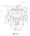
- FIGS. 1A and 1B provide an illustration of an apparatus 10 which is suitable for performing chamber cleaning using an internal energy source such as an in situ plasma or a thermal source or an external energy source respectively.
- the cleaning agent source 20 BCl 3 -depicted in FIG. 1A as solid arrows
- the reaction chamber 30 which has a residue 40 of metallic material to be removed.
- the residue 40 is deposited upon at least a portion of the exposed surface within the reaction chamber 30, particularly, the grounded sidewalls 32, showerhead 34, and work piece platform 36.
- the cleaning agent source 20 is exposed to an energy source 50, for example, an RF power supply or heater which converts the source, for example BCl 3 , of the cleaning agent to the cleaning agent 60, for example BCl, shown by the dashed arrows.
- the cleaning agent 60 reacts with residue 40 and forms a volatilized residue product 70.
- the volatilized residue product 70 is removed from the chamber 30 as shown by the dotted arrows.
- FIG. 1B provides an example of an apparatus 100 in which the cleaning agent source 120, for example BCl 3 , is exposed to an external energy source 150, for example a microwave source, to produce a high density plasma 110 of the cleaning agent within an applicator/resonant cavity 115.
- the high density plasma 110 can then be transported to the reaction chamber 130 containing the residue to form the volatilized residue product (not shown).
- the volatilized residue product can be removed readily from the chamber 130, aided by use of pump 160, via the foreline 140.
- Test coupons made of aluminum metal simulate the metal surface of the reaction chamber.
- Test coupons that are covered with an Al 2 O 3 film simulate a metallic material residue on the surface of a reaction chamber.
- the test coupons are placed on an RF-powered lower electrode in a modified parallel plate Gaseous Electronics Conference (GEC) reactor and exposed to a BCl plasma cleaning agent which is formed from BCL 3 .
- the plasma cleaning agent reacts with the Al 2 O 3 film and the aluminum metal of the test coupons to produce respectively a volatilized residue product (AlCl) and a volatilized metal (AlCl).
- Optical emission spectroscopy is used to monitor the presence of AlCl and BCl in the GEC reactor.
- Optical emission spectra (OES) are recorded in a capacitatively coupled BCl plasma.
- the plasma conditions are: 10 sccm (standard cubic centimeters, i.e. cm 3 at standard temperature and pressure) BCl 3 flow, 500 mTorr (67 Pa) chamber pressure, and 100 W RF power at 13.56 MHz.
- OES are recorded by an optical fiber coupled charge-coupled device (CCD) array spectrometer (Ocean Optics S2000).
- CCD charge-coupled device
- the OES peak which is associated with the presence of AlCl appears at the wavelength of 261 nm.
- the OES peak which is associated with the presence of BCl appears at the wavelength of 272 nm.
- the OES intensity which is representative of the amounts of AlCl and BCl present is given in arbitrary units.
- the OES of each of a test coupon coated with an Al 2 O 3 film and of an uncoated test coupon is compared.
- a test coupon coated with an Al 2 O 3 film by atomic layer deposition (ALD) is loaded into the GEC reactor.
- OES are recorded as the Al 2 O 3 film is removed from the surface of the coupon by the cleaning agent.
- an uncoated aluminum metal sample is loaded into the reactor.
- OES are recorded as the aluminum metal is etched by the BCl cleaning agent.
- OES are recorded also for BCl.
- Figure 2 shows an overlay of the OES from both runs to provide a comparison of peak intensities between the two runs for both AlCl and BCl.
- the spectrum indicated as the solid line represents the spectrum obtained in the first run with the test coupon coated with an Al 2 0 3 film.
- the spectrum indicated as the dotted line (---) represents the spectrum obtained in the second run with the uncoated aluminum metal test coupon.
- Table 1 lists the OES intensities and the intensity ratio between the AlCl emission at 261 nm and the BCl emission at 272 nm for these two runs. TABLE 1 Sample I(AlCl @261 @ 261 nm) I(BCl @ 272 nm) I(AlCl)(BCl) Al 2 O 3 2331 3458 0.67 Al 2983 2375 1.26
- the I(AlCl)/I(BCl) ratio is 0.67 when etching the Al 2 O 3 film and 1.26 when etching the aluminum metal sample.
- Some of the reactor internal components e.g. showerhead
- Some of the reactor internal components are made of aluminum alloy. This contributes to the baseline AlCl peak level in the data.
- the contrast in OES intensity ratio of I(AlCl)/I(BCl) will be more significant as the Al 2 O 3 residue is removed and the more reactive aluminum alloy is exposed to BCl plasma.
- the time evolution of I(AlCl) and I(BCl) and their ratio are measured to monitor the progression of a cleaning process.
- a test coupon coated with an Al 2 O 3 film is loaded into the reactor as described above.
- the plasma recipe is the same as for Example No. 1.
- OES is continuously recorded when the BCl plasma is turned on.
- Figure 3 shows the OES intensities I(AlCl) as a function of time (seconds).
- the BCl plasma cleaning agent removes the Al 2 O 3 film on the sample and the native Al 2 O 3 on surfaces of the internal aluminum components in the reactor.
- I(BCl) at 272 nm decreases and I(AlCl) at 261 nm increases.
- the ratio I(AlCl)/I(BCl) increases. This is shown as an inflection point in Figure 3 at approximately 90 seconds and represents the end point of the cleaning process.
- I(AlCl), I(BCl), and the ratio I(AlCl)/I(BCl) all reach a steady state.
- the change (or the turning point) in the intensity ratio I(AlCl)/I(BCl) will be more dramatic as the cleaning process approaches the endpoint.
- the usual data manipulation methods such as using the derivative of the intensity ratio I(AlCl)/I(BCl), can also be applied to locate the cleaning endpoint.
Applications Claiming Priority (1)
| Application Number | Priority Date | Filing Date | Title |
|---|---|---|---|
| US11/510,190 US20080047579A1 (en) | 2006-08-25 | 2006-08-25 | Detecting the endpoint of a cleaning process |
Publications (1)
| Publication Number | Publication Date |
|---|---|
| EP1892047A2 true EP1892047A2 (fr) | 2008-02-27 |
Family
ID=38754754
Family Applications (1)
| Application Number | Title | Priority Date | Filing Date |
|---|---|---|---|
| EP07114936A Withdrawn EP1892047A2 (fr) | 2006-08-25 | 2007-08-24 | Détection du point d'arret d'un procédé de nettoyage |
Country Status (5)
| Country | Link |
|---|---|
| US (1) | US20080047579A1 (fr) |
| EP (1) | EP1892047A2 (fr) |
| JP (1) | JP2008091882A (fr) |
| KR (1) | KR20080018810A (fr) |
| TW (1) | TW200811944A (fr) |
Cited By (1)
| Publication number | Priority date | Publication date | Assignee | Title |
|---|---|---|---|---|
| US11848178B2 (en) * | 2019-11-04 | 2023-12-19 | Applied Materials, Inc. | Optical absorption sensor for semiconductor processing |
Families Citing this family (6)
| Publication number | Priority date | Publication date | Assignee | Title |
|---|---|---|---|---|
| US8138482B2 (en) | 2008-05-23 | 2012-03-20 | Nano Green Technology, Inc. | Evaluating a cleaning solution using UV absorbance |
| US8445296B2 (en) * | 2011-07-22 | 2013-05-21 | Taiwan Semiconductor Manufacturing Company, Ltd. | Apparatus and methods for end point determination in reactive ion etching |
| US10724137B2 (en) * | 2013-02-05 | 2020-07-28 | Kokusai Eletric Corporation | Cleaning method, method of manufacturing semiconductor device, substrate processing apparatus, recording medium, and cleaning completion determining method |
| KR101885450B1 (ko) * | 2014-04-09 | 2018-08-03 | 가부시키가이샤 리코 | 클리닝 블레이드의 제조 방법, 클리닝 블레이드, 화상 형성 장치 및 프로세스 카트리지 |
| KR101700391B1 (ko) | 2014-11-04 | 2017-02-13 | 삼성전자주식회사 | 펄스 플라즈마의 고속 광학적 진단 시스템 |
| US10043641B2 (en) * | 2016-09-22 | 2018-08-07 | Applied Materials, Inc. | Methods and apparatus for processing chamber cleaning end point detection |
Family Cites Families (10)
| Publication number | Priority date | Publication date | Assignee | Title |
|---|---|---|---|---|
| US4182646A (en) * | 1978-07-27 | 1980-01-08 | John Zajac | Process of etching with plasma etch gas |
| US5846373A (en) * | 1996-06-28 | 1998-12-08 | Lam Research Corporation | Method for monitoring process endpoints in a plasma chamber and a process monitoring arrangement in a plasma chamber |
| US6534007B1 (en) * | 1997-08-01 | 2003-03-18 | Applied Komatsu Technology, Inc. | Method and apparatus for detecting the endpoint of a chamber cleaning |
| US6124927A (en) * | 1999-05-19 | 2000-09-26 | Chartered Semiconductor Manufacturing Ltd. | Method to protect chamber wall from etching by endpoint plasma clean |
| US20030221708A1 (en) * | 2002-06-04 | 2003-12-04 | Chun-Hao Ly | Method of cleaning a semiconductor process chamber |
| US7357138B2 (en) * | 2002-07-18 | 2008-04-15 | Air Products And Chemicals, Inc. | Method for etching high dielectric constant materials and for cleaning deposition chambers for high dielectric constant materials |
| US20040014327A1 (en) * | 2002-07-18 | 2004-01-22 | Bing Ji | Method for etching high dielectric constant materials and for cleaning deposition chambers for high dielectric constant materials |
| US20040011380A1 (en) * | 2002-07-18 | 2004-01-22 | Bing Ji | Method for etching high dielectric constant materials and for cleaning deposition chambers for high dielectric constant materials |
| US7479454B2 (en) * | 2003-09-30 | 2009-01-20 | Tokyo Electron Limited | Method and processing system for monitoring status of system components |
| US7055263B2 (en) * | 2003-11-25 | 2006-06-06 | Air Products And Chemicals, Inc. | Method for cleaning deposition chambers for high dielectric constant materials |
-
2006
- 2006-08-25 US US11/510,190 patent/US20080047579A1/en not_active Abandoned
-
2007
- 2007-08-20 KR KR1020070083332A patent/KR20080018810A/ko not_active Application Discontinuation
- 2007-08-21 TW TW096130952A patent/TW200811944A/zh unknown
- 2007-08-24 EP EP07114936A patent/EP1892047A2/fr not_active Withdrawn
- 2007-08-24 JP JP2007218421A patent/JP2008091882A/ja active Pending
Cited By (1)
| Publication number | Priority date | Publication date | Assignee | Title |
|---|---|---|---|---|
| US11848178B2 (en) * | 2019-11-04 | 2023-12-19 | Applied Materials, Inc. | Optical absorption sensor for semiconductor processing |
Also Published As
| Publication number | Publication date |
|---|---|
| US20080047579A1 (en) | 2008-02-28 |
| KR20080018810A (ko) | 2008-02-28 |
| JP2008091882A (ja) | 2008-04-17 |
| TW200811944A (en) | 2008-03-01 |
Similar Documents
| Publication | Publication Date | Title |
|---|---|---|
| US7055263B2 (en) | Method for cleaning deposition chambers for high dielectric constant materials | |
| KR100667723B1 (ko) | 고유전율 물질의 에칭 방법 및 고유전율 물질용 증착챔버의 세정 방법 | |
| KR100656770B1 (ko) | 고유전율 물질의 에칭 방법 및 고유전율 물질용 증착챔버의 세정 방법 | |
| US7371688B2 (en) | Removal of transition metal ternary and/or quaternary barrier materials from a substrate | |
| KR100887906B1 (ko) | 에칭 적용을 위한 고압력 웨이퍼리스 자동 세정 | |
| US20040011380A1 (en) | Method for etching high dielectric constant materials and for cleaning deposition chambers for high dielectric constant materials | |
| TWI713683B (zh) | 電漿處理方法 | |
| EP1840946A1 (fr) | Methode de nettoyage d'un dispositif de fabrication de semi-conducteurs et methode de gravure d'un substrat de silicium | |
| EP1892047A2 (fr) | Détection du point d'arret d'un procédé de nettoyage | |
| US20050241671A1 (en) | Method for removing a substance from a substrate using electron attachment | |
| US7479191B1 (en) | Method for endpointing CVD chamber cleans following ultra low-k film treatments | |
| JP2009050854A (ja) | 窒化チタンの除去方法 | |
| US7959970B2 (en) | System and method of removing chamber residues from a plasma processing system in a dry cleaning process | |
| EP1619267A2 (fr) | Procédé pour enlever des résidus carbonnés d'un substrat | |
| JPH05267256A (ja) | 反応室の洗浄方法 | |
| US20060189171A1 (en) | Seasoning process for a deposition chamber | |
| EP1764848A2 (fr) | Méthode d'élimination de composés organiques électroluminescents d'un substrate | |
| EP1724374A1 (fr) | Procédé pour nettoyer des pièces d'outillage par un gaz réactif | |
| JP2008060171A (ja) | 半導体処理装置のクリーニング方法 | |
| Li et al. | Surface chemical changes of aluminum during NF 3-based plasma processing used for in situ chamber cleaning | |
| Dictus et al. | Impact of metal etch residues on etch species density and uniformity |
Legal Events
| Date | Code | Title | Description |
|---|---|---|---|
| PUAI | Public reference made under article 153(3) epc to a published international application that has entered the european phase |
Free format text: ORIGINAL CODE: 0009012 |
|
| AK | Designated contracting states |
Kind code of ref document: A2 Designated state(s): AT BE BG CH CY CZ DE DK EE ES FI FR GB GR HU IE IS IT LI LT LU LV MC MT NL PL PT RO SE SI SK TR |
|
| AX | Request for extension of the european patent |
Extension state: AL BA HR MK YU |
|
| STAA | Information on the status of an ep patent application or granted ep patent |
Free format text: STATUS: THE APPLICATION HAS BEEN WITHDRAWN |
|
| 18W | Application withdrawn |
Effective date: 20081103 |