EP1890145A1 - Wechselwirkungsnachweiseinheit mit elektrode des gleichen potentials, sensorchip unter verwendung der nachweiseinheit und wechselwirkungsnachweisvorrichtung - Google Patents
Wechselwirkungsnachweiseinheit mit elektrode des gleichen potentials, sensorchip unter verwendung der nachweiseinheit und wechselwirkungsnachweisvorrichtung Download PDFInfo
- Publication number
- EP1890145A1 EP1890145A1 EP06732552A EP06732552A EP1890145A1 EP 1890145 A1 EP1890145 A1 EP 1890145A1 EP 06732552 A EP06732552 A EP 06732552A EP 06732552 A EP06732552 A EP 06732552A EP 1890145 A1 EP1890145 A1 EP 1890145A1
- Authority
- EP
- European Patent Office
- Prior art keywords
- interaction
- electrode
- electric field
- reaction region
- electrodes
- Prior art date
- Legal status (The legal status is an assumption and is not a legal conclusion. Google has not performed a legal analysis and makes no representation as to the accuracy of the status listed.)
- Withdrawn
Links
Images


Classifications
-
- G—PHYSICS
- G01—MEASURING; TESTING
- G01N—INVESTIGATING OR ANALYSING MATERIALS BY DETERMINING THEIR CHEMICAL OR PHYSICAL PROPERTIES
- G01N33/00—Investigating or analysing materials by specific methods not covered by groups G01N1/00 - G01N31/00
- G01N33/48—Biological material, e.g. blood, urine; Haemocytometers
- G01N33/50—Chemical analysis of biological material, e.g. blood, urine; Testing involving biospecific ligand binding methods; Immunological testing
- G01N33/53—Immunoassay; Biospecific binding assay; Materials therefor
- G01N33/543—Immunoassay; Biospecific binding assay; Materials therefor with an insoluble carrier for immobilising immunochemicals
- G01N33/54366—Apparatus specially adapted for solid-phase testing
- G01N33/54373—Apparatus specially adapted for solid-phase testing involving physiochemical end-point determination, e.g. wave-guides, FETS, gratings
- G01N33/5438—Electrodes
-
- B—PERFORMING OPERATIONS; TRANSPORTING
- B01—PHYSICAL OR CHEMICAL PROCESSES OR APPARATUS IN GENERAL
- B01L—CHEMICAL OR PHYSICAL LABORATORY APPARATUS FOR GENERAL USE
- B01L3/00—Containers or dishes for laboratory use, e.g. laboratory glassware; Droppers
- B01L3/50—Containers for the purpose of retaining a material to be analysed, e.g. test tubes
- B01L3/502—Containers for the purpose of retaining a material to be analysed, e.g. test tubes with fluid transport, e.g. in multi-compartment structures
- B01L3/5027—Containers for the purpose of retaining a material to be analysed, e.g. test tubes with fluid transport, e.g. in multi-compartment structures by integrated microfluidic structures, i.e. dimensions of channels and chambers are such that surface tension forces are important, e.g. lab-on-a-chip
-
- C—CHEMISTRY; METALLURGY
- C12—BIOCHEMISTRY; BEER; SPIRITS; WINE; VINEGAR; MICROBIOLOGY; ENZYMOLOGY; MUTATION OR GENETIC ENGINEERING
- C12Q—MEASURING OR TESTING PROCESSES INVOLVING ENZYMES, NUCLEIC ACIDS OR MICROORGANISMS; COMPOSITIONS OR TEST PAPERS THEREFOR; PROCESSES OF PREPARING SUCH COMPOSITIONS; CONDITION-RESPONSIVE CONTROL IN MICROBIOLOGICAL OR ENZYMOLOGICAL PROCESSES
- C12Q1/00—Measuring or testing processes involving enzymes, nucleic acids or microorganisms; Compositions therefor; Processes of preparing such compositions
- C12Q1/68—Measuring or testing processes involving enzymes, nucleic acids or microorganisms; Compositions therefor; Processes of preparing such compositions involving nucleic acids
- C12Q1/6813—Hybridisation assays
- C12Q1/6834—Enzymatic or biochemical coupling of nucleic acids to a solid phase
- C12Q1/6837—Enzymatic or biochemical coupling of nucleic acids to a solid phase using probe arrays or probe chips
-
- G—PHYSICS
- G01—MEASURING; TESTING
- G01N—INVESTIGATING OR ANALYSING MATERIALS BY DETERMINING THEIR CHEMICAL OR PHYSICAL PROPERTIES
- G01N21/00—Investigating or analysing materials by the use of optical means, i.e. using sub-millimetre waves, infrared, visible or ultraviolet light
- G01N21/75—Systems in which material is subjected to a chemical reaction, the progress or the result of the reaction being investigated
- G01N21/77—Systems in which material is subjected to a chemical reaction, the progress or the result of the reaction being investigated by observing the effect on a chemical indicator
- G01N21/78—Systems in which material is subjected to a chemical reaction, the progress or the result of the reaction being investigated by observing the effect on a chemical indicator producing a change of colour
-
- G—PHYSICS
- G01—MEASURING; TESTING
- G01N—INVESTIGATING OR ANALYSING MATERIALS BY DETERMINING THEIR CHEMICAL OR PHYSICAL PROPERTIES
- G01N27/00—Investigating or analysing materials by the use of electric, electrochemical, or magnetic means
- G01N27/26—Investigating or analysing materials by the use of electric, electrochemical, or magnetic means by investigating electrochemical variables; by using electrolysis or electrophoresis
- G01N27/416—Systems
- G01N27/447—Systems using electrophoresis
- G01N27/44704—Details; Accessories
- G01N27/44717—Arrangements for investigating the separated zones, e.g. localising zones
- G01N27/4473—Arrangements for investigating the separated zones, e.g. localising zones by electric means
-
- G—PHYSICS
- G01—MEASURING; TESTING
- G01N—INVESTIGATING OR ANALYSING MATERIALS BY DETERMINING THEIR CHEMICAL OR PHYSICAL PROPERTIES
- G01N33/00—Investigating or analysing materials by specific methods not covered by groups G01N1/00 - G01N31/00
- G01N33/48—Biological material, e.g. blood, urine; Haemocytometers
- G01N33/50—Chemical analysis of biological material, e.g. blood, urine; Testing involving biospecific ligand binding methods; Immunological testing
- G01N33/53—Immunoassay; Biospecific binding assay; Materials therefor
- G01N33/5302—Apparatus specially adapted for immunological test procedures
Definitions
- the present invention relates to a technique for detecting an interaction between materials. More specifically, the invention relates to a technique for detecting an interaction between materials by utilizing an electrodynamic action.
- a DNA chip in which predetermined DNAs are finely arranged by utilizing a microarray technique has been utilized for an analysis of mutation of a gene, an analysis of SNPs (single nucleotide polymorphisms), an analysis of a frequency of genomic expression, and the like.
- the DNA chip begins to be generally used in the fields of a drug discovery, a clinical diagnosis, a pharmacogenomics, a research of evolution, a forensic medicine, and the others.
- DNA chip an exhaustive analysis of a hybridization becomes possible because the various and multiple DNA oligo chains or nucleotide chains such as a complementary DNA (cDNA) are integrated on a glass substrate or a silicon substrate.
- a sensor chip for example, a protein chip
- detecting an interaction between biologic molecules other than nucleic acid molecules or a detector is variously developed.
- Japanese Patent Laid-Open No. 2001-330608 discloses a technique that a nucleic acid probe template chain immobilized on a template substrate is used to synthesize a nucleic acid probe chain along the template chain, and the synthesized probe chain is immobilized on another array substrate by utilizing an electric field, thereby simply manufacturing a nucleic acid chain immobilized array at a low cost.
- Japanese Patent Laid-Open No. 2001-242135 discloses a technique that a chip for detection is composed of a main body portion and a frame which are detachable from each other, a large number of pin electrodes are protruded in matrix inside the main body portion, oligonucleotide composed of different gene sequences is immobilized on the pin electrodes, a common electrode is disposed in a hollow of the frame so as not to contact any of the pin electrodes, a voltage is applied across the common electrode and each of the pin electrodes, thereby detecting a double-strained DNA obtained through a hybridization by detecting a current.
- Japanese Patent Laid-Open No. 2004-135512 discloses a hybridization detecting portion structured such that a reaction region becoming a field for a hybridization between a nucleotide chain for detection and a target nucleotide chain having a base sequence complementary to the nucleotide chain for detection can be fixedly fastened to an end portion of a scanning electrode through an action of a dielectrophoresis while the nucleotide chain for detection is elongated by application of an electric field.
- each of the prior arts described above utilizes the electrode or a group of electrodes which is disposed so as to face the reaction region. Therefore, each of the prior arts described above involves a technical problem that it is difficult to exert the desired electrodynamic effect on the entire reaction region because the electric field (electric lines of force) is generated across the counter electrodes.
- reaction region in the sensor chip such as the DNA chip or the protein chip is generally limited.
- the electrode or the group of electrodes showing the counter disposition relationship with the reaction region are provided, there are encountered technical problems: (1) The structure of the reaction region becomes more complicated, (2) the morphologic restriction to the reaction region occurs because of the formation of the counter electrode, (3) the number of processes for manufacturing the chip increases, (4) the distribution- of the electric supply line to the electrodes is also complicated, and so forth.
- the present invention firstly provides an interaction detecting portion including at least a reaction region for providing a field for an interaction between materials, and an electrode or a group of electrodes, having the same potential, which is provided so as to face the reaction region, and a sensor chip including at least one interaction detecting portion concerned.
- An A.C. electric field for example, is adopted as an electric field applied to the electrode or the group of electrodes, thereby obtaining a desired electrodynamic effect such as a dielectrophoresis.
- the electrode or the group of electrodes has an irregular shape in its surface makes it possible to form a nonuniform electric field in the irregular shape, especially, in the vicinity of a stepped portion. An action of the dielectrophoresis can be efficiently obtained in a region in which the nonuniform electric field is formed.
- the surface of the electrode or the group of electrodes is covered with an insulating layer, thereby making it possible to prevent an electrochemical reaction from occurring due to an ion solution which is accumulated in the reaction region in some cases.
- the present invention provides an interaction detector including at least a reaction region for providing a field for an interaction between materials, an electrode or a group of electrodes, having the same potential, which is provided so as to face the reaction region, and means for applying an electric field to the electrode or the group of electrodes.
- Means for applying an A.C. electric field across the electrode or the group of electrodes, and a grounding portion, for example, can be adopted as the electric field applying means constituting the interlayer detector.
- the electric field applying means can also apply a high frequency electric field to the electrode or the group of electrodes through an impedance matching circuit.
- the electrodynamic action such as the dielectrophoresis is given to the material existing in the reaction region by application of the electric field.
- the interaction generally means a chemical bond or dissociation containing a noncovalent bond, a covalent bond and a hydrogen bond between materials.
- the interaction generally contains the hybridization between nucleic acid molecules, the interaction between protein materials, and the chemical bond or dissociation, between materials, such as an antigen-antibody complex reaction.
- the hybridization means a complementary strand (duplex) forming reaction, between materials, having a complementary base sequence structure.
- the nucleic acid chain means a polymer (nucleotide chain) of phosphate ester of nucleoside obtained by glycosidically bonding a purine or pyrimidine base and sugar to each other.
- the nucleic acid chain generally contains a DNA (an entire length or a fragment) obtained by polymerizing oligonucleotide containing a prove DNA, a polynucleotide, purinenucleotide, and pyrimidinenucleotide, a cDNA (c prove DNA) obtained through reverse transcription, an RNA, a polyamidenucleotide derivative (PNA), and the like.
- the reaction region is a region in which the field for the interaction such as the hybridization can be provided.
- a reaction field, having a well shape, in which a liquid phase material or a gel can be accumulated is given as an example of "the reaction region”.
- the dielectrophoresis is a phenomenon that molecules are driven to a stronger electric field in a field having a nonuniform electric field. Even when the A.C. voltage is applied to the molecules, the driving effect can be obtained similarly to the case of application of the D.C. voltage because the polarity of the polarization is also inversed along with inversion of the polarity of the applied voltage (refer to a literature of " Micro Machine and Materials (published by CMC Publishing Co., Ltd.)" complied under the super vision of Teru Hayashi, Manipulation of Cells and DNAs (Fifth Chapter), pp.37 to 46 ). In particular, the force acts on the dipoles of the molecules in proportion to a gradient of a square of a time average electric field within the high frequency A.C. electric field, so that the molecules migrate.
- the nucleic acid molecules when receiving the action of the electric field exerted thereon in the liquid phase, the nucleic acid molecules elongate or move.
- phosphoric acid ions negative electric charges
- hydrogen atoms positive electric charges
- the polarization vectors (dipoles) generated from the negative electric charges and the positive electric charges are oriented to one direction as a whole by application of the high voltage having a high frequency to elongate.
- the sensor chip means a substrate for causing an interaction between materials to progress, and detecting the interaction between the materials in a predetermined reaction region on the substrate.
- the sensor chip generally includes such substrates irrespective of the kind of material, and the principles for detecting the interaction is not subject matter in the sensor chip.
- the sensor chip at least includes the DNA chip (DNA microarray) in which the nucleic acid chains such as the DNA probe is immobilized on the substrate to become a state of being finely arranged, the protein chip which is suitable for detecting the interaction between the protein materials, and the antigen-antibody complex reaction or the like, and the like.
- the present invention adopts the structure that the electrode (that is, the counter electrode) disposed so as to face the reaction region is not provided, but the electrode or the group of electrodes having the same potential is provided.
- the applied electric field electric lines of force
- the electric field electric lines of force
- the electrical gradient, or the nonuniform electric field can be formed in the entire reaction region.
- the materials dispersed in the reaction region can be efficiently collected up in larger numbers to the electrode side through the electrodynamic migration action.
- the structure of the detection portion can be simplified.
- the grounding portion has to be previously connected to the system side, and the wiring for the detection portion has to be connected to only the electrode in the hybridization region.
- the structure of the detector can also be simplified.
- FIG. 1 is a main portion cubic perspective view explaining a basic constitution of a first embodiment as an interaction detecting portion (hereinafter referred to as "a detection portion") according to the present invention
- FIG. 2 is a transverse cross sectional view of the detection portion
- FIG. 3 is a cross sectional view taken on line A - A of FIG. 2 .
- FIGS. 1 to 3 show the preferred first embodiment of the detection portion 1 according to the present invention.
- a reaction region 2 having a well shape (inverse recess shape) in which a medium such as a solution or a gel can be accumulated or held is provided in the detection portion 1.
- the reaction region 2 functions as a region or a space for providing a field for an interaction, such as a hybridization, between materials.
- An A.C. electric field for example, is applied to the medium accumulated or held in the reaction region 2 through an electrode E 1 which is formed so as to face the reaction region 2.
- the electrode E 1 is made of either a metal such as aluminum or gold, or a transparent conductor such as ITO (indium-tin-oxide).
- the electrode E 1 is disposed at a central position of a bottom surface-21 of the reaction region 2. It is noted that the place where the electrode E 1 is formed is not limited to the bottom surface 21.
- the electrode E 1 may also be formed either in an upper side substrate 5 or in a position of a spacer 6 which will be described later so as to face the reaction region 2.
- the electrode E 1 is desirably covered with an insulating layer 3 made of a material which is selected from among SiO 2 , SiC, SiN, SiOC, SiOF, TiO 2 , and the like.
- an insulating layer 3 made of a material which is selected from among SiO 2 , SiC, SiN, SiOC, SiOF, TiO 2 , and the like. The reason for this is because an electrochemical reaction is prevented from occurring due to an ion solution which is accumulated in the reaction region 2 in some cases.
- a surface of the electrode E 1 can be operated as a detection surface on which a material D to be detected such as a DNA probe is immobilized. More specifically, surface processing for allowing the end of the material D to be detected such as the probe DNA to be immobilized is previously executed for the electrode E 1 .
- the material D to be detected can be immobilized on the surface of the electrode E 1 based on a coupling reaction or the like occurring between the surface of the electrode E 1 and the end of the probe DNA (an example of the material D to be detected).
- a coupling reaction or the like occurring between the surface of the electrode E 1 and the end of the probe DNA (an example of the material D to be detected).
- the electrode surface for which the surface processing is executed by using streptavidin it is suitable for immobilizing the end of the biotinylated material D to be detected.
- a thiol (SH) group it is suitable for immobilizing the material D to be detected, such as the probe DNA, having the end modified with the thiol group by using a disulfide bond (-S-S-bond).
- reference symbols D and T shown in each of FIG. 1 and the like schematically designate the material to be- detected, typified by the DNA probe, having the end immobilized on the surface of the electrode E 1 , and a target material showing a specific interaction with the material D to be detected, respectively.
- reference symbol W shown in FIGS. 2 and 3 designates a complex (for example, a double-stranded nucleic acid) which is formed based on a specific interaction (for example, a hybridization) between the material D to be detected and the target material T.
- Reference numerals 4 and 5 shown in each of FIGS. 1 to 3 designate substrates, respectively.
- the substrate 4, for example, is an optically-transparent substrate with which recorded information (interaction information in the present invention) within the reaction region can be optically read out, and for example, is made of a quartz glass or silicon, or a synthetic resin such as polycarbonate, polystyrene or polyolefin.
- the substrate designated with reference numeral 5 functions as a cover which closes the reaction region 2, and may be made of the same base material as that of the substrate 4, or may be made of a material having a light reflecting function in accordance with the intended use.
- Reference numeral 6 shown in each of FIG. 6 and the like designates a spacer member made of an insulating material such as SiO 2 or a synthetic resin. It is noted that this spacer member 6 may be formed either separately from the substrate 4 or 5, or integrally with the substrate 4 or 5. When the spacer member 6 is formed integrally with the substrate 4 or 5, the reaction region 2 which plays a role for presenting a field for the interaction such as the hybridization can be formed by utilizing the known optical disc mastering technique.
- a structure is adopted in which a voltage can be applied from a power source V such as an A.C. power source across the electrode E 1 and a grounding portion 7 provided outside the reaction region 2 in accordance with an operation for turning ON/OFF a switch S (electric field applying means).
- a power source V such as an A.C. power source across the electrode E 1 and a grounding portion 7 provided outside the reaction region 2 in accordance with an operation for turning ON/OFF a switch S (electric field applying means).
- the structure of the reaction region 2 can be simplified. Moreover, when the electric field is applied thereacross, with respect to the wiring itself, the grounding portion has to be previously connected to the system side, and the wiring to the detection portion has to be connected to only the electrode E 1 within the reaction region 2. As a result, the structure of the detector (for detecting the hybridization and a signal) can also be simplified.
- the electric field concentrates on the vicinity of the electrode E 1 , so that the nonuniform electric field can be formed.
- the electrode structure suitable for generating the nonuniform electric field while not especially illustrated, it is expected that the surface of the electrode E 1 , for example, is subjected to rough surfacing processing so as to obtain an irregular shape, or is patterned so as to obtain an island-like shape, thereby causing the electric field to be easy to concentrate on a convex portion (angled portion) of the surface of the electrode E 1 concerned.
- the electric field can be especially caused to concentrate on a corner portion of the convex portion, a bend portion of a recess portion, or the like.
- the action and effect of the dielectrophoresis can be more reliably utilized in the region in the vicinity of the electrode E 1 .
- the method of subjecting the electrode surface to the rough surfacing processing can be carried out by, for example, utilizing the known sputter depositing technique, epitaxy depositing technique or etching technique, it is not especially limited.
- the material which dispersively exists in the reaction region 2 described above at random can be drawn near the electrode E 1 side or can be elongated in a direction along the electric field due to the electrodynamic action such as the dielectrophoresis.
- the strength, frequency, and an application period of time of the applied electric field are not especially limited.
- the proper electric field strength, frequency, and application period of time of the applied electric field are desirably selected in accordance with the kind, the molecular length and the like of the object to which the electric field is applied.
- the waveform of the applied electric field is not also limited to the sine wave, and thus for example, may be a chopping wave or the like.
- an impedance matching circuit 8 is provided between the electrode E 1 and the power source V to obtain the impedance matching between them, so that the power can be efficiently supplied to the electrode E 1 .
- FIG. 4 simply shows an example of a circuit structure of the impedance matching circuit 8.
- the impedance matching circuit 8 is provided between the grounded power source V and the grounded detection portion 1.
- the impedance matching circuit 8 includes two variable capacitors C 1 and C 2 which are grounded, and an inductance neutralizing circuit (neutralization coil) L n , as a neutralization element, which is interposed between the two variable capacitors C 1 and C 2 .
- the two variable capacitors C 1 and C 2 play a role for adjusting a capacitance
- the inductance neutralizing circuit L n plays a role for adjusting an inductance.
- FIG. 5 a more detailed constitution of a preferred embodiment of the electric field applying means is shown in the form of a block diagram in FIG. 5 .
- a signal outputted from the grounded power source (that is, the signal generating source) V is amplified by an amplifier 81 connected to the grounded power source V and is taken out in the form of an output signal. Also, a transmission wave W t about the resulting output signal is inputted and detected by a signal detector (sensor) 83 through a directional coupler designated with reference numeral 82. Also, an output power of the output signal thus detected is measured by a measuring instrument 84. A control portion 85 monitors this measured value.
- a reflected wave W r from the electrode E 1 located at a termination is detected by the signal detector (sensor) 86 through the directional coupler 82, and a reflected power thereof is measured by a measuring instrument 87.
- the control portion 85 monitors this measured value.
- the impedance matching circuit 8 adjusts a magnitude of the internal impedance Z v of the power source, and a magnitude of the load impedance Z e of the counter electrode E 1 in accordance with a control signal C which the control portion 85 outputs based on the measured value described above (refer to FIG. 5 ).
- the loss of the power supplied from the power source V to the counter electrode E 1 is reduced, so that the supplied power becomes maximum by utilizing the technique for exerting the electrodynamic action on the material existing in the reaction region 2 of the detection portion 1, for example, the nucleic acid molecules.
- the nucleic acid chain concerned receives the electrodynamic action of the dielectrophoresis to migrate toward the electrode E 1 having the stronger electric field strength.
- the target nucleic acid chains are collected on the surface of the electrode E 1 on which the nucleic acid chains such as the probe DNA functioning as the material D to be detected are previously immobilized, so that the hybridization efficiently progresses.
- the target nucleic acid chains are moved to the surface of the electrode E 1 for a short period of time through the dielectrophosresis described above to increase the concentration thereof, which results in that a period of time required for the hybridization with the nucleic acid chains immobilized on the surface of the electrode E 1 can be greatly shortened.
- a quantity of light emitted from an intercalate which is specifically bonded to the double strand (double stranded nucleic acid) may be measured, a quantity of light emitted from a fluorescence dye which is previously bonded to the target DNA may be measured after the excessive DNAs are removed after completion of the hybridization.
- a quantity of emitted light following the hybridization reaction may be measured by utilizing a molecular beacon.
- FIG. 6 is a cross sectional view (a cross sectional view common to FIG. 2 ) in which a situation of applying the electric field to the reaction region 2 is schematically shown by using the electric lines of force.
- the electric field is formed from the electrode E 1 having no counter electrode toward the entire reaction region 2.
- the desired electrodynamic action such as the dielectrophoresis can be exerted on the entire reaction region 2.
- the electric field (electric lines of force) can be made to diverge extensively toward the entire reaction region, the electrical gradient or the nonuniform electric field can be formed throughout the reaction region 2.
- the material dispersed in the reaction region 2 can be efficiently collected up in larger numbers on the electrode E 1 side based on the electrodynamic migration action.
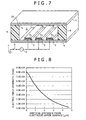
- FIG. 7 is a view showing a second embodiment of a detection portion according to the present invention.
- the detection portion 10 as the second embodiment includes three electrodes E 1 , E 2 and E 3 having the same potential.
- the number of electrodes having the same potential may be two, or three or more. Also, it is also free that a plurality of electrodes are disposed on the upper surface of the substrate 4, or the like in various patterns.
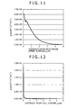
- FIGS. 8 , 9 and 10 show the distributions of the electric field strength in a vertical direction, in an oblique direction, and in a horizontal direction, respectively, in the case where the A.C. electric field obtained from ⁇ 20 V of 1 MHz is applied across the electrode E 1 and the ground on the assumption that the grounding portion is provided at infinity in the electrode E 1 having a diameter of 10 ⁇ m provided in the reaction region which is 100 ⁇ m in diameter and 5 ⁇ m in height.
- FIGS. 11, 12 and 13 show distributions of the percentage changes of the electric field strength (the gradients of squares of the electric field strength) in the vertical direction, in the oblique direction and in the horizontal direction, respectively.
- FIG. 14 is a drawing substitution data table showing electric field strength data (right-hand side) and numerical data (left-hand side) on differential calculus of a square of electric field strength with respect to distances (unit: ⁇ m) in the vertical direction, in the oblique direction, and in the horizontal direction, respectively.
- FIG. 15 is a view showing concepts of the vertical direction (Z), the horizontal direction (H), and the oblique direction (R) with respect to the distributions of the electric field strength in the periphery of the electrode.
- the present invention can be utilized as the technique for detecting efficiently and precisely the interaction between the materials for a short period of time by utilizing the electrodynamic action. Also, the present invention can be utilized as the technique for the sensor chip typified by the DNA chip or the protein chip, or as the apparatus for detecting the interaction.
Applications Claiming Priority (2)
| Application Number | Priority Date | Filing Date | Title |
|---|---|---|---|
| JP2005164591A JP2006337273A (ja) | 2005-06-03 | 2005-06-03 | 同一電位の電極を備える相互作用検出部と該検出部を用いるセンサーチップ、並びに相互作用検出装置 |
| PCT/JP2006/309571 WO2006129464A1 (ja) | 2005-06-03 | 2006-05-12 | 同一電位の電極を備える相互作用検出部と該検出部を用いるセンサーチップ、並びに相互作用検出装置 |
Publications (2)
| Publication Number | Publication Date |
|---|---|
| EP1890145A1 true EP1890145A1 (de) | 2008-02-20 |
| EP1890145A4 EP1890145A4 (de) | 2008-10-29 |
Family
ID=37481395
Family Applications (1)
| Application Number | Title | Priority Date | Filing Date |
|---|---|---|---|
| EP06732552A Withdrawn EP1890145A4 (de) | 2005-06-03 | 2006-05-12 | Wechselwirkungsnachweiseinheit mit elektrode des gleichen potentials, sensorchip unter verwendung der nachweiseinheit und wechselwirkungsnachweisvorrichtung |
Country Status (6)
| Country | Link |
|---|---|
| US (1) | US20100213056A1 (de) |
| EP (1) | EP1890145A4 (de) |
| JP (1) | JP2006337273A (de) |
| KR (1) | KR20080016825A (de) |
| CN (1) | CN101189517A (de) |
| WO (1) | WO2006129464A1 (de) |
Families Citing this family (6)
| Publication number | Priority date | Publication date | Assignee | Title |
|---|---|---|---|---|
| CN102384980B (zh) * | 2010-08-30 | 2014-03-26 | 明达医学科技股份有限公司 | 微流体操控装置及其操作方法 |
| CN102478581A (zh) * | 2010-11-29 | 2012-05-30 | 中国科学院沈阳自动化研究所 | 基于聚3-己基噻吩和c60衍生物的光敏混合聚合物光电导薄膜操控芯片及制备方法 |
| KR101646182B1 (ko) * | 2014-03-25 | 2016-08-05 | 울산과학기술원 | 바이오 센서 |
| KR101727107B1 (ko) * | 2016-02-19 | 2017-04-17 | 한국과학기술연구원 | 유전체 전기영동을 이용한 마이크로 전극 바이오 센서 |
| TWI745392B (zh) * | 2017-06-29 | 2021-11-11 | 瑞禾生物科技股份有限公司 | 生物感測元件及其製造方法以及生物分子檢測方法 |
| US11005622B2 (en) * | 2017-12-28 | 2021-05-11 | Qualcomm Incorporated | Reference signal sequence design for new radio systems |
Citations (1)
| Publication number | Priority date | Publication date | Assignee | Title |
|---|---|---|---|---|
| US20050069932A1 (en) * | 2003-09-25 | 2005-03-31 | Fujitsu Limited | Analyte evaluating device, and method for evaluating analyte |
Family Cites Families (5)
| Publication number | Priority date | Publication date | Assignee | Title |
|---|---|---|---|---|
| JP3734131B2 (ja) | 1999-03-01 | 2006-01-11 | 松下電器産業株式会社 | 微生物数測定装置および微生物数測定方法 |
| JP2003028801A (ja) * | 2001-07-13 | 2003-01-29 | Matsushita Electric Ind Co Ltd | モニタリング方法 |
| JP4039201B2 (ja) | 2002-08-20 | 2008-01-30 | ソニー株式会社 | ハイブリダイゼーション検出部とセンサーチップ及びハイブリダイゼーション方法 |
| JP2005114427A (ja) | 2003-10-03 | 2005-04-28 | Sony Corp | 二枚の基板を重ね合わせてバイオアッセイ用基板を製造する方法及びバイオアッセイ用基板 |
| JP4411931B2 (ja) * | 2003-10-23 | 2010-02-10 | ソニー株式会社 | 物質間の相互作用検出方法 |
-
2005
- 2005-06-03 JP JP2005164591A patent/JP2006337273A/ja not_active Abandoned
-
2006
- 2006-05-12 KR KR1020077028003A patent/KR20080016825A/ko not_active Application Discontinuation
- 2006-05-12 WO PCT/JP2006/309571 patent/WO2006129464A1/ja active Application Filing
- 2006-05-12 EP EP06732552A patent/EP1890145A4/de not_active Withdrawn
- 2006-05-12 US US11/916,206 patent/US20100213056A1/en not_active Abandoned
- 2006-05-12 CN CNA200680019723XA patent/CN101189517A/zh active Pending
Patent Citations (1)
| Publication number | Priority date | Publication date | Assignee | Title |
|---|---|---|---|---|
| US20050069932A1 (en) * | 2003-09-25 | 2005-03-31 | Fujitsu Limited | Analyte evaluating device, and method for evaluating analyte |
Non-Patent Citations (1)
| Title |
|---|
| See also references of WO2006129464A1 * |
Also Published As
| Publication number | Publication date |
|---|---|
| CN101189517A (zh) | 2008-05-28 |
| WO2006129464A1 (ja) | 2006-12-07 |
| EP1890145A4 (de) | 2008-10-29 |
| KR20080016825A (ko) | 2008-02-22 |
| JP2006337273A (ja) | 2006-12-14 |
| US20100213056A1 (en) | 2010-08-26 |
Similar Documents
| Publication | Publication Date | Title |
|---|---|---|
| EP1605063B1 (de) | Detektionseinheit für Hybridisierungen, sowie DNA-Chip umfassend die Detektionseinheit | |
| US20100163414A1 (en) | Microelectronic device with field electrodes | |
| EP2165353B1 (de) | Systeme und verfahren zur elektronischen erkennung mit nanofets | |
| JP4328168B2 (ja) | 毛細管現象を利用する物質間の相互作用検出部と該検出部を用いる方法及びバイオアッセイ用基板 | |
| US7709195B2 (en) | Hybridization detecting unit relying on dielectrophoresis and sensor chip provided with the detecting unit | |
| EP1890145A1 (de) | Wechselwirkungsnachweiseinheit mit elektrode des gleichen potentials, sensorchip unter verwendung der nachweiseinheit und wechselwirkungsnachweisvorrichtung | |
| CN113967488B (zh) | 微流体分析设备 | |
| JP4039201B2 (ja) | ハイブリダイゼーション検出部とセンサーチップ及びハイブリダイゼーション方法 | |
| JP4321854B2 (ja) | ハイブリダイゼーションその他の相互作用検出部と該検出部を備えるdnaチップその他のバイオアッセイ用基板 | |
| EP1677110A1 (de) | Verfahren zur hestellung eines bioassay-substrats durch übereinanderlegen von zwei substraten und bioassay-substrat | |
| JP2005345353A (ja) | 蛍光励起光の遮光層を備えるバイオアッセイ用基板 | |
| JP4411931B2 (ja) | 物質間の相互作用検出方法 | |
| EP1520628A1 (de) | Detektion von Interaktionen zwischen Substanzen | |
| JP4631543B2 (ja) | 物質間の相互作用検出部と該検出部を用いるセンサーチップ、並びに電界を用いるバイオアッセイ方法 | |
| US20060127904A1 (en) | Hybridization sensing part, sensor chip, and hybridization method | |
| JP4367441B2 (ja) | ハイブリダイゼーション方法 | |
| JP2004132720A (ja) | ハイブリダイゼーション検出部とセンサーチップ及びハイブリダイゼーション方法 | |
| JP2005341913A (ja) | インピーダンスマッチングを利用するハイブリダイゼーション検出装置及び検出方法。 | |
| US20100056388A1 (en) | Nucleic acid array having fixed nucleic acid anti-probes and complementary free nucleic acid probes | |
| JP2006337065A (ja) | 物質間の相互作用するバイオアッセイ用基板と相互作用検出装置 |
Legal Events
| Date | Code | Title | Description |
|---|---|---|---|
| PUAI | Public reference made under article 153(3) epc to a published international application that has entered the european phase |
Free format text: ORIGINAL CODE: 0009012 |
|
| 17P | Request for examination filed |
Effective date: 20071015 |
|
| AK | Designated contracting states |
Kind code of ref document: A1 Designated state(s): DE FR GB |
|
| DAX | Request for extension of the european patent (deleted) | ||
| RBV | Designated contracting states (corrected) |
Designated state(s): DE FR GB |
|
| A4 | Supplementary search report drawn up and despatched |
Effective date: 20080925 |
|
| 17Q | First examination report despatched |
Effective date: 20081121 |
|
| STAA | Information on the status of an ep patent application or granted ep patent |
Free format text: STATUS: THE APPLICATION IS DEEMED TO BE WITHDRAWN |
|
| 18D | Application deemed to be withdrawn |
Effective date: 20091120 |