EP1887683A1 - Three level power converter - Google Patents
Three level power converter Download PDFInfo
- Publication number
- EP1887683A1 EP1887683A1 EP06731430A EP06731430A EP1887683A1 EP 1887683 A1 EP1887683 A1 EP 1887683A1 EP 06731430 A EP06731430 A EP 06731430A EP 06731430 A EP06731430 A EP 06731430A EP 1887683 A1 EP1887683 A1 EP 1887683A1
- Authority
- EP
- European Patent Office
- Prior art keywords
- switching device
- switching
- diodes
- switching devices
- devices
- Prior art date
- Legal status (The legal status is an assumption and is not a legal conclusion. Google has not performed a legal analysis and makes no representation as to the accuracy of the status listed.)
- Granted
Links
Images




Classifications
-
- H—ELECTRICITY
- H02—GENERATION; CONVERSION OR DISTRIBUTION OF ELECTRIC POWER
- H02M—APPARATUS FOR CONVERSION BETWEEN AC AND AC, BETWEEN AC AND DC, OR BETWEEN DC AND DC, AND FOR USE WITH MAINS OR SIMILAR POWER SUPPLY SYSTEMS; CONVERSION OF DC OR AC INPUT POWER INTO SURGE OUTPUT POWER; CONTROL OR REGULATION THEREOF
- H02M7/00—Conversion of AC power input into DC power output; Conversion of DC power input into AC power output
- H02M7/42—Conversion of DC power input into AC power output without possibility of reversal
- H02M7/44—Conversion of DC power input into AC power output without possibility of reversal by static converters
- H02M7/48—Conversion of DC power input into AC power output without possibility of reversal by static converters using discharge tubes with control electrode or semiconductor devices with control electrode
-
- H—ELECTRICITY
- H02—GENERATION; CONVERSION OR DISTRIBUTION OF ELECTRIC POWER
- H02M—APPARATUS FOR CONVERSION BETWEEN AC AND AC, BETWEEN AC AND DC, OR BETWEEN DC AND DC, AND FOR USE WITH MAINS OR SIMILAR POWER SUPPLY SYSTEMS; CONVERSION OF DC OR AC INPUT POWER INTO SURGE OUTPUT POWER; CONTROL OR REGULATION THEREOF
- H02M7/00—Conversion of AC power input into DC power output; Conversion of DC power input into AC power output
- H02M7/42—Conversion of DC power input into AC power output without possibility of reversal
- H02M7/44—Conversion of DC power input into AC power output without possibility of reversal by static converters
- H02M7/48—Conversion of DC power input into AC power output without possibility of reversal by static converters using discharge tubes with control electrode or semiconductor devices with control electrode
- H02M7/483—Converters with outputs that each can have more than two voltages levels
-
- H—ELECTRICITY
- H02—GENERATION; CONVERSION OR DISTRIBUTION OF ELECTRIC POWER
- H02M—APPARATUS FOR CONVERSION BETWEEN AC AND AC, BETWEEN AC AND DC, OR BETWEEN DC AND DC, AND FOR USE WITH MAINS OR SIMILAR POWER SUPPLY SYSTEMS; CONVERSION OF DC OR AC INPUT POWER INTO SURGE OUTPUT POWER; CONTROL OR REGULATION THEREOF
- H02M7/00—Conversion of AC power input into DC power output; Conversion of DC power input into AC power output
- H02M7/003—Constructional details, e.g. physical layout, assembly, wiring or busbar connections
-
- H—ELECTRICITY
- H02—GENERATION; CONVERSION OR DISTRIBUTION OF ELECTRIC POWER
- H02M—APPARATUS FOR CONVERSION BETWEEN AC AND AC, BETWEEN AC AND DC, OR BETWEEN DC AND DC, AND FOR USE WITH MAINS OR SIMILAR POWER SUPPLY SYSTEMS; CONVERSION OF DC OR AC INPUT POWER INTO SURGE OUTPUT POWER; CONTROL OR REGULATION THEREOF
- H02M7/00—Conversion of AC power input into DC power output; Conversion of DC power input into AC power output
- H02M7/42—Conversion of DC power input into AC power output without possibility of reversal
- H02M7/44—Conversion of DC power input into AC power output without possibility of reversal by static converters
- H02M7/48—Conversion of DC power input into AC power output without possibility of reversal by static converters using discharge tubes with control electrode or semiconductor devices with control electrode
- H02M7/483—Converters with outputs that each can have more than two voltages levels
- H02M7/487—Neutral point clamped inverters
-
- H—ELECTRICITY
- H05—ELECTRIC TECHNIQUES NOT OTHERWISE PROVIDED FOR
- H05K—PRINTED CIRCUITS; CASINGS OR CONSTRUCTIONAL DETAILS OF ELECTRIC APPARATUS; MANUFACTURE OF ASSEMBLAGES OF ELECTRICAL COMPONENTS
- H05K7/00—Constructional details common to different types of electric apparatus
- H05K7/20—Modifications to facilitate cooling, ventilating, or heating
-
- H—ELECTRICITY
- H05—ELECTRIC TECHNIQUES NOT OTHERWISE PROVIDED FOR
- H05K—PRINTED CIRCUITS; CASINGS OR CONSTRUCTIONAL DETAILS OF ELECTRIC APPARATUS; MANUFACTURE OF ASSEMBLAGES OF ELECTRICAL COMPONENTS
- H05K7/00—Constructional details common to different types of electric apparatus
- H05K7/20—Modifications to facilitate cooling, ventilating, or heating
- H05K7/2089—Modifications to facilitate cooling, ventilating, or heating for power electronics, e.g. for inverters for controlling motor
- H05K7/20909—Forced ventilation, e.g. on heat dissipaters coupled to components
-
- H—ELECTRICITY
- H10—SEMICONDUCTOR DEVICES; ELECTRIC SOLID-STATE DEVICES NOT OTHERWISE PROVIDED FOR
- H10W—GENERIC PACKAGES, INTERCONNECTIONS, CONNECTORS OR OTHER CONSTRUCTIONAL DETAILS OF DEVICES COVERED BY CLASS H10
- H10W40/00—Arrangements for thermal protection or thermal control
- H10W40/40—Arrangements for thermal protection or thermal control involving heat exchange by flowing fluids
- H10W40/43—Arrangements for thermal protection or thermal control involving heat exchange by flowing fluids by flowing gases, e.g. forced air cooling
Definitions
- the present invention relates to a three-level power converting apparatus including a plurality of semiconductor devices and a cooling device, for instance.
- semiconductor devices such as switching devices and diodes, constituting a main circuit of each phase configure a single unit, in which the main circuit is configured such that four semiconductor devices including first to fourth semiconductor devices are connected in series between a positive direct current (DC) terminal and a negative DC terminal, a first diode and a second diode are connected in series, an alternating current (AC) terminal is connected to a joint between the second semiconductor device and the third semiconductor device, a neutral point terminal is connected to a joint between the first diode and the second diode, the first diode is connected to a joint between the first semiconductor device and the second semiconductor device, and the second diode is connected to a joint between the third semiconductor device and the fourth semiconductor device.
- DC direct current
- AC alternating current
- a group of semiconductor devices constituting one unit are arranged on a heat sink portion of a cooling device with short sides of the individual semiconductor devices facing a direction from which cooling air flows, in which the first diode and the second diode with low heat generation loss are disposed in a central area of the heat sink portion of the cooling device, the second semiconductor device and the third semiconductor device with high heat generation loss are disposed on both sides of the first and second diodes, and the first semiconductor device and the fourth semiconductor device whose heat generation loss is lower than that of the second and third semiconductor devices are disposed at both ends of the heat sink portion (refer to Patent Document 1, for example).
- Patent Document 1 Japanese Patent Application Publication No. 2003-79162
- groups of semiconductor devices of a plurality of units are arranged adjacent to one another on upstream and downstream sides of a flow of the cooling air, so that the semiconductor devices in the plurality of units are also arranged adjacent to one another on the upstream and downstream sides of the flow of the cooling air.
- the semiconductor devices of a unit on a downwind side are affected by the influence of exhaust heat from the semiconductor devices of a unit on an upwind side in addition to heat generation by the semiconductor devices of the downwind unit itself.
- This invention has been made to resolve the problem mentioned above. Accordingly, it is an object of the invention to obtain a three-level power converting apparatus capable of achieving increased cooling efficiency of a cooling device by reducing the influence of exhaust heat from semiconductor devices disposed on the upwind side of the cooling device on semiconductor devices which are disposed on the downwind side of the cooling device and thus averaging temperature increases of the individual semiconductor devices.
- each of phases constituting a power converting portion is configured by a single unit.
- Each unit includes four switching devices including first to fourth switching devices which are connected in series in this order between a positive terminal and a negative terminal of DC side, a first diode connected between a joint between the aforesaid first switching device and the aforesaid second switching device and a DC side middle terminal, a second diode connected between a joint between the aforesaid third switching device and the aforesaid fourth switching device and the aforesaid middle terminal, and an AC terminal between the aforesaid second switching device and the aforesaid third switching device.
- the aforesaid plurality of switching devices and the aforesaid plurality of diodes constituting each unit are arranged on a heat sink disposed on a common plane of a cooling device and the aforesaid cooling device is cooled by a coolant flowing in one direction.
- the aforesaid plurality of diodes are arranged adjacent to one another in a central area of the aforesaid heat sink, long sides of the aforesaid individual switching devices are oriented perpendicular to a flow direction of the aforesaid coolant, the aforesaid first switching device and the aforesaid second switching device are arranged on one side of the aforesaid plurality of diodes whereas the aforesaid third switching device and the aforesaid fourth switching device are arranged on the other side of the aforesaid plurality of diodes, and the aforesaid plurality of switching devices are arranged along the flow direction of the aforesaid coolant with the aforesaid plurality of diodes sandwiched in between.
- each of phases constituting a power converting portion is configured by a single unit.
- Each unit includes four switching devices including first to fourth switching devices which are connected in series in this order between a positive terminal and a negative terminal of DC side, a first diode connected between a joint between the aforesaid first switching device and the aforesaid second switching device and a DC side middle terminal, a second diode connected between a joint between the aforesaid third switching device and the aforesaid fourth switching device and the aforesaid middle terminal, and an AC terminal between the aforesaid second switching device and the aforesaid third switching device.
- the aforesaid plurality of switching devices and the aforesaid plurality of diodes constituting each unit are arranged on a heat sink disposed on a common plane of a cooling device and the aforesaid cooling device is cooled by a coolant flowing in one direction.
- the aforesaid individual switching devices are oriented perpendicular to a flow direction of the aforesaid coolant, the aforesaid first switching device and the aforesaid fourth switching device are arranged in a central area of the aforesaid heat sink, the aforesaid second switching device and the aforesaid first diode are arranged on one side of the aforesaid central area whereas the aforesaid third switching device and the aforesaid second diode are arranged on the other side of the aforesaid central area, and the aforesaid plurality of switching devices and the aforesaid plurality of diodes are arranged along the flow direction of the aforesaid coolant.
- semiconductor devices with high heat generation loss are not arranged adjacent to one another on upstream and downstream sides of a flow of cooling air, but are arranged in a distributed fashion. This makes it possible to average temperature increases of the individual semiconductor devices and thereby increase cooling efficiency of the cooling device.
- FIG. 1 is an electric circuit diagram of a three-level power converting apparatus of the present invention applied as a converter.
- a U-phase unit includes a first switching device 1u, a second switching device 2u, a third switching device 3u and a fourth switching device 4u which are connected in series in this order between a positive DC terminal P and a negative DC terminal N.
- a V-phase unit includes a first switching device 1v, a second switching device 2v, a third switching device 3v and a fourth switching device 4v which are connected in series in this order between the positive DC terminal P and the negative DC terminal N.
- the individual switching devices 1u-4u, 1v-4v are made of self-turn-off semiconductor devices, such as insulated-gate bipolar transistors (IGBTs) or GTOs, for example.
- IGBTs insulated-gate bipolar transistors
- GTOs GTOs
- each of the switching devices 1u-4u, 1v-4v configured into a single a module including an IGBT 5 and a freewheeling diode 6 which is connected to the IGBT 5 in a reverse parallel direction.
- a first diode 9u and a second diode 10u are connected in series between a joint 7u between the first switching device 1u and the second switching device 2u of the U-phase unit and a joint 8u between the third switching device 3u and the fourth switching device 4u of the U-phase unit.
- a first diode 9v and a second diode 10v are connected in series between a joint 7v between the first switching device 1v and the second switching device 2v of the V-phase unit and a joint 8v between the third switching device 3v and the fourth switching device 4v of the V-phase unit.
- U-phase unit and V-phase unit are connected parallel to each other and parallel to capacitors 11 and 12 which are connected in series. Then, a joint C between the capacitor 11 and the capacitor 12 is connected to a joint 13u between the first diode 9u and the second diode 10u of the U-phase unit and to a joint 13v between the first diode 9v and the second diode 10v of the V-phase unit. Further, there are provided an AC terminal 14u between the second switching device 2u and the third switching device 3u of the U-phase unit and, similarly, an AC terminal 14v between the second switching device 2v and the third switching device 3v of the V-phase unit.
- FIGS. 2 to 4 are explanatory diagrams showing paths of electric currents which flow when the three-level power converting apparatus of FIG. 1 is operated as a converter.
- conducting devices and current paths are sequentially switched from mode 1 to mode 2 through mode 6 as shown in FIGS. 2 to 4 .
- the apparatus shifts to a state of mode 2.
- the apparatus shifts to a state of mode 3 shown in FIG. 3 .
- the third switching device 3v and the first switching device 1v of the V-phase unit turn off and on, respectively, in a state of mode 4 shown in FIG.
- the apparatus shifts to a state of mode 5 shown in FIG. 4 . Subsequently, as the fourth switching device 4u and the second switching device 2u of the U-phase unit turn off and on, respectively, the apparatus shifts to a state of mode 6.
- the three-level power converting apparatus When operated as a converter as mentioned above, the three-level power converting apparatus works in modes 1, 2, 3, 4, 5 and 6 in a repeated sequence. As a result, heat generation loss is maximized in the second switching devices 2u, 2v and the third switching devices 3u, 3v which conduct U- and V-phase currents most frequently. Assuming that a total heat generation loss occurring in the individual switching devices and diodes of one phase is 100, heat generation losses occurring in the second switching devices and the third switching device of each phase account for 64% of the total heat generation loss as shown in Table 1 below, for example:
- FIG. 5 is a plan view showing an arrangement of the individual semiconductor devices and a flow direction of cooling air on a cooling device of the three-level power converting apparatus according to the first embodiment.
- Groups of semiconductor devices constituting individually the U-phase unit and the V-phase unit are arranged along the flow direction of the cooling air on a heat sink 15 on a common plane of the cooling device, wherein the semiconductor devices are disposed on the same plane.
- long sides of the individual switching devices and diodes are oriented in a direction perpendicular to the flow direction of the cooling air with the first diodes 9u, 9v and the second diodes 10u, 10v with minimum heat generation losses arranged adjacent to one another in a central area of the heat sink 15.
- the first switching devices 1u, 1v and the second switching devices 2u, 2v are arranged along the flow direction of the cooling air on one side of the first diodes 9u, 9v and the second diodes 10u, 10v whereas the third switching devices 3u, 3v and the fourth switching devices 4u, 4v are arranged equally along the flow direction of the cooling air on the other side of the first diodes 9u, 9v and the second diodes 10u, 10v.
- the cooling air depicted herein is forced cooling air produced by an electric blower (not shown).
- FIG. 6 is an explanatory diagram showing a state of temperature distribution obtained as a result of analysis of temperature increases of the cooling device with an arrangement of FIG. 5 performed by using general-purpose heat flow analyzing software.
- FIG. 7 is an explanatory diagram showing a state of temperature distribution obtained in the same way as a result of analysis of temperature increases with the arrangement of the prior art example (Patent Document 1, FIG. 1 ).
- a radiator portion provided on a rear side of the heat sink 15 of the cooling device employs aluminum fins and a forced cooling air method in which the cooling air is delivered by an electric blower.
- the aluminum fins of the individual arrangements have the equal fin height, fin length and fin pitch and produce the equal cooling air flow rate, and the heat generation losses occurring in the switching devices are distributed at percentages shown in Table 1.
- Tmax maximum value
- each phase is made of a single unit and the semiconductor devices of each unit are arranged along the flow direction of the cooling air with the long sides of the individual semiconductor devices oriented at right angles to the flow direction of the cooling air as discussed above.
- the first diodes 9u, 9v and the second diodes 10u, 10v are arranged in the central area of the heat sink 15 with the second switching devices 2u, 2v and the third switching devices 3u, 3v with high heat generation loss arranged in a distributed fashion to sandwich the group of diodes in the central area in between.
- the semiconductor devices with high heat generation loss are arranged in a distributed fashion, and not adjacent to one another upstream and downstream of the cooling air flow as discussed above, the influence of exhaust heat from the individual switching devices disposed on an upwind side on the switching devices with high heat generation loss disposed on a downwind side is decreased. This makes it possible to average temperature increases of the individual switching devices and thereby increase cooling efficiency of the cooling device.
- the individual switching devices and diodes are arranged as illustrated in FIG. 5 in the foregoing first embodiment, it is possible to arrange the switching devices and diodes as shown in FIG. 8 .
- the first diodes 9u, 9v and the second diodes 10u, 10v are arranged in the central area along the direction perpendicular to the flow direction of the cooling air with short sides of the first diodes 9u, 9v and the second diodes 10u, 10v facing the direction perpendicular to the flow direction of the cooling air.
- FIG. 9 is a plan view showing an arrangement of individual semiconductor devices and a flow direction of cooling air on a cooling device of a three-level power converting apparatus according to a second embodiment of the present invention.
- the second embodiment shows a configuration of the three-level power converting apparatus which is used as a converter having U- and V-phase conversion circuits. Electric circuits and operation of the second embodiment are the same as those of the first embodiment.
- groups of semiconductor devices constituting individually the U-phase unit and the V-phase unit are arranged along the flow direction of the cooling air with long sides of the semiconductor devices oriented in a direction perpendicular to the flow direction of the cooling air.
- the first switching devices 1u, 1v and the fourth switching devices 4u, 4v are arranged adjacent to one another in the central area of the heat sink 15.
- the second switching devices 2u, 2v and the first diodes 9u, 9v are arranged along the flow direction of the cooling air on one side of the first switching devices 1u, 1v and the fourth switching devices 4u, 4v whereas the third switching devices 3u, 3v and the second diodes 10u, 10v are arranged equally along the flow direction of the cooling air on the other side of the aforementioned first switching devices 1u, 1v and fourth switching devices 4u, 4v.
- the cooling air depicted herein is forced cooling air produced by an electric blower (not shown).
- each phase is made of a single unit and the semiconductor devices of each unit are arranged along the flow direction of the cooling air with the long sides of the individual semiconductor devices oriented at right angles to the flow direction of the cooling air as discussed above.
- the first switching devices 1u, 1v and the fourth switching devices 4u, 4v are arranged in the central area of the heat sink 15 with the second switching devices 2u, 2v and the third switching devices 3u, 3v with high heat generation loss arranged in a distributed fashion to sandwich the group of switching devices in the central area in between.
- the semiconductor devices with high heat generation loss are arranged in a distributed fashion, and not adjacent to one another upstream and downstream of the cooling air flow, the influence of exhaust heat from the individual semiconductor devices disposed on an upwind side on the semiconductor devices with high heat generation loss disposed on a downwind side is decreased. This makes it possible to average temperature increases of the individual semiconductor devices and thereby increase cooling efficiency of the cooling device.
- the semiconductor devices of the individual units are arranged along the flow direction of the cooling air in the foregoing first and second embodiments, the semiconductor devices have small cross-sectional areas as viewed from surfaces hit by the cooling air and this serves to decrease the air flow rate required for the cooling device to produce. Therefore, it is possible, especially in the case of forced cooling, to decrease the capacity of the electric blower for achieving specific cooling performance.
- cooling air is forced cooling air in the foregoing first and second embodiments, the same advantageous effects are obtained with wind hitting a running vehicle.
- a coolant used by the cooling device is the cooling air which is gas in the foregoing first and second embodiments, it is possible to employ a liquid-cooling method in which a liquid, such as cooling water, is used as a coolant which is flowed through a fluid channel provided in close proximity to the individual semiconductor devices. The same advantageous effects are expected to be achieved with this arrangement too.
- the invention may be used in applications requiring reductions in size and weight.
Landscapes
- Engineering & Computer Science (AREA)
- Power Engineering (AREA)
- Microelectronics & Electronic Packaging (AREA)
- Physics & Mathematics (AREA)
- Thermal Sciences (AREA)
- Inverter Devices (AREA)
- Rectifiers (AREA)
- Cooling Or The Like Of Semiconductors Or Solid State Devices (AREA)
Abstract
Description
- The present invention relates to a three-level power converting apparatus including a plurality of semiconductor devices and a cooling device, for instance.
- In a conventional three-level power converting apparatus, semiconductor devices, such as switching devices and diodes, constituting a main circuit of each phase configure a single unit, in which the main circuit is configured such that four semiconductor devices including first to fourth semiconductor devices are connected in series between a positive direct current (DC) terminal and a negative DC terminal, a first diode and a second diode are connected in series, an alternating current (AC) terminal is connected to a joint between the second semiconductor device and the third semiconductor device, a neutral point terminal is connected to a joint between the first diode and the second diode, the first diode is connected to a joint between the first semiconductor device and the second semiconductor device, and the second diode is connected to a joint between the third semiconductor device and the fourth semiconductor device. A group of semiconductor devices constituting one unit are arranged on a heat sink portion of a cooling device with short sides of the individual semiconductor devices facing a direction from which cooling air flows, in which the first diode and the second diode with low heat generation loss are disposed in a central area of the heat sink portion of the cooling device, the second semiconductor device and the third semiconductor device with high heat generation loss are disposed on both sides of the first and second diodes, and the first semiconductor device and the fourth semiconductor device whose heat generation loss is lower than that of the second and third semiconductor devices are disposed at both ends of the heat sink portion (refer to
Patent Document 1, for example). - Patent Document 1:
Japanese Patent Application Publication No. 2003-79162 - In the conventional three-level power converting apparatus, groups of semiconductor devices of a plurality of units are arranged adjacent to one another on upstream and downstream sides of a flow of the cooling air, so that the semiconductor devices in the plurality of units are also arranged adjacent to one another on the upstream and downstream sides of the flow of the cooling air. The semiconductor devices of a unit on a downwind side are affected by the influence of exhaust heat from the semiconductor devices of a unit on an upwind side in addition to heat generation by the semiconductor devices of the downwind unit itself. For this reason, there has been a problem that it is difficult to keep temperature increase within a permissible range in an area in which the devices with high heat generation loss of the plurality of units are arranged to face the direction from which the cooling air flows because the semiconductor devices of the downwind unit are not adequately cooled.
- This invention has been made to resolve the problem mentioned above. Accordingly, it is an object of the invention to obtain a three-level power converting apparatus capable of achieving increased cooling efficiency of a cooling device by reducing the influence of exhaust heat from semiconductor devices disposed on the upwind side of the cooling device on semiconductor devices which are disposed on the downwind side of the cooling device and thus averaging temperature increases of the individual semiconductor devices.
- In a first three-level power converting apparatus according to the present invention, each of phases constituting a power converting portion is configured by a single unit. Each unit includes four switching devices including first to fourth switching devices which are connected in series in this order between a positive terminal and a negative terminal of DC side, a first diode connected between a joint between the aforesaid first switching device and the aforesaid second switching device and a DC side middle terminal, a second diode connected between a joint between the aforesaid third switching device and the aforesaid fourth switching device and the aforesaid middle terminal, and an AC terminal between the aforesaid second switching device and the aforesaid third switching device. The aforesaid plurality of switching devices and the aforesaid plurality of diodes constituting each unit are arranged on a heat sink disposed on a common plane of a cooling device and the aforesaid cooling device is cooled by a coolant flowing in one direction. The aforesaid plurality of diodes are arranged adjacent to one another in a central area of the aforesaid heat sink, long sides of the aforesaid individual switching devices are oriented perpendicular to a flow direction of the aforesaid coolant, the aforesaid first switching device and the aforesaid second switching device are arranged on one side of the aforesaid plurality of diodes whereas the aforesaid third switching device and the aforesaid fourth switching device are arranged on the other side of the aforesaid plurality of diodes, and the aforesaid plurality of switching devices are arranged along the flow direction of the aforesaid coolant with the aforesaid plurality of diodes sandwiched in between.
- In a second three-level power converting apparatus according to the present invention, each of phases constituting a power converting portion is configured by a single unit. Each unit includes four switching devices including first to fourth switching devices which are connected in series in this order between a positive terminal and a negative terminal of DC side, a first diode connected between a joint between the aforesaid first switching device and the aforesaid second switching device and a DC side middle terminal, a second diode connected between a joint between the aforesaid third switching device and the aforesaid fourth switching device and the aforesaid middle terminal, and an AC terminal between the aforesaid second switching device and the aforesaid third switching device. The aforesaid plurality of switching devices and the aforesaid plurality of diodes constituting each unit are arranged on a heat sink disposed on a common plane of a cooling device and the aforesaid cooling device is cooled by a coolant flowing in one direction. Long sides of the aforesaid individual switching devices are oriented perpendicular to a flow direction of the aforesaid coolant, the aforesaid first switching device and the aforesaid fourth switching device are arranged in a central area of the aforesaid heat sink, the aforesaid second switching device and the aforesaid first diode are arranged on one side of the aforesaid central area whereas the aforesaid third switching device and the aforesaid second diode are arranged on the other side of the aforesaid central area, and the aforesaid plurality of switching devices and the aforesaid plurality of diodes are arranged along the flow direction of the aforesaid coolant.
- In the first and second three-level power converting apparatuses according to the present invention, semiconductor devices with high heat generation loss are not arranged adjacent to one another on upstream and downstream sides of a flow of cooling air, but are arranged in a distributed fashion. This makes it possible to average temperature increases of the individual semiconductor devices and thereby increase cooling efficiency of the cooling device.
-
-
FIG. 1 is an electric circuit diagram of a power converting apparatus according to a first embodiment of the present invention; -
FIG. 2 is an explanatory diagram showing paths of electric currents which flow when the power converting apparatus according to the first embodiment of the present invention is operated as a converter; -
FIG. 3 is an explanatory diagram showing paths of electric currents which flow when the power converting apparatus according to the first embodiment of the present invention is operated as a converter; -
FIG. 4 is an explanatory diagram showing paths of electric currents which flow when the power converting apparatus according to the first embodiment of the present invention is operated as a converter; -
FIG. 5 is a plan view showing an arrangement of individual semiconductor devices of the power converting apparatus according to the first embodiment of the present invention; -
FIG. 6 is an explanatory diagram showing a result of simulation of temperature increases on a cooling device of the power converting apparatus according to the first embodiment of the present invention; -
FIG. 7 is an explanatory diagram showing a result of simulation of temperature increases on a cooling device shown inFIG. 1 ofDocument 1; -
FIG. 8 is a plan view showing an arrangement of semiconductor devices on a cooling device of a power converting apparatus according to another form of the first embodiment of the present invention; and -
FIG. 9 is a plan view showing an arrangement of individual semiconductor devices of a power converting apparatus according to a second embodiment of the present invention. -
- 1u, 1v
- First switching devices
- 2u, 2v
- Second switching devices
- 3u, 3v
- Third switching devices
- 4u, 4v
- Fourth switching devices
- 5
- IGBTs
- 6
- Freewheeling diodes
- 7u, 7v
- Joint between first switching device and second switching device
- 8u, 8v
- Joint between third switching device and fourth switching device
- 9u, 9v
- First diodes
- 10u, 10v
- Second diodes
- 11, 12
- Capacitors
- 13u, 13v
- Joint between first diode and second diode
- 14u, 14v
- AC terminals
- 15
- Heat sink
- P
- Positive DC terminal
- N
- Negative DC terminal
-
FIG. 1 is an electric circuit diagram of a three-level power converting apparatus of the present invention applied as a converter.
Referring toFIG. 1 , a U-phase unit includes afirst switching device 1u, asecond switching device 2u, athird switching device 3u and afourth switching device 4u which are connected in series in this order between a positive DC terminal P and a negative DC terminal N.
Likewise, a V-phase unit includes afirst switching device 1v, asecond switching device 2v, athird switching device 3v and afourth switching device 4v which are connected in series in this order between the positive DC terminal P and the negative DC terminal N.
Theindividual switching devices 1u-4u, 1v-4v are made of self-turn-off semiconductor devices, such as insulated-gate bipolar transistors (IGBTs) or GTOs, for example. In this first embodiment, each of theswitching devices 1u-4u, 1v-4v configured into a single a module including anIGBT 5 and afreewheeling diode 6 which is connected to theIGBT 5 in a reverse parallel direction. - A
first diode 9u and asecond diode 10u are connected in series between a joint 7u between thefirst switching device 1u and thesecond switching device 2u of the U-phase unit and a joint 8u between thethird switching device 3u and thefourth switching device 4u of the U-phase unit.
Similarly, afirst diode 9v and asecond diode 10v are connected in series between a joint 7v between thefirst switching device 1v and thesecond switching device 2v of the V-phase unit and a joint 8v between thethird switching device 3v and thefourth switching device 4v of the V-phase unit. - These U-phase unit and V-phase unit are connected parallel to each other and parallel to
capacitors
Then, a joint C between thecapacitor 11 and thecapacitor 12 is connected to a joint 13u between thefirst diode 9u and thesecond diode 10u of the U-phase unit and to a joint 13v between thefirst diode 9v and thesecond diode 10v of the V-phase unit.
Further, there are provided anAC terminal 14u between thesecond switching device 2u and thethird switching device 3u of the U-phase unit and, similarly, anAC terminal 14v between thesecond switching device 2v and thethird switching device 3v of the V-phase unit. - Next, operation of this power converting apparatus is described.
FIGS. 2 to 4 are explanatory diagrams showing paths of electric currents which flow when the three-level power converting apparatus ofFIG. 1 is operated as a converter. When the three-level power converting apparatus is operated as a converter for converting AC power into DC power, conducting devices and current paths are sequentially switched frommode 1 tomode 2 throughmode 6 as shown inFIGS. 2 to 4 . - As the
second switching device 2v and thefourth switching device 4v of the V-phase unit turn off and on, respectively, in a state ofmode 1 shown inFIG. 2 in which an input current flows into the power converting apparatus in a current "A" direction from theAC terminal 14u, the apparatus shifts to a state ofmode 2. Subsequently, as thefirst switching device 1u and thethird switching device 3u of the U-phase unit turn off and on, respectively, the apparatus shifts to a state ofmode 3 shown inFIG. 3 .
On the other hand, as thethird switching device 3v and thefirst switching device 1v of the V-phase unit turn off and on, respectively, in a state ofmode 4 shown inFIG. 3 in which the input current flows into the power converting apparatus in a current "B" direction from theAC terminal 14v, the apparatus shifts to a state ofmode 5 shown inFIG. 4 . Subsequently, as thefourth switching device 4u and thesecond switching device 2u of the U-phase unit turn off and on, respectively, the apparatus shifts to a state ofmode 6. - When operated as a converter as mentioned above, the three-level power converting apparatus works in
modes second switching devices third switching devices
Assuming that a total heat generation loss occurring in the individual switching devices and diodes of one phase is 100, heat generation losses occurring in the second switching devices and the third switching device of each phase account for 64% of the total heat generation loss as shown in Table 1 below, for example: -
Table 1 Ratio of heat generation losses occurring in individual semiconductor devices (relative to total loss of 100) First Switching Device Second Switching Device Third Switching Device Fourth Switching Device First Diode Second Diode 13% 32% 32% 13% 5% 5% -
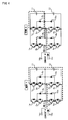
FIG. 5 is a plan view showing an arrangement of the individual semiconductor devices and a flow direction of cooling air on a cooling device of the three-level power converting apparatus according to the first embodiment. Groups of semiconductor devices constituting individually the U-phase unit and the V-phase unit are arranged along the flow direction of the cooling air on aheat sink 15 on a common plane of the cooling device, wherein the semiconductor devices are disposed on the same plane.
As illustrated inFIG. 5 , long sides of the individual switching devices and diodes are oriented in a direction perpendicular to the flow direction of the cooling air with thefirst diodes second diodes heat sink 15. Thefirst switching devices second switching devices first diodes second diodes third switching devices fourth switching devices first diodes second diodes
The cooling air depicted herein is forced cooling air produced by an electric blower (not shown). -
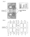
FIG. 6 is an explanatory diagram showing a state of temperature distribution obtained as a result of analysis of temperature increases of the cooling device with an arrangement ofFIG. 5 performed by using general-purpose heat flow analyzing software.FIG. 7 is an explanatory diagram showing a state of temperature distribution obtained in the same way as a result of analysis of temperature increases with the arrangement of the prior art example (Patent Document 1,FIG. 1 ).
To equalize conditions, a radiator portion provided on a rear side of theheat sink 15 of the cooling device employs aluminum fins and a forced cooling air method in which the cooling air is delivered by an electric blower. The aluminum fins of the individual arrangements have the equal fin height, fin length and fin pitch and produce the equal cooling air flow rate, and the heat generation losses occurring in the switching devices are distributed at percentages shown in Table 1. - As shown in
FIG. 6 , the temperature increase of the cooling device reaches a maximum value (Tmax) in an area surrounding thethird switching devices
On the other hand, the temperature increase of the cooling device of the prior art example is large in areas surrounding the second semiconductor device and the third semiconductor device, reaching a maximum value of Tmax=63.4 K (Kelvin) as shown inFIG. 7 .
Thus, it can be recognized from this result that the temperature increases of the cooling device of the three-level power converting apparatus according to this first embodiment are averaged, resulting in a reduction in the maximum value of temperature increase of approximately 10% compared to the prior art example. - In the three-level power converting apparatus according to the first embodiment of the present invention, each phase is made of a single unit and the semiconductor devices of each unit are arranged along the flow direction of the cooling air with the long sides of the individual semiconductor devices oriented at right angles to the flow direction of the cooling air as discussed above. The
first diodes second diodes heat sink 15 with thesecond switching devices third switching devices
Since the semiconductor devices with high heat generation loss are arranged in a distributed fashion, and not adjacent to one another upstream and downstream of the cooling air flow as discussed above, the influence of exhaust heat from the individual switching devices disposed on an upwind side on the switching devices with high heat generation loss disposed on a downwind side is decreased. This makes it possible to average temperature increases of the individual switching devices and thereby increase cooling efficiency of the cooling device. - Also, while the individual switching devices and diodes are arranged as illustrated in
FIG. 5 in the foregoing first embodiment, it is possible to arrange the switching devices and diodes as shown inFIG. 8 . In this modified arrangement, thefirst diodes second diodes first diodes second diodes
Also, an arrangement in which locations of thefirst switching devices second switching devices third switching devices fourth switching devices -
FIG. 9 is a plan view showing an arrangement of individual semiconductor devices and a flow direction of cooling air on a cooling device of a three-level power converting apparatus according to a second embodiment of the present invention. Like the foregoing first embodiment, the second embodiment shows a configuration of the three-level power converting apparatus which is used as a converter having U- and V-phase conversion circuits. Electric circuits and operation of the second embodiment are the same as those of the first embodiment. - As shown in
FIG. 9 , groups of semiconductor devices constituting individually the U-phase unit and the V-phase unit are arranged along the flow direction of the cooling air with long sides of the semiconductor devices oriented in a direction perpendicular to the flow direction of the cooling air. Thefirst switching devices fourth switching devices heat sink 15. Thesecond switching devices first diodes first switching devices fourth switching devices third switching devices second diodes first switching devices fourth switching devices
The cooling air depicted herein is forced cooling air produced by an electric blower (not shown). - In the three-level power converting apparatus according to the second embodiment of the present invention, each phase is made of a single unit and the semiconductor devices of each unit are arranged along the flow direction of the cooling air with the long sides of the individual semiconductor devices oriented at right angles to the flow direction of the cooling air as discussed above. The
first switching devices fourth switching devices heat sink 15 with thesecond switching devices third switching devices
Since the semiconductor devices with high heat generation loss are arranged in a distributed fashion, and not adjacent to one another upstream and downstream of the cooling air flow, the influence of exhaust heat from the individual semiconductor devices disposed on an upwind side on the semiconductor devices with high heat generation loss disposed on a downwind side is decreased. This makes it possible to average temperature increases of the individual semiconductor devices and thereby increase cooling efficiency of the cooling device. - Also, while the individual switching devices and diodes are arranged as depicted in
FIG. 9 in the foregoing second embodiment, an arrangement in which locations of thefirst diodes second switching devices second diodes third switching devices - Furthermore, since the semiconductor devices of the individual units are arranged along the flow direction of the cooling air in the foregoing first and second embodiments, the semiconductor devices have small cross-sectional areas as viewed from surfaces hit by the cooling air and this serves to decrease the air flow rate required for the cooling device to produce. Therefore, it is possible, especially in the case of forced cooling, to decrease the capacity of the electric blower for achieving specific cooling performance.
- While the cooling air is forced cooling air in the foregoing first and second embodiments, the same advantageous effects are obtained with wind hitting a running vehicle.
- Also, a coolant used by the cooling device is the cooling air which is gas in the foregoing first and second embodiments, it is possible to employ a liquid-cooling method in which a liquid, such as cooling water, is used as a coolant which is flowed through a fluid channel provided in close proximity to the individual semiconductor devices. The same advantageous effects are expected to be achieved with this arrangement too.
- As it is possible to make the cooling device more compact by increasing the cooling efficiency of the cooling device, the invention may be used in applications requiring reductions in size and weight.
Claims (2)
- A three-level power converting apparatus in which each of phases constituting a power converting portion is configured by a single unit, each unit comprising:four switching devices including first to fourth switching devices which are connected in series in this order between a positive terminal and a negative terminal of DC side;a first diode connected between a joint between said first switching device and said second switching device and a DC side middle terminal;a second diode connected between a joint between said third switching device and said fourth switching device and said middle terminal; andan AC terminal between said second switching device and said third switching device;wherein said plurality of switching devices and said plurality of diodes constituting each unit are arranged on a heat sink disposed on a common plane of a cooling device and said cooling device is cooled by a coolant flowing in one direction, said three-level power converting apparatus being characterized in that said plurality of diodes are arranged adjacent to one another in a central area of said heat sink, long sides of said individual switching devices are oriented perpendicular to a flow direction of said coolant, said first switching device and said second switching device are arranged on one side of said plurality of diodes whereas said third switching device and said fourth switching device are arranged on the other side of said plurality of diodes, and said plurality of switching devices are arranged along the flow direction of said coolant with said plurality of diodes sandwiched in between.
- A three-level power converting apparatus in which each of phases constituting a power converting portion is configured by a single unit, each unit comprising:four switching devices including first to fourth switching devices which are connected in series in this order between a positive terminal and a negative terminal of DC side;a first diode connected between a joint between said first switching device and said second switching device and a DC side middle terminal;a second diode connected between a joint between said third switching device and said fourth switching device and said middle terminal; andan AC terminal between said second switching device and said third switching device;wherein said plurality of switching devices and said plurality of diodes constituting each unit are arranged on a heat sink disposed on a common plane of a cooling device and said cooling device is cooled by a coolant flowing in one direction, said three-level power converting apparatus being characterized in that long sides of said individual switching devices are oriented perpendicular to a flow direction of said coolant, said first switching device and said fourth switching device are arranged in a central area of said heat sink, said second switching device and said first diode are arranged on one side of said central area whereas said third switching device and said second diode are arranged on the other side of said central area, and said plurality of switching devices and said plurality of diodes are arranged along the flow direction of said coolant.
Applications Claiming Priority (2)
| Application Number | Priority Date | Filing Date | Title |
|---|---|---|---|
| JP2005161661A JP4600159B2 (en) | 2005-06-01 | 2005-06-01 | 3-level power converter |
| PCT/JP2006/307483 WO2006129421A1 (en) | 2005-06-01 | 2006-04-07 | Three level power converter |
Publications (3)
| Publication Number | Publication Date |
|---|---|
| EP1887683A1 true EP1887683A1 (en) | 2008-02-13 |
| EP1887683A4 EP1887683A4 (en) | 2010-12-29 |
| EP1887683B1 EP1887683B1 (en) | 2017-08-02 |
Family
ID=37481354
Family Applications (1)
| Application Number | Title | Priority Date | Filing Date |
|---|---|---|---|
| EP06731430.2A Expired - Lifetime EP1887683B1 (en) | 2005-06-01 | 2006-04-07 | Cooling of a three level power converter |
Country Status (7)
| Country | Link |
|---|---|
| US (1) | US7978488B2 (en) |
| EP (1) | EP1887683B1 (en) |
| JP (1) | JP4600159B2 (en) |
| KR (1) | KR100911067B1 (en) |
| CN (1) | CN100557938C (en) |
| CA (1) | CA2582186C (en) |
| WO (1) | WO2006129421A1 (en) |
Cited By (2)
| Publication number | Priority date | Publication date | Assignee | Title |
|---|---|---|---|---|
| US20130169035A1 (en) * | 2010-09-09 | 2013-07-04 | Mitsubishi Electric Corporation | Power semiconductor module, power conversion apparatus, and railroad vehicle |
| EP2584691A3 (en) * | 2011-10-18 | 2014-07-02 | Hitachi Ltd. | 3-level NPC converter phase module |
Families Citing this family (35)
| Publication number | Priority date | Publication date | Assignee | Title |
|---|---|---|---|---|
| JP4243308B2 (en) | 2007-06-11 | 2009-03-25 | 三菱電機株式会社 | Power converter |
| EP2136465B1 (en) * | 2008-06-18 | 2017-08-09 | SMA Solar Technology AG | Inverter realized by a bridge circuit comprising slow and fast clocked switches |
| JP2011217538A (en) * | 2010-03-31 | 2011-10-27 | Toshiba Corp | Power conversion apparatus |
| WO2011125784A1 (en) * | 2010-03-31 | 2011-10-13 | 株式会社 東芝 | Electric vehicle control device |
| US8929114B2 (en) * | 2011-02-24 | 2015-01-06 | Virginia Tech Intellectual Properties, Inc. | Three-level active neutral point clamped zero voltage switching converter |
| DE102011077160A1 (en) * | 2011-06-07 | 2012-12-13 | Semikron Elektronik Gmbh & Co. Kg | Solar module and method for its operation |
| EP2651025A1 (en) * | 2012-04-10 | 2013-10-16 | ABB Oy | 3-level fullbridge NPC inverter assembly for connection to a single phase grid and photovoltaic power plant comprising the same |
| DE102012206409A1 (en) * | 2012-04-18 | 2013-10-24 | Ge Energy Power Conversion Gmbh | Method for operating an electrical circuit |
| US8619446B2 (en) | 2012-04-27 | 2013-12-31 | Rockwell Automation Technologies, Inc. | Cascaded H-bridge (CHB) inverter level shift PWM with rotation |
| US9425705B2 (en) | 2012-08-13 | 2016-08-23 | Rockwell Automation Technologies, Inc. | Method and apparatus for bypassing cascaded H-bridge (CHB) power cells and power sub cell for multilevel inverter |
| US9007787B2 (en) | 2012-08-13 | 2015-04-14 | Rockwell Automation Technologies, Inc. | Method and apparatus for bypassing Cascaded H-Bridge (CHB) power cells and power sub cell for multilevel inverter |
| JP2014096968A (en) * | 2012-11-12 | 2014-05-22 | Murata Mfg Co Ltd | Inverter device |
| JP2014116995A (en) * | 2012-12-06 | 2014-06-26 | Hitachi Ltd | Three-level power conversion device |
| KR101477359B1 (en) | 2012-12-27 | 2014-12-29 | 삼성전기주식회사 | Power semiconductor module |
| US9240731B2 (en) | 2013-03-18 | 2016-01-19 | Rockwell Automation Technologies, Inc. | Power cell bypass method and apparatus for multilevel inverter |
| US9083230B2 (en) | 2013-06-20 | 2015-07-14 | Rockwell Automation Technologies, Inc. | Multilevel voltage source converters and systems |
| US9520800B2 (en) | 2014-01-09 | 2016-12-13 | Rockwell Automation Technologies, Inc. | Multilevel converter systems and methods with reduced common mode voltage |
| US9325252B2 (en) | 2014-01-13 | 2016-04-26 | Rockwell Automation Technologies, Inc. | Multilevel converter systems and sinusoidal pulse width modulation methods |
| US9559541B2 (en) | 2015-01-15 | 2017-01-31 | Rockwell Automation Technologies, Inc. | Modular multilevel converter and charging circuit therefor |
| JP6429720B2 (en) * | 2015-05-07 | 2018-11-28 | 株式会社日立製作所 | Power converter and railway vehicle |
| JP6429721B2 (en) * | 2015-05-07 | 2018-11-28 | 株式会社日立製作所 | Power converter and railway vehicle |
| US9748862B2 (en) | 2015-05-13 | 2017-08-29 | Rockwell Automation Technologies, Inc. | Sparse matrix multilevel actively clamped power converter |
| CN106891737B (en) * | 2015-12-18 | 2019-03-29 | 比亚迪股份有限公司 | The control method of electric car and its onboard charger and onboard charger |
| JP6735708B2 (en) * | 2016-07-15 | 2020-08-05 | 東芝三菱電機産業システム株式会社 | Cell unit |
| US9812990B1 (en) | 2016-09-26 | 2017-11-07 | Rockwell Automation Technologies, Inc. | Spare on demand power cells for modular multilevel power converter |
| JP6776923B2 (en) * | 2017-02-06 | 2020-10-28 | 株式会社デンソー | Semiconductor device |
| US10097109B1 (en) * | 2017-07-19 | 2018-10-09 | Futurewei Technologies, Inc. | Three-level voltage bus apparatus and method |
| CN108075619A (en) * | 2017-12-25 | 2018-05-25 | 北京天诚同创电气有限公司 | A kind of single-phase power module |
| US10158299B1 (en) | 2018-04-18 | 2018-12-18 | Rockwell Automation Technologies, Inc. | Common voltage reduction for active front end drives |
| EP3690939A1 (en) * | 2019-01-30 | 2020-08-05 | Infineon Technologies AG | Semiconductor arrangements |
| US11211879B2 (en) | 2019-09-23 | 2021-12-28 | Rockwell Automation Technologies, Inc. | Capacitor size reduction and lifetime extension for cascaded H-bridge drives |
| US11690195B2 (en) | 2020-09-11 | 2023-06-27 | Abb Schweiz Ag | Power semiconductor cooling system |
| JP7451386B2 (en) * | 2020-12-08 | 2024-03-18 | 株式会社日立製作所 | power converter |
| US11342878B1 (en) | 2021-04-09 | 2022-05-24 | Rockwell Automation Technologies, Inc. | Regenerative medium voltage drive (Cascaded H Bridge) with reduced number of sensors |
| DE102023132878A1 (en) * | 2023-11-24 | 2025-05-28 | Dr. Ing. H.C. F. Porsche Aktiengesellschaft | Inverter module and inverter |
Family Cites Families (9)
| Publication number | Priority date | Publication date | Assignee | Title |
|---|---|---|---|---|
| EP0838855B1 (en) * | 1991-09-20 | 2004-11-24 | Hitachi, Ltd. | Semiconductor module |
| JP3507911B2 (en) * | 1996-07-19 | 2004-03-15 | 株式会社日立製作所 | Power converter snubber circuit |
| JP3229931B2 (en) * | 1997-09-08 | 2001-11-19 | 三菱電機株式会社 | 3-level power converter |
| JP3652934B2 (en) * | 1999-09-06 | 2005-05-25 | 東芝三菱電機産業システム株式会社 | Power converter |
| EP2234154B1 (en) * | 2000-04-19 | 2016-03-30 | Denso Corporation | Coolant cooled type semiconductor device |
| JP3676268B2 (en) * | 2001-08-01 | 2005-07-27 | 株式会社日立製作所 | Heat transfer structure and semiconductor device |
| KR100767325B1 (en) * | 2001-08-20 | 2007-10-16 | 현대중공업 주식회사 | Power Semiconductor Device Cooling Device for Inverter |
| JP2003079162A (en) * | 2001-09-03 | 2003-03-14 | Toshiba Transport Eng Inc | Power converter |
| US7050311B2 (en) | 2003-11-25 | 2006-05-23 | Electric Power Research Institute, Inc. | Multilevel converter based intelligent universal transformer |
-
2005
- 2005-06-01 JP JP2005161661A patent/JP4600159B2/en not_active Expired - Fee Related
-
2006
- 2006-04-07 KR KR1020077010321A patent/KR100911067B1/en not_active Expired - Fee Related
- 2006-04-07 WO PCT/JP2006/307483 patent/WO2006129421A1/en not_active Ceased
- 2006-04-07 EP EP06731430.2A patent/EP1887683B1/en not_active Expired - Lifetime
- 2006-04-07 CN CNB2006800010844A patent/CN100557938C/en not_active Expired - Fee Related
- 2006-04-07 US US11/663,437 patent/US7978488B2/en not_active Expired - Fee Related
- 2006-04-07 CA CA2582186A patent/CA2582186C/en not_active Expired - Fee Related
Cited By (4)
| Publication number | Priority date | Publication date | Assignee | Title |
|---|---|---|---|---|
| US20130169035A1 (en) * | 2010-09-09 | 2013-07-04 | Mitsubishi Electric Corporation | Power semiconductor module, power conversion apparatus, and railroad vehicle |
| EP2615733A4 (en) * | 2010-09-09 | 2014-04-09 | Mitsubishi Electric Corp | POWER SEMICONDUCTOR MODULE, POWER CONVERTING APPARATUS AND RAILWAY VEHICLE |
| EP2584691A3 (en) * | 2011-10-18 | 2014-07-02 | Hitachi Ltd. | 3-level NPC converter phase module |
| US8922997B2 (en) | 2011-10-18 | 2014-12-30 | Hitachi, Ltd. | Electric power conversion device |
Also Published As
| Publication number | Publication date |
|---|---|
| CA2582186C (en) | 2010-09-21 |
| WO2006129421A1 (en) | 2006-12-07 |
| CA2582186A1 (en) | 2006-12-07 |
| JP4600159B2 (en) | 2010-12-15 |
| US20090207639A1 (en) | 2009-08-20 |
| EP1887683A4 (en) | 2010-12-29 |
| CN100557938C (en) | 2009-11-04 |
| KR20070064658A (en) | 2007-06-21 |
| JP2006340490A (en) | 2006-12-14 |
| US7978488B2 (en) | 2011-07-12 |
| CN101053145A (en) | 2007-10-10 |
| EP1887683B1 (en) | 2017-08-02 |
| KR100911067B1 (en) | 2009-08-06 |
| HK1107729A1 (en) | 2008-04-11 |
Similar Documents
| Publication | Publication Date | Title |
|---|---|---|
| EP1887683B1 (en) | Cooling of a three level power converter | |
| US8300443B2 (en) | Semiconductor module for use in power supply | |
| KR101144409B1 (en) | Power conversion device | |
| US8385068B2 (en) | Cooling of electrical components | |
| CN103312190B (en) | Electric power converter | |
| JP5150570B2 (en) | Three-phase power converter | |
| US8724358B2 (en) | Stacked structure of power conversion apparatus | |
| CN105720834A (en) | Semiconductor device | |
| CN110544685A (en) | power converter | |
| JP7684285B2 (en) | Modular Switching Cell | |
| US20090195066A1 (en) | Power converter | |
| JP2006042406A (en) | Stack structure of power converter | |
| JP2013042663A (en) | Three-phase power conversion apparatus | |
| JP4842018B2 (en) | Power converter | |
| JP2005117783A (en) | Stack structure of power converter | |
| CN212909382U (en) | Three-level current transformation module | |
| US12137543B2 (en) | Power conversion apparatus | |
| JP2000102260A (en) | Power converter | |
| JP2022160942A (en) | Power conversion device | |
| HK1107729B (en) | Three level power converter | |
| Sozinho et al. | Comparison of IGBT modules focus on high power systems | |
| JP2024101333A (en) | Power Conversion Equipment | |
| JP2016171693A (en) | Power converter |
Legal Events
| Date | Code | Title | Description |
|---|---|---|---|
| PUAI | Public reference made under article 153(3) epc to a published international application that has entered the european phase |
Free format text: ORIGINAL CODE: 0009012 |
|
| 17P | Request for examination filed |
Effective date: 20070503 |
|
| AK | Designated contracting states |
Kind code of ref document: A1 Designated state(s): AT BE BG CH CY CZ DE DK EE ES FI FR GB GR HU IE IS IT LI LT LU LV MC NL PL PT RO SE SI SK TR |
|
| DAX | Request for extension of the european patent (deleted) | ||
| A4 | Supplementary search report drawn up and despatched |
Effective date: 20101129 |
|
| 17Q | First examination report despatched |
Effective date: 20151204 |
|
| REG | Reference to a national code |
Ref country code: DE Ref legal event code: R079 Ref document number: 602006053188 Country of ref document: DE Free format text: PREVIOUS MAIN CLASS: H02M0007480000 Ipc: H02M0007483000 |
|
| GRAP | Despatch of communication of intention to grant a patent |
Free format text: ORIGINAL CODE: EPIDOSNIGR1 |
|
| RIC1 | Information provided on ipc code assigned before grant |
Ipc: H02M 7/483 20070101AFI20170123BHEP Ipc: H02M 7/00 20060101ALI20170123BHEP |
|
| INTG | Intention to grant announced |
Effective date: 20170224 |
|
| RIN1 | Information on inventor provided before grant (corrected) |
Inventor name: NAKAGAWA, RYOUSUKE Inventor name: TANAKA, TAKESHI |
|
| GRAS | Grant fee paid |
Free format text: ORIGINAL CODE: EPIDOSNIGR3 |
|
| GRAA | (expected) grant |
Free format text: ORIGINAL CODE: 0009210 |
|
| AK | Designated contracting states |
Kind code of ref document: B1 Designated state(s): AT BE BG CH CY CZ DE DK EE ES FI FR GB GR HU IE IS IT LI LT LU LV MC NL PL PT RO SE SI SK TR |
|
| REG | Reference to a national code |
Ref country code: GB Ref legal event code: FG4D |
|
| REG | Reference to a national code |
Ref country code: CH Ref legal event code: EP Ref country code: AT Ref legal event code: REF Ref document number: 915478 Country of ref document: AT Kind code of ref document: T Effective date: 20170815 |
|
| REG | Reference to a national code |
Ref country code: IE Ref legal event code: FG4D |
|
| REG | Reference to a national code |
Ref country code: DE Ref legal event code: R096 Ref document number: 602006053188 Country of ref document: DE |
|
| REG | Reference to a national code |
Ref country code: NL Ref legal event code: MP Effective date: 20170802 |
|
| REG | Reference to a national code |
Ref country code: AT Ref legal event code: MK05 Ref document number: 915478 Country of ref document: AT Kind code of ref document: T Effective date: 20170802 |
|
| REG | Reference to a national code |
Ref country code: LT Ref legal event code: MG4D |
|
| PG25 | Lapsed in a contracting state [announced via postgrant information from national office to epo] |
Ref country code: NL Free format text: LAPSE BECAUSE OF FAILURE TO SUBMIT A TRANSLATION OF THE DESCRIPTION OR TO PAY THE FEE WITHIN THE PRESCRIBED TIME-LIMIT Effective date: 20170802 Ref country code: FI Free format text: LAPSE BECAUSE OF FAILURE TO SUBMIT A TRANSLATION OF THE DESCRIPTION OR TO PAY THE FEE WITHIN THE PRESCRIBED TIME-LIMIT Effective date: 20170802 Ref country code: LT Free format text: LAPSE BECAUSE OF FAILURE TO SUBMIT A TRANSLATION OF THE DESCRIPTION OR TO PAY THE FEE WITHIN THE PRESCRIBED TIME-LIMIT Effective date: 20170802 Ref country code: AT Free format text: LAPSE BECAUSE OF FAILURE TO SUBMIT A TRANSLATION OF THE DESCRIPTION OR TO PAY THE FEE WITHIN THE PRESCRIBED TIME-LIMIT Effective date: 20170802 Ref country code: SE Free format text: LAPSE BECAUSE OF FAILURE TO SUBMIT A TRANSLATION OF THE DESCRIPTION OR TO PAY THE FEE WITHIN THE PRESCRIBED TIME-LIMIT Effective date: 20170802 |
|
| PG25 | Lapsed in a contracting state [announced via postgrant information from national office to epo] |
Ref country code: GR Free format text: LAPSE BECAUSE OF FAILURE TO SUBMIT A TRANSLATION OF THE DESCRIPTION OR TO PAY THE FEE WITHIN THE PRESCRIBED TIME-LIMIT Effective date: 20171103 Ref country code: PL Free format text: LAPSE BECAUSE OF FAILURE TO SUBMIT A TRANSLATION OF THE DESCRIPTION OR TO PAY THE FEE WITHIN THE PRESCRIBED TIME-LIMIT Effective date: 20170802 Ref country code: ES Free format text: LAPSE BECAUSE OF FAILURE TO SUBMIT A TRANSLATION OF THE DESCRIPTION OR TO PAY THE FEE WITHIN THE PRESCRIBED TIME-LIMIT Effective date: 20170802 Ref country code: IS Free format text: LAPSE BECAUSE OF FAILURE TO SUBMIT A TRANSLATION OF THE DESCRIPTION OR TO PAY THE FEE WITHIN THE PRESCRIBED TIME-LIMIT Effective date: 20171202 Ref country code: BG Free format text: LAPSE BECAUSE OF FAILURE TO SUBMIT A TRANSLATION OF THE DESCRIPTION OR TO PAY THE FEE WITHIN THE PRESCRIBED TIME-LIMIT Effective date: 20171102 Ref country code: LV Free format text: LAPSE BECAUSE OF FAILURE TO SUBMIT A TRANSLATION OF THE DESCRIPTION OR TO PAY THE FEE WITHIN THE PRESCRIBED TIME-LIMIT Effective date: 20170802 |
|
| PG25 | Lapsed in a contracting state [announced via postgrant information from national office to epo] |
Ref country code: CZ Free format text: LAPSE BECAUSE OF FAILURE TO SUBMIT A TRANSLATION OF THE DESCRIPTION OR TO PAY THE FEE WITHIN THE PRESCRIBED TIME-LIMIT Effective date: 20170802 Ref country code: RO Free format text: LAPSE BECAUSE OF FAILURE TO SUBMIT A TRANSLATION OF THE DESCRIPTION OR TO PAY THE FEE WITHIN THE PRESCRIBED TIME-LIMIT Effective date: 20170802 Ref country code: DK Free format text: LAPSE BECAUSE OF FAILURE TO SUBMIT A TRANSLATION OF THE DESCRIPTION OR TO PAY THE FEE WITHIN THE PRESCRIBED TIME-LIMIT Effective date: 20170802 |
|
| REG | Reference to a national code |
Ref country code: DE Ref legal event code: R097 Ref document number: 602006053188 Country of ref document: DE |
|
| PG25 | Lapsed in a contracting state [announced via postgrant information from national office to epo] |
Ref country code: SK Free format text: LAPSE BECAUSE OF FAILURE TO SUBMIT A TRANSLATION OF THE DESCRIPTION OR TO PAY THE FEE WITHIN THE PRESCRIBED TIME-LIMIT Effective date: 20170802 Ref country code: IT Free format text: LAPSE BECAUSE OF FAILURE TO SUBMIT A TRANSLATION OF THE DESCRIPTION OR TO PAY THE FEE WITHIN THE PRESCRIBED TIME-LIMIT Effective date: 20170802 Ref country code: EE Free format text: LAPSE BECAUSE OF FAILURE TO SUBMIT A TRANSLATION OF THE DESCRIPTION OR TO PAY THE FEE WITHIN THE PRESCRIBED TIME-LIMIT Effective date: 20170802 |
|
| PLBE | No opposition filed within time limit |
Free format text: ORIGINAL CODE: 0009261 |
|
| STAA | Information on the status of an ep patent application or granted ep patent |
Free format text: STATUS: NO OPPOSITION FILED WITHIN TIME LIMIT |
|
| 26N | No opposition filed |
Effective date: 20180503 |
|
| PG25 | Lapsed in a contracting state [announced via postgrant information from national office to epo] |
Ref country code: SI Free format text: LAPSE BECAUSE OF FAILURE TO SUBMIT A TRANSLATION OF THE DESCRIPTION OR TO PAY THE FEE WITHIN THE PRESCRIBED TIME-LIMIT Effective date: 20170802 |
|
| PG25 | Lapsed in a contracting state [announced via postgrant information from national office to epo] |
Ref country code: MC Free format text: LAPSE BECAUSE OF FAILURE TO SUBMIT A TRANSLATION OF THE DESCRIPTION OR TO PAY THE FEE WITHIN THE PRESCRIBED TIME-LIMIT Effective date: 20170802 |
|
| REG | Reference to a national code |
Ref country code: CH Ref legal event code: PL |
|
| REG | Reference to a national code |
Ref country code: BE Ref legal event code: MM Effective date: 20180430 |
|
| REG | Reference to a national code |
Ref country code: IE Ref legal event code: MM4A |
|
| PG25 | Lapsed in a contracting state [announced via postgrant information from national office to epo] |
Ref country code: LU Free format text: LAPSE BECAUSE OF NON-PAYMENT OF DUE FEES Effective date: 20180407 |
|
| PG25 | Lapsed in a contracting state [announced via postgrant information from national office to epo] |
Ref country code: CH Free format text: LAPSE BECAUSE OF NON-PAYMENT OF DUE FEES Effective date: 20180430 Ref country code: LI Free format text: LAPSE BECAUSE OF NON-PAYMENT OF DUE FEES Effective date: 20180430 Ref country code: BE Free format text: LAPSE BECAUSE OF NON-PAYMENT OF DUE FEES Effective date: 20180430 |
|
| PG25 | Lapsed in a contracting state [announced via postgrant information from national office to epo] |
Ref country code: FR Free format text: LAPSE BECAUSE OF NON-PAYMENT OF DUE FEES Effective date: 20180430 Ref country code: IE Free format text: LAPSE BECAUSE OF NON-PAYMENT OF DUE FEES Effective date: 20180407 |
|
| PG25 | Lapsed in a contracting state [announced via postgrant information from national office to epo] |
Ref country code: TR Free format text: LAPSE BECAUSE OF FAILURE TO SUBMIT A TRANSLATION OF THE DESCRIPTION OR TO PAY THE FEE WITHIN THE PRESCRIBED TIME-LIMIT Effective date: 20170802 |
|
| PGFP | Annual fee paid to national office [announced via postgrant information from national office to epo] |
Ref country code: GB Payment date: 20200325 Year of fee payment: 15 |
|
| PG25 | Lapsed in a contracting state [announced via postgrant information from national office to epo] |
Ref country code: HU Free format text: LAPSE BECAUSE OF FAILURE TO SUBMIT A TRANSLATION OF THE DESCRIPTION OR TO PAY THE FEE WITHIN THE PRESCRIBED TIME-LIMIT; INVALID AB INITIO Effective date: 20060407 Ref country code: PT Free format text: LAPSE BECAUSE OF FAILURE TO SUBMIT A TRANSLATION OF THE DESCRIPTION OR TO PAY THE FEE WITHIN THE PRESCRIBED TIME-LIMIT Effective date: 20170802 |
|
| PG25 | Lapsed in a contracting state [announced via postgrant information from national office to epo] |
Ref country code: CY Free format text: LAPSE BECAUSE OF FAILURE TO SUBMIT A TRANSLATION OF THE DESCRIPTION OR TO PAY THE FEE WITHIN THE PRESCRIBED TIME-LIMIT Effective date: 20170802 |
|
| REG | Reference to a national code |
Ref country code: DE Ref legal event code: R084 Ref document number: 602006053188 Country of ref document: DE |
|
| GBPC | Gb: european patent ceased through non-payment of renewal fee |
Effective date: 20210407 |
|
| PG25 | Lapsed in a contracting state [announced via postgrant information from national office to epo] |
Ref country code: GB Free format text: LAPSE BECAUSE OF NON-PAYMENT OF DUE FEES Effective date: 20210407 |
|
| PGFP | Annual fee paid to national office [announced via postgrant information from national office to epo] |
Ref country code: DE Payment date: 20220302 Year of fee payment: 17 |
|
| REG | Reference to a national code |
Ref country code: DE Ref legal event code: R119 Ref document number: 602006053188 Country of ref document: DE |
|
| PG25 | Lapsed in a contracting state [announced via postgrant information from national office to epo] |
Ref country code: DE Free format text: LAPSE BECAUSE OF NON-PAYMENT OF DUE FEES Effective date: 20231103 |