JP4842018B2 - Power converter - Google Patents
Power converter Download PDFInfo
- Publication number
- JP4842018B2 JP4842018B2 JP2006151557A JP2006151557A JP4842018B2 JP 4842018 B2 JP4842018 B2 JP 4842018B2 JP 2006151557 A JP2006151557 A JP 2006151557A JP 2006151557 A JP2006151557 A JP 2006151557A JP 4842018 B2 JP4842018 B2 JP 4842018B2
- Authority
- JP
- Japan
- Prior art keywords
- terminals
- conductor plate
- terminal
- power converter
- input
- Prior art date
- Legal status (The legal status is an assumption and is not a legal conclusion. Google has not performed a legal analysis and makes no representation as to the accuracy of the status listed.)
- Expired - Fee Related
Links
Images


Description
本発明は電力変換装置の実装技術に係り、特に電力変換装置の交流入出力端子の接続方法に関する。 The present invention relates to a technology for mounting a power converter, and more particularly to a method for connecting AC input / output terminals of the power converter.
現在、直流と交流の相互の電力変換には半導体スイッチング素子を使った電力変換装置が普及している。電力変換装置では、スイッチング素子のスイッチング時に、回路に存在する寄生インダクタンスにより高いサージ電圧が発生するため、サージ電圧を低減する技術としてスイッチング素子の間やスイッチング素子と電源コンデンサなど間を接続する回路として、導線ではなく導体板が使われている。これによれば、反対方向の電流が流れる導体板同士を近接して配置することで相互インダクタンスにより寄生インダクタンスを低減し、サージ電圧を抑制できる。
このようなサージ電圧を低減する構造は、例えば、特許文献1や特許文献2に開示されている。特許文献1ではP側モジュール4とN側モジュール5との間などを上述の導体板で接続する構造となっており、平滑コンデンサ3とP側モジュール4およびN側モジュール5との間だけではなく、出力端子2への接続も出力端子接続導体14で構成している。
Such a structure for reducing the surge voltage is disclosed in, for example, Patent Document 1 and Patent Document 2. Patent Document 1 has a structure in which the P-side module 4 and the N-side module 5 are connected by the above-described conductor plate, and not only between the smoothing capacitor 3 and the P-side module 4 and the N-side module 5. The connection to the output terminal 2 is also constituted by the output terminal connection conductor 14.
しかしながら上記の従来技術では、複数の端子を持つスイッチング素子を使った場合や、スイッチング素子を複数並列接続した場合には、負荷の接続にも導体板を使っているため、スイッチング素子の特定の端子に電流が集中し、スイッチング素子が破壊してしまうという問題があった。これを、図13を使って説明する。 However, in the above-described prior art, when a switching element having a plurality of terminals is used or when a plurality of switching elements are connected in parallel, a conductor plate is also used for connecting a load. There is a problem that the current is concentrated on the switching element and the switching element is destroyed. This will be described with reference to FIG.
図13は、従来技術を使った2レベルインバータの構造の一部を示しており、特に、上アームIGBTモジュールと下アームIGBTモジュールの接続部だけを示している。101は上アームIGBTモジュール、102は下アームIGBTモジュール、121,122は下アームIGBTモジュールのコレクタ端子、113,114は上アームIGBTモジュールのエミッタ端子、401はエミッタ端子113,114と、コレクタ端子121,122と、電動機への配線とを接続する交流出力導体板、411は交流出力導体板401と電動機への配線とを接続する交流電圧出力端子である。また、421は電流の流れを模式的に示した電流流線であり、本数が電流の大小を示す。
FIG. 13 shows a part of the structure of a two-level inverter using the prior art, and particularly shows only the connection part of the upper arm IGBT module and the lower arm IGBT module. 101 is an upper arm IGBT module, 102 is a lower arm IGBT module, 121 and 122 are collector terminals of the lower arm IGBT module, 113 and 114 are emitter terminals of the upper arm IGBT module, 401 is
電動機から下アームIGBTモジュール102に電流が流れる場合を考えると、交流出力端子411までの経路長が短くなる交流電圧出力端子411に近いコレクタ端子121には電流が多く流れ、遠い端子122に流れる電流は端子121に比べて少なくなる。これは交流出力端子に近い方が抵抗やインダクタンスが小さいためである。
Considering the case where a current flows from the motor to the lower
一般にIGBTモジュールは内部で複数のIGBTチップが並列に接続されている。それぞれの端子には複数のIGBTチップが並列に接続されているため、特定の端子に電流が多く流れると、特定のIGBTチップの電流が多くなる。すると、IGBTモジュールとしては定格電流以下で使っている場合でも、IGBTチップとしては定格以上の電流が流れて、IGBTチップが過電流により破壊する場合があり、問題になっていた。 In general, a plurality of IGBT chips are connected in parallel inside the IGBT module. Since a plurality of IGBT chips are connected in parallel to each terminal, if a large amount of current flows through a specific terminal, the current of the specific IGBT chip increases. Then, even when the IGBT module is used at a rated current or lower, a current exceeding the rated current flows as the IGBT chip, and the IGBT chip may be broken due to an overcurrent, which is a problem.
また、特定のIGBTチップに電流が集中すると、そのチップの発熱が大きくなるために、過電流が流れない場合でも熱破壊する可能性があった。このために現在は大きな冷却器を使うなどして冷却性能を高め、IGBTの熱破壊を防ぐ構成が広く使われているが、装置が大型化し、コストが増大する等の問題が発生していた。 In addition, when current concentrates on a specific IGBT chip, heat generation of the chip increases, so that there is a possibility of thermal destruction even when no overcurrent flows. For this reason, currently, a configuration that increases the cooling performance by using a large cooler and prevents the thermal destruction of the IGBT is widely used, but problems such as an increase in the size of the device and an increase in cost have occurred. .
上記課題を解決するために、本発明の電力変換装置は、直流電圧が印加されている正極端子および負極端子を有するコンデンサと、前記コンデンサの正極端子と第1の導体板を介して接続される第1のスイッチングモジュールと、前記コンデンサの負極端子と第2の導体板を介して接続される第2のスイッチングモジュールと、前記第1のスイッチングモジュールの複数の交流端子と前記第2のスイッチングモジュールの複数の交流端子とを接続する第3の導体板と、を備えた電力変換装置において、前記第3の導体板は、前記第1のスイッチングモジュールの複数の交流端子及び前記第2のスイッチングモジュールの複数の交流端子と接続されており、複数の入出力端子を有し、前記複数の入出力端子から前記第1のスイッチングモジュールの複数の交流端子への経路長は、それぞれ均等であり、前記複数の入出力端子から前記第2のスイッチングモジュールの複数の交流端子への経路長は、それぞれ均等であることとする。
In order to solve the above problems, a power converter of the present invention is connected to a capacitor having a positive electrode terminal and a negative electrode terminal to which a DC voltage is applied, and the positive electrode terminal of the capacitor and a first conductor plate. A first switching module; a second switching module connected via a negative electrode terminal of the capacitor and a second conductor plate; a plurality of AC terminals of the first switching module; and a second switching module. A power converter comprising: a third conductor plate that connects a plurality of AC terminals; and the third conductor plate includes a plurality of AC terminals of the first switching module and a second switching module. The first switching module is connected to a plurality of AC terminals, has a plurality of input / output terminals, and is connected to the first switching module. Path length to a plurality of AC terminals are each equal path lengths to a plurality of AC terminals of the second switching module from the plurality of input and output terminals, and it is respectively equal.
また、直流電圧が印加されている正極端子および負極端子を有するコンデンサと、前記コンデンサの正極端子と第1の導体板を介して接続される複数の第1のスイッチングモジュールと、前記コンデンサの負極端子と第2の導体板を介して接続される複数の第2のスイッチングモジュールと、前記複数の第1のスイッチングモジュールの複数の交流端子と前記複数の第2のスイッチングモジュールの複数の交流端子とを接続する第3の導体板と、を備えた電力変換装置において、前記第3の導体板は、前記複数の第1のスイッチングモジュールの複数の交流端子及び前記複数の第2のスイッチングモジュールの複数の交流端子と接続されており、複数の入出力端子を有し、前記複数の入出力端子から前記複数の第1のスイッチングモジュールの複数の交流端子への経路長は、それぞれ均等であり、前記複数の入出力端子から前記複数の第2のスイッチングモジュールの複数の交流端子への経路長は、それぞれ均等であることでも上記課題を解決できる。
A capacitor having a positive terminal and a negative terminal to which a DC voltage is applied; a plurality of first switching modules connected to the positive terminal of the capacitor via a first conductor plate; and a negative terminal of the capacitor And a plurality of second switching modules connected via the second conductor plate, a plurality of AC terminals of the plurality of first switching modules, and a plurality of AC terminals of the plurality of second switching modules. And a third conductor plate to be connected, wherein the third conductor plate includes a plurality of AC terminals of the plurality of first switching modules and a plurality of the plurality of second switching modules. Connected to an AC terminal, has a plurality of input / output terminals, and the plurality of first switching modules from the plurality of input / output terminals. Path length to a plurality of AC terminals are each equal path lengths to a plurality of AC terminals of said plurality of input and output terminals of the plurality of second switching modules from the also above-mentioned problems that it is equal, respectively can be solved.
本発明によれば、交流電圧出力端子を少なくとも2ヵ所設けることで、交流電圧出力端子からスイッチング素子の端子までの経路長を均一にし、端子の電流を均一にできる。これにより、電流集中によるチップの破壊を防止でき、電力変換装置の信頼性を向上できる。また、特定のチップに電流が集中することによるチップの過剰な温度上昇を防止できるため、冷却装置の小型化、低コスト化が可能である。 According to the present invention, by providing at least two AC voltage output terminals, the path length from the AC voltage output terminal to the terminal of the switching element can be made uniform, and the terminal current can be made uniform. Thereby, destruction of the chip due to current concentration can be prevented, and the reliability of the power conversion device can be improved. In addition, since excessive temperature rise of the chip due to current concentration on a specific chip can be prevented, the cooling device can be reduced in size and cost.
以下に、本発明の実施の形態について、図面を参照して説明する。 Embodiments of the present invention will be described below with reference to the drawings.
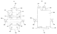
図1〜図4に本発明による実施例1の構造図および回路図を示す。図1(a)は実施例1となる電力変換装置を上面から見た場合のスイッチング素子と、スイッチング素子の上に配置した導体板を示した図、図1(b)は図1(a)の上に配置した導体板を示した図、図2は図1(b)の右側面図、図3は図1および図2の等価回路、図4に交流出力導体板108での電流流線を示している。交流電圧出力端子の位置を説明する便宜上、図1では平滑コンデンサ103と冷却装置109を省略している。また、実施例の説明ではスイッチング素子として、IGBTおよびIGBTと逆並列接続したダイオードを同一パッケージに内蔵したIGBTモジュールを用いる。
1 to 4 show a structure diagram and a circuit diagram of Embodiment 1 according to the present invention. FIG. 1A shows a switching element when the power conversion device according to the first embodiment is viewed from above, and a conductor plate disposed on the switching element, and FIG. 1B shows FIG. FIG. 2 is a right side view of FIG. 1B, FIG. 3 is an equivalent circuit of FIGS. 1 and 2, and FIG. 4 is a current flow line in the AC
2レベル電力変換装置は、正極端子132と負極端子134を持つ直流電源用の平滑コンデンサ103、正極端子132と接続する上アームIGBTモジュール101、負極端子134と接続する下アームIGBTモジュール102、正極端子132とコレクタ端子111、112とを接続する正側導体板104、負極端子134とエミッタ端子123,124と接続する負側導体板106、エミッタ端子113,114とコレクタ端子121,122と接続して、交流電圧を出力する交流出力導体板108、交流出力導体板108と電動機からの配線を接続する交流電圧出力端子135,136、IGBTモジュール101と102での発熱を冷却する冷却装置109で構成される。なお、IGBTモジュールのオン、オフのタイミングを制御するパルス発生装置、およびIGBTのゲート駆動装置は省略している。
The two-level power converter includes a DC power
ここで、電動機から下アームIGBTモジュール102に電流が流れる場合の電流経路を説明する。電流は、交流電圧出力端子135、136から、交流出力導体板108、下アームIGBTモジュール102、負側導体板106を通って、負極端子134に流れる。
Here, a current path when a current flows from the electric motor to the lower
本実施例の特徴は、交流出力導体板108の両端に交流電圧出力端子135,136を設けている点である。これにより、交流電圧出力端子135からコレクタ端子121までの経路長と、交流電圧出力端子136からコレクタ端子122までの経路長が均等になる。
A feature of this embodiment is that AC
このため、交流電圧出力端子135からコレクタ端子121に流れる電流と、交流電圧出力端子136からコレクタ端子122に流れる電流が均一化する。よって、モジュール内のIGBTチップに流れる電流が均一になり、IGBTチップの過電流による破壊を防止できる。
For this reason, the current flowing from the AC
同様に、負極端子134からIGBTと逆並列接続しているダイオードを通って電動機に電流が流れる場合でも、交流出力導体板108の両側に交流電圧出力端子135と136があるため、コレクタ端子121、122から交流電圧出力端子に流れる電流が均一になる。これより、モジュール内のダイオードチップに流れる電流を均一にでき、IGBTモジュール内のダイオードチップが過電流破壊することを防止できる。以上、下アームIGBTモジュール102に電流が流れる場合を説明したが、上アームIGBTモジュール101に電流が流れる場合でも同じ効果が得られる。
Similarly, even when a current flows from the
本実施例では、交流電圧出力端子を2ヵ所設けた場合を示したが、3ヶ所以上設けた場合でも、交流出力端子とIGBTモジュールの端子の経路長をそれぞれ均一にすることで同様の効果を得られる。また、本実施例では、交流電圧出力端子と電動機への配線をボルト等で接続する構造を示しているが、導体板のろう付け等で、交流出力導体板108と電動機の配線を接続した場合でも同様の効果を得られる。
In this embodiment, the case where two AC voltage output terminals are provided is shown, but even when three or more AC terminals are provided, the same effect can be obtained by making the path lengths of the AC output terminal and the IGBT module terminals uniform. can get. Further, in this embodiment, the structure in which the AC voltage output terminal and the wiring to the motor are connected with bolts or the like is shown, but the AC
なお、交流電圧出力端子135と136から電動機の間は、それぞれ配線で接続する、あるいは、電力変換装置内に電動機からの配線を接続する中継端子を設けて、電動機から中継端子までを1本の配線で接続し、中継端子から交流電圧出力端子までをそれぞれ個別の配線で接続する構成が考えられる。
Note that the AC
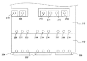
本発明による実施例2として、鉄道等の大容量の電力変換装置で広く使われる3端子対構成のIGBTモジュールを3並列接続した場合を説明する。図5(a)は実施例2となる電力変換装置を上面から見た場合のスイッチング素子の配置図、図5(b)は図5(a)の上に配置した導体板を示した図、図5(c)は図5(b)の上に配置した導体板を示した図、図6は図5(c)の右側面図、図7は交流出力導体板212の電流流線を示している。実施例1の図1と同様に交流電圧出力端子の位置を説明する便宜上、図5では平滑コンデンサ207と冷却装置214を省略している。
As a second embodiment according to the present invention, a description will be given of a case where three IGBT modules having a three-terminal pair configuration widely used in large-capacity power converters such as railways are connected in parallel. FIG. 5A is a layout diagram of switching elements when the power conversion device according to the second embodiment is viewed from above, and FIG. 5B is a diagram illustrating a conductor plate disposed on FIG. 5A. 5C is a diagram showing the conductor plate disposed on FIG. 5B, FIG. 6 is a right side view of FIG. 5C, and FIG. 7 is a current flow line of the AC
本実施例の特徴は、交流出力導体板212と接続する上アームIGBTモジュールのエミッタ端子231〜239を交流電圧出力端子として、電動機への配線を接続する点である。これにより、各交流出力電圧端子と上アームIGBTモジュールのエミッタ端子231〜239の経路長を均等にできる。また、交流電圧出力端子と下アームIGBTモジュールのコレクタ端子241〜249までの経路長も均等にできる。このため、交流電圧出力端子から各IGBTの端子に流れる電流が均一化して、IGBTチップに流れる電流が均一化する。また、実施例1と同様に、コレクタ端子241〜249から交流出力端子に流れる電流も均一になるため、ダイオードチップに流れる電流が均一化する。
The feature of this embodiment is that wiring to the motor is connected using the
なお、図5はエミッタ端子231〜239に導体で構成された端子スペーサ261〜269を接続し、端子スペーサ261〜269と電動機への配線を接続する構成であるが、端子スペーサ261〜269を設けずにIGBTモジュール端子と直接電動機への配線を接続する構成でも同様の効果を得られる。また、図5はエミッタ端子231〜239に電動機への配線を接続した構成であるが、コレクタ端子241〜249を交流電圧出力端子とした構成でも、IGBTチップ、およびダイオードチップに流れる電流を均一にできる。さらに、本実施例では下アームIGBTモジュールに電流が流れた場合について説明したが、上アームIGBTモジュールに電流が流れた場合も同じ効果が得られる。
FIG. 5 shows a configuration in which
本発明による実施例3として、実施例2において交流電圧出力端子から電動機への配線を1枚の導体板で構成した場合を説明する。図8は実施例3となる電力変換装置を上面から見た場合の導体板の構造、図9は図8の右側面図を示している。交流電圧出力端子から電動機への配線となる導体板を説明する便宜上、図8では平滑コンデンサ207と冷却装置214を省略している。
As a third embodiment according to the present invention, a case where the wiring from the AC voltage output terminal to the electric motor in the second embodiment is configured by one conductor plate will be described. 8 shows the structure of the conductor plate when the power conversion device according to the third embodiment is viewed from above, and FIG. 9 shows the right side view of FIG. For the sake of convenience in describing the conductor plate serving as the wiring from the AC voltage output terminal to the motor, the smoothing
本実施例の特徴は、交流電圧出力端子を兼ねる上アームIGBTモジュールのエミッタ端子231〜239から電動機までの配線に導体板213を使用する点である。各々のエミッタ端子231〜239から配線を個別に9本引き出す場合と比較すると、電動機もしくは中継端子での配線の本数を少なくできるため、組立時の取扱性が向上するという効果がある。
The feature of this embodiment is that a
なお、導体板213は配置場所に関わりなく、特定の端子への電流集中の防止効果を得られる。ただし、正側導体板208と負側導体板210の間に導体板213を配置した場合には、導体板213が正側導体板208と負側導体板210の間の磁気結合を遮るため、正側導体板208と負側導体板210の相互インダクタンスによる寄生インダクタンスの低減効果がなくなり、サージ電圧を抑制することが困難になる。よって、図9に示す導体板213と冷却装置214の間に正側導体板208と負側導体板210を配置するか、正側導体板208および負側導体板210と冷却装置214の間に導体板213を配置する構造が望ましい。
In addition, the
また、本実施例で示すように、導体板213を介して交流電圧出力端子と電動機を接続する場合には、導体板213の形状によっては導体板213内を流れる電流の分布に不均一が発生し、エミッタ端子231〜239に流れる電流とコレクタ端子241〜249に流れる電流が不均一になる場合があるために注意を要する。この現象を防止するためには、交流電圧出力端子から中継端子までの経路長を、少なくともエミッタ端子231〜239からコレクタ端子241〜249までの距離よりも長くすることが好ましい。
In addition, as shown in the present embodiment, when the AC voltage output terminal and the motor are connected via the
本発明による実施例4として、3レベル電力変換装置に適用した場合を説明する。図10は3レベル電力変換装置の等価回路図、図11(a)はIGBTモジュール301〜304および結合ダイオードモジュール305,306を直線配置した場合の3レベル電力変換装置の素子配置を上面から見た図、図11(b)は図11(a)の上に配置した導体板を示した図、図11(c)は図11(b)の上に配置した導体板を示した図、図12は図11(c)の電力変換装置を紙面下側から見た図である。
As a fourth embodiment according to the present invention, a case where the present invention is applied to a three-level power conversion device will be described. FIG. 10 is an equivalent circuit diagram of the three-level power converter, and FIG. 11A is a top view of the element arrangement of the three-level power converter when the
本実施例の特徴は3レベル電力変換装置の交流電圧出力端子を2ヵ所設けた点である。この構成によれば、交流電圧出力端子351とコレクタ端子315の経路長と、交流電圧出力端子352とコレクタ端子316の経路長を均等にできるため、IGBTモジュール303のコレクタ端子に流れる電流が均一化する。
The feature of this embodiment is that two AC voltage output terminals of the three-level power converter are provided. According to this configuration, the path length between the AC
また、実施例2と同様に、図11で交流電圧出力端子351と352を設けず、代わりにIGBTモジュール302のエミッタ端子321,322を交流電圧出力端子として、エミッタ端子321,322に電動機への配線を接続することでも、交流電圧出力端子からコレクタ端子315,316に流れる電流が均一化する。なお、コレクタ端子315,316を交流電圧出力端子とした場合でも同様の効果を得られる。
Similarly to the second embodiment, the AC
以上の実施例1〜実施例4では、スイッチング素子としてIGBTモジュールを用いた場合を説明したが、バイポーラトランジスタやMOSFETを用いた場合でも同様の効果を得られる。また、IGBTモジュールのターンオフ時に発生するサージ電圧を抑制するスナバ回路を取り付けていない電力変換装置について説明したが、スナバ回路を取り付けた電力変換装置においても、交流電圧出力端子を少なくとも2ヵ所以上設けることにより特定のIGBTモジュール端子に電流が集中する現象を防止できる。さらに、実施例の図は導体板間の絶縁処理を空間距離にて確保する構造となっているが、導体板の間隔を更に短くして導体板の間に絶縁板を用いて絶縁を確保する方法でも同じ効果を得ることができる。さらに、実施例の説明ではインバータについて説明したが、コンバータに関しても適用することができる。 In the above first to fourth embodiments, the case where the IGBT module is used as the switching element has been described, but the same effect can be obtained even when a bipolar transistor or MOSFET is used. Moreover, although the power converter device which did not attach the snubber circuit which suppresses the surge voltage which generate | occur | produces at the time of turn-off of an IGBT module was demonstrated, also in the power converter device which attached the snubber circuit, provide at least two or more AC voltage output terminals. Therefore, it is possible to prevent a phenomenon in which current concentrates on a specific IGBT module terminal. Further, the drawing of the embodiment has a structure that secures the insulation treatment between the conductor plates at a spatial distance, but it is also possible to further reduce the gap between the conductor plates and secure the insulation by using the insulation plates between the conductor plates. The same effect can be obtained. Furthermore, in the description of the embodiments, the inverter has been described, but the present invention can also be applied to a converter.
本発明は1モジュールで複数の端子対を持つスイッチング素子、およびスイッチング素子を並列接続する電力変換装置に利用できる。特に、鉄道、圧延機、電力分野等の大容量の電力変換装置が必要となる分野において、電流集中を防止することによる冷却装置の小型化、スイッチング素子の長寿命化の効果が大きくなる。 INDUSTRIAL APPLICABILITY The present invention can be used for a switching element having a plurality of terminal pairs in one module and a power conversion device that connects the switching elements in parallel. In particular, in fields where a large-capacity power conversion device is required, such as railways, rolling mills, and the electric power field, the effects of reducing the size of the cooling device and extending the life of the switching element by preventing current concentration are increased.
101 2レベル電力変換装置の上アームIGBTモジュール
102 2レベル電力変換装置の下アームIGBTモジュール
103 平滑コンデンサ
104 正側導体板
106 負側導体板
108 交流出力導体板
109 冷却装置
111,112 IGBTモジュールコレクタ端子
113,114 IGBTモジュールエミッタ端子
121,122 IGBTモジュールコレクタ端子
123.124 IGBTモジュールエミッタ端子
132 正極電源端子
134 負極電源端子
135,136 交流電圧出力端子
141,142 導体板を流れる電流流線
201〜203 2レベル電力変換装置の上アームIGBTモジュール
204〜206 2レベル電力変換装置の下アームIGBTモジュール
207 平滑コンデンサ
208 正側導体板
210 負側導体板
212 交流出力導体板
213 交流出力導体板と同電位で交流電圧出力端子を兼ねるエミッタ端子と接続する導体板
214 冷却装置
221〜229 IGBTモジュールコレクタ端子
231〜239 IGBTモジュールエミッタ端子
241〜249 IGBTモジュールコレクタ端子
251〜259 IGBTモジュールエミッタ端子
261〜269 端子スペーサ
271〜273 正極電源端子
274〜276 負極電源端子
281〜283 導体板を流れる電流流線
291〜299 絶縁確保用の空隙
301〜304 3レベル電力変換装置のIGBTモジュール
305,306 結合ダイオード
307,308 平滑コンデンサ
311〜318 IGBTモジュールコレクタ端子
319〜326 IGBTモジュールエミッタ端子
327〜330 結合ダイオードアノード端子
331〜334 結合ダイオードカソード端子
341 IGBTのエミッタ端子とIGBTのコレクタ端子と結合ダイオードのアノード端子を接続する導体板
342 交流出力導体板
343 IGBTのエミッタ端子とIGBTのコレクタ端子と結合ダイオードのカソード端子を接続する導体板
344 正側導体板
345 中性点接続導体板
346 負側導体板
351,352 交流電圧出力端子
361 正極電源端子
362,363 中性点電源端子
364 負極電源端子
401 交流出力導体板
411 交流電圧出力端子
421 導体板を流れる電流流線
101 Upper-arm IGBT module of 2-level power converter 102 Lower-arm IGBT module of 2-level power converter 103 Smoothing capacitor 104 Positive side conductor plate 106 Negative side conductor plate 108 AC output conductor plate 109 Cooling device 111, 112 IGBT module collector terminal 113, 114 IGBT module emitter terminal 121, 122 IGBT module collector terminal 123.124 IGBT module emitter terminal 132 Positive power supply terminal 134 Negative power supply terminal 135, 136 AC voltage output terminal 141, 142 Current flow lines 201-203 2 flowing through the conductor plate Upper arm IGBT module 204 to 206 of level power converter 204 Lower arm IGBT module of 2-level power converter 207 Smoothing capacitor 208 Positive side conductor plate 210 Negative Conductor plate 212 AC output conductor plate 213 Conductor plate connected to an emitter terminal also serving as an AC voltage output terminal at the same potential as the AC output conductor plate 214 Cooling device 221 to 229 IGBT module collector terminal 231 to 239 IGBT module emitter terminal 241 to 249 IGBT Module collector terminals 251 to 259 IGBT module emitter terminals 261 to 269 Terminal spacers 271 to 273 Positive power source terminals 274 to 276 Negative power source terminals 281 to 283 Current flow lines 291 to 299 flowing through the conductor plates 301 to 304 Three levels IGBT module 305 and 306 of power conversion device Coupling diode 307 and 308 Smoothing capacitor 311 to 318 IGBT module collector terminal 319 to 326 IGBT module emitter terminal 3 27-330 Coupling diode anode terminal 331-334 Coupling diode cathode terminal 341 Conductor plate connecting IGBT emitter terminal, IGBT collector terminal, and anode terminal of coupling diode 342 AC output conductor plate 343 IGBT emitter terminal and IGBT collector terminal 344 Positive side conductive plate 345 Neutral point connection conductive plate 346 Negative side conductive plate 351, 352 AC voltage output terminal 361 Positive power supply terminal 362, 363 Neutral point power supply terminal 364 Negative power supply Terminal 401 AC output conductor plate 411 AC voltage output terminal 421 Current stream line flowing through the conductor plate
Claims (10)
前記コンデンサの正極端子と第1の導体板を介して接続される第1のスイッチングモジュールと、
前記コンデンサの負極端子と第2の導体板を介して接続される第2のスイッチングモジュールと、
前記第1のスイッチングモジュールの複数の交流端子と前記第2のスイッチングモジュールの複数の交流端子とを接続する第3の導体板と、を備えた電力変換装置において、
前記第3の導体板は、前記第1のスイッチングモジュールの複数の交流端子及び前記第2のスイッチングモジュールの複数の交流端子と接続されており、複数の入出力端子を有し、
前記複数の入出力端子から前記第1のスイッチングモジュールの複数の交流端子への経路長は、それぞれ均等であり、
前記複数の入出力端子から前記第2のスイッチングモジュールの複数の交流端子への経路長は、それぞれ均等であることを特徴とする電力変換装置。 A capacitor having a positive terminal and a negative terminal to which a DC voltage is applied;
A first switching module connected to the positive terminal of the capacitor via a first conductor plate;
A second switching module connected to the negative terminal of the capacitor via a second conductor plate;
In a power converter comprising: a third conductor plate that connects a plurality of AC terminals of the first switching module and a plurality of AC terminals of the second switching module ;
The third conductor plate is connected to a plurality of AC terminals of the first switching module and a plurality of AC terminals of the second switching module, and has a plurality of input / output terminals.
Path lengths from the plurality of input / output terminals to the plurality of AC terminals of the first switching module are equal to each other,
The path length from the plurality of input / output terminals to the plurality of AC terminals of the second switching module is equal to each other .
前記コンデンサの正極端子と第1の導体板を介して接続される複数の第1のスイッチングモジュールと、
前記コンデンサの負極端子と第2の導体板を介して接続される複数の第2のスイッチングモジュールと、
前記複数の第1のスイッチングモジュールの複数の交流端子と前記複数の第2のスイッチングモジュールの複数の交流端子とを接続する第3の導体板と、を備えた電力変換装置において、
前記第3の導体板は、前記複数の第1のスイッチングモジュールの複数の交流端子及び前記複数の第2のスイッチングモジュールの複数の交流端子と接続されており、複数の入出力端子を有し、
前記複数の入出力端子から前記複数の第1のスイッチングモジュールの複数の交流端子への経路長は、それぞれ均等であり、
前記複数の入出力端子から前記複数の第2のスイッチングモジュールの複数の交流端子への経路長は、それぞれ均等であることを特徴とする電力変換装置。 A capacitor having a positive terminal and a negative terminal to which a DC voltage is applied;
A plurality of first switching modules connected to the positive terminal of the capacitor via a first conductor plate;
A plurality of second switching modules connected to the negative terminal of the capacitor via a second conductor plate;
In a power converter comprising: a plurality of AC terminals of the plurality of first switching modules; and a third conductor plate that connects the plurality of AC terminals of the plurality of second switching modules .
The third conductor plate is connected to a plurality of AC terminals of the plurality of first switching modules and a plurality of AC terminals of the plurality of second switching modules, and has a plurality of input / output terminals,
The path lengths from the plurality of input / output terminals to the plurality of AC terminals of the plurality of first switching modules are equal, respectively.
The path lengths from the plurality of input / output terminals to the plurality of AC terminals of the plurality of second switching modules are equal to each other .
前記第3の導体板は対向する2辺の対を2組以上有し、一方の対の一方の辺に沿って前記第1のスイッチングモジュールの複数の交流端子が配列され、一方の対の他方の辺に沿って前記第2のスイッチングモジュールの複数の交流端子が接続されており、前記入出力端子が前記他方の対のそれぞれの辺に少なくとも1個づつ設けられていることを特徴とする電力変換装置。 The power conversion device according to claim 1,
The third conductive plate has two or more pairs of two sides facing each other, and a plurality of AC terminals of the first switching module are arranged along one side of one pair, and the other of one pair A plurality of AC terminals of the second switching module are connected along the sides of the second pair, and at least one input / output terminal is provided on each side of the other pair. Conversion device.
前記第1のスイッチングモジュールの少なくとも2個の交流端子が、前記入出力端子を兼ねていることを特徴とする電力変換装置。 In the power converter device according to claim 1 or 2 ,
The power converter according to claim 1, wherein at least two AC terminals of the first switching module also serve as the input / output terminals.
前記第1のスイッチングモジュールの全ての交流端子が、前記入出力端子を兼ねていることを特徴とする電力変換装置。 The power conversion device according to claim 4 ,
All the AC terminals of the first switching module also serve as the input / output terminals.
前記第2のスイッチングモジュールの少なくとも2個の交流端子が、前記入出力端子を兼ねていることを特徴とする電力変換装置。 In the power converter device according to claim 1 or 2 ,
The power converter according to claim 2, wherein at least two AC terminals of the second switching module also serve as the input / output terminals.
前記第2のスイッチングモジュールの全ての交流端子が、前記入出力端子を兼ねていることを特徴とする電力変換装置。 The power conversion device according to claim 6 , wherein
All the AC terminals of the second switching module also serve as the input / output terminals .
前記入出力端子と外部の回路を第4の導体板で接続することを特徴とする電力変換装置。 In the power converter device in any one of Claims 1 thru | or 7 ,
A power converter, wherein the input / output terminal and an external circuit are connected by a fourth conductor plate .
前記第4の導体板が、前記第1の導体板を挟んで、前記第2の導体板と相対する位置にあることを特徴とする電力変換装置。 The power conversion device according to claim 8 , wherein
The power converter according to claim 4, wherein the fourth conductor plate is located at a position facing the second conductor plate with the first conductor plate interposed therebetween.
前記第4の導体板が、前記第2の導体板を挟んで、前記第1の導体板と相対する位置にあることを特徴とする電力変換装置。The power converter according to claim 4, wherein the fourth conductor plate is located at a position facing the first conductor plate with the second conductor plate interposed therebetween.
Priority Applications (1)
| Application Number | Priority Date | Filing Date | Title |
|---|---|---|---|
| JP2006151557A JP4842018B2 (en) | 2006-05-31 | 2006-05-31 | Power converter |
Applications Claiming Priority (1)
| Application Number | Priority Date | Filing Date | Title |
|---|---|---|---|
| JP2006151557A JP4842018B2 (en) | 2006-05-31 | 2006-05-31 | Power converter |
Publications (2)
| Publication Number | Publication Date |
|---|---|
| JP2007325387A JP2007325387A (en) | 2007-12-13 |
| JP4842018B2 true JP4842018B2 (en) | 2011-12-21 |
Family
ID=38857692
Family Applications (1)
| Application Number | Title | Priority Date | Filing Date |
|---|---|---|---|
| JP2006151557A Expired - Fee Related JP4842018B2 (en) | 2006-05-31 | 2006-05-31 | Power converter |
Country Status (1)
| Country | Link |
|---|---|
| JP (1) | JP4842018B2 (en) |
Families Citing this family (5)
| Publication number | Priority date | Publication date | Assignee | Title |
|---|---|---|---|---|
| JP2012165621A (en) * | 2011-02-09 | 2012-08-30 | Toshiba Corp | Power converter |
| JP6493171B2 (en) * | 2015-11-18 | 2019-04-03 | 株式会社デンソー | Power converter |
| JP6293941B2 (en) * | 2017-02-21 | 2018-03-14 | 株式会社日立製作所 | 3-level power converter |
| JP7283143B2 (en) | 2019-03-12 | 2023-05-30 | 富士電機株式会社 | power converter |
| CN111986609B (en) * | 2020-08-31 | 2021-11-23 | 武汉华星光电技术有限公司 | Gate drive circuit and display device |
Family Cites Families (5)
| Publication number | Priority date | Publication date | Assignee | Title |
|---|---|---|---|---|
| JPS63164386A (en) * | 1986-12-26 | 1988-07-07 | Matsushita Electric Ind Co Ltd | Semiconductor laser |
| JPH06261556A (en) * | 1993-03-04 | 1994-09-16 | Toshiba Corp | Semiconductor switch apparatus |
| JP3247197B2 (en) * | 1993-05-13 | 2002-01-15 | 株式会社東芝 | Semiconductor power converter |
| JPH06351262A (en) * | 1993-06-04 | 1994-12-22 | Toshiba Corp | Semiconductor switching device |
| JP2001086770A (en) * | 1999-09-13 | 2001-03-30 | Hitachi Ltd | Main circuit structure of power converter |
-
2006
- 2006-05-31 JP JP2006151557A patent/JP4842018B2/en not_active Expired - Fee Related
Also Published As
| Publication number | Publication date |
|---|---|
| JP2007325387A (en) | 2007-12-13 |
Similar Documents
| Publication | Publication Date | Title |
|---|---|---|
| US10153708B2 (en) | Three-level power converter | |
| JP4920677B2 (en) | Power conversion device and assembly method thereof | |
| JP5132175B2 (en) | Power converter | |
| EP2884650B1 (en) | Power module comprising two elements, and three-level power conversion device using same | |
| US10134718B2 (en) | Power semiconductor module | |
| JP2004214452A (en) | Semiconductor module for power and method for connecting to external electrode | |
| JP6196853B2 (en) | 3 level converter half bridge | |
| JP2014033060A (en) | Power semiconductor device module | |
| JP2014036509A (en) | Three-level power conversion device | |
| JP2014217270A (en) | Half bridge for 3-level power conversion device | |
| JP2020017623A (en) | Semiconductor device | |
| JP4842018B2 (en) | Power converter | |
| US20090195066A1 (en) | Power converter | |
| JP2012105382A (en) | Semiconductor device | |
| JP4455914B2 (en) | Power converter | |
| US10554123B2 (en) | Power converter with a parallel flat plate conductor electrically connected with a capacitor and a power module | |
| WO2019146179A1 (en) | Power conversion device and electric railroad vehicle equipped with power conversion device | |
| JP2006158107A (en) | 3-level inverter device | |
| JP6575072B2 (en) | Phase unit and three-level power converter using the same | |
| JP4827174B2 (en) | Boost chopper device | |
| JP2017169344A (en) | Power conversion device | |
| JP2021184406A (en) | Semiconductor module for electric power | |
| JP2006271131A (en) | Power converter | |
| JP6134798B2 (en) | Power converter | |
| JP6493171B2 (en) | Power converter |
Legal Events
| Date | Code | Title | Description |
|---|---|---|---|
| A621 | Written request for application examination |
Free format text: JAPANESE INTERMEDIATE CODE: A621 Effective date: 20080526 |
|
| A977 | Report on retrieval |
Free format text: JAPANESE INTERMEDIATE CODE: A971007 Effective date: 20110214 |
|
| A131 | Notification of reasons for refusal |
Free format text: JAPANESE INTERMEDIATE CODE: A131 Effective date: 20110222 |
|
| A521 | Written amendment |
Free format text: JAPANESE INTERMEDIATE CODE: A523 Effective date: 20110711 |
|
| TRDD | Decision of grant or rejection written | ||
| A01 | Written decision to grant a patent or to grant a registration (utility model) |
Free format text: JAPANESE INTERMEDIATE CODE: A01 Effective date: 20111004 |
|
| A01 | Written decision to grant a patent or to grant a registration (utility model) |
Free format text: JAPANESE INTERMEDIATE CODE: A01 |
|
| A61 | First payment of annual fees (during grant procedure) |
Free format text: JAPANESE INTERMEDIATE CODE: A61 Effective date: 20111005 |
|
| R150 | Certificate of patent (=grant) or registration of utility model |
Free format text: JAPANESE INTERMEDIATE CODE: R150 |
|
| FPAY | Renewal fee payment (prs date is renewal date of database) |
Free format text: PAYMENT UNTIL: 20141014 Year of fee payment: 3 |
|
| LAPS | Cancellation because of no payment of annual fees |