EP1887637A2 - Light emitting device package and method for manufacturing the same - Google Patents
Light emitting device package and method for manufacturing the same Download PDFInfo
- Publication number
- EP1887637A2 EP1887637A2 EP07253107A EP07253107A EP1887637A2 EP 1887637 A2 EP1887637 A2 EP 1887637A2 EP 07253107 A EP07253107 A EP 07253107A EP 07253107 A EP07253107 A EP 07253107A EP 1887637 A2 EP1887637 A2 EP 1887637A2
- Authority
- EP
- European Patent Office
- Prior art keywords
- light emitting
- emitting device
- substrate
- package
- over
- Prior art date
- Legal status (The legal status is an assumption and is not a legal conclusion. Google has not performed a legal analysis and makes no representation as to the accuracy of the status listed.)
- Granted
Links
Images





Classifications
-
- H—ELECTRICITY
- H10—SEMICONDUCTOR DEVICES; ELECTRIC SOLID-STATE DEVICES NOT OTHERWISE PROVIDED FOR
- H10H—INORGANIC LIGHT-EMITTING SEMICONDUCTOR DEVICES HAVING POTENTIAL BARRIERS
- H10H20/00—Individual inorganic light-emitting semiconductor devices having potential barriers, e.g. light-emitting diodes [LED]
- H10H20/80—Constructional details
- H10H20/85—Packages
- H10H20/851—Wavelength conversion means
- H10H20/8514—Wavelength conversion means characterised by their shape, e.g. plate or foil
-
- H—ELECTRICITY
- H10—SEMICONDUCTOR DEVICES; ELECTRIC SOLID-STATE DEVICES NOT OTHERWISE PROVIDED FOR
- H10H—INORGANIC LIGHT-EMITTING SEMICONDUCTOR DEVICES HAVING POTENTIAL BARRIERS
- H10H20/00—Individual inorganic light-emitting semiconductor devices having potential barriers, e.g. light-emitting diodes [LED]
- H10H20/80—Constructional details
- H10H20/85—Packages
- H10H20/8506—Containers
-
- H—ELECTRICITY
- H10—SEMICONDUCTOR DEVICES; ELECTRIC SOLID-STATE DEVICES NOT OTHERWISE PROVIDED FOR
- H10W—GENERIC PACKAGES, INTERCONNECTIONS, CONNECTORS OR OTHER CONSTRUCTIONAL DETAILS OF DEVICES COVERED BY CLASS H10
- H10W72/00—Interconnections or connectors in packages
- H10W72/01—Manufacture or treatment
- H10W72/0198—Manufacture or treatment batch processes
-
- H—ELECTRICITY
- H10—SEMICONDUCTOR DEVICES; ELECTRIC SOLID-STATE DEVICES NOT OTHERWISE PROVIDED FOR
- H10W—GENERIC PACKAGES, INTERCONNECTIONS, CONNECTORS OR OTHER CONSTRUCTIONAL DETAILS OF DEVICES COVERED BY CLASS H10
- H10W72/00—Interconnections or connectors in packages
- H10W72/851—Dispositions of multiple connectors or interconnections
- H10W72/874—On different surfaces
- H10W72/884—Die-attach connectors and bond wires
-
- H—ELECTRICITY
- H10—SEMICONDUCTOR DEVICES; ELECTRIC SOLID-STATE DEVICES NOT OTHERWISE PROVIDED FOR
- H10W—GENERIC PACKAGES, INTERCONNECTIONS, CONNECTORS OR OTHER CONSTRUCTIONAL DETAILS OF DEVICES COVERED BY CLASS H10
- H10W90/00—Package configurations
- H10W90/701—Package configurations characterised by the relative positions of pads or connectors relative to package parts
- H10W90/721—Package configurations characterised by the relative positions of pads or connectors relative to package parts of bump connectors
- H10W90/724—Package configurations characterised by the relative positions of pads or connectors relative to package parts of bump connectors between a chip and a stacked insulating package substrate, interposer or RDL
-
- H—ELECTRICITY
- H10—SEMICONDUCTOR DEVICES; ELECTRIC SOLID-STATE DEVICES NOT OTHERWISE PROVIDED FOR
- H10W—GENERIC PACKAGES, INTERCONNECTIONS, CONNECTORS OR OTHER CONSTRUCTIONAL DETAILS OF DEVICES COVERED BY CLASS H10
- H10W90/00—Package configurations
- H10W90/701—Package configurations characterised by the relative positions of pads or connectors relative to package parts
- H10W90/731—Package configurations characterised by the relative positions of pads or connectors relative to package parts of die-attach connectors
- H10W90/736—Package configurations characterised by the relative positions of pads or connectors relative to package parts of die-attach connectors between a chip and a stacked lead frame, conducting package substrate or heat sink
-
- H—ELECTRICITY
- H10—SEMICONDUCTOR DEVICES; ELECTRIC SOLID-STATE DEVICES NOT OTHERWISE PROVIDED FOR
- H10W—GENERIC PACKAGES, INTERCONNECTIONS, CONNECTORS OR OTHER CONSTRUCTIONAL DETAILS OF DEVICES COVERED BY CLASS H10
- H10W90/00—Package configurations
- H10W90/701—Package configurations characterised by the relative positions of pads or connectors relative to package parts
- H10W90/751—Package configurations characterised by the relative positions of pads or connectors relative to package parts of bond wires
- H10W90/753—Package configurations characterised by the relative positions of pads or connectors relative to package parts of bond wires between laterally-adjacent chips
-
- H—ELECTRICITY
- H10—SEMICONDUCTOR DEVICES; ELECTRIC SOLID-STATE DEVICES NOT OTHERWISE PROVIDED FOR
- H10W—GENERIC PACKAGES, INTERCONNECTIONS, CONNECTORS OR OTHER CONSTRUCTIONAL DETAILS OF DEVICES COVERED BY CLASS H10
- H10W90/00—Package configurations
- H10W90/701—Package configurations characterised by the relative positions of pads or connectors relative to package parts
- H10W90/751—Package configurations characterised by the relative positions of pads or connectors relative to package parts of bond wires
- H10W90/756—Package configurations characterised by the relative positions of pads or connectors relative to package parts of bond wires between a chip and a stacked lead frame, conducting package substrate or heat sink
Definitions
- the present invention relates to a light emitting device package and a method for manufacturing the same, and more particularly, to a light emitting device package capable of emitting uniform white light and a method for manufacturing the same.
- LEDs Light emitting diodes
- GaAsP compound semiconductors Since a red LED using GaAsP compound semiconductors was made commercially available in 1962, it has been used, together with a GaP:N-based green LED, as a light source in electronic apparatuses, for image display.
- the wavelength of light emitted from such an LED depends on the semiconductor material used to fabricate the LED. This is because the wavelength of the emitted light depends on the band-gap of the semiconductor material representing energy difference between valence-band electrons and conduction-band electrons.
- GaN gallium nitride
- LEDs light emitting diodes
- GaN compound semiconductor has been highlighted in the field of high-power electronic devices including light emitting diodes (LEDs) because it exhibits a high thermal stability and a wide band-gap of 0.8 to 6.2eV.
- LEDs light emitting diodes
- One of the reasons why the GaN compound semiconductor has been highlighted is that it is possible to fabricate semiconductor layers capable of emitting green, blue, and white light, using GaN in combination with other elements, for example, indium (In), aluminum (Al), etc.
- Such a white light source may be fabricated using LEDs for emitting light of three primary colors, namely, red, green, and blue, or using an LED for emitting light of a certain color and phosphors.
- a white light source may be fabricated using a blue LED and yellow phosphors.
- white light is produced as blue light emitted from a blue LED and yellow light emitted from yellow phosphors excited by the blue light are mixed.
- the white light source may be fabricated using a green LED and red phosphors or using an ultraviolet LED and red, green, and blue phosphors.
- red light and green light are emitted as blue light emitted from the blue LED is absorbed in the yellow phosphors in certain degrees.
- the red light and green light are mixed with the blue light not absorbed in the yellow phosphors, so that they are viewed in the form of white light to the observer.
- the above-mentioned method which uses a blue LED and yellow phosphors, to fabricate a white light source, are widely used because the fabricated white light source exhibits excellent color rendering, high stability, and high reliability.
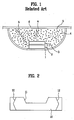
- FIG. 1 illustrates an LED lamp which emits white light using the above-mentioned LED and phosphors.
- a blue LED 3 is disposed on a stack 2 mounted in a reflective cup 1.
- a glass 6 is arranged over the filler 5.
- the filler 5 enclosing the LED 3 may have a non-uniform thickness. For this reason, there may be an optical path length difference between light paths a and b of light emitted from the LED 3 to the surface of the glass 6.
- the present invention is directed to a light emitting device package and a method for manufacturing the same.
- Embodiments of the present invention can provide a light emitting device package capable of emitting light generated from a light source via an external medium while achieving a reduction in optical path length difference, thereby achieving an improvement in the chromatic uniformity at different positions of the light emitting device, and enabling emission of light uniformly changed in wavelength.
- a first aspect of the invention provides a light emitting device package comprises: a package body; an electrode formed over at least one surface of the package body; a light emitting device mounted over the package body; and a phosphor layer formed over the light emitting device while having a uniform thickness around the light emitting device.
- FIG. 1 is a schematic view illustrating a general light emitting device package
- FIGs. 2 to 8 are views illustrating a first embodiment of the present invention
- FIGs. 9 to 13 are views illustrating a second embodiment of the present invention.
- FIGs. 14 to 18 are views illustrating a third embodiment of the present invention.
- FIG. 19 is a view illustrating a fourth embodiment of the present invention.
- FIGs. 20 to 22 are views illustrating a fifth embodiment of the present invention.
- FIGs. 23 to 25 are views illustrating a sixth embodiment of the present invention.
- FIGs. 26 is a view illustrating a seventh embodiment of the present invention.
- FIGs . 27 and 28 are views illustrating an eighth embodiment of the present invention.
- FIGs. 29 to 33 are views illustrating a ninth embodiment of the present invention.
- FIGs. 34 to 38 are views illustrating a tenth embodiment of the present invention.
- first region, layer or section discussed below could be termed a second region, layer or section, and similarly, a second region, layer or section may be termed a first region, layer or section without departing from the teachings of the present invention.
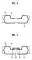
- a substrate 10 which is provided with a groove-shaped mount 11 formed at an upper surface of the substrate 10, and side grooves 12 formed at opposite side surfaces of the substrate 10, is prepared, as shown in FIG. 2.
- the structure of the substrate 10 is also illustrated in FIG. 7.
- a silicon substrate or a ceramic substrate may be used.
- the side grooves 12 may be formed by forming through holes at opposite sides of the substrate 10.
- each electrode 13 connects the interior of the mount 11, an associated one of the side grooves 12, and a lower surface of the substrate 10, as shown in FIG. 3.
- a light emitting device 20 is then bonded on the substrate 10 inside the mount 11 such that the light emitting device 20 is connected to the electrodes 13, as shown in FIG. 4.
- the bonding of the light emitting device 20 may be achieved using solders 21 applied to respective terminals of the electrodes 13 of the light emitting device 20.
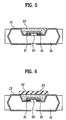
- a filler 22 is filled in the interior of the mount 11 such that the filler 22 encloses the light emitting device 20, as shown in FIG. 5.
- a transparent material which allows light to pass therethrough, may be used.
- a silicon gel or an epoxy resin may be used.
- the resin layer 23 may have a uniform thickness. Thus, a light emitting device package is completely manufactured.
- the wavelength-changed light is emitted from the light emitting device package.
- the light emitting device 20 is a blue light emitting device
- the phosphors dispersed in the resin layer 23 are yellow phosphors
- blue light generated from the blue light emitting device 20 is mixed with yellow light generated from the yellow phosphors while passing through the resin layer 23.
- white light may be emitted from the light emitting device package.
- the mount 11 is formed at the upper surface of the substrate 10. Also, the side grooves 12 are formed at opposite sides of the mount 11.
- each side surface of the substrate 10 has a centrally-protruded shape by inclinedly etching upper and lower portions of the side surface upon forming the associated side groove 12.
- the mount 11 also has inclined side walls, so that light emitted from the light emitting device 10 mounted on the bottom surface of the mount 11 can be reflected from the inclined side walls. In this case, it is possible to increase the amount of light output through the top of the package.
- FIG. 8 illustrates optical travel paths in the light emitting device package according to this embodiment. As shown in FIG. 8, light emerging from the top of the light emitting device 20 mounted on the bottom surface of the mount 11 travels along an optical path B, whereas light emerging from each side surface of the light emitting device 20 travels along an optical path A after being reflected by the side surface of the mount 11 facing the side surface of the light emitting device 20.
- the light traveling along the optical path A and the light traveling along the optical path B passes through the phosphor-distributed resin layer 23, which has a uniform thickness, so that the wavelength of the light is uniformly changed.
- a mounting recess 31 is first formed at an upper surface of a substrate 30.
- a pair of electrodes 32 are then formed in the mounting recess 31 such that the electrodes 32 extend along side walls of the mounting recess 31 and then extend along the upper surface of the substrate 30.
- a light emitting device 40 is then bonded on the substrate to portions of the electrodes 32 arranged in the mounting recess 31, as shown in FIG. 10. Subsequently, a filler 42 is filled in the mounting recess 31. A phosphor-distributed resin layer 43 is the formed over the mounting recess 31 filled with the filler 42.
- the bonding of the light emitting device 40 may be achieved by bonding terminals of the light emitting device 40 to the electrodes 32 using solders 41, as in the first embodiment as described above.
- the filling of the filler 42 may be achieved using a dispensing method, as shown in FIG. 11.
- a nozzle 82 which contains the filler 42, is positioned in the mounting recess 31 above the light emitting device 40.
- the filler 42 is then discharged from the nozzle 82, to fill the mounting recess 31.
- the formation of the resin layer 43 over the filler 42 may be achieved using a screen printing process, as shown in FIG. 12.
- a stencil 80 having an opening is first prepared.
- the stencil 80 is then arranged on the filler 42 such that the filler 42 is exposed through the opening of the stencil 80.
- a phosphor-distributed resin material is supplied to the opening of the stencil 80 such that the resin material is applied to the filler 42.
- the resin material is then spread using a squeegee 81 arranged over the stencil 80 such that the resin material forms a film.
- the phosphor-distributed resin layer 43 on the filler 42 in the form of a film having a uniform thickness.
- the resin layer 43 may be formed by separately preparing a phosphor-distributed resin film, and attaching the resin film to an upper surface of the filler 42, as shown in FIG. 13.
- the remaining configurations of the second embodiment may be identical to those of the first embodiment, and so, no description thereof will be given.
- a pair of electrodes 51 are formed at opposite sides of a first substrate 50 such that the upper and lower surfaces of the first substrate 50 are connected by each electrode 51.
- a second substrate 52 which includes a mounting hole 53, as shown in FIG. 15, is prepared.
- a reflective film is formed on the mounting hole 53 of the second substrate 52.
- the reflective film functions to reflect light emerging from a light emitting device, which will be mounted in a subsequent process, and thus to increase the amount of light emitted through the top of the package.
- the second substrate 52 is attached to the first substrate 50 such that the electrodes 51 are partially exposed through the mounting hole 53.
- the substrate attachment may be achieved using an adhesive 54 such as an adhesive resin or an adhesive tape.
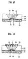
- a light emitting device 60 is bonded to the electrodes 51 exposed through the mounting hole 53 of the second substrate 52, as shown in FIG. 17.
- a filler 62 is then filled in the mounting hole 53.
- a phosphor-distributed resin layer 63 is formed over the filler 62, as shown in FIG. 18.
- a silicon substrate or a ceramic substrate may be used for each of the first and second substrates 50 and 52.
- a ceramic substrate it is preferred that the substrate is made of a material exhibiting excellent heat conductivity.
- the substrates may also be made of a material exhibiting excellent thermal insulation, for example, AlN or alumina.
- FIG. 19 illustrates a light emitting device package according to a fourth embodiment of the present invention.
- FIG. 19 shows a state in which a zener diode 73 is mounted together with a light emitting device 72, to achieve an improvement in voltage withstand characteristics.
- the light emitting device 72 and zener diode 73 are bonded using wires in a state in which a pair of leads 70 and 71 are formed in a package body.
- a filler 75 is formed over the light emitting device 72 and zener diode 73.
- a phosphor-distributed resin layer 76 is also formed over the filler 75.
- a package is configured by connecting the zener diode 73 and light emitting device 72 in parallel, as described above, over-current generated when a surge voltage is applied to the light emitting device 72, which exhibits inferior voltage withstand characteristics, namely, inferior resistance to static electricity, does not flow toward the light emitting device 72. That is, a zener breakdown occurs in the zener diode 73 near a zener voltage due to the over-current, thereby causing the over-current to be bypassed through the zener diode 73. Thus, the light emitting device 72 is protected from the over-current.
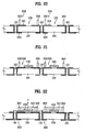
- FIGs. 20 to 22 illustrate procedures for manufacturing a light emitting device package according to a fifth embodiment of the present invention.
- through holes 110 are first formed through a substrate 100 using a laser or an etching method, as shown in FIG. 20.
- the substrate 100 may be one of a ceramic substrate or a silicon substrate to be used for a 2D sub-mount or a package for a light emitting device.
- the substrate 100 which is formed with the through holes 110, as described above, forms a package body.
- electrodes 200 to be connected to mounts 120, on which light emitting devices will be mounted are formed on the surface of the substrate 100.
- Each electrode 200 has a structure connected between the front and back surfaces of the substrate 100 using a metal line. That is, each electrode 200 includes a front-side electrode 210 connected to a light emitting device, and a back-side electrode 220 formed at the back surface of the substrate 100 and connected to the front-side electrode 210 via one through hole 110.
- the back-side electrode 220 may be electrically connected to an external circuit functioning to supply current to a light emitting device.
- the through holes 110 be formed in an isolation region of the package.
- Uniformly-spaced barrier ribs 300 exhibiting excellent light transmissivity are formed at the front surface of the substrate 100, on which light emitting devices 400 will be mounted.
- the barrier ribs 300 may be made of a photosensitive polymer. That is, the formation of the barrier ribs 300 can be achieved by coating a photosensitive polymer over the front surface of the substrate 100, and performing a photolithography process such that the photosensitive polymer remains in a region where the barrier ribs 300 will be formed, while being removed in other regions.
- the barrier ribs 300 may be formed by separately fabricating barrier ribs using a material exhibiting excellent light transmissivity, for example, glass, and bonding the fabricated barrier ribs to the substrate 100.
- the light emitting devices 400 are bonded to the sub-mount or package, as shown in FIG. 21.
- a filler 310 such as a phosphor-containing epoxy resin or silicon gel, is then filled in spaces between the barrier ribs 300 and the light emitting devices 400, as shown in FIG. 22.
- each barrier rib 300 and the upper surface of each light emitting device 400 be equal to the distance between the barrier rib 300 and the side surface of the light emitting device 400 facing the barrier rib 300.
- each light emitting device 400 any of a horizontal type light emitting device and a vertical type light emitting device can be used.
- lenses may be mounted to the substrate 100 packaged with the light emitting devices 400.
- the substrate 100 is then divided into individual packages.
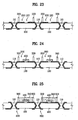
- FIGs. 23 to 25 illustrate procedures for manufacturing a light emitting device package according to a sixth embodiment of the present invention.
- through holes 110 are first formed through a silicon substrate 100 using a solution enabling anisotropic etching, for example, a KOH or tetramethyl ammonium hydroxide (TMAH) solution, as shown in FIG. 23.
- a solution enabling anisotropic etching for example, a KOH or tetramethyl ammonium hydroxide (TMAH) solution, as shown in FIG. 23.
- the substrate 100 may be used for a sub-mount or a package for a light emitting device.
- the through holes 110 are formed in accordance with an etching process, as described above, they have a structure as shown in FIG. 23.
- the etching for the formation of the through holes 110 is carried out at both the front and back surfaces of the substrate 100 such that the etched front and back portions of the substrate 100 to form each through hole 110 are connected.
- electrodes 200 to be connected to mounts 120, on which light emitting devices will be mounted are formed on the surface of the substrate 100.
- each electrode 200 may include a front-side electrode 210 connected to a light emitting device, and a back-side electrode 220 formed at the back surface of the substrate 100 and connected to the front-side electrode 210 via one through hole 110.
- barrier ribs 300 are formed, and light emitting devices 400 are mounted to the mounts 120, as shown in FIG. 24.
- a filler 310 is then filled in spaces defined by the barrier ribs 300 inside the barrier ribs 300, as shown in FIG. 25. Subsequent procedures are identical to those of the fifth embodiment.
- FIG. 26 illustrates a light emitting device package according to a seventh embodiment of the present invention.
- a light emitting device 400 is bonded to an aluminum slug 130 having a mirror surface, using an adhesive 140.
- a barrier rib 300 is formed around the light emitting device 400, using a material exhibiting excellent light transmissivity.
- a filler 310 such as a phosphor-containing epoxy resin or silicon gel, is filled between the barrier rib 300 and the light emitting device 400.
- the electrodes of the light emitting device 400 is electrically connected to leads 150 fixed to a package body 101, using conductive wires 160.
- a lens 170 is formed on or directly attached to an upper surface of the package body 101, on which the light emitting device 400 is mounted.
- the height difference between the barrier rib 300 and the upper surface of the light emitting device 400 be equal to the distance between the barrier rib 300 and the side surface of the light emitting device 400 facing the barrier rib 300.
- FIGs. 27 and 28 illustrate procedures for manufacturing a light emitting device package according to an eighth embodiment of the present invention.
- through holes 110 are first formed through a substrate 100 using a laser or an etching method, as shown in FIG. 27.
- the substrate 100 may be one of a ceramic substrate or a silicon substrate to be used for a sub-mount or a package for a light emitting device.
- Mounts 120, on which light emitting devices will be mounted, are also formed at the substrate 100
- each mount 120 has a recess structure formed as the substrate 100 is recessed in accordance with an etching process. By virtue of such a structure, each mount 120 can upwardly reflect light emitted from each side surface of the light emitting device.
- the substrate 100 which is formed with the through holes 110, as described above, forms a package body.
- electrodes 200 are formed on the substrate 100 such that each electrode 200 has a structure connected between the front and back surfaces of the substrate 100 using a metal line.
- the through holes 110 be formed in an isolation region of the package.
- Uniformly-spaced barrier ribs 300 exhibiting excellent light transmissivity are formed at the front surface of the substrate 100, on which light emitting devices 400 will be mounted.
- the barrier ribs 300 may be made of a photosensitive polymer. That is, the formation of the barrier ribs 300 can be achieved by coating a photosensitive polymer over the front surface of the substrate 100, and performing a photolithography process such that the photosensitive polymer remains in a region where the barrier ribs 300 will be formed, while being removed in other regions.
- the barrier ribs 300 may be formed by separately fabricating barrier ribs using a material exhibiting excellent light transmissivity, for example, glass, and bonding the fabricated barrier ribs to the substrate 100.
- the light emitting devices 400 are mounted to the sub-mount or package in accordance with, for example, a flip chip bonding process.
- each light emitting device 400 may be bonded to the associated electrode 200 in a state in which the light emitting device 400 has a structure inverted from a horizontal structure.
- a zener diode (not shown) may be provided at the electrode 200.
- a filler 310 such as a phosphor-containing epoxy resin or silicon gel, is filled in spaces between the barrier ribs 300 and the light emitting devices 400, as shown in FIG. 22.
- each barrier rib 300 and the upper surface of each light emitting device 400 be equal to the distance between the barrier rib 300 and the side surface of the light emitting device 400 facing the barrier rib 300.
- the lengths of the optical paths of light beams emitted from the light emitting device 400 through phosphors are substantially equal, as in the above-described embodiments.
- the light emitted from each side surface of the light emitting device 400 is changed in wavelength while passing through the phosphors.
- the emitted light then passes through the barrier rib 300 because the barrier rib 330 exhibits excellent light transmissivity.
- the light emerging from the barrier rib 330 is then reflected by a side wall 121 of the mount 120 such that it is upwardly directed.
- a separate reflective film (not shown) may be formed on the side wall 121 of the mount 120.
- electrodes 520 are formed on a substrate 500, as shown in FIG. 29.
- Each electrode 520 may include an upper electrode (front-side electrode) 521, to which a light emitting device will be coupled at desired electrical and structural strengths, and a lower electrode (back-side electrode) 522, which will be coupled to a structure for supplying an external voltage, for example, a printed circuit board (PCB) substrate, at desired electrical and structural strengths.
- an upper electrode front-side electrode
- a lower electrode back-side electrode
- PCB printed circuit board
- each electrode 520 may be connected by a connecting electrode 523 formed in a through hole 510.
- the through hole 510 may be formed through the substrate 500 in accordance with a bulk etching process.
- a mask layer (not shown) is first formed on the substrate 500.
- a mask pattern required for bulk-etching of regions, where through holes 510 will be formed is formed on the substrate 500 in a state in which a mask layer has been formed on the substrate 500.
- the substrate 500 is bulk-etched (bulk-micromachined), to form the through holes 510.
- the substrate 500 may include a silicon substrate, or substrates made of other materials, namely, aluminum, aluminum nitride (A1N), aluminum oxide (AlO x ), photo sensitive glass (PSG), Al 2 O 3 , BeO, or PCB.
- A1N aluminum nitride
- AlO x aluminum oxide
- PSG photo sensitive glass
- Al 2 O 3 Al 2 O 3
- BeO or PCB.
- a wet etching process, a dry etching process, or a laser drilling process may be used.
- a representative of the dry etching process may be a dip reactive ion etching process.
- a mask layer (not shown) is needed to define a region to be etched and a region to be prevented from being etched.
- the mask layer should be made of a material capable of exhibiting a mask function for a prolonged period of time in a dry or wet etching process.
- a silicon nitride film or a silicon oxide film may be used.
- the through holes 510 each of which electrically connects the upper and lower electrodes 521 and 522 of the associated electrode 520, be divided into two groups of through holes, namely, through holes for positive electrodes and through holes for negative electrodes.
- an insulation layer for electrical insulation (not shown) is formed on the overall surface of the substrate 500.
- the mask layer (not shown) used to form the through holes 510 is removed in this embodiment.
- a silicon oxide film exhibiting excellent insulation characteristics is then formed on the overall surface of the substrate 500 in accordance with a thermal oxidation method.
- a silicon nitride film may be deposited for the insulation layer (not shown), using an insulation layer formation method other than the above-described method, for example, a low pressure chemical vapor deposition (LPCVD) method or a plasma enhanced chemical vapor deposition (PECVD) method.
- LPCVD low pressure chemical vapor deposition
- PECVD plasma enhanced chemical vapor deposition
- the insulation layer may be dispensed with in the case in which the substrate 500 is made of an insulation material such as an aluminum nitride (AlN) or an aluminum oxide (AlO x ).
- AlN aluminum nitride
- AlO x aluminum oxide
- the formation of the electrodes 520 on the structure formed with the through holes 510 is carried out in accordance with a patterning process.
- a photoresist is first coated over the front or back surface of the substrate 500. Light exposure and development are then carried out.
- a metal for the formation of the electrodes 520 is then deposited on the front or back surface of the substrate 500 in accordance with a sputtering method or an E-beam evaporation method. Before the deposition of the metal, a seed metal may be deposited.
- the deposited metal is then lifted off, to form the electrodes 520 on the front or back surface of the substrate 500.
- a seed metal (not shown) is deposited over the surface of the substrate 500 opposite to the metal-deposited surface.
- the electrodes 520 are then formed on the seed metal.
- photoresist coating, light exposure, and development are sequentially carried out, to separate the electrodes 520 into positive and negative electrodes.
- a patterning process is then carried out to form connecting electrodes 523 in the through holes 510 in accordance with an electroplating method or an electroless-plating method, and thus to connect the front-side electrodes 521 and the back-side electrodes 522 via the connecting electrodes 523.
- the seed metal may be etched to separate adjacent ones of the electrodes 521 and 522 to be laterally separated from each other, and thus to make the adjacent electrodes form electrode pairs.
- the seed metal should exhibit excellent electrical characteristics, and a high adhesion force to the insulation layer.
- an adhesion layer of the seed metal generally, titanium (Ti), chromium (Cr), or tantalum (Ta) exhibiting a high adhesion force to a silicon oxide film, which is mainly used as an insulation layer, may be used.
- Gold Au
- Cu copper
- Al aluminum
- the electrode metal is exposed to a high temperature condition in a subsequent procedure, in particular, a process for coupling module elements.
- Ti or Cr which is the material of the adhesion layer
- Ti or Cr which is the material of the adhesion layer
- a diffusion barrier layer made of, for example, platinum (Pt) or nickel (Ni), may be interposed between the adhesion layer of Ti or Cr and the Au layer.
- the electrodes 520 may have a structure of Ti/Pt/Au, Cr/Ni/Au, or Cr/Cu/Ni/Au.
- a reflective layer 530 may be formed on the upper surface of the substrate 500, in order to achieve an enhancement in the extraction efficiency of light emitted from the light emitting device, which will be subsequently mounted.
- the reflective layer 530 may be made of a material exhibiting an excellent reflectivity, for example, aluminum (Al) or silver (Ag).
- the formation of the reflective layer 530 may be achieved by coating a photoresist over the upper surface of the substrate 500, patterning the coated photoresist in accordance with light exposure and development such that the bottom surface the substrate 500, on which the light emitting device will be mounted, is exposed, depositing a reflective material in accordance with a sputtering method or an E-beam evaporation method, and lifting off the patterned photoresist.
- the reflective layer 530 may be formed by depositing a reflective material over the upper surface of the substrate 500, and then etching unnecessary portions of the deposited reflective material.
- the reflection layer 530 should be formed to prevent it from being connected to or overlapped with both the electrodes of each electrode pair, in order to prevent electrical short circuit. In order to enable the reflective layer 530 to adhere to the electrodes 520 of the light emitting devices, it is also preferred that the reflective layer 530 should not be present on the electrodes 520 in regions where solders or Au stud pumps 611 (FIG. 31) will be formed.
- a plurality of light emitting devices 610 are bonded to respective pairs of the electrodes 520, in accordance with a bonding method using conductive solders or Au studs 611, as shown in FIG. 31A.
- FIG. 31A illustrates the case in which the light emitting devices 610 are flip-chip-bonded. If necessary, horizontal or vertical type light emitting devices may be wire-bonded.
- a phosphor layer 620 are uniformly formed over the substrate 500, to which the light emitting devices 610 have been bonded, such that the phosphor layer 620 covers all the light emitting devices 610.
- the phosphor layer 520 may be made of a material consisting of a transparent medium and phosphor powder contained in the transparent medium.
- a resin material such as an epoxy resin or a silicon gel, may be used.
- the phosphor powder may be a phosphor material which absorbs light emitted from the light emitting devices 610, and emits light having energy lower than that of the light emitted from the light emitting devices 610.
- the phosphor powder may be a yellow phosphor material emitting yellow light.
- Each light emitting device 610 may be a blue light emitting device. In this case, white light can be emitted in accordance with a mixture of the light emitted from the blue light emitting device and the light emitted from the yellow phosphor material.
- the spacing W4 between the adjacent light emitting devices 610 may be determined, taking into consideration the width D1 of a portion of the substrate 500 or phosphor layer 620 to be removed between adjacent packages 600 when the package structure including the substrate 500 and phosphor layer 620 is diced into individual packages 600.
- the phosphor layer 620 may be made of a mixture of a silicon gel or an epoxy resin having excellent light transmissivity and phosphor powder.
- the solders for bonding of the light emitting devices 610 may be formed, using gold-tin (AuSn), lead-tin (PbSn), or indium (In), in accordance with an E-beam evaporation method.
- the package structure may be diced such that a plurality of light emitting devices 610 constitute one package, as shown in FIG. 31B.
- the package structure may be diced such that four light emitting devices 610 constitute one package, as shown in FIG. 31B.
- each package may include two, six, or other numbers of light emitting devices 610.
- the spacing between the adjacent light emitting devices 610 may be different from that of FIG. 31A. In such cases, the spacing W5 between adjacent package 600 satisfies the above-described conditions.
- the spacing W5 between the adjacent packages 600 may correspond to two times the distance W2 or W3 between the outer surface of each light emitting device 610 and the outer surface of the phosphor layer 620 in each diced package 600.
- the spacing W5 between the adjacent packages 600 may correspond to two times the thickness W1 of the phosphor layer 620 over the upper surface of each light emitting device 610.
- the spacing W5 between the adjacent packages 600 may correspond to a length obtained by adding the width, to be removed between the adjacent package 600 in the dicing process, to two times the distance W2 or W3 between the outer surface of each light emitting device 610 and the outer surface of the phosphor layer 620 in each diced package 600.
- the spacing W5 between the adjacent packages 600 may correspond to a length obtained by adding the width, to be removed in the dicing process, to two times the thickness of the phosphor layer 620 present on the upper surface of each light emitting device 610.
- the individual packages 600 which are obtained in accordance with the dicing process, may be bonded to a PCB substrate 630 at desired electrical and structural strengths, so as to be used for various purposes, for example, backlight units or illumination lamps.
- each package 600 may include a lens 640 having a shape designed to control the distribution of light emitted from the light emitting device 610 or to achieve an enhancement in light efficiency, as shown in FIG. 33.
- a light emitting device 800 is mounted to a package body 700 formed with a mount 710.
- the package body 700 includes an upper frame made of a plastic material and coupled to a lead 720, and a lower frame 740 arranged beneath the mount 710 and coupled to the upper frame 730.
- the lower frame 740 is made of a conductive material such as aluminum, in order to function as a heat sink.
- the light emitting device 800 is electrically connected to the lead 720 via a wire 810.
- a filler 820 is filled in the mount 710, on which the light emitting device 800 is mounted.
- the filler 820 may contain phosphors.
- phosphors may be mixed with an epoxy resin or silicon gel, and the resulting mixture is filled in the mount 710, as the filler 820.
- a blue light emitting device which emits blue light
- phosphors which partially absorbs the blue light, thereby emitting yellow light
- a gallium nitride (GaN)-based light emitting device may be used.
- light emitting devices and phosphors emitting light of various colors may be used.
- a lens 830 may be arranged over the mount 710 filled with the filler 820.
- FIG. 35 is an enlarged view showing the mount 710, on which the light emitting device 800 is mounted.
- the mount 710, on which the light emitting device 800 is mounted is formed such that the height X from the upper surface of the light emitting device 800 is equal to a horizontal distance X between each outer side surface of the light emitting device 800 and the inner side surface of the mount 710 facing the outer side surface of the light emitting device 800 at the bottom of the mount 710.
- the depth of the mount 710 is determined such that the height of the mount 710 from the upper surface of the light emitting device 810 is equal to "X”
- the width of the mount 710 is determined such that the horizontal distance between each outer side surface of the light emitting device 800 and the inner side surface of the mount 710 facing the outer side surface of the light emitting device 800 at the bottom of the mount 710 is equal to "X”.
- the mount 710 may be formed such that the width of the mount 710 is determined such that the horizontal distance between each of the four side surface of the light emitting device 800 and the side surface of the mount 710 facing the side surface of the light emitting device 800 at the bottom of the mount 710 is equal to "X".
- the light emitting device 800 typically has a height of about 100 ⁇ m, a length of about 1mm, and a width of about 1mm, it is preferred that the depth of the mount 710 be 0.2 to 0.6mm. It is also preferred that the length and width of the mount 710 be 1.2 to 2mm.
- the depth of the mount 710 may be 2 to 6 times the height of the light emitting device 800.
- the length or width of the mount 710 may be 1.2 to 2 times the length or width of the light emitting device 800.
- the height of the mount 710 from the upper surface of the light emitting device 800 may be 1 to 5 times the height of the light emitting device 800.
- the horizontal distance between the mount 710 and the light emitting device 800 may be 0.1 to 0.5 times the length or width of the light emitting device 800.
- the inner side surfaces of the mount 710 may be included to have a certain inclination ⁇ . It is preferred that the inclination of the side surfaces of the mount 710 be 0 to 30° from a virtual vertical line.
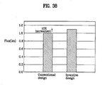
- FIG. 38 depicts flux data of a general light emitting device package and flux data of the light emitting device package according to the tenth embodiment of the present invention. Referring to FIG. 38, it can be seen that an increase in flux by 10% is achieved.
Landscapes
- Led Device Packages (AREA)
- Led Devices (AREA)
Abstract
Description
- The present invention relates to a light emitting device package and a method for manufacturing the same, and more particularly, to a light emitting device package capable of emitting uniform white light and a method for manufacturing the same.
- Light emitting diodes (LEDs) are well known as a semiconductor light emitting device which converts current to light, to emit light. Since a red LED using GaAsP compound semiconductors was made commercially available in 1962, it has been used, together with a GaP:N-based green LED, as a light source in electronic apparatuses, for image display.
- The wavelength of light emitted from such an LED depends on the semiconductor material used to fabricate the LED. This is because the wavelength of the emitted light depends on the band-gap of the semiconductor material representing energy difference between valence-band electrons and conduction-band electrons.
- A gallium nitride (GaN) compound semiconductor has been highlighted in the field of high-power electronic devices including light emitting diodes (LEDs) because it exhibits a high thermal stability and a wide band-gap of 0.8 to 6.2eV. One of the reasons why the GaN compound semiconductor has been highlighted is that it is possible to fabricate semiconductor layers capable of emitting green, blue, and white light, using GaN in combination with other elements, for example, indium (In), aluminum (Al), etc.
- Thus, it is possible to adjust the wavelength of light to be emitted, in accordance with the characteristics of a specific apparatus, using GaN in combination with other appropriate elements. For example, it is possible to fabricate a blue LED useful for optical recording or a white LED capable of replacing a glow lamp.
- Such a white light source may be fabricated using LEDs for emitting light of three primary colors, namely, red, green, and blue, or using an LED for emitting light of a certain color and phosphors.
- In accordance with the method, which uses phosphors, a white light source may be fabricated using a blue LED and yellow phosphors. In this case, white light is produced as blue light emitted from a blue LED and yellow light emitted from yellow phosphors excited by the blue light are mixed.
- Similarly, the white light source may be fabricated using a green LED and red phosphors or using an ultraviolet LED and red, green, and blue phosphors.
- In accordance with the method, which uses a blue LED and yellow phosphors, to fabricate a white light source, red light and green light are emitted as blue light emitted from the blue LED is absorbed in the yellow phosphors in certain degrees. The red light and green light are mixed with the blue light not absorbed in the yellow phosphors, so that they are viewed in the form of white light to the observer.
- The above-mentioned method, which uses a blue LED and yellow phosphors, to fabricate a white light source, are widely used because the fabricated white light source exhibits excellent color rendering, high stability, and high reliability.
- FIG. 1 illustrates an LED lamp which emits white light using the above-mentioned LED and phosphors.
- In the illustrated LED lamp, a
blue LED 3 is disposed on a stack 2 mounted in areflective cup 1. Afiller 5, which is formed by mixingphosphors 4 with a silicon gel or an epoxy resin, is filled in thereflective cup 1 such that thefiller 5 encloses theblue LED 3. Aglass 6 is arranged over thefiller 5. - In this LED lamp structure, however, the
filler 5 enclosing theLED 3 may have a non-uniform thickness. For this reason, there may be an optical path length difference between light paths a and b of light emitted from theLED 3 to the surface of theglass 6. - Accordingly, the present invention is directed to a light emitting device package and a method for manufacturing the same.
- Embodiments of the present invention can provide a light emitting device package capable of emitting light generated from a light source via an external medium while achieving a reduction in optical path length difference, thereby achieving an improvement in the chromatic uniformity at different positions of the light emitting device, and enabling emission of light uniformly changed in wavelength.
- Additional advantages and features of the invention will be set forth in part in the description which follows and in part will become apparent to those having ordinary skill in the art upon examination of the following or may be learned from practice of the invention. The advantages of the invention may be realized and attained by the structure particularly pointed out in the written description and claims hereof as well as the appended drawings.
- A first aspect of the invention provides a light emitting device package comprises: a package body; an electrode formed over at least one surface of the package body; a light emitting device mounted over the package body; and a phosphor layer formed over the light emitting device while having a uniform thickness around the light emitting device.
- Another aspect of the present invention provides a method for manufacturing a light emitting device package comprises: forming a plurality of electrodes over a substrate; bonding light emitting devices to the substrate such that the light emitting devices are connected to the electrodes; forming a phosphor layer over the substrate bonded with the light emitting devices; and dicing the substrate and the phosphor layer into unit packages such that the phosphor layer over an upper surface of the light emitting device in each unit package has a thickness equal to a thickness of the phosphor layer over each side surface of the light emitting device in the unit package.
- Another aspect of the invention provides a method for manufacturing a light emitting device package comprises: forming a barrier rib defining a region surrounding a light emitting device over a mount of a substrate for mounting the light emitting device; mounting the light emitting device over the mount; and filling phosphors inside the barrier rib.
- It is to be understood that both the foregoing general description and the following detailed description of the present invention are exemplary and explanatory and are intended to provide further explanation of the invention as claimed.
- The accompanying drawings, which are included to provide a further understanding of the invention and are incorporated in and constitute a part of this application, illustrate embodiment(s) of the invention and together with the description serve to explain the principle of the invention. In the drawings:
- FIG. 1 is a schematic view illustrating a general light emitting device package;
- FIGs. 2 to 8 are views illustrating a first embodiment of the present invention;
- FIGs. 9 to 13 are views illustrating a second embodiment of the present invention;
- FIGs. 14 to 18 are views illustrating a third embodiment of the present invention;
- FIG. 19 is a view illustrating a fourth embodiment of the present invention;
- FIGs. 20 to 22 are views illustrating a fifth embodiment of the present invention;
- FIGs. 23 to 25 are views illustrating a sixth embodiment of the present invention;
- FIGs. 26 is a view illustrating a seventh embodiment of the present invention;
- FIGs . 27 and 28 are views illustrating an eighth embodiment of the present invention;
- FIGs. 29 to 33 are views illustrating a ninth embodiment of the present invention; and
- FIGs. 34 to 38 are views illustrating a tenth embodiment of the present invention.
- Embodiments of the present invention now will be described more fully hereinafter with reference to the accompanying figures.
- This invention may, however, be embodied in many alternate forms and should not be construed as limited to the embodiments set forth herein. Accordingly, while the invention is susceptible to various modifications and alternative forms, specific embodiments thereof are shown by way of example in the drawings and will herein be described in detail. It should be understood, however, that there is no intent to limit the invention to the particular forms disclosed, but on the contrary, the invention is to cover all modifications, equivalents, and alternatives falling within the scope of the invention as defined by the claims.
- It will be understood that when an element such as a layer, region or substrate is referred to as being "on" another element, it can be directly on the other element or intervening elements may also be present. It will also be understood that if part of an element, such as a surface, is referred to as "inner," it is farther to the outside of the device than other parts of the element.
- In addition, relative terms, such as "beneath" and "overlies", may be used herein to describe one layer's or region's relationship to another layer or region as illustrated in the figures.
- It will be understood that these terms are intended to encompass different orientations of the device in addition to the orientation depicted in the figures. Finally, the term "directly" means that there are no intervening elements. As used herein, the term "and/or" includes any and all combinations of one or more of the associated listed items.
- It will be understood that, although the terms first, second, etc. may be used herein to describe various elements, components, regions, layers and/or sections, these elements, components, regions, layers and/or sections should not be limited by these terms.
- These terms are only used to distinguish one region, layer or section from another region, layer or section. Thus, a first region, layer or section discussed below could be termed a second region, layer or section, and similarly, a second region, layer or section may be termed a first region, layer or section without departing from the teachings of the present invention.
- Hereinafter, a method for manufacturing a light emitting device package according to a first embodiment of the present invention will be described.
- First, a
substrate 10, which is provided with a groove-shaped mount 11 formed at an upper surface of thesubstrate 10, andside grooves 12 formed at opposite side surfaces of thesubstrate 10, is prepared, as shown in FIG. 2. The structure of thesubstrate 10 is also illustrated in FIG. 7. For thesubstrate 10, a silicon substrate or a ceramic substrate may be used. Theside grooves 12 may be formed by forming through holes at opposite sides of thesubstrate 10. - Thereafter, a pair of
electrodes 13 are formed at thesubstrate 10 such that eachelectrode 13 connects the interior of themount 11, an associated one of theside grooves 12, and a lower surface of thesubstrate 10, as shown in FIG. 3. - A
light emitting device 20 is then bonded on thesubstrate 10 inside themount 11 such that thelight emitting device 20 is connected to theelectrodes 13, as shown in FIG. 4. The bonding of thelight emitting device 20 may be achieved usingsolders 21 applied to respective terminals of theelectrodes 13 of thelight emitting device 20. - Subsequently, a
filler 22 is filled in the interior of themount 11 such that thefiller 22 encloses thelight emitting device 20, as shown in FIG. 5. For thefiller 22, a transparent material, which allows light to pass therethrough, may be used. For example, a silicon gel or an epoxy resin may be used. - A
resin layer 23, in which phosphors are uniformly distributed, is the formed over thefiller 22, as shown in FIG. 6. Theresin layer 23 may have a uniform thickness. Thus, a light emitting device package is completely manufactured. - In the light emitting device package manufactured as described above, light generated from the
light emitting device 20 passes through theresin layer 23, which has a uniform thickness and is dispersed with phosphors, so that the wavelength of the light is uniformly changed. Accordingly, the wavelength-changed light is emitted from the light emitting device package. - For example, where the
light emitting device 20 is a blue light emitting device, and the phosphors dispersed in theresin layer 23 are yellow phosphors, blue light generated from the bluelight emitting device 20 is mixed with yellow light generated from the yellow phosphors while passing through theresin layer 23. In accordance with the mixing of blue and yellow colors, white light may be emitted from the light emitting device package. - As described above, the
mount 11 is formed at the upper surface of thesubstrate 10. Also, theside grooves 12 are formed at opposite sides of themount 11. - In order to smoothly form the
electrodes 13, each side surface of thesubstrate 10 has a centrally-protruded shape by inclinedly etching upper and lower portions of the side surface upon forming the associatedside groove 12. - The
mount 11 also has inclined side walls, so that light emitted from thelight emitting device 10 mounted on the bottom surface of themount 11 can be reflected from the inclined side walls. In this case, it is possible to increase the amount of light output through the top of the package. - FIG. 8 illustrates optical travel paths in the light emitting device package according to this embodiment. As shown in FIG. 8, light emerging from the top of the
light emitting device 20 mounted on the bottom surface of themount 11 travels along an optical path B, whereas light emerging from each side surface of thelight emitting device 20 travels along an optical path A after being reflected by the side surface of themount 11 facing the side surface of thelight emitting device 20. - Accordingly, the light traveling along the optical path A and the light traveling along the optical path B passes through the phosphor-distributed
resin layer 23, which has a uniform thickness, so that the wavelength of the light is uniformly changed. - Hereinafter, a method for manufacturing a light emitting device package according to a second embodiment of the present invention will be described.
- As shown in FIG. 9, a mounting
recess 31 is first formed at an upper surface of asubstrate 30. A pair ofelectrodes 32 are then formed in the mountingrecess 31 such that theelectrodes 32 extend along side walls of the mountingrecess 31 and then extend along the upper surface of thesubstrate 30. - A
light emitting device 40 is then bonded on the substrate to portions of theelectrodes 32 arranged in the mountingrecess 31, as shown in FIG. 10. Subsequently, afiller 42 is filled in the mountingrecess 31. A phosphor-distributedresin layer 43 is the formed over the mountingrecess 31 filled with thefiller 42. - The bonding of the
light emitting device 40 may be achieved by bonding terminals of thelight emitting device 40 to theelectrodes 32 usingsolders 41, as in the first embodiment as described above. - The filling of the
filler 42 may be achieved using a dispensing method, as shown in FIG. 11. In accordance with the dispensing method, anozzle 82, which contains thefiller 42, is positioned in the mountingrecess 31 above thelight emitting device 40. Thefiller 42 is then discharged from thenozzle 82, to fill the mountingrecess 31. - The formation of the
resin layer 43 over thefiller 42 may be achieved using a screen printing process, as shown in FIG. 12. - In accordance with the screen printing process, a
stencil 80 having an opening is first prepared. Thestencil 80 is then arranged on thefiller 42 such that thefiller 42 is exposed through the opening of thestencil 80. Thereafter, a phosphor-distributed resin material is supplied to the opening of thestencil 80 such that the resin material is applied to thefiller 42. The resin material is then spread using asqueegee 81 arranged over thestencil 80 such that the resin material forms a film. - Using the above-described screen printing process, it is possible to form the phosphor-distributed
resin layer 43 on thefiller 42 in the form of a film having a uniform thickness. - Meanwhile, the
resin layer 43 may be formed by separately preparing a phosphor-distributed resin film, and attaching the resin film to an upper surface of thefiller 42, as shown in FIG. 13. - The remaining configurations of the second embodiment may be identical to those of the first embodiment, and so, no description thereof will be given.
- Hereinafter, a method for manufacturing a light emitting device package according to a third embodiment of the present invention will be described.
- As shown in FIG. 14, a pair of
electrodes 51 are formed at opposite sides of afirst substrate 50 such that the upper and lower surfaces of thefirst substrate 50 are connected by eachelectrode 51. - A
second substrate 52, which includes a mountinghole 53, as shown in FIG. 15, is prepared. - It is preferred that a reflective film is formed on the mounting
hole 53 of thesecond substrate 52. The reflective film functions to reflect light emerging from a light emitting device, which will be mounted in a subsequent process, and thus to increase the amount of light emitted through the top of the package. - As shown in FIG. 16, the
second substrate 52 is attached to thefirst substrate 50 such that theelectrodes 51 are partially exposed through the mountinghole 53. The substrate attachment may be achieved using an adhesive 54 such as an adhesive resin or an adhesive tape. - Thereafter, a
light emitting device 60 is bonded to theelectrodes 51 exposed through the mountinghole 53 of thesecond substrate 52, as shown in FIG. 17. Afiller 62 is then filled in the mountinghole 53. - Subsequently, a phosphor-distributed
resin layer 63 is formed over thefiller 62, as shown in FIG. 18. - For each of the first and
second substrates - FIG. 19 illustrates a light emitting device package according to a fourth embodiment of the present invention. In particular, FIG. 19 shows a state in which a
zener diode 73 is mounted together with alight emitting device 72, to achieve an improvement in voltage withstand characteristics. - In accordance with this embodiment, the
light emitting device 72 andzener diode 73 are bonded using wires in a state in which a pair ofleads filler 75 is formed over thelight emitting device 72 andzener diode 73. A phosphor-distributedresin layer 76 is also formed over thefiller 75. - Where a package is configured by connecting the
zener diode 73 and light emittingdevice 72 in parallel, as described above, over-current generated when a surge voltage is applied to thelight emitting device 72, which exhibits inferior voltage withstand characteristics, namely, inferior resistance to static electricity, does not flow toward thelight emitting device 72. That is, a zener breakdown occurs in thezener diode 73 near a zener voltage due to the over-current, thereby causing the over-current to be bypassed through thezener diode 73. Thus, thelight emitting device 72 is protected from the over-current. - FIGs. 20 to 22 illustrate procedures for manufacturing a light emitting device package according to a fifth embodiment of the present invention.
- In accordance with the fifth embodiment, through
holes 110 are first formed through asubstrate 100 using a laser or an etching method, as shown in FIG. 20. Thesubstrate 100 may be one of a ceramic substrate or a silicon substrate to be used for a 2D sub-mount or a package for a light emitting device. - The
substrate 100, which is formed with the throughholes 110, as described above, forms a package body. - Thereafter,
electrodes 200 to be connected tomounts 120, on which light emitting devices will be mounted, are formed on the surface of thesubstrate 100. - Each
electrode 200 has a structure connected between the front and back surfaces of thesubstrate 100 using a metal line. That is, eachelectrode 200 includes a front-side electrode 210 connected to a light emitting device, and a back-side electrode 220 formed at the back surface of thesubstrate 100 and connected to the front-side electrode 210 via one throughhole 110. - The back-
side electrode 220 may be electrically connected to an external circuit functioning to supply current to a light emitting device. In this case, it is preferred that the throughholes 110 be formed in an isolation region of the package. - Uniformly-spaced
barrier ribs 300 exhibiting excellent light transmissivity are formed at the front surface of thesubstrate 100, on which light emittingdevices 400 will be mounted. - The
barrier ribs 300 may be made of a photosensitive polymer. That is, the formation of thebarrier ribs 300 can be achieved by coating a photosensitive polymer over the front surface of thesubstrate 100, and performing a photolithography process such that the photosensitive polymer remains in a region where thebarrier ribs 300 will be formed, while being removed in other regions. - Alternatively, the
barrier ribs 300 may be formed by separately fabricating barrier ribs using a material exhibiting excellent light transmissivity, for example, glass, and bonding the fabricated barrier ribs to thesubstrate 100. - After the manufacture of the sub-mount or package as described above, the
light emitting devices 400 are bonded to the sub-mount or package, as shown in FIG. 21. - A
filler 310, such as a phosphor-containing epoxy resin or silicon gel, is then filled in spaces between thebarrier ribs 300 and thelight emitting devices 400, as shown in FIG. 22. - It is preferred that the height difference between each
barrier rib 300 and the upper surface of each light emittingdevice 400 be equal to the distance between thebarrier rib 300 and the side surface of thelight emitting device 400 facing thebarrier rib 300. - Accordingly, there is no optical path length difference between light emitted from the side surface of the
light emitting device 400 along a path A in FIG. 22 and light emitted from the upper surface of thelight emitting device 400 along a path B in FIG. 22. Thus, a uniform light distribution is obtained. - For each light emitting
device 400, any of a horizontal type light emitting device and a vertical type light emitting device can be used. - Subsequently, lenses (not shown) may be mounted to the
substrate 100 packaged with thelight emitting devices 400. Thesubstrate 100 is then divided into individual packages. - FIGs. 23 to 25 illustrate procedures for manufacturing a light emitting device package according to a sixth embodiment of the present invention.
- In accordance with the sixth embodiment, through
holes 110 are first formed through asilicon substrate 100 using a solution enabling anisotropic etching, for example, a KOH or tetramethyl ammonium hydroxide (TMAH) solution, as shown in FIG. 23. Thesubstrate 100 may be used for a sub-mount or a package for a light emitting device. - Where the through
holes 110 are formed in accordance with an etching process, as described above, they have a structure as shown in FIG. 23. The etching for the formation of the throughholes 110 is carried out at both the front and back surfaces of thesubstrate 100 such that the etched front and back portions of thesubstrate 100 to form each throughhole 110 are connected. - Thereafter,
electrodes 200 to be connected tomounts 120, on which light emitting devices will be mounted, are formed on the surface of thesubstrate 100. - As in the fifth embodiment described above, each
electrode 200 may include a front-side electrode 210 connected to a light emitting device, and a back-side electrode 220 formed at the back surface of thesubstrate 100 and connected to the front-side electrode 210 via one throughhole 110. - Subsequently,
barrier ribs 300 are formed, and light emittingdevices 400 are mounted to themounts 120, as shown in FIG. 24. - A
filler 310 is then filled in spaces defined by thebarrier ribs 300 inside thebarrier ribs 300, as shown in FIG. 25. Subsequent procedures are identical to those of the fifth embodiment. - FIG. 26 illustrates a light emitting device package according to a seventh embodiment of the present invention.
- In the illustrated light emitting device, a
light emitting device 400 is bonded to analuminum slug 130 having a mirror surface, using an adhesive 140. Abarrier rib 300 is formed around thelight emitting device 400, using a material exhibiting excellent light transmissivity. - A
filler 310, such as a phosphor-containing epoxy resin or silicon gel, is filled between thebarrier rib 300 and thelight emitting device 400. - The electrodes of the
light emitting device 400 is electrically connected to leads 150 fixed to apackage body 101, usingconductive wires 160. - A
lens 170 is formed on or directly attached to an upper surface of thepackage body 101, on which thelight emitting device 400 is mounted. - It is preferred that the height difference between the
barrier rib 300 and the upper surface of thelight emitting device 400 be equal to the distance between thebarrier rib 300 and the side surface of thelight emitting device 400 facing thebarrier rib 300. - FIGs. 27 and 28 illustrate procedures for manufacturing a light emitting device package according to an eighth embodiment of the present invention.
- In accordance with this embodiment, through
holes 110 are first formed through asubstrate 100 using a laser or an etching method, as shown in FIG. 27. Thesubstrate 100 may be one of a ceramic substrate or a silicon substrate to be used for a sub-mount or a package for a light emitting device.Mounts 120, on which light emitting devices will be mounted, are also formed at thesubstrate 100 - As shown in FIG. 27, each
mount 120 has a recess structure formed as thesubstrate 100 is recessed in accordance with an etching process. By virtue of such a structure, eachmount 120 can upwardly reflect light emitted from each side surface of the light emitting device. - The
substrate 100, which is formed with the throughholes 110, as described above, forms a package body. - Thereafter,
electrodes 200 are formed on thesubstrate 100 such that eachelectrode 200 has a structure connected between the front and back surfaces of thesubstrate 100 using a metal line. - In this case, it is preferred that the through
holes 110 be formed in an isolation region of the package. - Uniformly-spaced
barrier ribs 300 exhibiting excellent light transmissivity are formed at the front surface of thesubstrate 100, on which light emittingdevices 400 will be mounted. - The
barrier ribs 300 may be made of a photosensitive polymer. That is, the formation of thebarrier ribs 300 can be achieved by coating a photosensitive polymer over the front surface of thesubstrate 100, and performing a photolithography process such that the photosensitive polymer remains in a region where thebarrier ribs 300 will be formed, while being removed in other regions. Alternatively, thebarrier ribs 300 may be formed by separately fabricating barrier ribs using a material exhibiting excellent light transmissivity, for example, glass, and bonding the fabricated barrier ribs to thesubstrate 100. - After the manufacture of the sub-mount or package as described above, the
light emitting devices 400 are mounted to the sub-mount or package in accordance with, for example, a flip chip bonding process. - That is, each light emitting
device 400 may be bonded to the associatedelectrode 200 in a state in which thelight emitting device 400 has a structure inverted from a horizontal structure. In this case, a zener diode (not shown) may be provided at theelectrode 200. - Thereafter, a
filler 310, such as a phosphor-containing epoxy resin or silicon gel, is filled in spaces between thebarrier ribs 300 and thelight emitting devices 400, as shown in FIG. 22. - It is preferred that the height difference between each
barrier rib 300 and the upper surface of each light emittingdevice 400 be equal to the distance between thebarrier rib 300 and the side surface of thelight emitting device 400 facing thebarrier rib 300. - Accordingly, the lengths of the optical paths of light beams emitted from the
light emitting device 400 through phosphors are substantially equal, as in the above-described embodiments. - The light emitted from each side surface of the
light emitting device 400 is changed in wavelength while passing through the phosphors. In this case, the emitted light then passes through thebarrier rib 300 because the barrier rib 330 exhibits excellent light transmissivity. The light emerging from the barrier rib 330 is then reflected by aside wall 121 of themount 120 such that it is upwardly directed. - A separate reflective film (not shown) may be formed on the
side wall 121 of themount 120. - <Ninth Embodiment>
- In a procedure for manufacturing a light emitting device package in accordance with a ninth embodiment of the present invention,
electrodes 520, each of which includes a pair of electrode structures, are formed on asubstrate 500, as shown in FIG. 29. - Each
electrode 520 may include an upper electrode (front-side electrode) 521, to which a light emitting device will be coupled at desired electrical and structural strengths, and a lower electrode (back-side electrode) 522, which will be coupled to a structure for supplying an external voltage, for example, a printed circuit board (PCB) substrate, at desired electrical and structural strengths. - The
upper electrode 521 andlower electrode 522 of eachelectrode 520 may be connected by a connectingelectrode 523 formed in a throughhole 510. The throughhole 510 may be formed through thesubstrate 500 in accordance with a bulk etching process. - For the formation of the
electrodes 520 on thesubstrate 500, a mask layer (not shown) is first formed on thesubstrate 500. Alternatively, a mask pattern required for bulk-etching of regions, where throughholes 510 will be formed, is formed on thesubstrate 500 in a state in which a mask layer has been formed on thesubstrate 500. - Using the mask pattern, the
substrate 500 is bulk-etched (bulk-micromachined), to form the throughholes 510. - The
substrate 500 may include a silicon substrate, or substrates made of other materials, namely, aluminum, aluminum nitride (A1N), aluminum oxide (AlOx), photo sensitive glass (PSG), Al2O3, BeO, or PCB. - For the bulk-etching process, which is adapted to form the through
holes 510, a wet etching process, a dry etching process, or a laser drilling process may be used. - A representative of the dry etching process may be a dip reactive ion etching process.
- In the etching process for the formation of the through
holes 510, a mask layer (not shown) is needed to define a region to be etched and a region to be prevented from being etched. The mask layer should be made of a material capable of exhibiting a mask function for a prolonged period of time in a dry or wet etching process. For the mask layer, a silicon nitride film or a silicon oxide film may be used. - Meanwhile, in order to divide the
upper electrodes 521 into positive and negative electrodes and to divide thelower electrodes 522 into positive and negative electrodes, it is preferred that the throughholes 510, each of which electrically connects the upper andlower electrodes electrode 520, be divided into two groups of through holes, namely, through holes for positive electrodes and through holes for negative electrodes. - Thereafter, an insulation layer for electrical insulation (not shown) is formed on the overall surface of the
substrate 500. For the formation of the insulation layer, the mask layer (not shown) used to form the throughholes 510 is removed in this embodiment. A silicon oxide film exhibiting excellent insulation characteristics is then formed on the overall surface of thesubstrate 500 in accordance with a thermal oxidation method. - A silicon nitride film may be deposited for the insulation layer (not shown), using an insulation layer formation method other than the above-described method, for example, a low pressure chemical vapor deposition (LPCVD) method or a plasma enhanced chemical vapor deposition (PECVD) method.
- The insulation layer may be dispensed with in the case in which the
substrate 500 is made of an insulation material such as an aluminum nitride (AlN) or an aluminum oxide (AlOx). - Thereafter, the formation of the
electrodes 520 on the structure formed with the throughholes 510 is carried out in accordance with a patterning process. - For the formation of the
electrodes 520, which are laterally separated from one another, a photoresist is first coated over the front or back surface of thesubstrate 500. Light exposure and development are then carried out. - A metal for the formation of the
electrodes 520 is then deposited on the front or back surface of thesubstrate 500 in accordance with a sputtering method or an E-beam evaporation method. Before the deposition of the metal, a seed metal may be deposited. - The deposited metal is then lifted off, to form the
electrodes 520 on the front or back surface of thesubstrate 500. - Thereafter, a seed metal (not shown) is deposited over the surface of the
substrate 500 opposite to the metal-deposited surface. Theelectrodes 520 are then formed on the seed metal. Subsequently, photoresist coating, light exposure, and development are sequentially carried out, to separate theelectrodes 520 into positive and negative electrodes. - A patterning process is then carried out to form connecting
electrodes 523 in the throughholes 510 in accordance with an electroplating method or an electroless-plating method, and thus to connect the front-side electrodes 521 and the back-side electrodes 522 via the connectingelectrodes 523. - Meanwhile, the seed metal may be etched to separate adjacent ones of the
electrodes - Gold (Au), copper (Cu), or aluminum (Al) may be used which is a representative electrode metal exhibiting excellent electrical characteristics while being easily depositable in a semiconductor process.
- The electrode metal is exposed to a high temperature condition in a subsequent procedure, in particular, a process for coupling module elements. For this reason, Ti or Cr, which is the material of the adhesion layer, may be diffused into Au, thereby degrading the electrical characteristics of Au. To this end, a diffusion barrier layer made of, for example, platinum (Pt) or nickel (Ni), may be interposed between the adhesion layer of Ti or Cr and the Au layer. Thus, the
electrodes 520 may have a structure of Ti/Pt/Au, Cr/Ni/Au, or Cr/Cu/Ni/Au. - After the formation of the
electrodes 520, areflective layer 530 may be formed on the upper surface of thesubstrate 500, in order to achieve an enhancement in the extraction efficiency of light emitted from the light emitting device, which will be subsequently mounted. - The
reflective layer 530 may be made of a material exhibiting an excellent reflectivity, for example, aluminum (Al) or silver (Ag). - The formation of the
reflective layer 530 may be achieved by coating a photoresist over the upper surface of thesubstrate 500, patterning the coated photoresist in accordance with light exposure and development such that the bottom surface thesubstrate 500, on which the light emitting device will be mounted, is exposed, depositing a reflective material in accordance with a sputtering method or an E-beam evaporation method, and lifting off the patterned photoresist. - Alternatively, the
reflective layer 530 may be formed by depositing a reflective material over the upper surface of thesubstrate 500, and then etching unnecessary portions of the deposited reflective material. - The
reflection layer 530 should be formed to prevent it from being connected to or overlapped with both the electrodes of each electrode pair, in order to prevent electrical short circuit. In order to enable thereflective layer 530 to adhere to theelectrodes 520 of the light emitting devices, it is also preferred that thereflective layer 530 should not be present on theelectrodes 520 in regions where solders or Au stud pumps 611 (FIG. 31) will be formed. - Hereinafter, subsequent procedures will be described in conjunction with the case in which the
reflective film 530 is not formed. - Next, a plurality of light emitting
devices 610 are bonded to respective pairs of theelectrodes 520, in accordance with a bonding method using conductive solders orAu studs 611, as shown in FIG. 31A. - FIG. 31A illustrates the case in which the
light emitting devices 610 are flip-chip-bonded. If necessary, horizontal or vertical type light emitting devices may be wire-bonded. - Thereafter, a
phosphor layer 620 are uniformly formed over thesubstrate 500, to which thelight emitting devices 610 have been bonded, such that thephosphor layer 620 covers all the light emittingdevices 610. - The
phosphor layer 520 may be made of a material consisting of a transparent medium and phosphor powder contained in the transparent medium. For the transparent medium, a resin material, such as an epoxy resin or a silicon gel, may be used. - The phosphor powder may be a phosphor material which absorbs light emitted from the
light emitting devices 610, and emits light having energy lower than that of the light emitted from thelight emitting devices 610. For example, the phosphor powder may be a yellow phosphor material emitting yellow light. Eachlight emitting device 610 may be a blue light emitting device. In this case, white light can be emitted in accordance with a mixture of the light emitted from the blue light emitting device and the light emitted from the yellow phosphor material. - The
phosphor layer 620 is evenly filled such that it has a constant thickness W1 over the upper surface of each light emittingdevice 610. Also, the spacing W4 between the adjacentlight emitting devices 610 is also adjusted such that thephosphor layer 620 is formed to have a uniform thickness on all the light emitting surfaces of each light emittingdevice 610, namely, the upper and side surfaces of each light emitting device 610 (W1 = W2 = W3). - The spacing W4 between the adjacent
light emitting devices 610 may be determined, taking into consideration the width D1 of a portion of thesubstrate 500 orphosphor layer 620 to be removed betweenadjacent packages 600 when the package structure including thesubstrate 500 andphosphor layer 620 is diced intoindividual packages 600. - The spacing W4 between the adjacent
light emitting devices 610 may correspond to a length obtained by adding the width D1, to be removed in the dicing process, to two times the thickness of thephosphor layer 620 present on the upper surface of each light emitting device 610 (W4 = 2 x W1 + D1). - Accordingly, the spacing W4 between the adjacent
light emitting devices 610 may correspond to a length obtained by adding the width D1, to be removed in the dicing process, to two times the distance W1, W2, or W3 between the outer surface of thelight emitting device 610 and the outer surface of thephosphor layer 620 in each diced package 600 (W4 = 2 x W1 + D1 = 2 x W2 + D1 = 2 x W3 + D1, or W4 = W2 + W3 + D1) . - If the width D1, to be removed between the
adjacent packages 600 in the dicing process, is negligible, the spacing W4 between the adjacentlight emitting devices 610 may substantially correspond to two times the distance W1, W2, or W3 between the outer surface of thelight emitting device 610 and the outer surface of thephosphor layer 620 in each diced package 600 (W4 = 2 x W1 = 2 x W2 = 2 x W3, or W4 = W2 + W3). - In this case, accordingly, the spacing W4 between the adjacent
light emitting devices 610 may substantially correspond to two times the thickness W1 of thephosphor layer 620 over the upper surface of each light emitting device 610 (W4 = 2 x W1). - Meanwhile, the
phosphor layer 620 may be made of a mixture of a silicon gel or an epoxy resin having excellent light transmissivity and phosphor powder. - The solders for bonding of the
light emitting devices 610 may be formed, using gold-tin (AuSn), lead-tin (PbSn), or indium (In), in accordance with an E-beam evaporation method. - Meanwhile, the package structure may be diced such that a plurality of light emitting
devices 610 constitute one package, as shown in FIG. 31B. For example, the package structure may be diced such that four light emittingdevices 610 constitute one package, as shown in FIG. 31B. Of course, each package may include two, six, or other numbers of light emittingdevices 610. - In such cases, the spacing between the adjacent
light emitting devices 610 may be different from that of FIG. 31A. In such cases, the spacing W5 betweenadjacent package 600 satisfies the above-described conditions. - For example, where four light emitting
devices 610 constitute onepackage 600, the spacing W5 between theadjacent packages 600 may correspond to two times the distance W2 or W3 between the outer surface of each light emittingdevice 610 and the outer surface of thephosphor layer 620 in each dicedpackage 600. - In this case, the spacing W5 between the
adjacent packages 600 may correspond to two times the thickness W1 of thephosphor layer 620 over the upper surface of each light emittingdevice 610. - On the other hand, when the spacing W5 between the
adjacent packages 600 is determined, taking into consideration the width (not shown) to be removed between theadjacent package 600 in the dicing process, the spacing W5 may correspond to a length obtained by adding the width, to be removed between theadjacent package 600 in the dicing process, to two times the distance W2 or W3 between the outer surface of each light emittingdevice 610 and the outer surface of thephosphor layer 620 in each dicedpackage 600. - In this case, the spacing W5 between the
adjacent packages 600 may correspond to a length obtained by adding the width, to be removed in the dicing process, to two times the thickness of thephosphor layer 620 present on the upper surface of each light emittingdevice 610. - Thereafter, as shown in FIG. 32, the light emitting device package structure in a wafer size is diced into
individual packages 600 such that the phosphor layer is present on the upper and side surfaces of thelight emitting device 610 in eachpackage 600 while having a uniform thickness (W1 = W2 = W3). - The
individual packages 600, which are obtained in accordance with the dicing process, may be bonded to aPCB substrate 630 at desired electrical and structural strengths, so as to be used for various purposes, for example, backlight units or illumination lamps. - If necessary, each
package 600 may include alens 640 having a shape designed to control the distribution of light emitted from thelight emitting device 610 or to achieve an enhancement in light efficiency, as shown in FIG. 33. - <Tenth Embodiment>
- In a package according to a tenth embodiment of the present invention, as shown in FIG. 34, a
light emitting device 800 is mounted to apackage body 700 formed with amount 710. - The
package body 700 includes an upper frame made of a plastic material and coupled to alead 720, and alower frame 740 arranged beneath themount 710 and coupled to theupper frame 730. - The
lower frame 740 is made of a conductive material such as aluminum, in order to function as a heat sink. - In this structure, the
light emitting device 800 is electrically connected to thelead 720 via awire 810. Afiller 820 is filled in themount 710, on which thelight emitting device 800 is mounted. Thefiller 820 may contain phosphors. - For example, phosphors may be mixed with an epoxy resin or silicon gel, and the resulting mixture is filled in the
mount 710, as thefiller 820. - For an example of a combination of the
light emitting device 800 and phosphors, a blue light emitting device, which emits blue light, may be used for thelight emitting device 800, and phosphors, which partially absorbs the blue light, thereby emitting yellow light, may be used. In this case, it is possible to realize a white light emitting device package capable of emitting white light in accordance with a mixture of blue light and yellow light. For the bluelight emitting device 800, a gallium nitride (GaN)-based light emitting device may be used. In addition, light emitting devices and phosphors emitting light of various colors may be used. - A
lens 830 may be arranged over themount 710 filled with thefiller 820. - FIG. 35 is an enlarged view showing the
mount 710, on which thelight emitting device 800 is mounted. - As shown in FIGs. 36 and 37, the
mount 710, on which thelight emitting device 800 is mounted, is formed such that the height X from the upper surface of thelight emitting device 800 is equal to a horizontal distance X between each outer side surface of thelight emitting device 800 and the inner side surface of themount 710 facing the outer side surface of thelight emitting device 800 at the bottom of themount 710. - That is, the depth of the
mount 710 is determined such that the height of themount 710 from the upper surface of thelight emitting device 810 is equal to "X", and the width of themount 710 is determined such that the horizontal distance between each outer side surface of thelight emitting device 800 and the inner side surface of themount 710 facing the outer side surface of thelight emitting device 800 at the bottom of themount 710 is equal to "X". - Where the
light emitting device 800 has a square shape having four side surfaces, themount 710 may be formed such that the width of themount 710 is determined such that the horizontal distance between each of the four side surface of thelight emitting device 800 and the side surface of themount 710 facing the side surface of thelight emitting device 800 at the bottom of themount 710 is equal to "X". - Taking into consideration the fact that the
light emitting device 800 typically has a height of about 100µm, a length of about 1mm, and a width of about 1mm, it is preferred that the depth of themount 710 be 0.2 to 0.6mm. It is also preferred that the length and width of themount 710 be 1.2 to 2mm. - That is, the depth of the
mount 710 may be 2 to 6 times the height of thelight emitting device 800. Also, the length or width of themount 710 may be 1.2 to 2 times the length or width of thelight emitting device 800. - The height of the
mount 710 from the upper surface of thelight emitting device 800 may be 1 to 5 times the height of thelight emitting device 800. The horizontal distance between themount 710 and thelight emitting device 800 may be 0.1 to 0.5 times the length or width of thelight emitting device 800. - The inner side surfaces of the
mount 710 may be included to have a certain inclination θ. It is preferred that the inclination of the side surfaces of themount 710 be 0 to 30° from a virtual vertical line. - FIG. 38 depicts flux data of a general light emitting device package and flux data of the light emitting device package according to the tenth embodiment of the present invention. Referring to FIG. 38, it can be seen that an increase in flux by 10% is achieved.
- It will be apparent to those skilled in the art that various modifications and variations can be made in the present invention without departing from the scope of the invention. Thus, it is intended that the present invention covers the modifications and variations of this invention provided they come within the scope of the appended claims.
Claims (20)
- A light emitting device package comprising:a package body;an electrode formed over at least one surface of the package body;a light emitting device mounted over the package body; anda phosphor layer formed over the light emitting device while having a uniform thickness around the light emitting device.
- The light emitting device package according to claim 1, wherein the thickness of the phosphor layer arranged over an upper surface of the light emitting device is equal to the thickness of the phosphor layer arranged on each side surface of the light emitting device.
- The light emitting device package according to claim 1, wherein the phosphor layer has a horizontal width equal to a horizontal width of the package body.
- The light emitting device package according to claim 1, wherein the electrode comprises:an upper electrode formed over an upper surface of the package body; anda lower electrode formed over a lower surface of the package body, and connected to the upper electrode.
- The light emitting device package according to claim 4, wherein the upper and lower electrodes are connected via a through hole formed through the package body.
- The light emitting device package according to claim 1, wherein the phosphor layer is arranged inside a transparent barrier rib arranged around the light emitting device while being uniformly spaced apart from the light emitting device.
- The light emitting device package according to claim 6, wherein the barrier rib is made of one of a transparent photoresist, a photosensitive polymer, and glass.
- The light emitting device package according to claim 6, wherein the barrier rib has a height difference from an upper surface of the light emitting device, the height difference being equal to a distance between each side surface of the light emitting device and the barrier rib.
- The light emitting device package according to claim 1, wherein the phosphor layer is made of a filler containing phosphors.
- The light emitting device package according to claim 1, wherein the light emitting device is mounted to a recess-shaped mount formed at the package body.
- The light emitting device package according to claim 10, wherein the mount has a height from an upper surface of the light emitting device, the height being equal to a horizontal distance of the mount from each side surface of the light emitting device.
- The light emitting device package according to claim 10, wherein the mount has a depth equal to 2 to 6 times a height of the light emitting device.
- The light emitting device package according to claim 10, wherein the mount has a horizontal or vertical length equal to 1.2 to 2 times a horizontal or vertical width of the light emitting device.
- A method for manufacturing a light emitting device package, comprising:forming a plurality of electrodes over a substrate;bonding light emitting devices to the substrate such that the light emitting devices are connected to the electrodes;forming a phosphor layer over the substrate bonded with the light emitting devices; anddicing the substrate and the phosphor layer into unit packages such that the phosphor layer over an upper surface of the light emitting device in each unit package has a thickness equal to a thickness of the phosphor layer over each side surface of the light emitting device in the unit package.
- The method according to claim 14, wherein a spacing between adjacent ones of the light emitting devices is equal to two times the thickness of the phosphor layer present over the upper surface of each light emitting device or is equal to a length obtained by adding a width removed at the dicing step to two times the thickness of the phosphor layer present over the upper surface of each light emitting device.
- The method according to claim 14, wherein each unit package includes a plurality of light emitting devices.
- A method for manufacturing a light emitting device package, comprising:forming a barrier rib defining a region surrounding a light emitting device over a mount of a substrate for mounting the light emitting device;mounting the light emitting device over the mount; andfilling phosphors inside the barrier rib.
- The method according to claim 17, further comprising:forming electrodes on the substrate before the formation of the barrier rib.
- The method according to claim 17, wherein the formation of the barrier rib is carried out by coating a photosensitive polymer over the substrate, and etching the coated photosensitive polymer in accordance with a photolithography process.
- The method according to claim 17, wherein the formation of the barrier rib is carried out by preparing a barrier rib made of a transparent material, and attaching the prepared barrier rib to the substrate.
Applications Claiming Priority (3)
| Application Number | Priority Date | Filing Date | Title |
|---|---|---|---|
| KR20060074751A KR101163492B1 (en) | 2006-08-08 | 2006-08-08 | LED package |
| KR20060078635A KR100845864B1 (en) | 2006-08-21 | 2006-08-21 | Light emitting device package and its manufacturing method |
| KR20060130114A KR100866879B1 (en) | 2006-12-19 | 2006-12-19 | Light emitting device package and its manufacturing method |
Publications (3)
| Publication Number | Publication Date |
|---|---|
| EP1887637A2 true EP1887637A2 (en) | 2008-02-13 |
| EP1887637A3 EP1887637A3 (en) | 2010-09-15 |
| EP1887637B1 EP1887637B1 (en) | 2016-12-14 |
Family
ID=38616342
Family Applications (1)
| Application Number | Title | Priority Date | Filing Date |
|---|---|---|---|
| EP07253107.2A Not-in-force EP1887637B1 (en) | 2006-08-08 | 2007-08-08 | Light emitting diode package |
Country Status (4)
| Country | Link |
|---|---|
| US (3) | US20080035942A1 (en) |
| EP (1) | EP1887637B1 (en) |
| JP (3) | JP2008042211A (en) |
| TW (1) | TWI418054B (en) |
Cited By (8)
| Publication number | Priority date | Publication date | Assignee | Title |
|---|---|---|---|---|
| CN102403422A (en) * | 2011-11-17 | 2012-04-04 | 深圳市天电光电科技有限公司 | Processing method of LED packaging structure and LED packaging structure |
| EP2312656A3 (en) * | 2009-10-19 | 2012-07-18 | LG Innotek Co., Ltd. | Light emitting apparatus and lighting system |
| CN102620155A (en) * | 2011-01-26 | 2012-08-01 | Nlt科技股份有限公司 | Light source unit and device using same |
| EP2249403A4 (en) * | 2008-02-25 | 2013-03-06 | He Shan Lide Electronic Entpr Company Ltd | METHOD FOR MANUFACTURING LED APPARATUS |
| EP2309558A3 (en) * | 2009-10-12 | 2014-05-14 | InterLight Optotech Corporation | Light emitting diode and manufacturing method thereof |
| CN105090902A (en) * | 2014-05-06 | 2015-11-25 | 奇想创造事业股份有限公司 | Plastic lamp holder with mounting surface provided with separation groove and plastic bulb with lamp holder |
| CN109742212A (en) * | 2018-12-21 | 2019-05-10 | 华中科技大学鄂州工业技术研究院 | A kind of LED encapsulation structure and packaging method |
| EP2526572B1 (en) * | 2010-01-19 | 2019-08-14 | LG Innotek Co., Ltd. | Package and manufacturing method of the same |
Families Citing this family (57)
| Publication number | Priority date | Publication date | Assignee | Title |
|---|---|---|---|---|
| TWI418054B (en) * | 2006-08-08 | 2013-12-01 | Lg電子股份有限公司 | Light emitting device package and method of manufacturing the same |
| US8283683B2 (en) * | 2006-11-07 | 2012-10-09 | Opto Tech Corporation | Chip-bonding light emitting diode chip |
| US7915061B2 (en) * | 2007-05-31 | 2011-03-29 | GE Lighting Solutions, LLC | Environmentally robust lighting devices and methods of manufacturing same |
| CN101577300A (en) * | 2008-05-08 | 2009-11-11 | 先进开发光电股份有限公司 | Light emitting diode and packaging method thereof |
| KR100982989B1 (en) * | 2008-05-19 | 2010-09-17 | 삼성엘이디 주식회사 | Light emitting diode package |
| TWI475718B (en) * | 2008-05-21 | 2015-03-01 | 榮創能源科技股份有限公司 | Light-emitting diode and packaging method thereof |
| US20100117106A1 (en) * | 2008-11-07 | 2010-05-13 | Ledengin, Inc. | Led with light-conversion layer |
| KR101515426B1 (en) * | 2008-11-11 | 2015-04-27 | 삼성디스플레이 주식회사 | Backlight assembly, Liquid crystal display device comprising the backlight assembly, and method of fabricating the same |
| KR101020993B1 (en) * | 2009-03-10 | 2011-03-09 | 엘지이노텍 주식회사 | Light emitting device package and its manufacturing method |
| KR101081055B1 (en) * | 2009-07-24 | 2011-11-07 | 엘지이노텍 주식회사 | Light emitting device package and method for fabricating the same |
| KR101124102B1 (en) * | 2009-08-24 | 2012-03-21 | 삼성전기주식회사 | Substrate for light emitting device package and light emitting device package comprising the same |
| TW201110430A (en) * | 2009-09-04 | 2011-03-16 | yi-zhang Chen | Heat dissipation substrate of light-emitting diode and its manufacturing method thereof |
| DE102009051746A1 (en) * | 2009-09-30 | 2011-03-31 | Osram Opto Semiconductors Gmbh | Optoelectronic component |
| JP5526712B2 (en) * | 2009-11-05 | 2014-06-18 | 豊田合成株式会社 | Semiconductor light emitting device |
| DE102009053064A1 (en) * | 2009-11-13 | 2011-05-19 | Osram Opto Semiconductors Gmbh | Protective diode structure thin film semiconductor device and method of fabricating a thin film semiconductor device |
| KR101276333B1 (en) * | 2009-11-30 | 2013-06-18 | 한국전자통신연구원 | 3d interconnection structure and manufacturing method thereof |
| KR101186648B1 (en) * | 2009-12-21 | 2012-09-28 | 서울반도체 주식회사 | Light emitting diode package and method for fabricating the same diode |
| KR20110080318A (en) * | 2010-01-05 | 2011-07-13 | 엘지이노텍 주식회사 | Light emitting device package |
| EP3547380B1 (en) * | 2010-02-09 | 2023-12-20 | Nichia Corporation | Light emitting device |
| KR20110094996A (en) * | 2010-02-18 | 2011-08-24 | 엘지이노텍 주식회사 | Light emitting device package, manufacturing method and lighting system |
| US8858022B2 (en) | 2011-05-05 | 2014-10-14 | Ledengin, Inc. | Spot TIR lens system for small high-power emitter |
| US8993358B2 (en) | 2011-12-28 | 2015-03-31 | Ledengin, Inc. | Deposition of phosphor on die top by stencil printing |
| US8354745B2 (en) * | 2010-04-20 | 2013-01-15 | Intellectual Discovery Co., Ltd. | Electronic assembly |
| TWI456798B (en) * | 2010-04-23 | 2014-10-11 | 璨圓光電股份有限公司 | Method of manufacturing light emitting device |
| WO2011145794A1 (en) | 2010-05-18 | 2011-11-24 | 서울반도체 주식회사 | Light emitting diode chip having wavelength conversion layer and manufacturing method thereof, and package including same and manufacturing method thereof |
| JP5775375B2 (en) * | 2010-07-27 | 2015-09-09 | 日東電工株式会社 | Method for manufacturing light emitting diode device |
| US20120068218A1 (en) * | 2010-09-17 | 2012-03-22 | Taiwan Semiconductor Manufacturing Company, Ltd. | Thermally efficient packaging for a photonic device |
| TWI487145B (en) * | 2010-09-17 | 2015-06-01 | Everlight Electronics Co Ltd | Light emitting diode device for a pico projection system |
| CN102412359B (en) * | 2010-09-21 | 2018-12-07 | 亿光电子(中国)有限公司 | Light-emitting diode assembly for a micro projection system |
| US20120113621A1 (en) * | 2010-11-10 | 2012-05-10 | Taiwan Semiconductor Manufacturing Company, Ltd. | Batwing beam based led and backlight module using the same |
| KR101761834B1 (en) * | 2011-01-28 | 2017-07-27 | 서울바이오시스 주식회사 | Wafer level led package and method of fabricating the same |
| CN102738353A (en) * | 2011-04-12 | 2012-10-17 | 国碁电子(中山)有限公司 | Led packaging structure |
| KR101237566B1 (en) | 2011-07-20 | 2013-02-26 | 삼성전기주식회사 | Power module package and manufacturing method thereof |
| WO2013024428A1 (en) * | 2011-08-16 | 2013-02-21 | Koninklijke Philips Electronics N.V. | Led mixing chamber with reflective walls formed in slots |
| ITMI20111777A1 (en) * | 2011-09-30 | 2013-03-31 | St Microelectronics Srl | ELECTRONIC WELDING SYSTEM |
| US8900892B2 (en) | 2011-12-28 | 2014-12-02 | Ledengin, Inc. | Printing phosphor on LED wafer using dry film lithography |
| CN103199172B (en) * | 2012-01-10 | 2015-10-07 | 展晶科技(深圳)有限公司 | The manufacture method of package structure for LED |
| CN103258920A (en) * | 2012-02-17 | 2013-08-21 | 展晶科技(深圳)有限公司 | Manufacturing method of light emitting diode encapsulating structures |
| KR101318145B1 (en) * | 2012-03-29 | 2013-10-15 | 크루셜텍 (주) | LED Package |
| CN104205366B (en) * | 2012-03-30 | 2018-08-31 | 亮锐控股有限公司 | Hermetic semiconductor light emitting device |
| US9117983B2 (en) | 2012-10-22 | 2015-08-25 | Sensor Electronic Technology, Inc. | Two terminal packaging |
| DE102013202904A1 (en) * | 2013-02-22 | 2014-08-28 | Osram Opto Semiconductors Gmbh | Optoelectronic semiconductor component and method for its production |
| US8847261B1 (en) * | 2013-03-14 | 2014-09-30 | Cooledge Lighting Inc. | Light-emitting devices having engineered phosphor elements |
| US9234801B2 (en) | 2013-03-15 | 2016-01-12 | Ledengin, Inc. | Manufacturing method for LED emitter with high color consistency |
| WO2014150263A1 (en) * | 2013-03-15 | 2014-09-25 | Ledengin, Inc. | Printing phosphor on led wafer using dry film lithography |
| US9640709B2 (en) * | 2013-09-10 | 2017-05-02 | Heptagon Micro Optics Pte. Ltd. | Compact opto-electronic modules and fabrication methods for such modules |
| WO2015093593A1 (en) * | 2013-12-19 | 2015-06-25 | ローム株式会社 | Electronic device |
| CN103855280B (en) * | 2014-01-26 | 2018-05-18 | 上海瑞丰光电子有限公司 | A kind of LED wafer level packaging methods |
| KR20150096198A (en) * | 2014-02-14 | 2015-08-24 | 삼성전자주식회사 | Light Emitting Device Package and Method for Fabricating the Same |
| US9853197B2 (en) * | 2014-09-29 | 2017-12-26 | Bridgelux, Inc. | Light emitting diode package having series connected LEDs |
| CN104638090B (en) * | 2014-12-18 | 2018-03-06 | 上海大学 | Flip LED encapsulation module |
| DE102016106896A1 (en) * | 2016-04-14 | 2017-10-19 | Osram Opto Semiconductors Gmbh | Light-emitting component |
| JP2016189488A (en) * | 2016-07-07 | 2016-11-04 | 日亜化学工業株式会社 | Light emitting device |
| TWI610403B (en) | 2017-03-03 | 2018-01-01 | 矽品精密工業股份有限公司 | Substrate structure and its manufacturing method and electronic package |
| CN109166849A (en) * | 2018-10-12 | 2019-01-08 | 哈尔滨理工大学 | The production method of super-small RGB encapsulation unit |
| JP7570863B2 (en) * | 2020-09-24 | 2024-10-22 | スタンレー電気株式会社 | Semiconductor light emitting device and semiconductor light emitting module |
| JP7621783B2 (en) | 2020-12-10 | 2025-01-27 | スタンレー電気株式会社 | SUPPORT SUBSTRATE FOR SEMICONDUCTOR LIGHT EMITTING DEVICE AND SEMICONDUCTOR LIGHT EMITTING DEVICE |
Citations (1)
| Publication number | Priority date | Publication date | Assignee | Title |
|---|---|---|---|---|
| WO2006048064A1 (en) | 2004-11-03 | 2006-05-11 | Tridonic Optoelectronics Gmbh | Light-emitting diode arrangement comprising a color-converting material |
Family Cites Families (49)
| Publication number | Priority date | Publication date | Assignee | Title |
|---|---|---|---|---|
| JPH0343750U (en) * | 1989-09-04 | 1991-04-24 | ||
| JP3832877B2 (en) * | 1995-07-26 | 2006-10-11 | 日亜化学工業株式会社 | Ceramic LED package and manufacturing method thereof |
| JP4271747B2 (en) * | 1997-07-07 | 2009-06-03 | 株式会社朝日ラバー | Translucent coating material for light emitting diode and fluorescent color light source |
| JP2947344B2 (en) * | 1997-08-19 | 1999-09-13 | サンケン電気株式会社 | Light emitting diode device |
| JP2000208822A (en) | 1999-01-11 | 2000-07-28 | Matsushita Electronics Industry Corp | Semiconductor light emitting device |
| DE19918370B4 (en) * | 1999-04-22 | 2006-06-08 | Osram Opto Semiconductors Gmbh | LED white light source with lens |
| JP2001298216A (en) * | 2000-04-12 | 2001-10-26 | Matsushita Electric Ind Co Ltd | Surface mount type semiconductor light emitting device |
| DE10020465A1 (en) | 2000-04-26 | 2001-11-08 | Osram Opto Semiconductors Gmbh | Radiation-emitting semiconductor component with luminescence conversion element |
| EP1179858B1 (en) * | 2000-08-09 | 2009-03-18 | Avago Technologies General IP (Singapore) Pte. Ltd | Light emitting devices |
| US6650044B1 (en) * | 2000-10-13 | 2003-11-18 | Lumileds Lighting U.S., Llc | Stenciling phosphor layers on light emitting diodes |
| US6614057B2 (en) * | 2001-02-07 | 2003-09-02 | Universal Display Corporation | Sealed organic optoelectronic structures |
| DE10117889A1 (en) * | 2001-04-10 | 2002-10-24 | Osram Opto Semiconductors Gmbh | Leadframe used for a light emitting diode component comprises a chip assembly region, a wire connecting region, external electrical connecting strips, and a support part coupled with a thermal connecting part |
| JP2002373950A (en) | 2001-06-15 | 2002-12-26 | Seiko Instruments Inc | Method of manufacturing hermetically sealed IC package |
| US6734465B1 (en) * | 2001-11-19 | 2004-05-11 | Nanocrystals Technology Lp | Nanocrystalline based phosphors and photonic structures for solid state lighting |
| JP2003188422A (en) | 2001-12-20 | 2003-07-04 | Alps Electric Co Ltd | Light emitting device and manufacturing method thereof |
| JP3707688B2 (en) * | 2002-05-31 | 2005-10-19 | スタンレー電気株式会社 | Light emitting device and manufacturing method thereof |
| US7768189B2 (en) * | 2004-08-02 | 2010-08-03 | Lumination Llc | White LEDs with tunable CRI |
| US7264378B2 (en) * | 2002-09-04 | 2007-09-04 | Cree, Inc. | Power surface mount light emitting die package |
| KR20040021951A (en) | 2002-09-06 | 2004-03-11 | 럭스피아 주식회사 | White light emitted diode |
| JP4143732B2 (en) * | 2002-10-16 | 2008-09-03 | スタンレー電気株式会社 | In-vehicle wavelength converter |
| TW200414572A (en) * | 2002-11-07 | 2004-08-01 | Matsushita Electric Industrial Co Ltd | LED lamp |
| KR20040044701A (en) | 2002-11-21 | 2004-05-31 | 삼성전기주식회사 | A light emitting device package and a method of manufacturing the same |
| CN1759492B (en) | 2003-03-10 | 2010-04-28 | 丰田合成株式会社 | Method for manufacturing solid state device |
| EP1627437B1 (en) * | 2003-05-26 | 2016-03-30 | Panasonic Intellectual Property Management Co., Ltd. | Light-emitting device |
| JP4645071B2 (en) * | 2003-06-20 | 2011-03-09 | 日亜化学工業株式会社 | Package molded body and semiconductor device using the same |
| US7391153B2 (en) * | 2003-07-17 | 2008-06-24 | Toyoda Gosei Co., Ltd. | Light emitting device provided with a submount assembly for improved thermal dissipation |
| US7183587B2 (en) * | 2003-09-09 | 2007-02-27 | Cree, Inc. | Solid metal block mounting substrates for semiconductor light emitting devices |
| JP2005086044A (en) * | 2003-09-09 | 2005-03-31 | Citizen Electronics Co Ltd | High reliability package |
| US7029935B2 (en) * | 2003-09-09 | 2006-04-18 | Cree, Inc. | Transmissive optical elements including transparent plastic shell having a phosphor dispersed therein, and methods of fabricating same |
| JP4366154B2 (en) * | 2003-09-16 | 2009-11-18 | スタンレー電気株式会社 | Semiconductor light emitting device and manufacturing method |
| JP2005093712A (en) * | 2003-09-17 | 2005-04-07 | Stanley Electric Co Ltd | Semiconductor light emitting device |
| KR20050034936A (en) * | 2003-10-10 | 2005-04-15 | 삼성전기주식회사 | Wavelength - converted light emitting diode package using phosphor and manufacturing method |
| JP2005252219A (en) * | 2004-02-06 | 2005-09-15 | Toyoda Gosei Co Ltd | Light emitting device and sealing member |
| JP4572312B2 (en) * | 2004-02-23 | 2010-11-04 | スタンレー電気株式会社 | LED and manufacturing method thereof |
| US7514867B2 (en) * | 2004-04-19 | 2009-04-07 | Panasonic Corporation | LED lamp provided with optical diffusion layer having increased thickness and method of manufacturing thereof |
| JP4471356B2 (en) * | 2004-04-23 | 2010-06-02 | スタンレー電気株式会社 | Semiconductor light emitting device |
| KR100765945B1 (en) * | 2004-08-06 | 2007-10-10 | 가부시끼가이샤 아라이도 마테리아루 | Collective substrate, semiconductor element mounting member, semiconductor device, imaging device, light emitting diode constituting member, and light emitting diode |
| JP2006060058A (en) | 2004-08-20 | 2006-03-02 | Matsushita Electric Works Ltd | Surface mount type electronic component and lighting apparatus including surface mount type electronic component |
| JP2006086176A (en) * | 2004-09-14 | 2006-03-30 | Hitachi Kyowa Engineering Co Ltd | LED submount and manufacturing method thereof |
| KR100880757B1 (en) * | 2004-09-22 | 2009-02-02 | 가부시끼가이샤 도시바 | Light emitting device and backlight and liquid crystal display using the same |
| JP2006093486A (en) * | 2004-09-27 | 2006-04-06 | Kyocera Corp | Light emitting element mounting substrate and light emitting device |
| US20060097385A1 (en) * | 2004-10-25 | 2006-05-11 | Negley Gerald H | Solid metal block semiconductor light emitting device mounting substrates and packages including cavities and heat sinks, and methods of packaging same |
| KR101161383B1 (en) * | 2005-07-04 | 2012-07-02 | 서울반도체 주식회사 | Light emitting diode and method for producing the same |
| JP2007184319A (en) | 2006-01-04 | 2007-07-19 | Showa Denko Kk | Semiconductor light emitting device |
| JP4749870B2 (en) * | 2006-01-24 | 2011-08-17 | 新光電気工業株式会社 | Method for manufacturing light emitting device |
| EP1850399A1 (en) * | 2006-04-25 | 2007-10-31 | ILED Photoelectronics Inc. | Sealing structure for a white light emitting diode |
| US7943952B2 (en) * | 2006-07-31 | 2011-05-17 | Cree, Inc. | Method of uniform phosphor chip coating and LED package fabricated using method |
| TWI418054B (en) | 2006-08-08 | 2013-12-01 | Lg電子股份有限公司 | Light emitting device package and method of manufacturing the same |
| KR100888684B1 (en) | 2006-08-25 | 2009-03-13 | 에스.오.아이. 테크 실리콘 온 인슐레이터 테크놀로지스 | Photodetector |
-
2007
- 2007-08-07 TW TW096129104A patent/TWI418054B/en not_active IP Right Cessation
- 2007-08-07 US US11/890,543 patent/US20080035942A1/en not_active Abandoned
- 2007-08-08 JP JP2007206625A patent/JP2008042211A/en active Pending
- 2007-08-08 EP EP07253107.2A patent/EP1887637B1/en not_active Not-in-force
-
2010
- 2010-04-07 US US12/755,822 patent/US9166123B2/en active Active
-
2012
- 2012-05-16 JP JP2012112171A patent/JP2012178604A/en active Pending
- 2012-06-22 US US13/530,880 patent/US20120261705A1/en not_active Abandoned
-
2014
- 2014-04-23 JP JP2014089542A patent/JP2014135521A/en active Pending
Patent Citations (1)
| Publication number | Priority date | Publication date | Assignee | Title |
|---|---|---|---|---|
| WO2006048064A1 (en) | 2004-11-03 | 2006-05-11 | Tridonic Optoelectronics Gmbh | Light-emitting diode arrangement comprising a color-converting material |
Cited By (10)
| Publication number | Priority date | Publication date | Assignee | Title |
|---|---|---|---|---|
| EP2249403A4 (en) * | 2008-02-25 | 2013-03-06 | He Shan Lide Electronic Entpr Company Ltd | METHOD FOR MANUFACTURING LED APPARATUS |
| EP2309558A3 (en) * | 2009-10-12 | 2014-05-14 | InterLight Optotech Corporation | Light emitting diode and manufacturing method thereof |
| EP2312656A3 (en) * | 2009-10-19 | 2012-07-18 | LG Innotek Co., Ltd. | Light emitting apparatus and lighting system |
| US8545082B2 (en) | 2009-10-19 | 2013-10-01 | Lg Innotek Co., Ltd. | Light emitting apparatus and lighting system |
| EP2526572B1 (en) * | 2010-01-19 | 2019-08-14 | LG Innotek Co., Ltd. | Package and manufacturing method of the same |
| CN102620155A (en) * | 2011-01-26 | 2012-08-01 | Nlt科技股份有限公司 | Light source unit and device using same |
| CN102620155B (en) * | 2011-01-26 | 2015-07-29 | Nlt科技股份有限公司 | Light source unit and device using the light source unit |
| CN102403422A (en) * | 2011-11-17 | 2012-04-04 | 深圳市天电光电科技有限公司 | Processing method of LED packaging structure and LED packaging structure |
| CN105090902A (en) * | 2014-05-06 | 2015-11-25 | 奇想创造事业股份有限公司 | Plastic lamp holder with mounting surface provided with separation groove and plastic bulb with lamp holder |
| CN109742212A (en) * | 2018-12-21 | 2019-05-10 | 华中科技大学鄂州工业技术研究院 | A kind of LED encapsulation structure and packaging method |
Also Published As
| Publication number | Publication date |
|---|---|
| US20100187556A1 (en) | 2010-07-29 |
| US20080035942A1 (en) | 2008-02-14 |
| JP2008042211A (en) | 2008-02-21 |
| TWI418054B (en) | 2013-12-01 |
| JP2014135521A (en) | 2014-07-24 |
| US20120261705A1 (en) | 2012-10-18 |
| EP1887637B1 (en) | 2016-12-14 |
| US9166123B2 (en) | 2015-10-20 |
| JP2012178604A (en) | 2012-09-13 |
| EP1887637A3 (en) | 2010-09-15 |
| TW200816525A (en) | 2008-04-01 |
Similar Documents
| Publication | Publication Date | Title |
|---|---|---|
| EP1887637B1 (en) | Light emitting diode package | |
| US10522729B2 (en) | Light emitting device | |
| EP2924743B1 (en) | Light emitting device package | |
| US12274104B2 (en) | Light emitting device | |
| US10559721B2 (en) | Light emitting device | |
| JP6318844B2 (en) | Light emitting device | |
| TW201547062A (en) | Illuminating device | |
| JP2001358370A (en) | Wavelength conversion paste material, semiconductor light emitting device and method of manufacturing the same | |
| KR101366268B1 (en) | Light emitting device package and submount and manufacturing method thereof | |
| KR100866879B1 (en) | Light emitting device package and its manufacturing method | |
| KR100767681B1 (en) | Light emitting device package and its manufacturing method |
Legal Events
| Date | Code | Title | Description |
|---|---|---|---|
| PUAI | Public reference made under article 153(3) epc to a published international application that has entered the european phase |
Free format text: ORIGINAL CODE: 0009012 |
|
| AK | Designated contracting states |
Kind code of ref document: A2 Designated state(s): AT BE BG CH CY CZ DE DK EE ES FI FR GB GR HU IE IS IT LI LT LU LV MC MT NL PL PT RO SE SI SK TR |
|
| AX | Request for extension of the european patent |
Extension state: AL BA HR MK YU |
|
| PUAL | Search report despatched |
Free format text: ORIGINAL CODE: 0009013 |
|
| AK | Designated contracting states |
Kind code of ref document: A3 Designated state(s): AT BE BG CH CY CZ DE DK EE ES FI FR GB GR HU IE IS IT LI LT LU LV MC MT NL PL PT RO SE SI SK TR |
|
| AX | Request for extension of the european patent |
Extension state: AL BA HR MK RS |
|
| 17P | Request for examination filed |
Effective date: 20110221 |
|
| AKX | Designation fees paid |
Designated state(s): AT BE BG CH CY CZ DE DK EE ES FI FR GB GR HU IE IS IT LI LT LU LV MC MT NL PL PT RO SE SI SK TR |
|
| 17Q | First examination report despatched |
Effective date: 20120611 |
|
| REG | Reference to a national code |
Ref country code: DE Ref legal event code: R079 Ref document number: 602007049123 Country of ref document: DE Free format text: PREVIOUS MAIN CLASS: H01L0033000000 Ipc: H01L0033480000 |
|
| GRAP | Despatch of communication of intention to grant a patent |
Free format text: ORIGINAL CODE: EPIDOSNIGR1 |
|
| RIC1 | Information provided on ipc code assigned before grant |
Ipc: H01L 33/48 20100101AFI20160422BHEP Ipc: H01L 33/50 20100101ALI20160422BHEP |
|
| RAP1 | Party data changed (applicant data changed or rights of an application transferred) |
Owner name: LG ELECTRONICS INC. Owner name: LG INNOTEK CO., LTD |
|
| INTG | Intention to grant announced |
Effective date: 20160517 |
|
| GRAS | Grant fee paid |
Free format text: ORIGINAL CODE: EPIDOSNIGR3 |
|
| GRAA | (expected) grant |
Free format text: ORIGINAL CODE: 0009210 |
|
| AK | Designated contracting states |
Kind code of ref document: B1 Designated state(s): AT BE BG CH CY CZ DE DK EE ES FI FR GB GR HU IE IS IT LI LT LU LV MC MT NL PL PT RO SE SI SK TR |
|
| REG | Reference to a national code |
Ref country code: GB Ref legal event code: FG4D |
|
| REG | Reference to a national code |
Ref country code: CH Ref legal event code: EP |
|
| REG | Reference to a national code |
Ref country code: IE Ref legal event code: FG4D |
|
| REG | Reference to a national code |
Ref country code: AT Ref legal event code: REF Ref document number: 854296 Country of ref document: AT Kind code of ref document: T Effective date: 20170115 |
|
| REG | Reference to a national code |
Ref country code: DE Ref legal event code: R096 Ref document number: 602007049123 Country of ref document: DE |
|
| PG25 | Lapsed in a contracting state [announced via postgrant information from national office to epo] |
Ref country code: LV Free format text: LAPSE BECAUSE OF FAILURE TO SUBMIT A TRANSLATION OF THE DESCRIPTION OR TO PAY THE FEE WITHIN THE PRESCRIBED TIME-LIMIT Effective date: 20161214 |
|
| REG | Reference to a national code |
Ref country code: NL Ref legal event code: FP |
|
| REG | Reference to a national code |
Ref country code: LT Ref legal event code: MG4D |
|
| PG25 | Lapsed in a contracting state [announced via postgrant information from national office to epo] |
Ref country code: SE Free format text: LAPSE BECAUSE OF FAILURE TO SUBMIT A TRANSLATION OF THE DESCRIPTION OR TO PAY THE FEE WITHIN THE PRESCRIBED TIME-LIMIT Effective date: 20161214 Ref country code: LT Free format text: LAPSE BECAUSE OF FAILURE TO SUBMIT A TRANSLATION OF THE DESCRIPTION OR TO PAY THE FEE WITHIN THE PRESCRIBED TIME-LIMIT Effective date: 20161214 Ref country code: GR Free format text: LAPSE BECAUSE OF FAILURE TO SUBMIT A TRANSLATION OF THE DESCRIPTION OR TO PAY THE FEE WITHIN THE PRESCRIBED TIME-LIMIT Effective date: 20170315 |
|
| REG | Reference to a national code |
Ref country code: AT Ref legal event code: MK05 Ref document number: 854296 Country of ref document: AT Kind code of ref document: T Effective date: 20161214 |
|
| RAP2 | Party data changed (patent owner data changed or rights of a patent transferred) |
Owner name: LG ELECTRONICS INC. Owner name: LG INNOTEK CO., LTD. |
|
| PG25 | Lapsed in a contracting state [announced via postgrant information from national office to epo] |
Ref country code: FI Free format text: LAPSE BECAUSE OF FAILURE TO SUBMIT A TRANSLATION OF THE DESCRIPTION OR TO PAY THE FEE WITHIN THE PRESCRIBED TIME-LIMIT Effective date: 20161214 |
|
| REG | Reference to a national code |
Ref country code: FR Ref legal event code: PLFP Year of fee payment: 11 |
|
| PG25 | Lapsed in a contracting state [announced via postgrant information from national office to epo] |
Ref country code: IS Free format text: LAPSE BECAUSE OF FAILURE TO SUBMIT A TRANSLATION OF THE DESCRIPTION OR TO PAY THE FEE WITHIN THE PRESCRIBED TIME-LIMIT Effective date: 20170414 Ref country code: SK Free format text: LAPSE BECAUSE OF FAILURE TO SUBMIT A TRANSLATION OF THE DESCRIPTION OR TO PAY THE FEE WITHIN THE PRESCRIBED TIME-LIMIT Effective date: 20161214 Ref country code: RO Free format text: LAPSE BECAUSE OF FAILURE TO SUBMIT A TRANSLATION OF THE DESCRIPTION OR TO PAY THE FEE WITHIN THE PRESCRIBED TIME-LIMIT Effective date: 20161214 Ref country code: CZ Free format text: LAPSE BECAUSE OF FAILURE TO SUBMIT A TRANSLATION OF THE DESCRIPTION OR TO PAY THE FEE WITHIN THE PRESCRIBED TIME-LIMIT Effective date: 20161214 Ref country code: EE Free format text: LAPSE BECAUSE OF FAILURE TO SUBMIT A TRANSLATION OF THE DESCRIPTION OR TO PAY THE FEE WITHIN THE PRESCRIBED TIME-LIMIT Effective date: 20161214 |
|
| PG25 | Lapsed in a contracting state [announced via postgrant information from national office to epo] |
Ref country code: BG Free format text: LAPSE BECAUSE OF FAILURE TO SUBMIT A TRANSLATION OF THE DESCRIPTION OR TO PAY THE FEE WITHIN THE PRESCRIBED TIME-LIMIT Effective date: 20170314 Ref country code: BE Free format text: LAPSE BECAUSE OF FAILURE TO SUBMIT A TRANSLATION OF THE DESCRIPTION OR TO PAY THE FEE WITHIN THE PRESCRIBED TIME-LIMIT Effective date: 20161214 Ref country code: ES Free format text: LAPSE BECAUSE OF FAILURE TO SUBMIT A TRANSLATION OF THE DESCRIPTION OR TO PAY THE FEE WITHIN THE PRESCRIBED TIME-LIMIT Effective date: 20161214 Ref country code: PT Free format text: LAPSE BECAUSE OF FAILURE TO SUBMIT A TRANSLATION OF THE DESCRIPTION OR TO PAY THE FEE WITHIN THE PRESCRIBED TIME-LIMIT Effective date: 20170414 Ref country code: AT Free format text: LAPSE BECAUSE OF FAILURE TO SUBMIT A TRANSLATION OF THE DESCRIPTION OR TO PAY THE FEE WITHIN THE PRESCRIBED TIME-LIMIT Effective date: 20161214 Ref country code: PL Free format text: LAPSE BECAUSE OF FAILURE TO SUBMIT A TRANSLATION OF THE DESCRIPTION OR TO PAY THE FEE WITHIN THE PRESCRIBED TIME-LIMIT Effective date: 20161214 Ref country code: IT Free format text: LAPSE BECAUSE OF FAILURE TO SUBMIT A TRANSLATION OF THE DESCRIPTION OR TO PAY THE FEE WITHIN THE PRESCRIBED TIME-LIMIT Effective date: 20161214 |
|
| REG | Reference to a national code |
Ref country code: DE Ref legal event code: R097 Ref document number: 602007049123 Country of ref document: DE |
|
| PLBE | No opposition filed within time limit |
Free format text: ORIGINAL CODE: 0009261 |
|
| STAA | Information on the status of an ep patent application or granted ep patent |
Free format text: STATUS: NO OPPOSITION FILED WITHIN TIME LIMIT |
|
| 26N | No opposition filed |
Effective date: 20170915 |
|
| PG25 | Lapsed in a contracting state [announced via postgrant information from national office to epo] |
Ref country code: DK Free format text: LAPSE BECAUSE OF FAILURE TO SUBMIT A TRANSLATION OF THE DESCRIPTION OR TO PAY THE FEE WITHIN THE PRESCRIBED TIME-LIMIT Effective date: 20161214 |
|
| PG25 | Lapsed in a contracting state [announced via postgrant information from national office to epo] |
Ref country code: SI Free format text: LAPSE BECAUSE OF FAILURE TO SUBMIT A TRANSLATION OF THE DESCRIPTION OR TO PAY THE FEE WITHIN THE PRESCRIBED TIME-LIMIT Effective date: 20161214 |
|
| REG | Reference to a national code |
Ref country code: CH Ref legal event code: PL |
|
| PG25 | Lapsed in a contracting state [announced via postgrant information from national office to epo] |
Ref country code: MC Free format text: LAPSE BECAUSE OF FAILURE TO SUBMIT A TRANSLATION OF THE DESCRIPTION OR TO PAY THE FEE WITHIN THE PRESCRIBED TIME-LIMIT Effective date: 20161214 |
|
| PG25 | Lapsed in a contracting state [announced via postgrant information from national office to epo] |
Ref country code: CH Free format text: LAPSE BECAUSE OF NON-PAYMENT OF DUE FEES Effective date: 20170831 Ref country code: LI Free format text: LAPSE BECAUSE OF NON-PAYMENT OF DUE FEES Effective date: 20170831 |
|
| REG | Reference to a national code |
Ref country code: IE Ref legal event code: MM4A |
|
| PG25 | Lapsed in a contracting state [announced via postgrant information from national office to epo] |
Ref country code: LU Free format text: LAPSE BECAUSE OF NON-PAYMENT OF DUE FEES Effective date: 20170808 |
|
| REG | Reference to a national code |
Ref country code: FR Ref legal event code: PLFP Year of fee payment: 12 |
|
| PG25 | Lapsed in a contracting state [announced via postgrant information from national office to epo] |
Ref country code: IE Free format text: LAPSE BECAUSE OF NON-PAYMENT OF DUE FEES Effective date: 20170808 |
|
| PG25 | Lapsed in a contracting state [announced via postgrant information from national office to epo] |
Ref country code: MT Free format text: LAPSE BECAUSE OF NON-PAYMENT OF DUE FEES Effective date: 20170808 |
|
| PG25 | Lapsed in a contracting state [announced via postgrant information from national office to epo] |
Ref country code: HU Free format text: LAPSE BECAUSE OF FAILURE TO SUBMIT A TRANSLATION OF THE DESCRIPTION OR TO PAY THE FEE WITHIN THE PRESCRIBED TIME-LIMIT; INVALID AB INITIO Effective date: 20070808 |
|
| PG25 | Lapsed in a contracting state [announced via postgrant information from national office to epo] |
Ref country code: CY Free format text: LAPSE BECAUSE OF NON-PAYMENT OF DUE FEES Effective date: 20161214 |
|
| PG25 | Lapsed in a contracting state [announced via postgrant information from national office to epo] |
Ref country code: TR Free format text: LAPSE BECAUSE OF FAILURE TO SUBMIT A TRANSLATION OF THE DESCRIPTION OR TO PAY THE FEE WITHIN THE PRESCRIBED TIME-LIMIT Effective date: 20161214 |
|
| REG | Reference to a national code |
Ref country code: DE Ref legal event code: R082 Ref document number: 602007049123 Country of ref document: DE Representative=s name: KILBURN & STRODE LLP, NL |
|
| REG | Reference to a national code |
Ref country code: DE Ref legal event code: R081 Ref document number: 602007049123 Country of ref document: DE Owner name: LG INNOTEK CO., LTD., KR Free format text: FORMER OWNERS: LG ELECTRONICS INC., SEOUL, KR; LG INNOTEK CO., LTD., SEOUL/SOUL, KR Ref country code: DE Ref legal event code: R081 Ref document number: 602007049123 Country of ref document: DE Owner name: SUZHOU LEKIN SEMICONDUCTOR CO. LTD., TAICANG, CN Free format text: FORMER OWNERS: LG ELECTRONICS INC., SEOUL, KR; LG INNOTEK CO., LTD., SEOUL/SOUL, KR Ref country code: DE Ref legal event code: R081 Ref document number: 602007049123 Country of ref document: DE Owner name: LG ELECTRONICS INC., KR Free format text: FORMER OWNERS: LG ELECTRONICS INC., SEOUL, KR; LG INNOTEK CO., LTD., SEOUL/SOUL, KR |
|
| PGFP | Annual fee paid to national office [announced via postgrant information from national office to epo] |
Ref country code: GB Payment date: 20210726 Year of fee payment: 15 |
|
| PGFP | Annual fee paid to national office [announced via postgrant information from national office to epo] |
Ref country code: NL Payment date: 20230221 Year of fee payment: 16 |
|
| GBPC | Gb: european patent ceased through non-payment of renewal fee |
Effective date: 20220808 |
|
| PGFP | Annual fee paid to national office [announced via postgrant information from national office to epo] |
Ref country code: FR Payment date: 20230221 Year of fee payment: 16 |
|
| REG | Reference to a national code |
Ref country code: DE Ref legal event code: R081 Ref document number: 602007049123 Country of ref document: DE Owner name: LG INNOTEK CO., LTD., KR Free format text: FORMER OWNERS: LG ELECTRONICS INC., SEOUL, KR; SUZHOU LEKIN SEMICONDUCTOR CO. LTD., TAICANG, SUZHOU, CN Ref country code: DE Ref legal event code: R081 Ref document number: 602007049123 Country of ref document: DE Owner name: LG ELECTRONICS INC., KR Free format text: FORMER OWNERS: LG ELECTRONICS INC., SEOUL, KR; SUZHOU LEKIN SEMICONDUCTOR CO. LTD., TAICANG, SUZHOU, CN |
|
| PGFP | Annual fee paid to national office [announced via postgrant information from national office to epo] |
Ref country code: DE Payment date: 20230220 Year of fee payment: 16 |
|
| PG25 | Lapsed in a contracting state [announced via postgrant information from national office to epo] |
Ref country code: GB Free format text: LAPSE BECAUSE OF NON-PAYMENT OF DUE FEES Effective date: 20220808 |
|
| REG | Reference to a national code |
Ref country code: DE Ref legal event code: R119 Ref document number: 602007049123 Country of ref document: DE |
|
| REG | Reference to a national code |
Ref country code: NL Ref legal event code: MM Effective date: 20230901 |
|
| PG25 | Lapsed in a contracting state [announced via postgrant information from national office to epo] |
Ref country code: NL Free format text: LAPSE BECAUSE OF NON-PAYMENT OF DUE FEES Effective date: 20230901 |
|
| PG25 | Lapsed in a contracting state [announced via postgrant information from national office to epo] |
Ref country code: NL Free format text: LAPSE BECAUSE OF NON-PAYMENT OF DUE FEES Effective date: 20230901 |
|
| PG25 | Lapsed in a contracting state [announced via postgrant information from national office to epo] |
Ref country code: FR Free format text: LAPSE BECAUSE OF NON-PAYMENT OF DUE FEES Effective date: 20230831 Ref country code: DE Free format text: LAPSE BECAUSE OF NON-PAYMENT OF DUE FEES Effective date: 20240301 |