EP1884959A1 - Topcoat layers for phosphor or scintillator screens or panels. - Google Patents
Topcoat layers for phosphor or scintillator screens or panels. Download PDFInfo
- Publication number
- EP1884959A1 EP1884959A1 EP06118158A EP06118158A EP1884959A1 EP 1884959 A1 EP1884959 A1 EP 1884959A1 EP 06118158 A EP06118158 A EP 06118158A EP 06118158 A EP06118158 A EP 06118158A EP 1884959 A1 EP1884959 A1 EP 1884959A1
- Authority
- EP
- European Patent Office
- Prior art keywords
- phosphor
- layer
- screen
- photo
- electron beam
- Prior art date
- Legal status (The legal status is an assumption and is not a legal conclusion. Google has not performed a legal analysis and makes no representation as to the accuracy of the status listed.)
- Granted
Links
- OAICVXFJPJFONN-UHFFFAOYSA-N Phosphorus Chemical compound [P] OAICVXFJPJFONN-UHFFFAOYSA-N 0.000 title claims abstract description 133
- 239000000203 mixture Substances 0.000 claims abstract description 52
- NIXOWILDQLNWCW-UHFFFAOYSA-M Acrylate Chemical compound [O-]C(=O)C=C NIXOWILDQLNWCW-UHFFFAOYSA-M 0.000 claims abstract description 23
- 239000000178 monomer Substances 0.000 claims abstract description 18
- 239000004926 polymethyl methacrylate Substances 0.000 claims abstract description 13
- -1 ethyleneoxy groups Chemical group 0.000 claims abstract description 12
- 229920000642 polymer Polymers 0.000 claims abstract description 8
- 229920001577 copolymer Polymers 0.000 claims abstract description 6
- 229920003229 poly(methyl methacrylate) Polymers 0.000 claims abstract description 4
- 238000000034 method Methods 0.000 claims description 40
- 238000000576 coating method Methods 0.000 claims description 24
- 239000011248 coating agent Substances 0.000 claims description 20
- 238000009472 formulation Methods 0.000 claims description 17
- 238000010894 electron beam technology Methods 0.000 claims description 15
- 239000000843 powder Substances 0.000 claims description 13
- 238000001227 electron beam curing Methods 0.000 claims description 9
- 238000001723 curing Methods 0.000 claims description 8
- 230000005855 radiation Effects 0.000 claims description 8
- XLYOFNOQVPJJNP-UHFFFAOYSA-N water Substances O XLYOFNOQVPJJNP-UHFFFAOYSA-N 0.000 claims description 7
- 238000001035 drying Methods 0.000 claims description 5
- 239000011877 solvent mixture Substances 0.000 claims description 4
- 238000007606 doctor blade method Methods 0.000 claims description 3
- 239000003999 initiator Substances 0.000 claims description 3
- 239000011253 protective coating Substances 0.000 claims description 2
- 239000010410 layer Substances 0.000 description 68
- 238000000151 deposition Methods 0.000 description 26
- 230000008021 deposition Effects 0.000 description 18
- 150000001875 compounds Chemical class 0.000 description 17
- 238000003860 storage Methods 0.000 description 16
- 238000003801 milling Methods 0.000 description 15
- 239000011159 matrix material Substances 0.000 description 14
- 239000000758 substrate Substances 0.000 description 12
- 239000002245 particle Substances 0.000 description 11
- 239000012190 activator Substances 0.000 description 10
- 238000004140 cleaning Methods 0.000 description 10
- 238000001704 evaporation Methods 0.000 description 10
- 230000008020 evaporation Effects 0.000 description 10
- LFQSCWFLJHTTHZ-UHFFFAOYSA-N Ethanol Chemical compound CCO LFQSCWFLJHTTHZ-UHFFFAOYSA-N 0.000 description 9
- 238000010304 firing Methods 0.000 description 9
- 238000010438 heat treatment Methods 0.000 description 9
- 239000013078 crystal Substances 0.000 description 8
- 239000000654 additive Substances 0.000 description 7
- 239000011230 binding agent Substances 0.000 description 7
- 239000000243 solution Substances 0.000 description 7
- 239000000463 material Substances 0.000 description 6
- 239000011241 protective layer Substances 0.000 description 6
- ZWEHNKRNPOVVGH-UHFFFAOYSA-N 2-Butanone Chemical compound CCC(C)=O ZWEHNKRNPOVVGH-UHFFFAOYSA-N 0.000 description 5
- 239000011324 bead Substances 0.000 description 5
- 239000011261 inert gas Substances 0.000 description 5
- 229910052751 metal Inorganic materials 0.000 description 5
- 239000002184 metal Substances 0.000 description 5
- 238000005240 physical vapour deposition Methods 0.000 description 5
- 230000008569 process Effects 0.000 description 5
- 238000002601 radiography Methods 0.000 description 5
- 239000000126 substance Substances 0.000 description 5
- 238000009834 vaporization Methods 0.000 description 5
- 229920000049 Carbon (fiber) Polymers 0.000 description 4
- 229910052693 Europium Inorganic materials 0.000 description 4
- 230000000996 additive effect Effects 0.000 description 4
- 238000000889 atomisation Methods 0.000 description 4
- 230000008901 benefit Effects 0.000 description 4
- LYQFWZFBNBDLEO-UHFFFAOYSA-M caesium bromide Chemical compound [Br-].[Cs+] LYQFWZFBNBDLEO-UHFFFAOYSA-M 0.000 description 4
- 239000004917 carbon fiber Substances 0.000 description 4
- 238000005229 chemical vapour deposition Methods 0.000 description 4
- 238000010276 construction Methods 0.000 description 4
- 229910052802 copper Inorganic materials 0.000 description 4
- 239000010949 copper Substances 0.000 description 4
- 239000000428 dust Substances 0.000 description 4
- 239000012530 fluid Substances 0.000 description 4
- 239000007789 gas Substances 0.000 description 4
- 229920000052 poly(p-xylylene) Polymers 0.000 description 4
- 239000010453 quartz Substances 0.000 description 4
- 239000002994 raw material Substances 0.000 description 4
- VYPSYNLAJGMNEJ-UHFFFAOYSA-N silicon dioxide Inorganic materials O=[Si]=O VYPSYNLAJGMNEJ-UHFFFAOYSA-N 0.000 description 4
- 239000002904 solvent Substances 0.000 description 4
- IJGRMHOSHXDMSA-UHFFFAOYSA-N Atomic nitrogen Chemical compound N#N IJGRMHOSHXDMSA-UHFFFAOYSA-N 0.000 description 3
- RTAQQCXQSZGOHL-UHFFFAOYSA-N Titanium Chemical compound [Ti] RTAQQCXQSZGOHL-UHFFFAOYSA-N 0.000 description 3
- YXFVVABEGXRONW-UHFFFAOYSA-N Toluene Chemical compound CC1=CC=CC=C1 YXFVVABEGXRONW-UHFFFAOYSA-N 0.000 description 3
- 238000003848 UV Light-Curing Methods 0.000 description 3
- 238000005299 abrasion Methods 0.000 description 3
- 229910052782 aluminium Inorganic materials 0.000 description 3
- XAGFODPZIPBFFR-UHFFFAOYSA-N aluminium Chemical compound [Al] XAGFODPZIPBFFR-UHFFFAOYSA-N 0.000 description 3
- 238000000137 annealing Methods 0.000 description 3
- 238000005452 bending Methods 0.000 description 3
- 229910052790 beryllium Inorganic materials 0.000 description 3
- 229910052794 bromium Inorganic materials 0.000 description 3
- 238000005336 cracking Methods 0.000 description 3
- 238000005566 electron beam evaporation Methods 0.000 description 3
- 239000011521 glass Substances 0.000 description 3
- 238000003384 imaging method Methods 0.000 description 3
- 229910052740 iodine Inorganic materials 0.000 description 3
- 239000011133 lead Substances 0.000 description 3
- 238000002360 preparation method Methods 0.000 description 3
- 239000007787 solid Substances 0.000 description 3
- 238000003756 stirring Methods 0.000 description 3
- 239000010936 titanium Substances 0.000 description 3
- 229910052719 titanium Inorganic materials 0.000 description 3
- 238000001771 vacuum deposition Methods 0.000 description 3
- ARXJGSRGQADJSQ-UHFFFAOYSA-N 1-methoxypropan-2-ol Chemical compound COCC(C)O ARXJGSRGQADJSQ-UHFFFAOYSA-N 0.000 description 2
- RIWRBSMFKVOJMN-UHFFFAOYSA-N 2-methyl-1-phenylpropan-2-ol Chemical compound CC(C)(O)CC1=CC=CC=C1 RIWRBSMFKVOJMN-UHFFFAOYSA-N 0.000 description 2
- XKRFYHLGVUSROY-UHFFFAOYSA-N Argon Chemical compound [Ar] XKRFYHLGVUSROY-UHFFFAOYSA-N 0.000 description 2
- RYGMFSIKBFXOCR-UHFFFAOYSA-N Copper Chemical compound [Cu] RYGMFSIKBFXOCR-UHFFFAOYSA-N 0.000 description 2
- 229910052691 Erbium Inorganic materials 0.000 description 2
- 229910052688 Gadolinium Inorganic materials 0.000 description 2
- 229910052689 Holmium Inorganic materials 0.000 description 2
- UFHFLCQGNIYNRP-UHFFFAOYSA-N Hydrogen Chemical compound [H][H] UFHFLCQGNIYNRP-UHFFFAOYSA-N 0.000 description 2
- XEEYBQQBJWHFJM-UHFFFAOYSA-N Iron Chemical compound [Fe] XEEYBQQBJWHFJM-UHFFFAOYSA-N 0.000 description 2
- 229920002633 Kraton (polymer) Polymers 0.000 description 2
- 229910052779 Neodymium Inorganic materials 0.000 description 2
- 239000002202 Polyethylene glycol Substances 0.000 description 2
- 229910052771 Terbium Inorganic materials 0.000 description 2
- DAKWPKUUDNSNPN-UHFFFAOYSA-N Trimethylolpropane triacrylate Chemical compound C=CC(=O)OCC(CC)(COC(=O)C=C)COC(=O)C=C DAKWPKUUDNSNPN-UHFFFAOYSA-N 0.000 description 2
- 229910052769 Ytterbium Inorganic materials 0.000 description 2
- HVVWZTWDBSEWIH-UHFFFAOYSA-N [2-(hydroxymethyl)-3-prop-2-enoyloxy-2-(prop-2-enoyloxymethyl)propyl] prop-2-enoate Chemical compound C=CC(=O)OCC(CO)(COC(=O)C=C)COC(=O)C=C HVVWZTWDBSEWIH-UHFFFAOYSA-N 0.000 description 2
- 150000001252 acrylic acid derivatives Chemical class 0.000 description 2
- 230000003213 activating effect Effects 0.000 description 2
- 239000003513 alkali Substances 0.000 description 2
- 229910001508 alkali metal halide Inorganic materials 0.000 description 2
- 150000008045 alkali metal halides Chemical class 0.000 description 2
- 229910052786 argon Inorganic materials 0.000 description 2
- AYJRCSIUFZENHW-UHFFFAOYSA-L barium carbonate Chemical compound [Ba+2].[O-]C([O-])=O AYJRCSIUFZENHW-UHFFFAOYSA-L 0.000 description 2
- ATBAMAFKBVZNFJ-UHFFFAOYSA-N beryllium atom Chemical compound [Be] ATBAMAFKBVZNFJ-UHFFFAOYSA-N 0.000 description 2
- 230000015572 biosynthetic process Effects 0.000 description 2
- 229910052792 caesium Inorganic materials 0.000 description 2
- 238000006243 chemical reaction Methods 0.000 description 2
- 229910052801 chlorine Inorganic materials 0.000 description 2
- 238000001816 cooling Methods 0.000 description 2
- 238000005137 deposition process Methods 0.000 description 2
- 125000004386 diacrylate group Chemical group 0.000 description 2
- OGPBJKLSAFTDLK-UHFFFAOYSA-N europium atom Chemical compound [Eu] OGPBJKLSAFTDLK-UHFFFAOYSA-N 0.000 description 2
- RSEIMSPAXMNYFJ-UHFFFAOYSA-N europium(III) oxide Inorganic materials O=[Eu]O[Eu]=O RSEIMSPAXMNYFJ-UHFFFAOYSA-N 0.000 description 2
- 150000004820 halides Chemical class 0.000 description 2
- 229910052738 indium Inorganic materials 0.000 description 2
- 239000007788 liquid Substances 0.000 description 2
- 229910052749 magnesium Inorganic materials 0.000 description 2
- 238000004519 manufacturing process Methods 0.000 description 2
- 238000002844 melting Methods 0.000 description 2
- 230000008018 melting Effects 0.000 description 2
- VNWKTOKETHGBQD-UHFFFAOYSA-N methane Chemical compound C VNWKTOKETHGBQD-UHFFFAOYSA-N 0.000 description 2
- UAEPNZWRGJTJPN-UHFFFAOYSA-N methylcyclohexane Chemical compound CC1CCCCC1 UAEPNZWRGJTJPN-UHFFFAOYSA-N 0.000 description 2
- 239000004570 mortar (masonry) Substances 0.000 description 2
- 238000012856 packing Methods 0.000 description 2
- 238000000016 photochemical curing Methods 0.000 description 2
- 229920001223 polyethylene glycol Polymers 0.000 description 2
- 230000009467 reduction Effects 0.000 description 2
- 230000002787 reinforcement Effects 0.000 description 2
- 239000011347 resin Substances 0.000 description 2
- 229920005989 resin Polymers 0.000 description 2
- 229910052708 sodium Inorganic materials 0.000 description 2
- 238000004544 sputter deposition Methods 0.000 description 2
- 229910052712 strontium Inorganic materials 0.000 description 2
- 230000003746 surface roughness Effects 0.000 description 2
- 229910052727 yttrium Inorganic materials 0.000 description 2
- VOBUAPTXJKMNCT-UHFFFAOYSA-N 1-prop-2-enoyloxyhexyl prop-2-enoate Chemical compound CCCCCC(OC(=O)C=C)OC(=O)C=C VOBUAPTXJKMNCT-UHFFFAOYSA-N 0.000 description 1
- FTALTLPZDVFJSS-UHFFFAOYSA-N 2-(2-ethoxyethoxy)ethyl prop-2-enoate Chemical compound CCOCCOCCOC(=O)C=C FTALTLPZDVFJSS-UHFFFAOYSA-N 0.000 description 1
- DKPFZGUDAPQIHT-UHFFFAOYSA-N Butyl acetate Natural products CCCCOC(C)=O DKPFZGUDAPQIHT-UHFFFAOYSA-N 0.000 description 1
- 229910052684 Cerium Inorganic materials 0.000 description 1
- 229920000742 Cotton Polymers 0.000 description 1
- MYMOFIZGZYHOMD-UHFFFAOYSA-N Dioxygen Chemical compound O=O MYMOFIZGZYHOMD-UHFFFAOYSA-N 0.000 description 1
- 229910052692 Dysprosium Inorganic materials 0.000 description 1
- 239000004593 Epoxy Substances 0.000 description 1
- 229920005479 Lucite® Polymers 0.000 description 1
- ZOKXTWBITQBERF-UHFFFAOYSA-N Molybdenum Chemical compound [Mo] ZOKXTWBITQBERF-UHFFFAOYSA-N 0.000 description 1
- 239000004642 Polyimide Substances 0.000 description 1
- 239000004721 Polyphenylene oxide Substances 0.000 description 1
- 229910052777 Praseodymium Inorganic materials 0.000 description 1
- 229910052772 Samarium Inorganic materials 0.000 description 1
- 229910000831 Steel Inorganic materials 0.000 description 1
- 229910052775 Thulium Inorganic materials 0.000 description 1
- 238000002441 X-ray diffraction Methods 0.000 description 1
- FHLPGTXWCFQMIU-UHFFFAOYSA-N [4-[2-(4-prop-2-enoyloxyphenyl)propan-2-yl]phenyl] prop-2-enoate Chemical compound C=1C=C(OC(=O)C=C)C=CC=1C(C)(C)C1=CC=C(OC(=O)C=C)C=C1 FHLPGTXWCFQMIU-UHFFFAOYSA-N 0.000 description 1
- GSTHDNBGDMWSCC-UHFFFAOYSA-N [P].FBr.[Ba] Chemical compound [P].FBr.[Ba] GSTHDNBGDMWSCC-UHFFFAOYSA-N 0.000 description 1
- 150000001298 alcohols Chemical class 0.000 description 1
- 229910052783 alkali metal Inorganic materials 0.000 description 1
- 150000001340 alkali metals Chemical class 0.000 description 1
- 229910052784 alkaline earth metal Inorganic materials 0.000 description 1
- 150000001342 alkaline earth metals Chemical class 0.000 description 1
- 239000000956 alloy Substances 0.000 description 1
- 229910045601 alloy Inorganic materials 0.000 description 1
- 239000004411 aluminium Substances 0.000 description 1
- SWLVFNYSXGMGBS-UHFFFAOYSA-N ammonium bromide Chemical compound [NH4+].[Br-] SWLVFNYSXGMGBS-UHFFFAOYSA-N 0.000 description 1
- 239000007864 aqueous solution Substances 0.000 description 1
- QVGXLLKOCUKJST-UHFFFAOYSA-N atomic oxygen Chemical compound [O] QVGXLLKOCUKJST-UHFFFAOYSA-N 0.000 description 1
- 229910052788 barium Inorganic materials 0.000 description 1
- NKQIMNKPSDEDMO-UHFFFAOYSA-L barium bromide Chemical compound [Br-].[Br-].[Ba+2] NKQIMNKPSDEDMO-UHFFFAOYSA-L 0.000 description 1
- 229910001620 barium bromide Inorganic materials 0.000 description 1
- 229910001638 barium iodide Inorganic materials 0.000 description 1
- 239000002585 base Substances 0.000 description 1
- 230000009286 beneficial effect Effects 0.000 description 1
- RWCCWEUUXYIKHB-UHFFFAOYSA-N benzophenone Chemical compound C=1C=CC=CC=1C(=O)C1=CC=CC=C1 RWCCWEUUXYIKHB-UHFFFAOYSA-N 0.000 description 1
- 239000012965 benzophenone Substances 0.000 description 1
- 229910052797 bismuth Inorganic materials 0.000 description 1
- 229910052793 cadmium Inorganic materials 0.000 description 1
- TVFDJXOCXUVLDH-UHFFFAOYSA-N caesium atom Chemical compound [Cs] TVFDJXOCXUVLDH-UHFFFAOYSA-N 0.000 description 1
- 229910052791 calcium Inorganic materials 0.000 description 1
- 230000015556 catabolic process Effects 0.000 description 1
- 239000008199 coating composition Substances 0.000 description 1
- 239000002131 composite material Substances 0.000 description 1
- 230000007423 decrease Effects 0.000 description 1
- 230000003247 decreasing effect Effects 0.000 description 1
- 230000007547 defect Effects 0.000 description 1
- 238000006731 degradation reaction Methods 0.000 description 1
- 238000005238 degreasing Methods 0.000 description 1
- 230000032798 delamination Effects 0.000 description 1
- 230000001419 dependent effect Effects 0.000 description 1
- 230000001627 detrimental effect Effects 0.000 description 1
- FPHIOHCCQGUGKU-UHFFFAOYSA-L difluorolead Chemical compound F[Pb]F FPHIOHCCQGUGKU-UHFFFAOYSA-L 0.000 description 1
- 229910001873 dinitrogen Inorganic materials 0.000 description 1
- 229910001882 dioxygen Inorganic materials 0.000 description 1
- 239000006185 dispersion Substances 0.000 description 1
- 238000009826 distribution Methods 0.000 description 1
- 230000000694 effects Effects 0.000 description 1
- 238000000313 electron-beam-induced deposition Methods 0.000 description 1
- 238000005516 engineering process Methods 0.000 description 1
- 230000002708 enhancing effect Effects 0.000 description 1
- 238000002474 experimental method Methods 0.000 description 1
- 239000000835 fiber Substances 0.000 description 1
- 239000010419 fine particle Substances 0.000 description 1
- 229910052731 fluorine Inorganic materials 0.000 description 1
- 238000011010 flushing procedure Methods 0.000 description 1
- 239000011888 foil Substances 0.000 description 1
- 229910052733 gallium Inorganic materials 0.000 description 1
- 229910052736 halogen Inorganic materials 0.000 description 1
- 150000002367 halogens Chemical class 0.000 description 1
- 229920006015 heat resistant resin Polymers 0.000 description 1
- FUZZWVXGSFPDMH-UHFFFAOYSA-N hexanoic acid Chemical compound CCCCCC(O)=O FUZZWVXGSFPDMH-UHFFFAOYSA-N 0.000 description 1
- 230000000887 hydrating effect Effects 0.000 description 1
- 230000006872 improvement Effects 0.000 description 1
- 230000006698 induction Effects 0.000 description 1
- 239000004615 ingredient Substances 0.000 description 1
- 238000007733 ion plating Methods 0.000 description 1
- 229910052742 iron Inorganic materials 0.000 description 1
- 238000010902 jet-milling Methods 0.000 description 1
- 239000004922 lacquer Substances 0.000 description 1
- 229910052747 lanthanoid Inorganic materials 0.000 description 1
- 150000002602 lanthanoids Chemical class 0.000 description 1
- 229910052746 lanthanum Inorganic materials 0.000 description 1
- 125000005647 linker group Chemical group 0.000 description 1
- 229910052744 lithium Inorganic materials 0.000 description 1
- 238000009607 mammography Methods 0.000 description 1
- WPBNNNQJVZRUHP-UHFFFAOYSA-L manganese(2+);methyl n-[[2-(methoxycarbonylcarbamothioylamino)phenyl]carbamothioyl]carbamate;n-[2-(sulfidocarbothioylamino)ethyl]carbamodithioate Chemical compound [Mn+2].[S-]C(=S)NCCNC([S-])=S.COC(=O)NC(=S)NC1=CC=CC=C1NC(=S)NC(=O)OC WPBNNNQJVZRUHP-UHFFFAOYSA-L 0.000 description 1
- 229910044991 metal oxide Inorganic materials 0.000 description 1
- GYNNXHKOJHMOHS-UHFFFAOYSA-N methyl-cycloheptane Natural products CC1CCCCCC1 GYNNXHKOJHMOHS-UHFFFAOYSA-N 0.000 description 1
- 238000002156 mixing Methods 0.000 description 1
- 238000012986 modification Methods 0.000 description 1
- 230000004048 modification Effects 0.000 description 1
- 229910052750 molybdenum Inorganic materials 0.000 description 1
- 239000011733 molybdenum Substances 0.000 description 1
- 229910052759 nickel Inorganic materials 0.000 description 1
- 229910052757 nitrogen Inorganic materials 0.000 description 1
- 229910052756 noble gas Inorganic materials 0.000 description 1
- 239000001301 oxygen Substances 0.000 description 1
- 229910052760 oxygen Inorganic materials 0.000 description 1
- 230000035699 permeability Effects 0.000 description 1
- FSDNTQSJGHSJBG-UHFFFAOYSA-N piperidine-4-carbonitrile Chemical compound N#CC1CCNCC1 FSDNTQSJGHSJBG-UHFFFAOYSA-N 0.000 description 1
- 238000005268 plasma chemical vapour deposition Methods 0.000 description 1
- 239000004417 polycarbonate Substances 0.000 description 1
- 229920000515 polycarbonate Polymers 0.000 description 1
- 229920000728 polyester Polymers 0.000 description 1
- 229920000570 polyether Polymers 0.000 description 1
- 229920000139 polyethylene terephthalate Polymers 0.000 description 1
- 239000005020 polyethylene terephthalate Substances 0.000 description 1
- 229920001721 polyimide Polymers 0.000 description 1
- 229910052700 potassium Inorganic materials 0.000 description 1
- 238000001556 precipitation Methods 0.000 description 1
- 230000001681 protective effect Effects 0.000 description 1
- 230000009257 reactivity Effects 0.000 description 1
- 239000011819 refractory material Substances 0.000 description 1
- 229910052701 rubidium Inorganic materials 0.000 description 1
- FKTOIHSPIPYAPE-UHFFFAOYSA-N samarium(III) oxide Inorganic materials [O-2].[O-2].[O-2].[Sm+3].[Sm+3] FKTOIHSPIPYAPE-UHFFFAOYSA-N 0.000 description 1
- 229910052706 scandium Inorganic materials 0.000 description 1
- 230000003678 scratch resistant effect Effects 0.000 description 1
- LIVNPJMFVYWSIS-UHFFFAOYSA-N silicon monoxide Chemical class [Si-]#[O+] LIVNPJMFVYWSIS-UHFFFAOYSA-N 0.000 description 1
- 229910052814 silicon oxide Inorganic materials 0.000 description 1
- 229910052709 silver Inorganic materials 0.000 description 1
- 239000007858 starting material Substances 0.000 description 1
- 239000010959 steel Substances 0.000 description 1
- LEDMRZGFZIAGGB-UHFFFAOYSA-L strontium carbonate Chemical compound [Sr+2].[O-]C([O-])=O LEDMRZGFZIAGGB-UHFFFAOYSA-L 0.000 description 1
- 229910000018 strontium carbonate Inorganic materials 0.000 description 1
- 229910052716 thallium Inorganic materials 0.000 description 1
- 238000007669 thermal treatment Methods 0.000 description 1
- 229920001169 thermoplastic Chemical class 0.000 description 1
- 229920001187 thermosetting polymer Chemical class 0.000 description 1
- 239000004416 thermosoftening plastic Chemical class 0.000 description 1
- WFKWXMTUELFFGS-UHFFFAOYSA-N tungsten Chemical compound [W] WFKWXMTUELFFGS-UHFFFAOYSA-N 0.000 description 1
- 239000010937 tungsten Substances 0.000 description 1
- 229910001930 tungsten oxide Inorganic materials 0.000 description 1
- GPPXJZIENCGNKB-UHFFFAOYSA-N vanadium Chemical compound [V]#[V] GPPXJZIENCGNKB-UHFFFAOYSA-N 0.000 description 1
- 229910001935 vanadium oxide Inorganic materials 0.000 description 1
- 238000007740 vapor deposition Methods 0.000 description 1
- 230000008016 vaporization Effects 0.000 description 1
- 238000005406 washing Methods 0.000 description 1
- 229910052725 zinc Inorganic materials 0.000 description 1
Classifications
-
- G—PHYSICS
- G21—NUCLEAR PHYSICS; NUCLEAR ENGINEERING
- G21K—TECHNIQUES FOR HANDLING PARTICLES OR IONISING RADIATION NOT OTHERWISE PROVIDED FOR; IRRADIATION DEVICES; GAMMA RAY OR X-RAY MICROSCOPES
- G21K4/00—Conversion screens for the conversion of the spatial distribution of X-rays or particle radiation into visible images, e.g. fluoroscopic screens
-
- C—CHEMISTRY; METALLURGY
- C09—DYES; PAINTS; POLISHES; NATURAL RESINS; ADHESIVES; COMPOSITIONS NOT OTHERWISE PROVIDED FOR; APPLICATIONS OF MATERIALS NOT OTHERWISE PROVIDED FOR
- C09D—COATING COMPOSITIONS, e.g. PAINTS, VARNISHES OR LACQUERS; FILLING PASTES; CHEMICAL PAINT OR INK REMOVERS; INKS; CORRECTING FLUIDS; WOODSTAINS; PASTES OR SOLIDS FOR COLOURING OR PRINTING; USE OF MATERIALS THEREFOR
- C09D4/00—Coating compositions, e.g. paints, varnishes or lacquers, based on organic non-macromolecular compounds having at least one polymerisable carbon-to-carbon unsaturated bond ; Coating compositions, based on monomers of macromolecular compounds of groups C09D183/00 - C09D183/16
- C09D4/06—Organic non-macromolecular compounds having at least one polymerisable carbon-to-carbon unsaturated bond in combination with a macromolecular compound other than an unsaturated polymer of groups C09D159/00 - C09D187/00
-
- C—CHEMISTRY; METALLURGY
- C09—DYES; PAINTS; POLISHES; NATURAL RESINS; ADHESIVES; COMPOSITIONS NOT OTHERWISE PROVIDED FOR; APPLICATIONS OF MATERIALS NOT OTHERWISE PROVIDED FOR
- C09K—MATERIALS FOR MISCELLANEOUS APPLICATIONS, NOT PROVIDED FOR ELSEWHERE
- C09K11/00—Luminescent, e.g. electroluminescent, chemiluminescent materials
- C09K11/08—Luminescent, e.g. electroluminescent, chemiluminescent materials containing inorganic luminescent materials
- C09K11/77—Luminescent, e.g. electroluminescent, chemiluminescent materials containing inorganic luminescent materials containing rare earth metals
- C09K11/7728—Luminescent, e.g. electroluminescent, chemiluminescent materials containing inorganic luminescent materials containing rare earth metals containing europium
- C09K11/7732—Halogenides
- C09K11/7733—Halogenides with alkali or alkaline earth metals
-
- C—CHEMISTRY; METALLURGY
- C08—ORGANIC MACROMOLECULAR COMPOUNDS; THEIR PREPARATION OR CHEMICAL WORKING-UP; COMPOSITIONS BASED THEREON
- C08F—MACROMOLECULAR COMPOUNDS OBTAINED BY REACTIONS ONLY INVOLVING CARBON-TO-CARBON UNSATURATED BONDS
- C08F222/00—Copolymers of compounds having one or more unsaturated aliphatic radicals, each having only one carbon-to-carbon double bond, and at least one being terminated by a carboxyl radical and containing at least one other carboxyl radical in the molecule; Salts, anhydrides, esters, amides, imides, or nitriles thereof
- C08F222/10—Esters
- C08F222/1006—Esters of polyhydric alcohols or polyhydric phenols
- C08F222/102—Esters of polyhydric alcohols or polyhydric phenols of dialcohols, e.g. ethylene glycol di(meth)acrylate or 1,4-butanediol dimethacrylate
- C08F222/1025—Esters of polyhydric alcohols or polyhydric phenols of dialcohols, e.g. ethylene glycol di(meth)acrylate or 1,4-butanediol dimethacrylate of aromatic dialcohols
-
- C—CHEMISTRY; METALLURGY
- C08—ORGANIC MACROMOLECULAR COMPOUNDS; THEIR PREPARATION OR CHEMICAL WORKING-UP; COMPOSITIONS BASED THEREON
- C08F—MACROMOLECULAR COMPOUNDS OBTAINED BY REACTIONS ONLY INVOLVING CARBON-TO-CARBON UNSATURATED BONDS
- C08F222/00—Copolymers of compounds having one or more unsaturated aliphatic radicals, each having only one carbon-to-carbon double bond, and at least one being terminated by a carboxyl radical and containing at least one other carboxyl radical in the molecule; Salts, anhydrides, esters, amides, imides, or nitriles thereof
- C08F222/10—Esters
- C08F222/1006—Esters of polyhydric alcohols or polyhydric phenols
- C08F222/103—Esters of polyhydric alcohols or polyhydric phenols of trialcohols, e.g. trimethylolpropane tri(meth)acrylate
-
- G—PHYSICS
- G21—NUCLEAR PHYSICS; NUCLEAR ENGINEERING
- G21K—TECHNIQUES FOR HANDLING PARTICLES OR IONISING RADIATION NOT OTHERWISE PROVIDED FOR; IRRADIATION DEVICES; GAMMA RAY OR X-RAY MICROSCOPES
- G21K4/00—Conversion screens for the conversion of the spatial distribution of X-rays or particle radiation into visible images, e.g. fluoroscopic screens
- G21K2004/10—Conversion screens for the conversion of the spatial distribution of X-rays or particle radiation into visible images, e.g. fluoroscopic screens with a protective film
Definitions
- the present invention relates to any topcoat layer providing some degree of flexibility and/or improved scratch resistance to the composite layer arrangement to which it belongs. More in particular the present invention relates to a topcoat of a phosphor or scintillator screen or panel showing no cracking or cracks at its outermost surface, as a consequence of any treatment, including any cleaning of said surface.
- a well-known use of phosphors is in the production of X-ray images.
- an X-ray radiograph is obtained by X-rays transmitted image-wise through an object and converted into light of corresponding intensity in a so-called intensifying screen (X-ray conversion screen) wherein phosphor particles absorb the transmitted X-rays and convert them into visible light and/or ultraviolet radiation to which a photographic film is more sensitive than to the direct impact of X-rays.
- a special type of phosphor is used, known as a photostimulable phosphor, which being incorporated in a panel, is exposed to an incident pattern-wise modulated X-ray beam and as a result thereof temporarily stores energy contained in the X-ray radiation pattern.
- a beam of visible or infra-red light scans the panel to stimulate the release of stored energy as light that is detected and converted to sequential electrical signals which can be processed to produce a visible image.
- the phosphor should store as much as possible of the incident X-ray energy and emit as little as possible of the stored energy until stimulated by the scanning beam.
- This imaging technique is called "digital radiography” or "computed radiography”.
- CR screens are, in general, used in cassette based systems. More in particular they are exposed in light-tight cassettes to receive and store the image. Next, they are introduced in a digitizer for scanning. In the digitizer, the cassette is opened and the CR screen is taken out. In the scanning process, the screen is transported in the scanner. For transport of flexible screens, rigid rollers are used. In order to guarantee smooth and reliable transport, the rollers must exert some pressure on the screen. Hard and/or sharp dust particles may be present on the surface of the rollers. If this is the case, the CR screen will be damaged in the handling process in the digitizer, if it is not sufficiently scratch-resistant. In the transport process, flexible CR screens are bent. As a consequence, the layers making up the screen must be sufficiently elastic to avoid cracking or delamination.
- CR screens are very expensive articles, they should, at least, have a long lifetime, i.e. it is important that they are well protected to avoid damage in the digitizer during scanning. In addition, it must be possible to clean the CR screens with cleaning fluids in an efficient way without causing damage.
- a top-coat is applied on top of the active layer containing the storage phosphor, for mechanical protection and for protection against the cleaning fluids that often contain an alcohol.
- the top-coat always causes degradation of the image quality to some extent. Light-piping in the top-coat results in a reduction of resolution in the image. Moreover the surface properties of the top-coat may, in addition thereto, lead to increased noise, especially in images that are made at high X-ray doses. Therefore, an important criterion in the selection of the top-coat material is its impact on image quality and, more particularly, its impact on resolution and screen-structure noise.
- PMMA Poly-methyl-methacrylate
- Standard screen cleaners used in order to remove dust and dirt after use of a screen, often contain large amounts of ethanol or other alcohols.
- a problem which is however observed with a PMMA top-coat in that, after cleaning with screen cleaner and storage for several hours, followed by bending, small cracks in the coating are formed. Further bending of such screens or panels intensifies cracking and appearance of scratches, due to handling of the screens before and after exposure in particular.
- screens or panels be it for use in direct radiography as for scintillator panels or in computed radiography as for phosphor panels, that are flexible and/or that show no scratches that may disturb image representation by defects at the surface, and more in particular that show no crack formation in the outermost topcoat due to handling, and cleaning procedures after frequent re-use.
- a polymerisable additive which can be cross-linked by UV or EB curing, in order to avoid that the additive is extracted by cleaning with a screen cleaning solution, further showing no disadvantages such as a lowered abrasion resistance or increased appearance of scratches.
- (meth)acrylates of a well-defined structure i.e. curable (meth)acrylate type monomers with more than one (meth)acrylate group per monomer molecule and two or more ethyleneoxy groups per (meth)acrylate group in said monomers, when formulated as an additive for PMMA and coated as an outermost layer or topcoat onto a phosphor screen or scintillator panel, followed by UV or EB curing, result in a remarkable improvement with respect to resistance to cracks.
- a photo-or electron beam curable composition according to the present invention thus comprises a polymer or copolymer in combination with a (meth)acrylate type monomer with more than one (meth)acrylate group per monomer molecule and two or more ethyleneoxy groups per (meth)acrylate group in said monomer.
- the polymer is polymethyl methacrylate or a copolymer thereof.
- Said photo- or electron beam curable composition according to the present invention is advantageously applied from a solvent mixture having less than 20 wt% of water, as presence of water in excessive amounts in a coating solution is detrimental for use as a solvent when coming into contact with phosphors, coated in a phosphor layer. This is especially the case when said phosphors have an alkali metal halide based composition, known as being very sensitive to humidity or moisture.
- said composition essentially comprises a photoinitiating system, i.e. in form of a photo initiator.
- the photo-curable composition is in form of a solution in order to provide a layer-forming formulation, providing ability to be coated.
- the screen or panel according to the present invention thus comprises a support and a phosphor or scintillator layer thereupon, wherein said phosphor or scintillator layer is covered with the layer-forming formulation disclosed hereinbefore, in form of a dried layer obtained after photo or electron beam curing.
- the said dried layer obtained after photo or electron beam curing has a thickness of at most 30 ⁇ m, preferably in the range from 1 ⁇ m to 15 ⁇ m, and even more preferably in the range from 2 ⁇ m to 6 ⁇ m.
- said phosphor is a powder phosphor.
- a phosphor screen or panel according to the present invention preferably has, as a phosphor composition a lanthanide activated alkaline earth metal fluorohalide type phosphor.
- a photostimulable or storage phosphor present in a screen or panel in form of a powder preferably has a BaFBr:Eu-type phosphor composition.
- said phosphor is a Ba(Sr)FBr:Eu-type phosphor.
- a photostimulable storage phosphor screen or panel has as a storage phosphor in form of a powder a (Ba,Sr)F 1+x X 1-x phosphor, wherein 0 ⁇ x ⁇ 0.1 and wherein X is one of Br or I or a combination thereof.
- Such a storage phosphor is advantageously prepared by a method comprising multiple firing steps and multiple milling steps, each firing step being followed by a milling step, and wherein each of said milling steps are performed in a continuous milling procedure, characterised in that at least said last milling procedure is performed at a milling rate higher than the former milling procedures.
- a last milling step is advantageously performed at a milling rate of not less than 8000 rpm further according to the method of the present invention said last milling step is performed by air-jet milling, i.e., preferably performed in an air-jet mill.
- Examples of the shape of powdery grains may include a rectangular parallelopipedon, a regular hexahedron, a regular octahedron, a tetradecahedron or a polyhedron as a general shape.
- precipitation techniques as known from US-A's 6,531,073 and 6,638,447 ; from published US-Application 2006/108565 or from PCT-Application WO 2006/54532 . It is moreover general knowledge that sharper images with less noise are obtained with phosphor particles of smaller mean or average particle size, but otherwise, it is well-known that light emission efficiency declines with decreasing particle size.
- the optimum mean or average particle size for a given application is a compromise between imaging speed and image sharpness desired.
- preferred average grain sizes of the phosphor particles are in the range of 2 to 30 ⁇ m and more preferably in the range of 2 to 20 ⁇ m , in particular for BaFBr:Eu type phosphors.
- such a phosphor may have a grain size median diameter (Dm) in the range from 1 to 10 ⁇ m, a standard deviation on the average grain size of 50% or less for grains having a grain aspect ratio within the range of from 1.0 to 2.0.
- the stimulable phosphor layer may be formed on a support by a known method. First, a stimulable phosphor and a binder are added into a solvent, and these substances are well mixed to thereby prepare a coating liquid having the stimulable phosphor uniformly dispersed in the binder solution.
- the ratio between binder and stimulable phosphor may vary depending on the desired characteristics of the radiographic image storage panel, the type of stimulable phosphor, and other factors, the weight ratio of binder to stimulable phosphor is generally selected from a range of from 1:1 to 1:100 and more preferably from a range of from 1:8 to 1:40.
- the coating liquid containing the stimulable phosphor and the binder is then coated uniformly on the surface of a support to thereby form a coating film. This coating operation may be performed by using a conventional coating means such as a doctor blade, a roll coater and a knife coater, without however being limited thereto.
- said phosphor in said screen or panel, covered with the photo-cured or electron beam cured layer-forming formulation, said phosphor is a needle-shaped phosphor.
- said phosphor when said phosphor has been vapor deposited onto a support in a vapor depositing system by heating or by electron beam vaporization, said phosphor is a binderless phosphor.
- a radiation image phosphor or scintillator panel advantageously has a phosphor layer which comprises vapour deposited needle-shaped phosphor crystals composed of a matrix component and an activator.
- Said matrix compound is most generally represented by the formula (I) M 1 X ⁇ aM 2 X' 2 ⁇ bM X" 3 (I) wherein M 1 represents an alkali metal selected from the group consisting of Li, Na, K, Rb and Cs; M 2 represents a divalent metal selected from the group consisting of Be, Mg, Ca, Sr, Ba, Zn, Cd, Cu and Ni; M 3 represents a trivalent metal selected from the group consisting of Sc, Y, La, Ce, Pr, Nd, Pm, Sm, Eu, Gd, Tb, Dy, Ho, Er, Tm, Yb, Lu, Al, Ga and In; X, X' and X" each represent a halogen selected from the group consisting of F, Cl, Br and I; a
- Raw materials suitable for use as matrix components preferably are alkali halide salt matrix component(s) and more preferably said alkali halide salt is CsX, wherein X represents Cl, Br, I or a combination thereof.
- Activator components preferably are components having as activator element, an element selected from the group consisting of Eu, Tb, Bi, In, Ga, Cs, Ce, Tm, Dy, Pr, Ho, Nd, Yb, Er, Gd, Lu, Sm, Y, Tl, Na, Ag, Cu and Mg.
- vapour deposited needle-shaped phosphor is a photostimulable CsBr:Eu phosphor, as e.g. described in US-A 6,802,991 .
- Such a needle-shaped phosphor, arranged in a binderless layer, is manufactured by a vapour deposition method.
- vapour deposition methods a physical vapour deposition method (PVD), a sputtering method, a chemical vapour deposition method (CVD), and vaporisation techniques like ion plating method and atomisation techniques like electron beam evaporation are well-known.
- PVD physical vapour deposition method
- CVD chemical vapour deposition method
- vaporisation techniques like ion plating method and atomisation techniques like electron beam evaporation are well-known.
- a technique selected from the group consisting of physical vapour deposition, chemical vapour deposition and an atomisation technique As an atomisation technique, electron beam vaporisation can be used, as has e.g.
- an electron beam generated by an electron gun is applied onto the evaporation source and an accelerating voltage of electron beam preferably is in the range of 1.5 kV to 5.0 kV.
- the evaporation source of matrix component and activator element is heated, vaporised, and deposited on the substrate.
- Physical vapour deposition techniques are particularly suitable for use in the deposition of binderless needle-shaped crystals in the phosphor layer of the present invention, such as resistive heating, sputtering and RF induction techniques.
- Resistive heating vacuum deposition may advantageously be applied as has been described e.g. in US-A's 6,720,026 ; 6,730,243 and 6,802,991 and in US-Application 2001/007352 .
- This technique is recommended as a method in order to vapour deposit the needle-shaped binderless storage phosphors for a panel according to the present invention.
- the evaporation sources are heated by supplying electrical energy to the resistance heating means: crucible or boat configurations - preferably composed of refractory materials - in a vapour deposition apparatus, in order to practically realise a homogeneous deposit of vapour deposited phosphor material may be applied as has e.g. been disclosed in US-Applications 2005/000411 , 2005/000447 and 2005/217567 .
- Vapour deposition of a phosphor layer at high temperatures is performed as a process providing high phosphor packing densities, preferably in the range from 60% to 90%. Said vapour deposition process is advantageously performed in a vapour deposition chamber under low pressure by heating selected raw materials.
- depositing of the europium doped cesium halide phosphor on a substrate has been performed by a method selected from the group consisting of physical vapour deposition, chemical vapour deposition or an atomisation technique, like e.g. electron-beam deposition or plasma chemical vapour deposition.
- vapour pressure e.g.
- Vapour deposition in a vacuum deposition apparatus as in the present invention thus requires adjustment of a predetermined degree of vacuum.
- the degree of vacuum of 1 x 10 -5 to 5 Pa, and, more specifically, from 1 x 10 -2 to 2 Pa is desired, wherein an inert gas, such as an Ar or Ne noble gas, or alternatively, an inert gas as nitrogen gas, may be introduced into the vacuum deposition apparatus.
- Evacuation in order to give an even lower inner pressure of 1 x 10 -5 to 1 x 10 -2 Pa is more preferred for electron beam evaporation.
- Introduction of oxygen or hydrogen gas may be advantageously performed, more particularly in order to enhance reactivity and/or e.g. in an annealing step.
- Introduction of an inert gas can moreover be performed in favour of cooling the vapour stream before deposition onto the titanium (alloy) substrate and/or the substrate, whereupon phosphor vapour raw materials should be deposited as disclosed in US-A 6,720,026 .
- one side of the support may be heated while the other side may be cooled while performing vapour deposition as disclosed in US-A 7,029,836 .
- the process of vacuum vapour deposition may comprise the steps of heating to vaporise an evaporation source comprising a phosphor or its starting raw materials by means of a resistance heater or an electron beam, and depositing and accumulating the vapour on a substrate such as a metal sheet to form a layer of the phosphor in the form of columnar crystals in one binderless layer.
- a substrate such as a metal sheet
- each evaporation source may contain the matrix compound or the activator compound only or a mixture thereof, optionally in the presence of additives if required. Three or more sources may even be used. For example, in addition to the above-mentioned sources, an evaporation source containing optional additives may be used.
- each evaporation source may consist of the matrix compound or the activator compound only or otherwise may be a mixture thereof with additives. Three or even more sources may thus be used.
- the matrix compound of the phosphor may be either the matrix compound itself or a mixture of two or more substances that react with each other to produce the matrix compound.
- the activator compound generally is a compound containing an activating element, and hence is, for example, a halide or oxide of the activating element as e.g. described in US-A 2005/0133731 .
- the temperature of the substrate generally is kept in the range of from 20°C to 350°C., preferably in the range of 100°C to 300°C and even more preferred between 150°C and 250°C.
- the deposition rate which means how fast the formed phosphor is deposited and accumulated on the substrate, can be controlled by adjusting the electric currents supplied to the crucible heaters in the vapour depositing apparatus.
- the deposition rate generally is in the range of 0.1 to 1,000 ⁇ m/min, preferably in the range of 1 to 100 ⁇ m/min. It is not excluded to perform a pretreatment to the support, coated with the sublayer as in the present invention: in favour of an enforced drying step, the layer arrangement before phosphor deposition may be held at a high temperature during a defined time. It is even not excluded to increase the percentage of relative humidity until the surface of the sublayer starts hydrating, in order to get a smooth base for the phosphor layer. Efficient deposition of the storage phosphor layer onto the substrate however, requires temperatures for the substrate in the range from 50°C to 250°C as disclosed in US-Application 2004/081750 . Heating or cooling the substrate during the deposition process may thus be steered and controlled as required.
- the deposited layer is preferably subjected to heat treatment or annealing procedure, which is carried out generally at a temperature of 100 to 300°C for 0.5 to 3 hours, preferably at a temperature of 150 to 250°C for 0.5 to 2 hours, under inert gas atmosphere which may contain a small amount of oxygen gas or hydrogen gas.
- Annealing procedures may be applied as described in US-A 6,730,243 ; 6,815,692 and 6,852,357 or in US-Applications 2004/0131767 , 2004/0188634 , 2005/0040340 and 2005/0077477 .
- said phosphor is a photostimulable phosphor as applied in CR techology.
- the photostimulable screen or panel is coated onto a so-called “powder image phosphor” or “PIP” screen (preferably coated with europium doped barium fluorobromide phosphor particles) or onto a “needle image phosphor” plate also called “NIP” screen (preferably coated by vapour deposition with CsBr:Eu needle-shaped crystals).
- Said needle-shaped crystals present in a binderless layer may be scraped off from the support whereupon vapor deposition has been applied, optionally milled in order to reduce the length of the needles (normally in the range from 100 up to 1000 ⁇ m), and coated after having been dispersed in a binder and forming a pseudo-PIP screen.
- curing proceeds by ultra-violet radiation or by electron beam curing.
- curing proceeds by ultra-violet radiation or by electron beam curing. More in particular curing proceeds after coating said layer-forming formulation as a protective coating upon a phosphor layer or scintillator layer present on a support, followed by drying.
- said coating is performed by doctor blade coating or by bar coating.
- Embodiments for the layer arrangement of the phosphor or scintillator screen, plate or panel are selected from following.
- the layer arrangement of the screen or panel is normally so that, coated upon a support layer, there is an intermediate layer between support and phosphor layer (such as parylene as disclosed in US-A 2004/0051441 and US-A 2004/0051438 or another, e.g. dye-containing layer as in US-A 6,927,404 ) wherein such a parylene layer may also be present between phosphor layer and outermost protective layer or topcoat as in US-A 6,710,356 or as described in US-A 6,822,243 .
- a good adhesion between the two protective layers is advantageously provided when use is made of a phosphoric acid ester compound as disclosed in US-A 2005/0067584 .
- parylene layers mentioned above are particularly recommended to be applied as layers protecting the phosphor or scintillator from moisture, as is appreciated well when use is made of alkali metal halide scintillators or phosphors, known as being very sensitive to humidity of the environment.
- the support can be any support known in the art: any solid of an organic or inorganic nature, which can assume any geometrical shape, such as foils, fibers (e.g. carbon fiber reinforced resin sheets and more particularly sheets, each of which includes carbon fibers arranged in a direction and impregnated with a heat resistant resin such that directions of the carbon fibers in the carbon fiber reinforced resin sheets are different from each other), and particles can be used.
- any inorganic non-metallic support chemically reinforced glass or crystallised glass can be used.
- Inorganic metallic supports, suitable for use are, e.g.
- metal substrates such as those of aluminum, titanium, lead, iron, copper, steel, molybdenum, beryllium; supports of metallic and non-metallic oxides such as those of aluminum, titanium, lead, copper, beryllium, manganese, tungsten, vanadium, and silicon oxides.
- a polyimide sheet epoxy compounds and thermoplastic and thermosetting compounds of different compositions, polyether, polyester and polycarbonate compositions may be used, without however being limited thereto. It is recommended to subject the support to cleaning procedures as to washing and degreasing before applying a protective layer unit or arrangement as set forth above.
- a panel is preferred, wherein the phosphor layer is a photostimulable phosphor layer, also called "storage phosphor layer".
- the phosphor layer is a photostimulable phosphor layer, also called “storage phosphor layer”.
- This does not mean that the conventionally known prompt emitting phosphor layers in intensifying screens as well as scintillators in scintillator panels may not take profit form the topcoat according to the present invention, as those panels are also sensitive to mechanical damage and to organic cleaning solutions.
- beads when used as spacing particles in a storage phosphor screen of the present invention preferably have a median volume diameter, d v50 , so that 0.5 ⁇ m ⁇ dv50 ⁇ 25 ⁇ m and a median numeric diameter, d n50 , so that 0.1 ⁇ d v50 /d n50 ⁇ 1.20.
- the beads are preferably adapted to the thickness, t, of the layer B on the storage panel of the present invention so that said polymeric beads have a median volume diameter, d v50 , wherein 0.25 ⁇ d v50 /t ⁇ 4.0.
- a phosphor panel of the present invention can be a self-supporting panel as well as a panel comprising a support.
- This support can be any support known in the art, but in view of the desired high humidity resistance of the screens, a support with very low water vapour permeability is preferably used.
- a preferred support is a support of anodised aluminium and the supports as disclosed in US-A 6,815,095 and US-Application 2003/0134087 .
- the surface of the phosphor layer is smaller than the surface of the support so that the phosphor layer does not reach the edges of the support.
- a panel with a support having a surface larger than the main surface of the phosphor layer, so that the phosphor layer leaves a portion of the support free, and wherein the protective layer comprising layer A and topcoat layer B covers at least in part the portion of the support left free by the phosphor layer represents a particular embodiment of the present invention as already disclosed hereinbefore.
- Another advantage of this construction is that no special edge reinforcement is necessary (although, if desired, further edge reinforcement can be applied).
- a construction of a phosphor panel wherein the surface of the phosphor layer is smaller than the surface of the support, so that the phosphor layer does not reach the edges of the support represents a specific embodiment of the present invention, such a construction can be beneficial for the manufacture of any phosphor panel covered with any protective layer known in the art.
- the surface roughness of the covered support shows a better smoothness as surface roughness decreases (preferably 0.5 or less and even more preferably 0.1 or less), as described in US-A 2004/0051438 which may be in favour of depositing columnar crystals or needles having smaller diameters, thereby leading to an improved packing density of the said needles per square unit of the surface area of the vapour deposited photostimulable phosphor layer and improved sharpness or image definition. More details about dimensions of such columnar, needle-shaped or cylindrical phosphors have been disclosed in US-A 6,967,339 .
- An advantage of this invention relative to using UV/EB curable monomers or mixtures of monomers which do not contain a polymer such as PMMA, is that the coated material is not fluid or sticky after drying, meaning that the phosphor coating can be rolled up for transportation before the UV/EB curing step.
- the physical stability of the phosphor or scintillator imaging plates has been proved to satisfy the most stringent requirements, in that the image quality is not changed over a long period of frequent use and re-use.
- the solutions were coated with a doctor blade at a wet thickness of 150 microns onto a powder phosphor screen.
- the coatings were then dried in a ventilated oven at 70oC for 30 minutes, allowed to cool to room temperature and then passed three times under a Technigraf UL00855 UV lamp with a belt at a speed of 3m/min.
- the coatings were then treated with ethanol by rubbing the coatings 3x with a cotton pad soaked in ethanol. After allowing to dry and leaving overnight, the phosphor screens were bent round a metal cylinder with a diameter of 20mm, and then checked with a 20x magnifying glass for cracks.
- the powder phosphor screen was prepared as follows, before being coated with the covering protective layers as described above.
- Ba 0.859 Sr 0.14 Eu 0.01 F 2 was prepared by adiabatic reaction of the appropriate amounts of BaCO 3 , SrCO 3 and Eu 2 O 3 in an aqueous dispersion with HF.
- a raw mix was made by thoroughly mixing the following ingredients in the following proportions: Ba 0.859 Sr 0.14 Eu 0.01 F 2 : 0.528 mole BaBr 2 : 0.375 mole BaI 2 : 0.095 mole NH 4 Br: 0.045 mole CsI: 0.003 mole PbF 2 : 0.0003 mole Sm 2 O 3 : 0.00025 mole Eu 2 O 3 : 0.00072 mole
- the phosphor was made in 3 firing steps:
- the tube was taken out of the furnace and left to cool for 30 minutes while being flushed with N 2 .
- the crucibles were taken out of the tube and the powder was deagglomerated with mortar and pestle.
- the deagglomerated powder was milled on an Alpine AFG-100 air mill with three 3 mm nozzles, a milling chamber pressure of 3 bar and a wheel rotation rate of 3,500 r.p.m..
- the tube was allowed to cool in the furnace to 450°C while being flushed with N 2 .
- the tube was opened, taken out of the furnace and allowed to cool further for 30'.
- the crucibles were taken out of the tube and the powder was deagglomerated with mortar and pestle.
- the deagglomerated powder was milled again on an Alpine AFG-100 air mill with three 3 mm nozzles, a milling chamber pressure of 3 bar and a wheel rotation rate of 3,500 r.p.m..
- Phosphors prepared in the above described way were used as starting material in order to prepare fine phosphor samples.
- the fine phosphors were made by remilling (3rd milling), refiring in the same way as in the second firing and remilling (4th milling) on the Alpine AFG-100 air-jet mill.
- Phosphor layer composition STANN JF95B (from SANKYO ORGANIC Chemicals Co. Ltd.) 0.45 g KRATON FG19101X (from Shell Chemicals) 6.25 g BaSrFBr:Eu 150 g
- STANN JF95B and KRATON FG19101X were dissolved while stirring in the prescribed amounts in 41.65 g of a solvent mixture from methylcyclohexane, toluene and butyl acetate in ratios by volume of 50:35:15.
- the phosphors were added thereafter and stirring was further proceeded for another 10 minutes at a rate of 1700 r.p.m.. Then the phosphor lacquer was given a ball-mill treatment during 1 min at 1700 r.p.m..
- the composition was doctor blade coated at a coating rate of 2.5 m per minute and a tickness of 600 ⁇ m onto a subbed 175 ⁇ m thick polyethylene terephthalate support and dried at room temperature during 30 minutes. In order to remove volatile solvents as much as possible the coated phosphor plate was dried at 60°C in a drying furnace.
- Table 2 Formulation Acrylate type Cracks R1, comparison None Yes F1, invention CN435 No F2, invention SR344 No F3, invention SR610 No F4, comparison SR454 Yes (few) F5, comparison SR256 Yes F6, comparison SR508 Yes F7, comparison SR349 Yes (few) F8, comparison SR238 Yes F9, comparison Pentaerythritol triacrylate Yes (many)
- coatings applied according to the present invention show the ability to be frequently cleaned, without being damaged by ethanol treatment and without showing cracks after bending. Moreover it has been established that a satisfactory scratch resistance was present.
Landscapes
- Chemical & Material Sciences (AREA)
- Engineering & Computer Science (AREA)
- Organic Chemistry (AREA)
- Materials Engineering (AREA)
- Wood Science & Technology (AREA)
- Life Sciences & Earth Sciences (AREA)
- Inorganic Chemistry (AREA)
- Physics & Mathematics (AREA)
- General Engineering & Computer Science (AREA)
- High Energy & Nuclear Physics (AREA)
- Conversion Of X-Rays Into Visible Images (AREA)
- Luminescent Compositions (AREA)
- Measurement Of Radiation (AREA)
- Polymerisation Methods In General (AREA)
- Graft Or Block Polymers (AREA)
Abstract
Description
- The present invention relates to any topcoat layer providing some degree of flexibility and/or improved scratch resistance to the composite layer arrangement to which it belongs. More in particular the present invention relates to a topcoat of a phosphor or scintillator screen or panel showing no cracking or cracks at its outermost surface, as a consequence of any treatment, including any cleaning of said surface.
- A well-known use of phosphors is in the production of X-ray images. In a conventional radiographic system an X-ray radiograph is obtained by X-rays transmitted image-wise through an object and converted into light of corresponding intensity in a so-called intensifying screen (X-ray conversion screen) wherein phosphor particles absorb the transmitted X-rays and convert them into visible light and/or ultraviolet radiation to which a photographic film is more sensitive than to the direct impact of X-rays.
- According to another method of recording and reproducing an X-ray pattern as disclosed e.g. in
US-A 3,859,527 a special type of phosphor is used, known as a photostimulable phosphor, which being incorporated in a panel, is exposed to an incident pattern-wise modulated X-ray beam and as a result thereof temporarily stores energy contained in the X-ray radiation pattern. At some interval after exposure, a beam of visible or infra-red light scans the panel to stimulate the release of stored energy as light that is detected and converted to sequential electrical signals which can be processed to produce a visible image. For this purpose, the phosphor should store as much as possible of the incident X-ray energy and emit as little as possible of the stored energy until stimulated by the scanning beam. This imaging technique is called "digital radiography" or "computed radiography". - In both kinds of radiography it is preferred to be able to choose the phosphor that will be used on the basis of its speed and image quality in a layer arrangement without having to bother about problems arising from wear and tear of topcoat layers covering said phosphor, due to any mechanical or chemical impact.
- As is well-known to anyone skilled in the art, CR screens are, in general, used in cassette based systems. More in particular they are exposed in light-tight cassettes to receive and store the image. Next, they are introduced in a digitizer for scanning. In the digitizer, the cassette is opened and the CR screen is taken out. In the scanning process, the screen is transported in the scanner. For transport of flexible screens, rigid rollers are used. In order to guarantee smooth and reliable transport, the rollers must exert some pressure on the screen. Hard and/or sharp dust particles may be present on the surface of the rollers. If this is the case, the CR screen will be damaged in the handling process in the digitizer, if it is not sufficiently scratch-resistant. In the transport process, flexible CR screens are bent. As a consequence, the layers making up the screen must be sufficiently elastic to avoid cracking or delamination.
- In the digitizer, dust may accumulate, which can be deposited onto the CR screen during scanning and erasing. The presence of dust on the CR screen during X-ray exposure leads to image artefacts. Therefore, the screens must be cleaned by the radiographers on a regular basis.
- Since CR screens are very expensive articles, they should, at least, have a long lifetime, i.e. it is important that they are well protected to avoid damage in the digitizer during scanning. In addition, it must be possible to clean the CR screens with cleaning fluids in an efficient way without causing damage. In order to improve the mechanical and chemical stability of the CR screens, a top-coat is applied on top of the active layer containing the storage phosphor, for mechanical protection and for protection against the cleaning fluids that often contain an alcohol.
- The top-coat always causes degradation of the image quality to some extent. Light-piping in the top-coat results in a reduction of resolution in the image. Moreover the surface properties of the top-coat may, in addition thereto, lead to increased noise, especially in images that are made at high X-ray doses. Therefore, an important criterion in the selection of the top-coat material is its impact on image quality and, more particularly, its impact on resolution and screen-structure noise.
- Poly-methyl-methacrylate (PMMA) has been found to be a promising material for the top-coat as it provides an abrasion resistant, cleaning fluid-resistant protection layer which has little negative impact on the image quality of the phosphor screen, and as it can easily be applied by coating from solvent by e.g. doctor blade coating or bar coating.
- Examples of such protective PMMA layers in diverse applications, comprising semiconductor-technology, have been described e.g. in
DE-A 42 29 192 , inJP-A's 2001-073141 2001-081566 US-A's 5,479,430 and5,569,497 and inUS-Application 2005/260393 . Very specific structure types have e.g. been described inUS-A 6,770,421 . Coating of compositions from aqueous solutions, wherein acrylates are present, have e.g. been described inUS-Application 2004/0180226 . - Standard screen cleaners, used in order to remove dust and dirt after use of a screen, often contain large amounts of ethanol or other alcohols. A problem which is however observed with a PMMA top-coat in that, after cleaning with screen cleaner and storage for several hours, followed by bending, small cracks in the coating are formed. Further bending of such screens or panels intensifies cracking and appearance of scratches, due to handling of the screens before and after exposure in particular.
- It is thus highly desired to provide screens or panels, be it for use in direct radiography as for scintillator panels or in computed radiography as for phosphor panels, that are flexible and/or that show no scratches that may disturb image representation by defects at the surface, and more in particular that show no crack formation in the outermost topcoat due to handling, and cleaning procedures after frequent re-use.
- It is an objective of the present invention to provide a phosphor or scintillator screen, plate or panel with an additive which improves flexibility of the top-coat while maintaining good abrasion or scratch resistance and ability to be frequently cleaned.
- The above mentioned objectives have been realised by providing a photo-curable composition having the specific features defined in the corresponding independent claim 1, by curing a coatable formulation of said photo-curable composition in order to provide a phosphor or scintillator screen or panel having the desired properties as envisaged.
- Specific features for preferred embodiments of the present invention are disclosed in the dependent claims.
- Further advantages and specific embodiments of the present invention will become apparent from the following description and from the examples.
- In order to attain the objectives of the present invention it is preferred to make use of a polymerisable additive which can be cross-linked by UV or EB curing, in order to avoid that the additive is extracted by cleaning with a screen cleaning solution, further showing no disadvantages such as a lowered abrasion resistance or increased appearance of scratches.
- It has been found now that (meth)acrylates of a well-defined structure, i.e. curable (meth)acrylate type monomers with more than one (meth)acrylate group per monomer molecule and two or more ethyleneoxy groups per (meth)acrylate group in said monomers, when formulated as an additive for PMMA and coated as an outermost layer or topcoat onto a phosphor screen or scintillator panel, followed by UV or EB curing, result in a remarkable improvement with respect to resistance to cracks.
- It is thought that a (meth)acrylate functionality of more than one in the monomers leads to a cross-linked structure, thereby enhancing the strength of the coating, and that presence of two or more ethyleneoxy group per (meth)acrylate group imparts flexibility by means of long flexible linking groups between the (meth)acrylate groups. Such an ethylene oxy group is known by anyone skilled in the art as having a structure in form of -CH2CH2O- units in the chain structure of the polymer.
- A photo-or electron beam curable composition according to the present invention thus comprises a polymer or copolymer in combination with a (meth)acrylate type monomer with more than one (meth)acrylate group per monomer molecule and two or more ethyleneoxy groups per (meth)acrylate group in said monomer.
- In the photo- or electron beam curable composition according to the present invention, the polymer is polymethyl methacrylate or a copolymer thereof.
- Said photo- or electron beam curable composition according to the present invention is advantageously applied from a solvent mixture having less than 20 wt% of water, as presence of water in excessive amounts in a coating solution is detrimental for use as a solvent when coming into contact with phosphors, coated in a phosphor layer. This is especially the case when said phosphors have an alkali metal halide based composition, known as being very sensitive to humidity or moisture.
- In order to allow the photo-curable composition according to the present invention to be curable, e.g. with UV radiation, said composition essentially comprises a photoinitiating system, i.e. in form of a photo initiator.
- For EB curing, no photoinitiating system is required.
- According to the present invention the photo-curable composition is in form of a solution in order to provide a layer-forming formulation, providing ability to be coated. The screen or panel according to the present invention thus comprises a support and a phosphor or scintillator layer thereupon, wherein said phosphor or scintillator layer is covered with the layer-forming formulation disclosed hereinbefore, in form of a dried layer obtained after photo or electron beam curing.
- According to the present invention, in favour of image sharpness, the said dried layer obtained after photo or electron beam curing has a thickness of at most 30 µm, preferably in the range from 1 µm to 15 µm, and even more preferably in the range from 2 µm to 6 µm.
- According to the present invention, in said screen or panel, covered with the photo-cured or electron beam cured layer-forming formulation as set forth hereinbefore, said phosphor is a powder phosphor.
- A phosphor screen or panel according to the present invention preferably has, as a phosphor composition a lanthanide activated alkaline earth metal fluorohalide type phosphor.
- As a photostimulable or storage phosphor present in a screen or panel in form of a powder preferably has a BaFBr:Eu-type phosphor composition. In a particular embodiment thereof said phosphor is a Ba(Sr)FBr:Eu-type phosphor. In another embodiment a photostimulable storage phosphor screen or panel has as a storage phosphor in form of a powder a (Ba,Sr)F1+xX1-x phosphor, wherein 0 < x < 0.1 and wherein X is one of Br or I or a combination thereof. Such a storage phosphor is advantageously prepared by a method comprising multiple firing steps and multiple milling steps, each firing step being followed by a milling step, and wherein each of said milling steps are performed in a continuous milling procedure, characterised in that at least said last milling procedure is performed at a milling rate higher than the former milling procedures. As a final step after a last thermal treatment step a last milling step is advantageously performed at a milling rate of not less than 8000 rpm further according to the method of the present invention said last milling step is performed by air-jet milling, i.e., preferably performed in an air-jet mill. Examples of the shape of powdery grains may include a rectangular parallelopipedon, a regular hexahedron, a regular octahedron, a tetradecahedron or a polyhedron as a general shape. In the steps before starting firing procedures, it is not excluded to make use of precipitation techniques as known from
US-A's 6,531,073 and6,638,447 ; from publishedUS-Application 2006/108565 or from PCT-ApplicationWO 2006/54532 US-A 6,383,412 such a phosphor may have a grain size median diameter (Dm) in the range from 1 to 10 µm, a standard deviation on the average grain size of 50% or less for grains having a grain aspect ratio within the range of from 1.0 to 2.0. In dedicated applications like mammography, it is however recommended, in favor of screen-structure noise reduction in the plate to have a d99 - expressing a grain size limit above which not more than 1% by weight of phosphor powder particles is present as derived from a phosphor weight distribution - smaller than 15 µm and, even more preferable, smaller than 10 µm as has been disclosed inEP-Application No. 05 109 076, filed September 30, 2005 - In another embodiment, in said screen or panel, covered with the photo-cured or electron beam cured layer-forming formulation, said phosphor is a needle-shaped phosphor. In a more particular embodiment, when said phosphor has been vapor deposited onto a support in a vapor depositing system by heating or by electron beam vaporization, said phosphor is a binderless phosphor.
- In that case a radiation image phosphor or scintillator panel advantageously has a phosphor layer which comprises vapour deposited needle-shaped phosphor crystals composed of a matrix component and an activator. Said matrix compound is most generally represented by the formula (I)
M1 X · aM2X'2 · bM X"3 (I)
wherein M1 represents an alkali metal selected from the group consisting of Li, Na, K, Rb and Cs;
M2 represents a divalent metal selected from the group consisting of
Be, Mg, Ca, Sr, Ba, Zn, Cd, Cu and Ni;
M3 represents a trivalent metal selected from the group consisting of Sc, Y, La, Ce, Pr, Nd, Pm, Sm, Eu, Gd, Tb, Dy, Ho, Er, Tm, Yb, Lu, Al, Ga and In; X, X' and X" each represent a halogen selected from the group consisting of F, Cl, Br and I; a and b each represent 0 ≤ a < 0.5 and 0 ≤ b < 0.5. - Raw materials suitable for use as matrix components preferably are alkali halide salt matrix component(s) and more preferably said alkali halide salt is CsX, wherein X represents Cl, Br, I or a combination thereof.
- Activator components preferably are components having as activator element, an element selected from the group consisting of Eu, Tb, Bi, In, Ga, Cs, Ce, Tm, Dy, Pr, Ho, Nd, Yb, Er, Gd, Lu, Sm, Y, Tl, Na, Ag, Cu and Mg.
- In a more particular embodiment thereof said vapour deposited needle-shaped phosphor is a photostimulable CsBr:Eu phosphor, as e.g. described in
US-A 6,802,991 . - Such a needle-shaped phosphor, arranged in a binderless layer, is manufactured by a vapour deposition method. As examples of vapour deposition methods, a physical vapour deposition method (PVD), a sputtering method, a chemical vapour deposition method (CVD), and vaporisation techniques like ion plating method and atomisation techniques like electron beam evaporation are well-known. In a method of preparing a radiation image storage panel said phosphor layer is coated onto a support by a technique selected from the group consisting of physical vapour deposition, chemical vapour deposition and an atomisation technique. As an atomisation technique, electron beam vaporisation can be used, as has e.g. been described in
US-A's 6,740,897 and6,875,990 and inUS-Applications 2002/050570 ,2004/075062 and2004/149931 . In the electron beam evaporation technique, an electron beam generated by an electron gun is applied onto the evaporation source and an accelerating voltage of electron beam preferably is in the range of 1.5 kV to 5.0 kV. By applying the electron beam technique, the evaporation source of matrix component and activator element is heated, vaporised, and deposited on the substrate. Physical vapour deposition techniques are particularly suitable for use in the deposition of binderless needle-shaped crystals in the phosphor layer of the present invention, such as resistive heating, sputtering and RF induction techniques. Resistive heating vacuum deposition, may advantageously be applied as has been described e.g. inUS-A's 6,720,026 ;6,730,243 and6,802,991 and inUS-Application 2001/007352 . This technique is recommended as a method in order to vapour deposit the needle-shaped binderless storage phosphors for a panel according to the present invention. In the resistance heating evaporation, the evaporation sources are heated by supplying electrical energy to the resistance heating means: crucible or boat configurations - preferably composed of refractory materials - in a vapour deposition apparatus, in order to practically realise a homogeneous deposit of vapour deposited phosphor material may be applied as has e.g. been disclosed inUS-Applications 2005/000411 ,2005/000447 and2005/217567 . - Vapour deposition of a phosphor layer at high temperatures is performed as a process providing high phosphor packing densities, preferably in the range from 60% to 90%. Said vapour deposition process is advantageously performed in a vapour deposition chamber under low pressure by heating selected raw materials. As described in
US-A 6,802,991 depositing of the europium doped cesium halide phosphor on a substrate has been performed by a method selected from the group consisting of physical vapour deposition, chemical vapour deposition or an atomisation technique, like e.g. electron-beam deposition or plasma chemical vapour deposition. Besides controlling vapour pressure (e.g. under medium vacuum in the range from 0.05 to 10 Pa as inUS-A 2005/0077478 or at a pressure in the range of 0.3 to 3 Pa in the presence of an inert gas as e.g. argon or nitrogen as inUS-A 2004/149929 or even to a pressure of less than 0.01 Pa as inUS-A 6,802,991 ) and substrate temperature as in thatUS-A 6,802,991 ; and also as has been set forth inUS-A 6,720,026 wherein the support has been cooled before the vapour stream causes deposition of vaporised phosphor onto the support, it is recommended that the evaporation source has a water content of not more than 0.5 wt%, as has been set forth inUS-A 2003/113,580 . Vapour deposition in a vacuum deposition apparatus as in the present invention thus requires adjustment of a predetermined degree of vacuum. For a binderless needle-shaped storage phosphor layer in a panel according to the present invention, formation of said phosphor under a high vacuum is desirable: the degree of vacuum of 1 x 10⁻⁵ to 5 Pa, and, more specifically, from 1 x 10⁻² to 2 Pa is desired, wherein an inert gas, such as an Ar or Ne noble gas, or alternatively, an inert gas as nitrogen gas, may be introduced into the vacuum deposition apparatus. Evacuation in order to give an even lower inner pressure of 1 x 10⁻⁵ to 1 x 10⁻² Pa is more preferred for electron beam evaporation. Introduction of oxygen or hydrogen gas may be advantageously performed, more particularly in order to enhance reactivity and/or e.g. in an annealing step. Introduction of an inert gas can moreover be performed in favour of cooling the vapour stream before deposition onto the titanium (alloy) substrate and/or the substrate, whereupon phosphor vapour raw materials should be deposited as disclosed inUS-A 6,720,026 . Alternatively one side of the support may be heated while the other side may be cooled while performing vapour deposition as disclosed inUS-A 7,029,836 . - The process of vacuum vapour deposition, may comprise the steps of heating to vaporise an evaporation source comprising a phosphor or its starting raw materials by means of a resistance heater or an electron beam, and depositing and accumulating the vapour on a substrate such as a metal sheet to form a layer of the phosphor in the form of columnar crystals in one binderless layer. As described in
US-A 2004/0149929 or inUS-A 2006/0054862 multiple prismatic stimulable phosphor crystal layers standing at the phosphor matrix compound layer or an amorphous crystal layer standing upon and having the same composition as the stimulable phosphor may be deposited. Multivapour deposition may be preferred because the vaporisation rate of each source can be independently controlled in that case, in order to incorporate the activator uniformly in the matrix, even if the compounds have very different melting points or vapour pressures. According to the composition of the desired phosphor, each evaporation source may contain the matrix compound or the activator compound only or a mixture thereof, optionally in the presence of additives if required. Three or more sources may even be used. For example, in addition to the above-mentioned sources, an evaporation source containing optional additives may be used. In the case wherein a phosphor layer is formed by multi-vapour deposition or co-deposition, at least two evaporation sources are used: one of the sources contains a matrix compound of the phosphor, while the other contains an activator compound. The multi-vapour deposition is preferred in cases wherein the vaporisation rate of each source should be independently controlled in order to incorporate the activator in a more uniform way in the matrix as is the case when said compounds have very different melting points or vapour pressures. According to the composition of the desired phosphor, each evaporation source may consist of the matrix compound or the activator compound only or otherwise may be a mixture thereof with additives. Three or even more sources may thus be used. The matrix compound of the phosphor may be either the matrix compound itself or a mixture of two or more substances that react with each other to produce the matrix compound. The activator compound generally is a compound containing an activating element, and hence is, for example, a halide or oxide of the activating element as e.g. described inUS-A 2005/0133731 . The temperature of the substrate generally is kept in the range of from 20°C to 350°C., preferably in the range of 100°C to 300°C and even more preferred between 150°C and 250°C. The deposition rate, which means how fast the formed phosphor is deposited and accumulated on the substrate, can be controlled by adjusting the electric currents supplied to the crucible heaters in the vapour depositing apparatus. The deposition rate generally is in the range of 0.1 to 1,000 µm/min, preferably in the range of 1 to 100 µm/min. It is not excluded to perform a pretreatment to the support, coated with the sublayer as in the present invention: in favour of an enforced drying step, the layer arrangement before phosphor deposition may be held at a high temperature during a defined time. It is even not excluded to increase the percentage of relative humidity until the surface of the sublayer starts hydrating, in order to get a smooth base for the phosphor layer. Efficient deposition of the storage phosphor layer onto the substrate however, requires temperatures for the substrate in the range from 50°C to 250°C as disclosed inUS-Application 2004/081750 . Heating or cooling the substrate during the deposition process may thus be steered and controlled as required. - After the deposition procedure is complete, the deposited layer is preferably subjected to heat treatment or annealing procedure, which is carried out generally at a temperature of 100 to 300°C for 0.5 to 3 hours, preferably at a temperature of 150 to 250°C for 0.5 to 2 hours, under inert gas atmosphere which may contain a small amount of oxygen gas or hydrogen gas. Annealing procedures may be applied as described in
US-A 6,730,243 ;6,815,692 and6,852,357 or inUS-Applications 2004/0131767 ,2004/0188634 ,2005/0040340 and2005/0077477 . - In the screen or panel according to the present invention said phosphor is a photostimulable phosphor as applied in CR techology. The photostimulable screen or panel is coated onto a so-called "powder image phosphor" or "PIP" screen (preferably coated with europium doped barium fluorobromide phosphor particles) or onto a "needle image phosphor" plate also called "NIP" screen (preferably coated by vapour deposition with CsBr:Eu needle-shaped crystals). Said needle-shaped crystals present in a binderless layer may be scraped off from the support whereupon vapor deposition has been applied, optionally milled in order to reduce the length of the needles (normally in the range from 100 up to 1000 µm), and coated after having been dispersed in a binder and forming a pseudo-PIP screen.
- In the method of curing a layer-forming formulation according to the present invention, curing proceeds by ultra-violet radiation or by electron beam curing.
- Moreover in the method according to the present invention, curing proceeds by ultra-violet radiation or by electron beam curing. More in particular curing proceeds after coating said layer-forming formulation as a protective coating upon a phosphor layer or scintillator layer present on a support, followed by drying.
- In the method according to the present invention, said coating is performed by doctor blade coating or by bar coating.
- Embodiments for the layer arrangement of the phosphor or scintillator screen, plate or panel are selected from following.
- The layer arrangement of the screen or panel is normally so that, coated upon a support layer, there is an intermediate layer between support and phosphor layer (such as parylene as disclosed in
US-A 2004/0051441 andUS-A 2004/0051438 or another, e.g. dye-containing layer as inUS-A 6,927,404 ) wherein such a parylene layer may also be present between phosphor layer and outermost protective layer or topcoat as inUS-A 6,710,356 or as described inUS-A 6,822,243 . A good adhesion between the two protective layers is advantageously provided when use is made of a phosphoric acid ester compound as disclosed inUS-A 2005/0067584 . The parylene layers mentioned above are particularly recommended to be applied as layers protecting the phosphor or scintillator from moisture, as is appreciated well when use is made of alkali metal halide scintillators or phosphors, known as being very sensitive to humidity of the environment. - The support can be any support known in the art: any solid of an organic or inorganic nature, which can assume any geometrical shape, such as foils, fibers (e.g. carbon fiber reinforced resin sheets and more particularly sheets, each of which includes carbon fibers arranged in a direction and impregnated with a heat resistant resin such that directions of the carbon fibers in the carbon fiber reinforced resin sheets are different from each other), and particles can be used. As an inorganic non-metallic support chemically reinforced glass or crystallised glass can be used. Inorganic metallic supports, suitable for use are, e.g. metal substrates such as those of aluminum, titanium, lead, iron, copper, steel, molybdenum, beryllium; supports of metallic and non-metallic oxides such as those of aluminum, titanium, lead, copper, beryllium, manganese, tungsten, vanadium, and silicon oxides.
- As an organic support a polyimide sheet, epoxy compounds and thermoplastic and thermosetting compounds of different compositions, polyether, polyester and polycarbonate compositions may be used, without however being limited thereto. It is recommended to subject the support to cleaning procedures as to washing and degreasing before applying a protective layer unit or arrangement as set forth above.
- According to the present invention a panel is preferred, wherein the phosphor layer is a photostimulable phosphor layer, also called "storage phosphor layer". This does not mean that the conventionally known prompt emitting phosphor layers in intensifying screens as well as scintillators in scintillator panels may not take profit form the topcoat according to the present invention, as those panels are also sensitive to mechanical damage and to organic cleaning solutions.
- When a storage phosphor screen with a topcoat layer has protruding beads it is important that the beads do not touch mechanical parts of the scanner and that this is true even when the storage panel shows some wobble during transport in the scanner. Therefore beads when used as spacing particles in a storage phosphor screen of the present invention preferably have a median volume diameter, dv50, so that 0.5 µm ≤ dv50 ≤ 25 µm and a median numeric diameter, dn50, so that 0.1 ≤ dv50/dn50 ≤ 1.20. Further the beads are preferably adapted to the thickness, t, of the layer B on the storage panel of the present invention so that said polymeric beads have a median volume diameter, dv50, wherein 0.25 ≤ dv50/t ≤ 4.0.
- A phosphor panel of the present invention can be a self-supporting panel as well as a panel comprising a support. This support can be any support known in the art, but in view of the desired high humidity resistance of the screens, a support with very low water vapour permeability is preferably used. A preferred support is a support of anodised aluminium and the supports as disclosed in
US-A 6,815,095 andUS-Application 2003/0134087 . - In a particular embodiment of the present invention the surface of the phosphor layer is smaller than the surface of the support so that the phosphor layer does not reach the edges of the support. Thus a panel with a support having a surface larger than the main surface of the phosphor layer, so that the phosphor layer leaves a portion of the support free, and wherein the protective layer comprising layer A and topcoat layer B covers at least in part the portion of the support left free by the phosphor layer represents a particular embodiment of the present invention as already disclosed hereinbefore. An advantage of such a construction resides in the fact that the edges of the phosphor layer do not touch mechanical parts of the apparatus and are thus less easily damaged during use of the panel, more particularly e.g. during transport in the scanner. Another advantage of this construction is that no special edge reinforcement is necessary (although, if desired, further edge reinforcement can be applied). Although a construction of a phosphor panel wherein the surface of the phosphor layer is smaller than the surface of the support, so that the phosphor layer does not reach the edges of the support, represents a specific embodiment of the present invention, such a construction can be beneficial for the manufacture of any phosphor panel covered with any protective layer known in the art.
- In the case wherein between the support material and the phosphor layer a parylene layer is present, the surface roughness of the covered support shows a better smoothness as surface roughness decreases (preferably 0.5 or less and even more preferably 0.1 or less), as described in
US-A 2004/0051438 which may be in favour of depositing columnar crystals or needles having smaller diameters, thereby leading to an improved packing density of the said needles per square unit of the surface area of the vapour deposited photostimulable phosphor layer and improved sharpness or image definition. More details about dimensions of such columnar, needle-shaped or cylindrical phosphors have been disclosed inUS-A 6,967,339 . - An advantage of this invention relative to using UV/EB curable monomers or mixtures of monomers which do not contain a polymer such as PMMA, is that the coated material is not fluid or sticky after drying, meaning that the phosphor coating can be rolled up for transportation before the UV/EB curing step.
- As a advantageous effect of the present invention the physical stability of the phosphor or scintillator imaging plates has been proved to satisfy the most stringent requirements, in that the image quality is not changed over a long period of frequent use and re-use.
- While the present invention will hereinafter be described in connection with preferred embodiments thereof, it will be understood that it is not intended to limit the invention to those embodiments.
- Products used in experiments were:
- (1) Elvacite 2041 = High molecular weight polymethylmethacrylate, commercially available from Lucite International

- (2) (A1) CN435. Ethoxylated(15) trimethylolpropane triacrylate, commercially available from Sartomer

- (3) (A2) SR344. Polyethyleneglycol(400) diacrylate, commercially available from Sartomer

- (4) (A3) SR610. Polyethyleneglycol(600) diacrylate, commercially available from Sartomer

- (5) (A4) SR454. Ethoxylated(3) trimethylolpropane triacrylate commercially available from Sartomer

- (6)(A5) SR256. 2(2-ethoxyethoxy)ethyl acrylate, commercially available from Sartomer.

- (7) (A6) SR508. Dipropyleneglycol diacrylate, commercially available from Sartomer
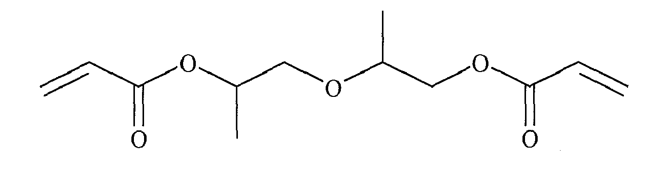
- (8) (A7) SR349. Ethoxylated(3) bisphenol A diacrylate, commercially available from Sartomer.

- (9) (A8) SR238. Hexanediol diacrylate, commercially available from Sartomer

- (10) (A9) Pentaerythritol triacrylate, commercially available from Aldrich

- The formulations were made by adding together the components shown in the Table 1 and stirring until the solid components were dissolved in the solvent mixture.
Table 1: Formulations for PMMA and PMMA/acrylate mixtures Product Formulation R1 (grams) Formulations F1-F9 (grams) MEK 16.60 16.60 MOP 8.30 8.30 Elvacite 2041 3.08 3.00 Benzophenone / 0.08 CN386 / 0.12 Darocur 1173 / 0.12 Acrylate Ax / 0.90 % solids 11.0 14.49 MEK = methylethyl ketone
MOP = 1-methoxy-2-propanol
CN386 = amine modified acrylate co-initiator,
commercially available from Sartomer
Darocur 1173 = photoinitiator,
commercially available from Ciba-Geigy
Acrylate Ax = acrylate A1 to A9 (see above structures). - The solutions were coated with a doctor blade at a wet thickness of 150 microns onto a powder phosphor screen. The coatings were then dried in a ventilated oven at 70ºC for 30 minutes, allowed to cool to room temperature and then passed three times under a Technigraf UL00855 UV lamp with a belt at a speed of 3m/min.
- The coatings were then treated with ethanol by rubbing the coatings 3x with a cotton pad soaked in ethanol. After allowing to dry and leaving overnight, the phosphor screens were bent round a metal cylinder with a diameter of 20mm, and then checked with a 20x magnifying glass for cracks.
- The powder phosphor screen was prepared as follows, before being coated with the covering protective layers as described above.
- Preparation of the photostimulable phosphor was performed as follows.
- Ba 0.859 Sr 0.14 Eu 0.01 F 2 was prepared by adiabatic reaction of the appropriate amounts of BaCO3, SrCO3 and Eu2O3 in an aqueous dispersion with HF.
- A raw mix was made by thoroughly mixing the following ingredients in the following proportions:
Ba0.859Sr0.14Eu0.01F2: 0.528 mole BaBr2: 0.375 mole BaI2: 0.095 mole NH4Br: 0.045 mole CsI: 0.003 mole PbF2: 0.0003 mole Sm2O3: 0.00025 mole Eu2O3: 0.00072 mole - The phosphor was made in 3 firing steps:
- Three crucibles, each containing 165 g of raw mix were placed in a quartz tube, which was sealed with a flange having a gas inlet and a gas outlet with water lock. After flushing with N2 for 15 minutes, the quartz tube was placed in a box furnace at 850°C. Dwell time in the furnace was 2 hours and the tube was flushed with N2 at 1.5 1/min.
- After that firing the tube was taken out of the furnace and left to cool for 30 minutes while being flushed with N2. Next, the crucibles were taken out of the tube and the powder was deagglomerated with mortar and pestle.
- The deagglomerated powder was milled on an Alpine AFG-100 air mill with three 3 mm nozzles, a milling chamber pressure of 3 bar and a wheel rotation rate of 3,500 r.p.m..
- Three crucibles containing 230 g of first fired material each, were placed in a quartz tube, which was sealed with a flange having a gas inlet and a gas outlet with water lock. The quartz tube was immediately placed in a box furnace at 725°C. Dwell time in the furnace was 5.5 hours and the tube was flushed with N2 at 1.5 1/min.
- After that firing the tube was allowed to cool in the furnace to 450°C while being flushed with N2. Next, the tube was opened, taken out of the furnace and allowed to cool further for 30'. The crucibles were taken out of the tube and the powder was deagglomerated with mortar and pestle.
- The deagglomerated powder was milled again on an Alpine AFG-100 air mill with three 3 mm nozzles, a milling chamber pressure of 3 bar and a wheel rotation rate of 3,500 r.p.m..
- Phosphors prepared in the above described way were used as starting material in order to prepare fine phosphor samples.
- The fine phosphors were made by remilling (3rd milling), refiring in the same way as in the second firing and remilling (4th milling) on the Alpine AFG-100 air-jet mill.
- 3rd and 4th milling rates were 9.000 rpm.
- The final fine particle size powder phosphor was seperately dispersed in a binder solution (see phosphor layer composition hereinafter).
Phosphor layer composition: STANN JF95B (from SANKYO ORGANIC Chemicals Co. Ltd.) 0.45 g KRATON FG19101X (from Shell Chemicals) 6.25 g BaSrFBr:Eu 150 g - STANN JF95B and KRATON FG19101X were dissolved while stirring in the prescribed amounts in 41.65 g of a solvent mixture from methylcyclohexane, toluene and butyl acetate in ratios by volume of 50:35:15. The phosphors were added thereafter and stirring was further proceeded for another 10 minutes at a rate of 1700 r.p.m.. Then the phosphor lacquer was given a ball-mill treatment during 1 min at 1700 r.p.m..
- The composition was doctor blade coated at a coating rate of 2.5 m per minute and a tickness of 600 □m onto a subbed 175 µm thick polyethylene terephthalate support and dried at room temperature during 30 minutes. In order to remove volatile solvents as much as possible the coated phosphor plate was dried at 60°C in a drying furnace.
- Results with respect to cracks in the topcoat layer are shown in Table 2.
Table 2 Formulation Acrylate type Cracks R1, comparison None Yes F1, invention CN435 No F2, invention SR344 No F3, invention SR610 No F4, comparison SR454 Yes (few) F5, comparison SR256 Yes F6, comparison SR508 Yes F7, comparison SR349 Yes (few) F8, comparison SR238 Yes F9, comparison Pentaerythritol triacrylate Yes (many) - As is clear from the data given in Table 2, coatings applied according to the present invention show the ability to be frequently cleaned, without being damaged by ethanol treatment and without showing cracks after bending. Moreover it has been established that a satisfactory scratch resistance was present.
- It can be seen from these results that only with cured topcoats from formulations having a (meth)acrylate type monomer with more than one (meth)acrylate group per monomer molecule and two or more ethyleneoxy groups per (meth)acrylate group in said monomer, the objectives of the present invention were attained.
- Having described in detail preferred embodiments of the current invention, it will now be apparent to those skilled in the art that numerous modifications can be made therein without departing from the scope of the invention as defined in the appending claims.
Claims (14)
- A photo- or electron beam curable composition comprising a polymer or copolymer and a (meth)acrylate type monomer with more than one (meth)acrylate group per monomer molecule and two or more ethylene oxy groups per (meth)acrylate group in said monomer.
- A photo- or electron beam curable composition according to claim 1, in which the polymer is polymethyl methacrylate or a copolymer thereof.
- A photo- or electron beam curable composition according to claim 1 or 2, wherein said composition is applied from a solvent mixture having less than 20 wt% of water.
- Photo-curable composition according to any one of the claims 1 to 3, wherein said composition further comprises a photo initiator.
- A layer-forming formulation in form of a solution, having a photo-or electron beam curable composition according to any one of the claims 1 to 4.
- Screen or panel comprising a support and a phosphor or scintillator layer thereupon, wherein said phosphor or scintillator layer is covered with the layer-forming formulation according to claim 5 in form of a dried layer.
- Screen or panel according to claim 6, wherein said dried layer has a thickness of at most 30 µm.
- Screen or panel according to claim 6 or 7, wherein said phosphor is a powder phosphor.
- Screen or panel according to claim 6 or 7, wherein said phosphor is a needle-shaped phosphor.
- Screen or panel according to claim 9, wherein said phosphor is a binderless phosphor.
- Screen or panel according to any one of the claims 6 to 10, wherein said phosphor is a photostimulable phosphor.
- Method of curing a layer-forming formulation according to claim 5, wherein curing proceeds by ultra-violet radiation or by electron beam curing.
- Method according to claim 12, wherein curing proceeds after coating said layer-forming formulation as a protective coating upon a phosphor layer or scintillator layer present on a support, followed by drying.
- Method according to claim 13, wherein said coating is performed by doctor blade coating or by bar coating.
Priority Applications (3)
| Application Number | Priority Date | Filing Date | Title |
|---|---|---|---|
| EP06118158A EP1884959B1 (en) | 2006-07-31 | 2006-07-31 | Phosphor or scintillator screens or panels having a topcoat layer. |
| US11/811,988 US20080026334A1 (en) | 2006-07-31 | 2007-06-13 | Topcoat layers for phosphor or scintillator screens or panels |
| JP2007180597A JP2008031474A (en) | 2006-07-31 | 2007-07-10 | Top coat layer for phosphor or scintillator screen or panel |
Applications Claiming Priority (1)
| Application Number | Priority Date | Filing Date | Title |
|---|---|---|---|
| EP06118158A EP1884959B1 (en) | 2006-07-31 | 2006-07-31 | Phosphor or scintillator screens or panels having a topcoat layer. |
Publications (2)
| Publication Number | Publication Date |
|---|---|
| EP1884959A1 true EP1884959A1 (en) | 2008-02-06 |
| EP1884959B1 EP1884959B1 (en) | 2011-09-14 |
Family
ID=37507856
Family Applications (1)
| Application Number | Title | Priority Date | Filing Date |
|---|---|---|---|
| EP06118158A Not-in-force EP1884959B1 (en) | 2006-07-31 | 2006-07-31 | Phosphor or scintillator screens or panels having a topcoat layer. |
Country Status (3)
| Country | Link |
|---|---|
| US (1) | US20080026334A1 (en) |
| EP (1) | EP1884959B1 (en) |
| JP (1) | JP2008031474A (en) |
Cited By (1)
| Publication number | Priority date | Publication date | Assignee | Title |
|---|---|---|---|---|
| WO2015144680A3 (en) * | 2014-03-27 | 2015-11-19 | Covestro Deutschland Ag | Coating agent and films having increased mechanical and chemical resistance and sufficient deformability in 2-d film insert molding methods |
Families Citing this family (6)
| Publication number | Priority date | Publication date | Assignee | Title |
|---|---|---|---|---|
| US20120018923A1 (en) * | 2010-07-20 | 2012-01-26 | Haochuan Jiang | System and method for forming a ceramic scintillator |
| DK2828345T3 (en) | 2012-03-22 | 2017-01-02 | 3M Innovative Properties Co | POLYMETHYLMETHACRYLATE-BASED HAIR COATING COMPOSITION AND COATED ARTICLE |
| WO2013145129A1 (en) * | 2012-03-27 | 2013-10-03 | 富士通株式会社 | Database management method, program and information processing device |
| US9581701B2 (en) * | 2014-12-16 | 2017-02-28 | Carestream Health, Inc. | Impact protection for wireless digital detector glass panel |
| US9939295B2 (en) | 2014-12-16 | 2018-04-10 | Carestream Health, Inc. | Impact protection for wireless digital detector glass panel |
| DE102018211874B4 (en) | 2018-07-17 | 2024-06-20 | Trumpf Laser Gmbh | Ring focus optics for peripheral welding of rotationally symmetrical workpieces |
Citations (9)
| Publication number | Priority date | Publication date | Assignee | Title |
|---|---|---|---|---|
| US4298650A (en) * | 1980-03-31 | 1981-11-03 | Eastman Kodak Company | Phosphorescent screens |
| JPS6337169A (en) * | 1986-07-31 | 1988-02-17 | Color Chem Kogyo Kk | Uv-curable binder composition |
| US4741993A (en) * | 1985-07-15 | 1988-05-03 | Konishiroku Photo Industry Co., Ltd. | Radiation image storage panel |
| US4893021A (en) * | 1987-01-27 | 1990-01-09 | Agfa-Gevaert, N.V. | Process for the production of multiple radiographic images |
| EP0510754A1 (en) * | 1991-04-26 | 1992-10-28 | Agfa-Gevaert N.V. | Luminescent article with protective coating and manufacture |
| EP0522609A1 (en) * | 1991-07-12 | 1993-01-13 | Agfa-Gevaert N.V. | Luminescent article used in radiography |
| US5432351A (en) * | 1992-10-26 | 1995-07-11 | Minnesota Mining And Manufacturing Company | X-ray intensifying screen |
| US6120902A (en) * | 1991-04-26 | 2000-09-19 | Van Havenbergh; Jan Emiel | Luminescent article with protective coating and manufacture |
| JP2001201851A (en) * | 2000-01-18 | 2001-07-27 | Asahi Kasei Corp | Photopolymerizable resin composition |
Family Cites Families (8)
| Publication number | Priority date | Publication date | Assignee | Title |
|---|---|---|---|---|
| US3859527A (en) * | 1973-01-02 | 1975-01-07 | Eastman Kodak Co | Apparatus and method for producing images corresponding to patterns of high energy radiation |
| JPH06236028A (en) * | 1993-02-08 | 1994-08-23 | Mitsubishi Rayon Co Ltd | Dry film resist |
| FR2711556B1 (en) * | 1993-10-29 | 1995-12-15 | Atohaas Holding Cv | A method of depositing a thin layer on the surface of a plastic substrate. |
| US6046269A (en) * | 1993-11-16 | 2000-04-04 | Warren J. Nass | Method for making a fresco-like finish from cement and a coating composition and the fresco-like finish made from the method |
| US5479430A (en) * | 1995-02-07 | 1995-12-26 | The Board Of Trustees Of The Leland Stanford Junior University | Protective coating for solid state slab lasers |
| US20040180226A1 (en) * | 2000-03-29 | 2004-09-16 | Subhankar Chatterjee | Radiation curable aqueous compositions for low extractable film packaging |
| JP4558178B2 (en) * | 2000-11-30 | 2010-10-06 | 新日鐵化学株式会社 | Light or thermosetting resin composition and printed wiring board |
| US20050260393A1 (en) * | 2004-05-24 | 2005-11-24 | Tsung-Neng Liao | Substrate capable of preventing from warping and having protective layers to prevent from scrubbing |
-
2006
- 2006-07-31 EP EP06118158A patent/EP1884959B1/en not_active Not-in-force
-
2007
- 2007-06-13 US US11/811,988 patent/US20080026334A1/en not_active Abandoned
- 2007-07-10 JP JP2007180597A patent/JP2008031474A/en active Pending
Patent Citations (9)
| Publication number | Priority date | Publication date | Assignee | Title |
|---|---|---|---|---|
| US4298650A (en) * | 1980-03-31 | 1981-11-03 | Eastman Kodak Company | Phosphorescent screens |
| US4741993A (en) * | 1985-07-15 | 1988-05-03 | Konishiroku Photo Industry Co., Ltd. | Radiation image storage panel |
| JPS6337169A (en) * | 1986-07-31 | 1988-02-17 | Color Chem Kogyo Kk | Uv-curable binder composition |
| US4893021A (en) * | 1987-01-27 | 1990-01-09 | Agfa-Gevaert, N.V. | Process for the production of multiple radiographic images |
| EP0510754A1 (en) * | 1991-04-26 | 1992-10-28 | Agfa-Gevaert N.V. | Luminescent article with protective coating and manufacture |
| US6120902A (en) * | 1991-04-26 | 2000-09-19 | Van Havenbergh; Jan Emiel | Luminescent article with protective coating and manufacture |
| EP0522609A1 (en) * | 1991-07-12 | 1993-01-13 | Agfa-Gevaert N.V. | Luminescent article used in radiography |
| US5432351A (en) * | 1992-10-26 | 1995-07-11 | Minnesota Mining And Manufacturing Company | X-ray intensifying screen |
| JP2001201851A (en) * | 2000-01-18 | 2001-07-27 | Asahi Kasei Corp | Photopolymerizable resin composition |
Non-Patent Citations (2)
| Title |
|---|
| DATABASE WPI Section Ch Week 198813, Derwent World Patents Index; Class A11, AN 1988-087274, XP002394751 * |
| DATABASE WPI Section Ch Week 200217, Derwent World Patents Index; Class A12, AN 2002-125526, XP002394752 * |
Cited By (2)
| Publication number | Priority date | Publication date | Assignee | Title |
|---|---|---|---|---|
| WO2015144680A3 (en) * | 2014-03-27 | 2015-11-19 | Covestro Deutschland Ag | Coating agent and films having increased mechanical and chemical resistance and sufficient deformability in 2-d film insert molding methods |
| US10344170B2 (en) | 2014-03-27 | 2019-07-09 | Covestro Deutschland Ag | Coating agent and films having increased mechanical and chemical resistance and sufficient deformability in 2-D film insert molding methods |
Also Published As
| Publication number | Publication date |
|---|---|
| EP1884959B1 (en) | 2011-09-14 |
| JP2008031474A (en) | 2008-02-14 |
| US20080026334A1 (en) | 2008-01-31 |
Similar Documents
| Publication | Publication Date | Title |
|---|---|---|
| US20080026334A1 (en) | Topcoat layers for phosphor or scintillator screens or panels | |
| JP3827298B2 (en) | Manufacturing method of radiation image conversion panel | |
| US6707050B2 (en) | Radiation image storage panel | |
| US20080035857A1 (en) | Method of manufacturing a radiation image storage panel | |
| JP3743561B2 (en) | Radiation image conversion panel | |
| US20030168611A1 (en) | Binderless storage phosphor screen on a dedicate suport | |
| US20080026155A1 (en) | Polymer compositions and use thereof as topcoat layers for phosphor or scintillator screens or panels | |
| US20070246660A1 (en) | Radiation image phosphor or scintillator panel | |
| JP2002098799A (en) | Radiation luminescent panel | |
| EP1892729A1 (en) | Method of manufacturing a radiation image storage panel | |
| JP2004037363A (en) | Method for manufacturing radiation image conversion panel | |
| JP2005091200A (en) | Radiological image conversion panel, its manufacturing method, and radiation detection instrument using it | |
| JP2003028996A (en) | Manufacturing method for radiation image conversion panel | |
| EP1347460A1 (en) | A binderless storage phosphor screen having voids partially filled | |
| JPH1184096A (en) | Amplifier screen for x-ray photographing and its production method | |
| JP4411810B2 (en) | Manufacturing method of radiation image conversion panel | |
| JP2004212245A (en) | Method of manufacturing radiation image conversion panel | |
| EP1998338A1 (en) | Needle image plate or panel suitable for use in CR or DR imaging. | |
| JP2003302498A (en) | Manufacturing method of radiological image conversion panel | |
| JP2002098800A (en) | Radiation luminescent panel | |
| JP2004170405A (en) | Method of manufacturing radiological image converting panel | |
| JP2004191062A (en) | Manufacturing method of radiological image conversion panel | |
| JP2002022895A (en) | Radiation image conversion panel | |
| JP2001324600A (en) | Radiation image converting panel | |
| JP2002107496A (en) | Panel for converting radiation image, and manufacturing method therefor |
Legal Events
| Date | Code | Title | Description |
|---|---|---|---|
| PUAI | Public reference made under article 153(3) epc to a published international application that has entered the european phase |
Free format text: ORIGINAL CODE: 0009012 |
|
| AK | Designated contracting states |
Kind code of ref document: A1 Designated state(s): AT BE BG CH CY CZ DE DK EE ES FI FR GB GR HU IE IS IT LI LT LU LV MC NL PL PT RO SE SI SK TR |
|
| AX | Request for extension of the european patent |
Extension state: AL BA HR MK YU |
|
| RAP1 | Party data changed (applicant data changed or rights of an application transferred) |
Owner name: AGFA HEALTHCARE NV |
|
| 17P | Request for examination filed |
Effective date: 20080806 |
|
| AKX | Designation fees paid |
Designated state(s): DE FR GB |
|
| 17Q | First examination report despatched |
Effective date: 20100608 |
|
| GRAP | Despatch of communication of intention to grant a patent |
Free format text: ORIGINAL CODE: EPIDOSNIGR1 |
|
| RTI1 | Title (correction) |
Free format text: PHOSPHOR OR SCINTILLATOR SCREENS OR PANELS HAVING A TOPCOAT LAYER. |
|
| GRAS | Grant fee paid |
Free format text: ORIGINAL CODE: EPIDOSNIGR3 |
|
| GRAA | (expected) grant |
Free format text: ORIGINAL CODE: 0009210 |
|
| AK | Designated contracting states |
Kind code of ref document: B1 Designated state(s): DE FR GB |
|
| REG | Reference to a national code |
Ref country code: DE Ref legal event code: R096 Ref document number: 602006024345 Country of ref document: DE Effective date: 20111208 |
|
| PLBE | No opposition filed within time limit |
Free format text: ORIGINAL CODE: 0009261 |
|
| STAA | Information on the status of an ep patent application or granted ep patent |
Free format text: STATUS: NO OPPOSITION FILED WITHIN TIME LIMIT |
|
| 26N | No opposition filed |
Effective date: 20120615 |
|
| REG | Reference to a national code |
Ref country code: DE Ref legal event code: R097 Ref document number: 602006024345 Country of ref document: DE Effective date: 20120615 |
|
| PGFP | Annual fee paid to national office [announced via postgrant information from national office to epo] |
Ref country code: FR Payment date: 20130703 Year of fee payment: 8 |
|
| PGFP | Annual fee paid to national office [announced via postgrant information from national office to epo] |
Ref country code: DE Payment date: 20130612 Year of fee payment: 8 |
|
| PGFP | Annual fee paid to national office [announced via postgrant information from national office to epo] |
Ref country code: GB Payment date: 20130703 Year of fee payment: 8 |
|
| REG | Reference to a national code |
Ref country code: DE Ref legal event code: R119 Ref document number: 602006024345 Country of ref document: DE |
|
| GBPC | Gb: european patent ceased through non-payment of renewal fee |
Effective date: 20140731 |
|
| REG | Reference to a national code |
Ref country code: FR Ref legal event code: ST Effective date: 20150331 |
|
| PG25 | Lapsed in a contracting state [announced via postgrant information from national office to epo] |
Ref country code: DE Free format text: LAPSE BECAUSE OF NON-PAYMENT OF DUE FEES Effective date: 20150203 |
|
| REG | Reference to a national code |
Ref country code: DE Ref legal event code: R119 Ref document number: 602006024345 Country of ref document: DE Effective date: 20150203 |
|
| PG25 | Lapsed in a contracting state [announced via postgrant information from national office to epo] |
Ref country code: FR Free format text: LAPSE BECAUSE OF NON-PAYMENT OF DUE FEES Effective date: 20140731 Ref country code: GB Free format text: LAPSE BECAUSE OF NON-PAYMENT OF DUE FEES Effective date: 20140731 |