EP1873565A2 - Demodulation eines Signals mittels eines 1-x-m-Kopplers - Google Patents
Demodulation eines Signals mittels eines 1-x-m-Kopplers Download PDFInfo
- Publication number
- EP1873565A2 EP1873565A2 EP07012371A EP07012371A EP1873565A2 EP 1873565 A2 EP1873565 A2 EP 1873565A2 EP 07012371 A EP07012371 A EP 07012371A EP 07012371 A EP07012371 A EP 07012371A EP 1873565 A2 EP1873565 A2 EP 1873565A2
- Authority
- EP
- European Patent Office
- Prior art keywords
- signal
- phase
- operable
- pair
- optical
- Prior art date
- Legal status (The legal status is an assumption and is not a legal conclusion. Google has not performed a legal analysis and makes no representation as to the accuracy of the status listed.)
- Withdrawn
Links
Images


Classifications
-
- H—ELECTRICITY
- H04—ELECTRIC COMMUNICATION TECHNIQUE
- H04B—TRANSMISSION
- H04B10/00—Transmission systems employing electromagnetic waves other than radio-waves, e.g. infrared, visible or ultraviolet light, or employing corpuscular radiation, e.g. quantum communication
- H04B10/60—Receivers
- H04B10/66—Non-coherent receivers, e.g. using direct detection
- H04B10/67—Optical arrangements in the receiver
- H04B10/676—Optical arrangements in the receiver for all-optical demodulation of the input optical signal
- H04B10/677—Optical arrangements in the receiver for all-optical demodulation of the input optical signal for differentially modulated signal, e.g. DPSK signals
Definitions
- This invention relates generally to the field of signal communication and more specifically to demodulating a signal using a 1 x m coupler.
- Signals may be modulated according to a differential phase-shifted keying (DPSK) digital modulation technique.
- DPSK differential phase-shifted keying
- changes in phase are used to represent bit data.
- a modulator at a transmitter translates an input bit sequence into phase changes that represent the input bit sequence.
- a demodulator at a receiver translates the phase changes to retrieve the input bit sequence.
- a demodulator includes a 1 x m optical coupler and one or more optical device sets.
- the 1 x m optical coupler splits an input signal comprising symbols to yield m signals comprising m/2 pairs of signals.
- An optical device set is associated with a pair of signals and includes one or more first optical operators, one or more second optical operators, and a set coupler.
- the first optical operators direct a first signal of a pair of signals along a first path
- the second optical operators direct a second signal of the pair along a second path.
- the second path introduces a symbol delay between the first signal and the second signal.
- the set coupler receives the first and the second signal to generate interference.
- the interference indicates a phase shift between a phase corresponding to a symbol and a successive phase corresponding to a successive symbol.
- a technical advantage of one embodiment may be that a demodulator includes a 1 x m coupler operable to split a signal into m signals. Use of the 1 x m coupler instead of successive 1 x 2 couplers may reduce the complexity of the demodulator.
- FIGURES 1 through 4 of the drawings like numerals being used for like and corresponding parts of the various drawings.
- FIGURE 1 is a block diagram illustrating one embodiment of a system 10 for communicating a signal according to a differential phase-shifted keying (DPSK) modulation technique.
- system 10 includes a demodulator that includes a 1 x m coupler operable to split a signal into m signals. Use of the 1 x m coupler instead of successive 1 x 2 couplers may reduce the complexity of the demodulator.
- system 10 communicates signals.
- a signal may refer to an optical signal transmitted as light pulses comprising photons.
- An optical signal may have a wavelength of approximately 1550 nanometers, and a data rate of, for example, 10, 20, 40, or over 40 gigabits per second.
- a signal may communicate information in packets.
- a packet may comprise a bundle of data organized in a specific way for transmission.
- a packet may carry any suitable information such as voice, data, audio, video, multimedia, other information, or any combination of the preceding.
- System 10 includes components that include any suitable arrangement of elements operable to perform the operations of the component, and may comprise logic, an interface, a memory, or any suitable combination of the preceding.
- Logic may refer to hardware, software, other logic, or any suitable combination of the preceding. Certain logic may manage the operation of a device, and may comprise, for example, a processor.
- Processor may refer to any suitable device operable to execute instructions and manipulate data to perform operations.
- Interface may refer to logic of a device operable to receive input for the device, send output from the device, perform suitable processing of the input or output or both, or any combination of the preceding, and may comprise one or more ports, conversion software, or both.
- Memory may refer to logic operable to store and facilitate retrieval of information, and may comprise Random Access Memory (RAM), Read Only Memory (ROM), a magnetic drive, a disk drive, a Compact Disk (CD) drive, a Digital Video Disk (DVD) drive, removable media storage, any other suitable data storage medium, or a combination of any of the preceding.
- RAM Random Access Memory
- ROM Read Only Memory
- CD Compact Disk
- DVD Digital Video Disk
- system 10 includes a transmitter 20 operable to communicate a signal to a receiver 32.
- Transmitter 20 includes a modulator 24 that encodes the signal according to DPSK modulation.
- Receiver 32 includes a demodulator 28 that decodes the encoded signal.
- modulator 24 receives a signal with input bits b k for time slots k. Modulator 24 encodes bits b k to yield modulated signal m k .
- Modulator 24 may comprise any suitable modulator, for example, a Mach-Zehner modulator. Modulator 24 may have a laser that emits a continuous wave light beam, and may modulate the light beam to encodes bits b k .
- Bits b k may be encoded according to DPSK modulation where phase shifts between successive symbols represent bits b k .
- 4-PSK, or differential quadrature phase-shifted keying (DQPSK) four phase differences are used to encode two bits per symbol.
- phase shifts 0°, 90°, 180°, and -90° may be used to encode "00", "01", "11", and "10", respectively.
- 8-PSK eight phase differences are used to encode three bits per symbol.
- Transmitter 20 transmits modulated signal m k to receiver 32.
- Demodulator 28 of receiver 32 demodulates signal m k to reverse the encoding procedure to yield bits b k .
- demodulator 28 compares the phase shifts between successive symbols.
- Demodulator 28 may split signal m k to yield multiple signals. A signal of the multiple signals may be delayed by one symbol to yield a delayed signal. The delayed signal and a nondelayed signal may be overlapped to compare the phases of successive symbols. The phases may be compared by constructively and destructively interfering the overlapped signals.
- Demodulator 28 may include photodiodes that detect the interference and generate a detector signal representing the interference.
- demodulator 28 includes a 1 x m coupler operable to split a signal into m signals. Use of the 1 x m coupler instead of successive 1 x 2 couplers may reduce the complexity of demodulator 28.
- An example of demodulator 28 is described in more detail with reference to FIGURE 2.
- system 10 may be integrated or separated according to particular needs. Moreover, the operations of system 10 may be performed by more, fewer, or other devices. Additionally, operations of system 10 may be performed using any suitable logic. As used in this document, "each" refers to each member of a set or each member of a subset of a set.
- FIGURE 2 is a diagram illustrating one embodiment of a demodulator 28 that includes a 1 x m coupler operable to split a signal into m signals. Use of the 1 x m coupler instead of successive 1 x 2 couplers may reduce the complexity of demodulator 28.
- demodulator 28 includes an input 120, a 1 x m coupler 124, a plurality of phase delays 126, a plurality of couplers 128, and a plurality of optical to electric converter(o/e converter) 132 coupled by waveguides 136 as shown.
- the o/e converter 132 includes photodiodes.
- Input 120 is operable to receive an input signal.
- Coupler 124 is operable to split a signal into m signals, or m/2 pairs 140 of signals, and may be embodied in a single optical device.
- An optical device set 138 may receive a pair 140 of signals.
- An optical device set 138 may comprise optical operators operable to communicate, filter, split, reflect, or otherwise process a signal.
- an optical device set 138 comprises waveguides 136.
- a pair 140 of signals travels along paths 144 and 148 of an optical device set 138 to a coupler 128.
- the difference in the lengths of paths 144 and 148 introduces a relative symbol delay between the signals.
- the difference may be one symbol length, which may be established from the ratio of the group velocity and the symbol rate.
- the symbol delay allows for comparison of the phases corresponding to successive symbols.
- a phase delay 126 of path 144 delays the phase of the signal along path 144.
- the phase may be delayed to allow for comparison of the phases corresponding to successive symbols.
- a thin-film heater may be used to adjust the delays.
- Coupler 128 combines the signals from paths 144 and 148.
- o/e converter 132 including photodiodes detect constructive and destructive interference of the combined signals.
- demodulator 28 may be made to demodulator 28 without departing from the scope of the invention.
- the components of demodulator 28 may be integrated or separated according to particular needs.
- the operations of demodulator 28 may be performed by more, fewer, or other devices.
- demodulator 28 may have fewer components than a demodulator that has a coupler for each pair 140 of signals. Accordingly, demodulator 28 may have reduced insertion loss and reduced complexity.
- FIGURE 3 is a block diagram illustrating one example of a demodulator 28 that may be used for 4-PSK demodulation.
- demodulator 28 includes input 120, a 1 x 4 coupler 124, phase delays 126a-b, couplers 128a-b, and o/e converter 132a-b coupled by waveguides 136 as shown.
- the o/e converter 132a-b includes photodiodes.
- Phase delay 126a comprises a - ⁇ /4 phase delay
- phase delay 126b comprises a +n/4 phase delay.
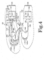
- FIGURE 4 is a block diagram illustrating one example of a demodulator 28 that may be used for 8-PSK demodulation.
- demodulator 28 includes input 120, a 1 x 6 coupler 124, phase delays 126a-c, couplers 128a-c, and o/e converter 132a-c coupled by waveguides 136 as shown.
- the o/e converter 132a-c includes photodiodes.
- Phase delay 126a comprises a +15 ⁇ /8 phase delay
- phase delay 126b comprises a +7 ⁇ /4 phase delay
- phase delay 126c comprises a +n/4 phase delay.
- a technical advantage of one embodiment may be that a demodulator includes a 1 x m coupler operable to split a signal into m signals. Use of the 1 x m coupler instead of successive 1 x 2 couplers may reduce the complexity of the demodulator.
Landscapes
- Physics & Mathematics (AREA)
- Electromagnetism (AREA)
- Engineering & Computer Science (AREA)
- Computer Networks & Wireless Communication (AREA)
- Signal Processing (AREA)
- Optical Communication System (AREA)
- Optical Modulation, Optical Deflection, Nonlinear Optics, Optical Demodulation, Optical Logic Elements (AREA)
Applications Claiming Priority (1)
| Application Number | Priority Date | Filing Date | Title |
|---|---|---|---|
| US11/479,826 US20080002994A1 (en) | 2006-06-30 | 2006-06-30 | Demodulating a signal using a 1 x m coupler |
Publications (1)
| Publication Number | Publication Date |
|---|---|
| EP1873565A2 true EP1873565A2 (de) | 2008-01-02 |
Family
ID=38659656
Family Applications (1)
| Application Number | Title | Priority Date | Filing Date |
|---|---|---|---|
| EP07012371A Withdrawn EP1873565A2 (de) | 2006-06-30 | 2007-06-25 | Demodulation eines Signals mittels eines 1-x-m-Kopplers |
Country Status (3)
| Country | Link |
|---|---|
| US (1) | US20080002994A1 (de) |
| EP (1) | EP1873565A2 (de) |
| JP (1) | JP2008017443A (de) |
Families Citing this family (2)
| Publication number | Priority date | Publication date | Assignee | Title |
|---|---|---|---|---|
| JP2011250126A (ja) * | 2010-05-26 | 2011-12-08 | Sumitomo Electric Ind Ltd | トランスインピーダンスアンプ及び光レシーバ |
| US20180242811A1 (en) * | 2017-02-24 | 2018-08-30 | Kirk Staresinic | Grill cleaning device and method |
Family Cites Families (4)
| Publication number | Priority date | Publication date | Assignee | Title |
|---|---|---|---|---|
| US6626589B1 (en) * | 1999-12-29 | 2003-09-30 | Nortel Networks Limited | Optical packet switching |
| GB2385144B (en) * | 2002-01-23 | 2006-02-08 | Marconi Optical Components Ltd | Optical signal demodulators |
| US7343104B2 (en) * | 2004-06-23 | 2008-03-11 | Lucent Technologies Inc. | Apparatus and method for receiving a quadrature differential phase shift key modulated optical pulsetrain |
| JP4710387B2 (ja) * | 2005-04-06 | 2011-06-29 | 富士通株式会社 | 差分m位相偏移変調方式に対応した光受信器および光受信方法 |
-
2006
- 2006-06-30 US US11/479,826 patent/US20080002994A1/en not_active Abandoned
-
2007
- 2007-03-27 JP JP2007082223A patent/JP2008017443A/ja not_active Withdrawn
- 2007-06-25 EP EP07012371A patent/EP1873565A2/de not_active Withdrawn
Also Published As
| Publication number | Publication date |
|---|---|
| US20080002994A1 (en) | 2008-01-03 |
| JP2008017443A (ja) | 2008-01-24 |
Similar Documents
| Publication | Publication Date | Title |
|---|---|---|
| US8218975B2 (en) | Free-space DQPSK demodulator | |
| US9621274B2 (en) | Optical communication system | |
| CN101860500B (zh) | 一种产生、接收相位偏振调制信号的方法、装置和系统 | |
| US8369442B2 (en) | Communicating a signal according to ASK modulation and PSK modulation | |
| US8437644B2 (en) | Vestigial phase shift keying modulation and systems and methods incorporating same | |
| US7912378B2 (en) | Modulating a signal using a fractional phase modulator | |
| US20080170862A1 (en) | Monitoring Polarization Of A Signal Communicated According To Polarization Multiplexing | |
| JP4441275B2 (ja) | ダイレクト光学n相位相シフトキーイングを用いたエンコーダ、そのシステム及びエンコード方法 | |
| US20040141222A1 (en) | Optical phase multi-level modulation method and apparatus, and error control method | |
| US7778360B2 (en) | Demodulating a signal encoded according to ASK modulation and PSK modulation | |
| WO2007001090A1 (ja) | Dpsk変復調方法、これを用いた光通信装置および光通信システム | |
| US7860402B2 (en) | Modulating a signal according to 2n-PSK modulation | |
| EP1909445A2 (de) | Erfassung von Fehlanpassungen in einem PSK-Empfänger | |
| EP1873565A2 (de) | Demodulation eines Signals mittels eines 1-x-m-Kopplers | |
| US7941058B2 (en) | Device and method for decoding an optical multi-level DPSK signal | |
| US10256907B2 (en) | System and method for coherent detection with digital signal procession | |
| US7650083B2 (en) | Demodulating a signal by performing consecutive beam splitting | |
| JP2003198463A (ja) | 共通クロックを備えた光ファイバー伝送システム | |
| JP2012156749A (ja) | 光受信器 | |
| JP4842224B2 (ja) | ディジタル伝送システム | |
| JP2003046446A (ja) | 光信号処理回路 | |
| JP2007181036A (ja) | 光位相多値変調方式、光通信装置、光送信器および光受信器 |
Legal Events
| Date | Code | Title | Description |
|---|---|---|---|
| PUAI | Public reference made under article 153(3) epc to a published international application that has entered the european phase |
Free format text: ORIGINAL CODE: 0009012 |
|
| AK | Designated contracting states |
Kind code of ref document: A2 Designated state(s): AT BE BG CH CY CZ DE DK EE ES FI FR GB GR HU IE IS IT LI LT LU LV MC MT NL PL PT RO SE SI SK TR |
|
| AX | Request for extension of the european patent |
Extension state: AL BA HR MK YU |
|
| STAA | Information on the status of an ep patent application or granted ep patent |
Free format text: STATUS: THE APPLICATION HAS BEEN WITHDRAWN |
|
| 18W | Application withdrawn |
Effective date: 20091012 |