EP1869499B1 - Schaltkreis zur detektion von teilchen mit einzel-schaltkreisen, die unter-pixel darstellen - Google Patents
Schaltkreis zur detektion von teilchen mit einzel-schaltkreisen, die unter-pixel darstellen Download PDFInfo
- Publication number
- EP1869499B1 EP1869499B1 EP05815036.8A EP05815036A EP1869499B1 EP 1869499 B1 EP1869499 B1 EP 1869499B1 EP 05815036 A EP05815036 A EP 05815036A EP 1869499 B1 EP1869499 B1 EP 1869499B1
- Authority
- EP
- European Patent Office
- Prior art keywords
- pixel
- circuit
- input
- circuits
- output
- Prior art date
- Legal status (The legal status is an assumption and is not a legal conclusion. Google has not performed a legal analysis and makes no representation as to the accuracy of the status listed.)
- Ceased
Links
- 238000001514 detection method Methods 0.000 title claims description 46
- 239000002245 particle Substances 0.000 claims description 49
- 239000000872 buffer Substances 0.000 claims description 13
- 239000011159 matrix material Substances 0.000 claims description 10
- 230000004907 flux Effects 0.000 description 10
- 230000006870 function Effects 0.000 description 5
- 238000011144 upstream manufacturing Methods 0.000 description 5
- 206010033799 Paralysis Diseases 0.000 description 4
- 239000000969 carrier Substances 0.000 description 2
- 230000001769 paralizing effect Effects 0.000 description 2
- 230000004913 activation Effects 0.000 description 1
- 230000006399 behavior Effects 0.000 description 1
- 230000007423 decrease Effects 0.000 description 1
- 238000002059 diagnostic imaging Methods 0.000 description 1
- 235000021183 entrée Nutrition 0.000 description 1
- 238000003384 imaging method Methods 0.000 description 1
- 230000002401 inhibitory effect Effects 0.000 description 1
- 230000005764 inhibitory process Effects 0.000 description 1
- 230000010354 integration Effects 0.000 description 1
- 238000004519 manufacturing process Methods 0.000 description 1
- 238000002601 radiography Methods 0.000 description 1
- 230000009467 reduction Effects 0.000 description 1
- 230000002123 temporal effect Effects 0.000 description 1
- 230000001131 transforming effect Effects 0.000 description 1
Images


Classifications
-
- G—PHYSICS
- G01—MEASURING; TESTING
- G01T—MEASUREMENT OF NUCLEAR OR X-RADIATION
- G01T1/00—Measuring X-radiation, gamma radiation, corpuscular radiation, or cosmic radiation
- G01T1/16—Measuring radiation intensity
- G01T1/24—Measuring radiation intensity with semiconductor detectors
-
- G—PHYSICS
- G01—MEASURING; TESTING
- G01T—MEASUREMENT OF NUCLEAR OR X-RADIATION
- G01T1/00—Measuring X-radiation, gamma radiation, corpuscular radiation, or cosmic radiation
- G01T1/29—Measurement performed on radiation beams, e.g. position or section of the beam; Measurement of spatial distribution of radiation
-
- G—PHYSICS
- G01—MEASURING; TESTING
- G01T—MEASUREMENT OF NUCLEAR OR X-RADIATION
- G01T1/00—Measuring X-radiation, gamma radiation, corpuscular radiation, or cosmic radiation
- G01T1/29—Measurement performed on radiation beams, e.g. position or section of the beam; Measurement of spatial distribution of radiation
- G01T1/2914—Measurement of spatial distribution of radiation
- G01T1/2921—Static instruments for imaging the distribution of radioactivity in one or two dimensions; Radio-isotope cameras
- G01T1/2928—Static instruments for imaging the distribution of radioactivity in one or two dimensions; Radio-isotope cameras using solid state detectors
-
- H—ELECTRICITY
- H04—ELECTRIC COMMUNICATION TECHNIQUE
- H04N—PICTORIAL COMMUNICATION, e.g. TELEVISION
- H04N25/00—Circuitry of solid-state image sensors [SSIS]; Control thereof
- H04N25/70—SSIS architectures; Circuits associated therewith
- H04N25/76—Addressed sensors, e.g. MOS or CMOS sensors
- H04N25/77—Pixel circuitry, e.g. memories, A/D converters, pixel amplifiers, shared circuits or shared components
- H04N25/772—Pixel circuitry, e.g. memories, A/D converters, pixel amplifiers, shared circuits or shared components comprising A/D, V/T, V/F, I/T or I/F converters
-
- H—ELECTRICITY
- H04—ELECTRIC COMMUNICATION TECHNIQUE
- H04N—PICTORIAL COMMUNICATION, e.g. TELEVISION
- H04N25/00—Circuitry of solid-state image sensors [SSIS]; Control thereof
- H04N25/70—SSIS architectures; Circuits associated therewith
- H04N25/76—Addressed sensors, e.g. MOS or CMOS sensors
- H04N25/77—Pixel circuitry, e.g. memories, A/D converters, pixel amplifiers, shared circuits or shared components
- H04N25/772—Pixel circuitry, e.g. memories, A/D converters, pixel amplifiers, shared circuits or shared components comprising A/D, V/T, V/F, I/T or I/F converters
- H04N25/773—Pixel circuitry, e.g. memories, A/D converters, pixel amplifiers, shared circuits or shared components comprising A/D, V/T, V/F, I/T or I/F converters comprising photon counting circuits, e.g. single photon detection [SPD] or single photon avalanche diodes [SPAD]
Definitions
- the invention relates to a particle detection circuit comprising a plurality of elementary circuits, each comprising a particle detector element connected to associated counting means delivering counting signals representative of the number of particles detected by the corresponding detector element.
- Imaging devices particularly in the field of radiology (radiography, radioscopy) use particle detection circuits (X or gamma photons) comprising elementary circuits arranged in the form of matrix of rows and columns and each corresponding to a pixel.
- X particle detection circuits
- Some operate by integration of electric charges and their dynamics are limited, downwards, by the thermal noise (typically of the order of 100 ⁇ V in rms value) and, upwards, by the supply voltage (for example from order of 1 V).
- Others operate by counting events and are therefore limited by the characteristics of the meter, including its capacity.
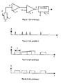
- a conventional detection circuit comprises a detector element 1, transforming the p- detected particles into electrical pulses.
- the output of the detector element 1 is connected, generally via a low-noise preamplifier 2, to an input of a comparator 3, another input of which is connected to a Threshold voltage Vs.
- Comparator 3 thus provides a binary signal at the count input of a counter 4 whenever the detection of a particle produces a pulse of sufficient amplitude.
- the counter 4 thus provides binary signals representative of the number of particles detected by the detector element 1.
- the counter 4 comprises a reset input R.
- the spatial resolution of the circuit is defined by the pixel, which corresponds to an elementary point of the matrix and the image.
- the Figures 2 to 4 illustrate the temporal behavior of detection circuits according to the prior art.
- the output pulses A of the detector element of the detection circuit according to the figure 1 each pulse corresponding to the detection of an incident particle.
- the entire processing chain from the detector to the meter, requires a processing time ⁇ , related to the transit time of the carriers in the detector element 1 and to the processing time of the electronic circuits, conventionally called service time or time death, during which the system is not available.
- the dead time ⁇ is negligible with regard to the particle flow ⁇ , that is to say, when ⁇ ⁇ 1 / ⁇ , the detection circuit correctly detects all the particles.
- the rate counting corresponding to the number of incident particles actually counted by the counter 4 decreases to paralyze the system, as shown in FIG. figure 3 , which represents the signals B at the output of the comparator 3 of a detection circuit according to the figure 1 of a paralytic system. Indeed, if a particle is detected by the detector element 1 during the processing time of the detection of the previous particle, the detection circuit ignores the last detected particle. There is then stacking. This phenomenon is earlier in a paralyzable system ( figure 3 ) in a non-paralyzed system ( figure 4 ).
- the number m of particles counted is a function of the number n of incident particles and the dead time ⁇ introduced by the circuit.
- m ne -n ⁇
- m n / (1 + n ⁇ )
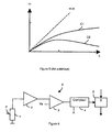
- the figure 5 illustrates the variations in the number m of particles counted as a function of the flux ⁇ of incident particles detected by the detector element 1, respectively in a non-paralyzed system (curve C1) and in a paralyzable system (curve C2).
- the document EP-A-1424568 discloses a particle detector with a standard spatial resolution for a medium to strong particle flux and a pixel cluster, using OR logic gates arranged upstream of the counters associated with the detector elements, to increase the signal-to-noise ratio in the case of weak streams (noisy image).
- the detector In the first case, the detector is sensitive to the stack of events and in the second case, the spatial resolution is degraded. In all cases, the dead time is unchanged and the detector does not work properly when the particle flow is very high.
- the object of the invention is to overcome the disadvantages of known detection circuits and, more particularly, to enable the detection of high particle fluxes with a good spatial resolution.
- each elementary circuit comprises a summing circuit having first and second inputs and an output, the first input of the summation circuit of an elementary circuit being connected to the output of the means.
- Associated counting a predetermined number of elementary circuits constituting a pixel in which the summation circuits are connected in series, between an input of the pixel constituted by the second input of the summation circuit of a first elementary circuit of the pixel, and an output of the pixel, constituted by the output of the summation circuit of a last elementary circuit of the pixel and providing counting signals representative of the number of particles detected by all the elementary circuits of the pixel.
- each elementary circuit includes selective zeroing means of the first input of the corresponding summation circuit.
- each elementary circuit E of a detection circuit comprises at least one detector element 1 and a counter 4, preferably connected, as in FIG. figure 1 , via a preamplifier 2 and a comparator 3, and a summing circuit 5, comprising first and second inputs and an output.
- the counting signals supplied at the output of the counter 4 and representative of the number of particles p detected by the detector element corresponding 1, are applied to the first input of the corresponding summation circuit 5.
- a detection circuit comprises a plurality of elementary circuits E constituting a pixel in which the summation circuits are connected in series between an input of the pixel constituted by the second input of the summation circuit 5 of a first elementary circuit of the pixel, and an output of the pixel constituted by the output of the summation circuit of a last elementary circuit of the pixel.
- the second input of the first elementary circuit of a pixel is connected to zero, while the second input of the summation circuit 5 of each of the other elementary circuits of the pixel is connected to the output of the summation circuit 5 of the previous elementary circuit.
- the output of the summation circuit of the last elementary circuit of the pixel then constitutes the output of the pixel and provides count signals representative of the number of incident particles detected by all the elementary circuits E of the pixel.
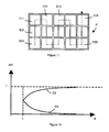
- 16 elementary circuits form a matrix of 4 rows and 4 columns, each elementary circuit Eij being identified by its line indices i and column j.
- the first elementary circuit of the pixel is the elementary circuit E32.
- the output of its summing circuit 5 is connected to the second input of the summation circuit 5 of the last elementary circuit E44 of the pixel by means of summation circuits, connected in series, of the elementary circuits E22, E23, E33, E43, E42, E41, E31, E21, E11, E12, E13, E14, E24 and E34, thereby forming a spiral path, which passes only once each elementary circuit E.
- the second input of the summation circuit of the elementary circuit E32 is connected to zero.
- the first elementary circuit of the pixel is the elementary circuit E41.
- the output of its summation circuit 5 is connected to the second input of the summation circuit 5 of the last elementary circuit E44 of the pixel by means of summation circuits, connected in series, of the elementary circuits E31, E21, E11, E12, E22, E32, E42, E43, E33, E23, E13, E14, E24 and E34, thus forming another path which crosses only once each elementary circuit E.
- the second input of the summation circuit of the elementary circuit E41 is connected to zero.
- the path may be any, provided to pass once by each of the elementary circuits of the pixel.
- This cascading structure makes it possible to browse all the elementary circuits, which form sub-pixels, and to add the contents of all the counters.
- the sum of the content of all the counters is thus obtained, representative of the number of incident particles detected by the set of detector elements 1 of all the elementary circuits considered.
- the set of elementary circuits thus connected defines a pixel, that is to say a point of the detection circuit that provides point count information, which can be transferred by a bus and used to form a final image.
- the size of each pixel defines the spatial resolution of the detection circuit and therefore of the final image. To achieve a high spatial resolution, the pixels are small and the electronic detection circuit can then be realized by a specific integrated circuit (ASIC).
- ASIC application specific integrated circuit
- Figures 7 and 8 ).
- the flux ⁇ of particles reaching the pixel is divided by K at each sub-pixel, that is to say at the level of each elementary circuit E, where it is reduced to ⁇ / K.
- the dead time ⁇ related to the transit time of the carriers in the detector element 1 and to the processing time of the electronic circuits, is to be compared with K / ⁇ and no longer at 1 / ⁇ .
- the dead time ⁇ is therefore all the more easily negligible as the number K of elementary cells constituting a pixel is large. Indeed, it is then easier to check the inequality ⁇ ⁇ K / ⁇ . In practice, everything happens as if the dead time ⁇ of a pixel which would have included only one counting chain had been divided by K. This makes it possible to considerably delay the phenomenon of stacking described above with regard to of the Figures 3 and 4 .
- the resolution of the detection circuit is therefore no longer limited by the flow of particles to be managed.
- the division of the pixels into subpixels and, consequently, the reduction in the size of the elementary circuits, which constitute subpixels and not pixels, make it possible, for the same spatial resolution, to artificially reduce the quantity of pulses to be managed. for a given time by each elementary circuit.
- the invention is not only to reduce the pitch of the matrix of elementary circuits, but, moreover, to group them to provide only one signal representative of the initial pixel.
- the summation is done from the counting signals delivered by each of the elementary circuits.
- each elementary circuit E furthermore comprises a buffer memory 6 connected between the output of the counter 4 and the first input of the corresponding summing circuit 5.
- the buffer memory 6 preferably includes a hold input H and a reset input R1.
- the inputs R, H and R1 are controlled by a central control circuit, not shown. In normal operation, the buffer memory 6 stores the contents of the counter 4 and transfers it to the summing circuit 5.
- the holding input H makes it possible to separate the operation upstream and downstream of the buffer memory 6.
- a counting sequence in the elementary circuit concerned can resume immediately after transfer of the data from the counter 5 to the buffer memory 6 independently.
- This addition sequence is preferably controlled by addition inputs Add summing circuits 5, connected to the central control circuit. It is thus possible to minimize the countdown time.
- the reset input R1 of the buffer memory 6 makes it possible, for its part, to selectively set the content and, consequently, the output of the buffer memory 6 to zero. This then causes the first input to be zeroed. corresponding summation circuit 5 connected downstream. The output signals of this summation circuit 5 are then identical to the signals applied to its second input. This summation circuit 5 is thus transparent.
- the buffer memory 6 may be implemented by means of a set of memory points in series or in parallel, depending on the architecture of the counters 4 and summing circuits 5.
- Each memory point may, for example, be implemented by a capacitance preceded by a switch that samples its input on one of the edges of a binary signal applied to the hold input H. The contents of this memory point can be reset, that is to say reset to logic level zero, via a reset signal applied to the reset input R1, without synchronization constraint.
- the figures 10 and 11 illustrate two pixels formed of elementary circuits according to the figure 9 only part of which is selected.
- the summation path thus comprises a selected portion (shown schematically by solid lines on the figures 10 and 11 ) and transparent elementary circuits (schematized by dotted lines).
- the pixel according to the figure 10 is analogous to the pixel according to the figure 8 , but only the four basic circuits of the lower right quadrant, E43, E33, E34 and E44, are selected (their inputs R1 are inactive).
- the reset inputs R1 of the buffers of the elementary circuits E11, E12, E13, E14, E21, E22, E23, E24, E31, E32, E41 and E42 are active, so as to render transparent the corresponding elementary circuits.
- the number and arrangement of the elementary circuits of a pixel P may be arbitrary.
- the figure 11 illustrates, for example, a rectangular pixel P, constituted by 3 rows of 5 elementary circuits, thus constituting a matrix of 3 ⁇ 5 elementary circuits, E11 to E35.
- the summation path connects successively, in the example shown in FIG. figure 11 , the summing circuits of the elementary circuits E31, E21, E11, E12, E22, E32, E33, E23, E13, E14, E24, E34, E35, E25 and E15.
- the counting efficiency of a detection circuit according to the invention is illustrated in FIG. figure 12 .
- the curve C3 represents, as a function of the number K of elementary cells of a pixel, the variations of the ratio m / n, between the number of particles counted and the number of incident particles, in a detection circuit according to the invention.
- This curve shows that the counting efficiency increases with the number of subpixels of a pixel, unlike what happens for a grouping of pixels in a detection circuit according to the document EP-A-1424568 (curve C4).
- the summation of the particles downstream of the counters 4 gives each sub-pixel the same weight in the final sum, which thus constitutes a uniform sum of the streams received by the different elementary cells. of the same pixel.
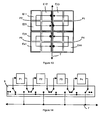
- each pixel (schematized by a circle) is, as before, connected to zero, while its output (shown schematically by a arrow) is connected to the bus 7.
- the detection circuit is provided with switches 8, controlled by the control circuit. control, not shown, allowing to connect at will the different pixels.
- the summation path within each pixel is preferably such that the input and the output of the pixel are both arranged on the same side, or access side, of the pixel, near the central bus. 7.
- the inputs and outputs of pixels P2 and P3 are all aligned in column 2, to the left of bus 7, while the inputs and outputs of pixels P1 and P4 are all aligned in column 3, to the right of the bus.
- switches selectively connect the input of each pixel to zero or the output of the previous pixel, and other switches selectively connect the output of each pixel to the bus 7 or the input of the next pixel.
- the pixel input P1, constituting the pixel cluster input is connected to zero
- the pixel output P4, constituting the pixel cluster output is connected to the bus 7.
- the pixel outputs, P1, P2 and P3 are respectively connected to the inputs of the following pixels P2, P3 and P4.
- the spatial resolution of the grouping is then equal to a quarter of the spatial resolution of the detection circuit according to the figure 13 , consisting of 4 independent pixels.
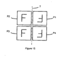
- FIG. figure 15 An appropriate arrangement of four pixels P1 to P4 for passing from a standard resolution, in which all the pixels are independent, to a group of pixels, having a reduced resolution, is represented in FIG. figure 15 .
- N being an even number
- the assembly thus forms a square of N 2 elementary circuits.
- the four pixels can be independent or grouped together, by switches 8, to form a grouping of pixels of reduced resolution.
- pixels may be distributed in the form of a matrix that is symmetrical with respect to the bus 7.
- the pixels P2 and P3 are respectively arranged at the top and at the bottom on the left of the bus 7, while the pixels P1 and P4 are respectively arranged at the top and at the bottom on the right of the bus 7.
- the serial link between the circuits of summation 6 of the elementary circuits E of a pixel P defines the summation path of the pixel.
- the summation path of the pixel P3 (represented diagrammatically by an F) is obtained by translation, parallel to the bus 7, of the summation path of the pixel P2 and vice versa.
- the summation paths of the pixels P1 and P4 are obtained by rotating 180 °, respectively from the pixels P2 and P3.
- the summation path of a pixel of the matrix can be obtained by translation, axial symmetry or rotation of 180 ° from the summation path of another pixel of the matrix. This symmetry makes it possible in particular to simplify the manufacture of a detection circuit comprising a large number of pixels and to modify, as required, the spatial resolution of the circuit.
Landscapes
- General Physics & Mathematics (AREA)
- Physics & Mathematics (AREA)
- Health & Medical Sciences (AREA)
- Life Sciences & Earth Sciences (AREA)
- High Energy & Nuclear Physics (AREA)
- Molecular Biology (AREA)
- Spectroscopy & Molecular Physics (AREA)
- Multimedia (AREA)
- Signal Processing (AREA)
- Engineering & Computer Science (AREA)
- Image Analysis (AREA)
- Transforming Light Signals Into Electric Signals (AREA)
- Measurement Of Radiation (AREA)
Claims (10)
- Schaltkreis zur Detektion von Teilchen mit einer Vielzahl von Einzelschaltkreisen (E), die jeweils ein Detektorelement (1) für Teilchen (p) aufweisen, das mit zugehörigen Zähleinrichtungen (4) verbunden ist, die Zählsignale liefern, welche repräsentativ sind für die Anzahl der von dem entsprechenden Detektorelement erfassten Teilchen, wobei der Schaltkreis dadurch gekennzeichnet ist, dass jeder Einzelschaltkreis (E) einen Summierschaltkreis (5) mit einem ersten und einem zweiten Eingang und einem Ausgang besitzt, wobei der erste Eingang des Summierschaltkreises (5) eines Einzelschaltkreises (E) mit dem Ausgang der zugehörigen Zähleinrichtungen (4) verbunden ist, wobei eine vorgegebene Anzahl von Einzelschaltkreisen (E) ein Pixel (P) darstellt, in dem die Summierschaltkreise (5) in Reihe geschaltet sind, zwischen einem Pixeleingang, der durch den zweiten Eingang des Summierschaltkreises eines ersten Einzelschaltkreises des Pixels gebildet ist, und einem Pixelausgang, der durch den Ausgang des Summierschaltkreises eines letzten Einzelschaltkreises des Pixels gebildet ist, und Zählsignale liefert, die repräsentativ sind für die Anzahl der von der Gesamtheit der Einzelschaltkreise des Pixels (P) erfassten Teilchen.
- Schaltkreis nach Anspruch 1, dadurch gekennzeichnet, dass jeder Einzelschaltkreis (E) Einrichtungen (6, R1) zum selektiven Zurücksetzen auf Null des ersten Eingangs des entsprechenden Summierschaltkreises (5) besitzt.
- Schaltkreis nach Anspruch 2, dadurch gekennzeichnet, dass die Einrichtungen zum Zurücksetzen auf Null einen Pufferspeicher (6) aufweisen, der zwischen dem Ausgang der Zähleinriclrtungen (4) und dem ersten Eingang des entsprechenden Summierschaltkreises (5) und einem Eingang (R1) für das Zurücksetzen auf Null des Pufferspeichers (6) angeschlossen ist.
- Schaltkreis nach einem der Ansprüche 1 bis 3, dadurch gekennzeichnet, dass er Schaltelemente (8) aufweist, die dazu dienen, den Eingang eines Pixels selektiv auf Null zu schalten oder an den Ausgang eines vorhergehenden Pixels abzuschließen.
- Schaltkreis nach Anspruch 4, dadurch gekennzeichnet, dass er Schaltelemente (8) aufweist, die dazu dienen, den Ausgang eines Pixels an einen Bus (7) oder an den Eingang des nachfolgenden Pixels anzuschließen.
- Schaltkreis nach einem der Ansprüche 1 bis 5, dadurch gekennzeichnet, dass der Eingang eines Pixels (P) auf Null geschaltet ist, während sein Ausgang an einen Bus (7) angeschlossen ist.
- Schaltkreis nach Anspruch 5, dadurch gekennzeichnet, dass mindestens zwei Pixel (P1, P2, P3, P4) zwischen Null und dem Bus (7) durch die Schaltelemente (8) in Reihe geschaltet sind.
- Schaltkreis nach einem der Ansprüche 1 bis 7, dadurch gekennzeichnet, dass, wenn die Einzelschaltkreise (Eij) eines Pixels in Form einer Matrix von Zeilen (i) und Spalten (j) angeordnet sind, der Eingang und der Ausgang eines Pixels auf derselben Zugangsseite des Pixels angeordnet sind.
- Schaltkreis nach einem der Ansprüche 1 bis 8, dadurch gekennzeichnet, dass, wenn N eine gerade Zahl ist, vier Pixel (P1 bis P), die jeweils N/2xN/2 Einzelschaltkreise aufweisen, zu beiden Seiten eines Bus (7) angeordnet sind.
- Schaltkreis nach einem der Ansprüche 1 bis 9, dadurch gekennzeichnet, dass er eine Vielzahl von Pixeln (P1 bis P4) aufweist, die in Form einer symmetrischen Matrix gegenüber dem Bus (7) verteilt sind, und dass man, da die serielle Verbindung zwischen den Summierschaltkreisen der Einzelschaltkreise eines Pixels einen Summierweg des Pixels bildet, den Summierweg eines Pixels durch Translation, axiale Symmetrie oder Drehung um ausgehend von dem Summierweg eines anderen Pixels erhält.
Applications Claiming Priority (2)
| Application Number | Priority Date | Filing Date | Title |
|---|---|---|---|
| FR0411794A FR2877733B1 (fr) | 2004-11-05 | 2004-11-05 | Circuit de detection de particules avec des circuits elementaires constituant des sous-pixels |
| PCT/FR2005/002694 WO2006051179A1 (fr) | 2004-11-05 | 2005-10-27 | Circuit de détection de particules avec des circuits élémentaires constituant des sous-pixels |
Publications (2)
| Publication Number | Publication Date |
|---|---|
| EP1869499A1 EP1869499A1 (de) | 2007-12-26 |
| EP1869499B1 true EP1869499B1 (de) | 2013-05-15 |
Family
ID=34950219
Family Applications (1)
| Application Number | Title | Priority Date | Filing Date |
|---|---|---|---|
| EP05815036.8A Ceased EP1869499B1 (de) | 2004-11-05 | 2005-10-27 | Schaltkreis zur detektion von teilchen mit einzel-schaltkreisen, die unter-pixel darstellen |
Country Status (5)
| Country | Link |
|---|---|
| US (1) | US7652260B2 (de) |
| EP (1) | EP1869499B1 (de) |
| JP (1) | JP4926974B2 (de) |
| FR (1) | FR2877733B1 (de) |
| WO (1) | WO2006051179A1 (de) |
Families Citing this family (7)
| Publication number | Priority date | Publication date | Assignee | Title |
|---|---|---|---|---|
| US8306786B1 (en) * | 2010-06-18 | 2012-11-06 | Hrl Laboratories, Llc | Detector array for compressive sensing |
| DE102011077859B4 (de) * | 2011-06-21 | 2014-01-23 | Siemens Aktiengesellschaft | Quantenzählender Strahlungsdetektor |
| AU2012292250A1 (en) * | 2011-07-20 | 2014-01-23 | Dectris Ltd. | Photon counting imaging method and device with instant retrigger capability |
| JP2013036867A (ja) * | 2011-08-09 | 2013-02-21 | Nippon Telegr & Teleph Corp <Ntt> | ミリ波パッシブイメージング装置 |
| EP2871496B1 (de) | 2013-11-12 | 2020-01-01 | Samsung Electronics Co., Ltd | Strahlungsdetektor und Computertomografievorrichtung damit |
| JP7179479B2 (ja) * | 2017-04-13 | 2022-11-29 | キヤノンメディカルシステムズ株式会社 | X線ct装置 |
| DE102018221701A1 (de) * | 2018-12-13 | 2020-06-18 | Robert Bosch Gmbh | Verfahren zur Verarbeitung des Signals eines Partikelsensors, der nach dem Prinzip der laserinduzierten Inkandeszenz arbeitet, Anordnung zur Verarbeitung eines solchen Signals, sowie Partikelsensor |
Family Cites Families (5)
| Publication number | Priority date | Publication date | Assignee | Title |
|---|---|---|---|---|
| US5970115A (en) * | 1996-11-29 | 1999-10-19 | Varian Medical Systems, Inc. | Multiple mode digital X-ray imaging system |
| US9029793B2 (en) * | 1998-11-05 | 2015-05-12 | Siemens Aktiengesellschaft | Imaging device |
| FI111759B (fi) * | 2000-03-14 | 2003-09-15 | Planmed Oy | Anturijärjestelmä ja menetelmä digitaalisessa röntgenkuvantamisessa |
| JP2002172113A (ja) * | 2000-12-07 | 2002-06-18 | Shimadzu Corp | 多チャンネル型検出器のデータ収集システム |
| FR2847677B1 (fr) * | 2002-11-26 | 2005-01-07 | Commissariat Energie Atomique | Detecteur de particules et dispositif de comptage comprenant une pluralite de detecteurs de particules |
-
2004
- 2004-11-05 FR FR0411794A patent/FR2877733B1/fr not_active Expired - Fee Related
-
2005
- 2005-10-27 JP JP2007539604A patent/JP4926974B2/ja not_active Expired - Fee Related
- 2005-10-27 US US11/665,545 patent/US7652260B2/en active Active
- 2005-10-27 EP EP05815036.8A patent/EP1869499B1/de not_active Ceased
- 2005-10-27 WO PCT/FR2005/002694 patent/WO2006051179A1/fr not_active Ceased
Also Published As
| Publication number | Publication date |
|---|---|
| JP2008519278A (ja) | 2008-06-05 |
| US7652260B2 (en) | 2010-01-26 |
| EP1869499A1 (de) | 2007-12-26 |
| FR2877733A1 (fr) | 2006-05-12 |
| FR2877733B1 (fr) | 2007-01-12 |
| WO2006051179A1 (fr) | 2006-05-18 |
| US20090121145A1 (en) | 2009-05-14 |
| JP4926974B2 (ja) | 2012-05-09 |
Similar Documents
| Publication | Publication Date | Title |
|---|---|---|
| EP2477393B1 (de) | Bildanzeigevorrichtung mit großem dynamischem Bereich | |
| EP1704422A1 (de) | Strahlungsdetektionssystem mit doppelrücksetz-impulszählung | |
| EP2766990B1 (de) | Vorrichtung zur umwandlung von stromimpulsen in spannungsimpulse | |
| EP3069506B1 (de) | Pooling von zwei pixelspalten eines bilddetektors | |
| EP2622845B1 (de) | Bildgebungsvorrichtung mit ohmschem spannungsabfall von null bei einem datenleiter | |
| EP2708023A1 (de) | Vorrichtung zur adressierung von leitungen eines steuerkreises für eine aktive detektionsmatrix | |
| FR2877733A1 (fr) | Circuit de detection de particules avec des circuits elementaires constituant des sous-pixels | |
| EP0331546B1 (de) | Photoempfindlicher Matrix mit zwei Dioden pro Punkt ohne spezifischen Rückstellungsleiter | |
| EP3386186A1 (de) | Bilderfassungssensor | |
| EP3900323B1 (de) | Pixelmatrix mit schneller pixel-binning | |
| EP2727334A1 (de) | Pixelmatrix mit programmierbaren clustern | |
| WO2014132003A1 (fr) | Dispositif de traitement d'un signal delivre par un detecteur de rayonnement | |
| EP0149948B1 (de) | Photoempfindliche Festkörperanordnungen | |
| EP1900194A1 (de) | Mikroelektronisches bildaufnahmegerät mit asynchronem analog-digital-wandler | |
| EP1424568A2 (de) | Teilchendetektor und Zählvorrichtung mit einer Mehrzahl von Teilchendetektoren | |
| WO2014096433A1 (fr) | Procede de lecture d'un dispositif d'imagerie | |
| EP3026890B1 (de) | Steuerung der integrationszeit in einem lichtempfindlichen apparat | |
| FR3059805A1 (fr) | Dispositif et procede de modulation, synapse artificielle comportant ledit dispositif de modulation, procede de plasticite a court terme dans un reseau de neurones artificiels comportant ladite synapse artificielle | |
| FR3119707A1 (fr) | Détecteur numérique à intégration numérique de charges | |
| EP2786487A1 (de) | Vorrichtung zur regelung einer zufälligen strömung von spannungspulsen am eingang eines analog-digital-wandlers | |
| EP0645775A1 (de) | Elektronische Speicherschaltung mit sequentiellem Zugriff | |
| WO2010015787A1 (fr) | Matrice de cellules electroniques | |
| FR3023413B1 (fr) | Amelioration de la vitesse de regroupement d'informations dans un equipement electronique matriciel | |
| WO2009043887A1 (fr) | Matrice de pixels avec pixel dote d'une source de courant integree actionnee par la selection du pixel | |
| FR2937159A1 (fr) | Circuit integre comprenant une matrice de cellules electroniques et detecteur a pixels comportant un tel circuit |
Legal Events
| Date | Code | Title | Description |
|---|---|---|---|
| PUAI | Public reference made under article 153(3) epc to a published international application that has entered the european phase |
Free format text: ORIGINAL CODE: 0009012 |
|
| 17P | Request for examination filed |
Effective date: 20070418 |
|
| AK | Designated contracting states |
Kind code of ref document: A1 Designated state(s): DE GB IT |
|
| DAX | Request for extension of the european patent (deleted) | ||
| RBV | Designated contracting states (corrected) |
Designated state(s): DE GB IT |
|
| RAP1 | Party data changed (applicant data changed or rights of an application transferred) |
Owner name: COMMISSARIAT A L'ENERGIE ATOMIQUE ET AUX ENERGIES |
|
| GRAJ | Information related to disapproval of communication of intention to grant by the applicant or resumption of examination proceedings by the epo deleted |
Free format text: ORIGINAL CODE: EPIDOSDIGR1 |
|
| GRAP | Despatch of communication of intention to grant a patent |
Free format text: ORIGINAL CODE: EPIDOSNIGR1 |
|
| RIN1 | Information on inventor provided before grant (corrected) |
Inventor name: GLASSER, FRANCIS Inventor name: ROSTAING, JEAN-PIERRE Inventor name: AUDEBERT, PATRICK Inventor name: BILLOINT, OLIVIER |
|
| GRAS | Grant fee paid |
Free format text: ORIGINAL CODE: EPIDOSNIGR3 |
|
| GRAA | (expected) grant |
Free format text: ORIGINAL CODE: 0009210 |
|
| AK | Designated contracting states |
Kind code of ref document: B1 Designated state(s): DE GB IT |
|
| REG | Reference to a national code |
Ref country code: GB Ref legal event code: FG4D Free format text: NOT ENGLISH |
|
| REG | Reference to a national code |
Ref country code: DE Ref legal event code: R096 Ref document number: 602005039622 Country of ref document: DE Effective date: 20130711 |
|
| PG25 | Lapsed in a contracting state [announced via postgrant information from national office to epo] |
Ref country code: IT Free format text: LAPSE BECAUSE OF FAILURE TO SUBMIT A TRANSLATION OF THE DESCRIPTION OR TO PAY THE FEE WITHIN THE PRESCRIBED TIME-LIMIT Effective date: 20130515 |
|
| PLBE | No opposition filed within time limit |
Free format text: ORIGINAL CODE: 0009261 |
|
| STAA | Information on the status of an ep patent application or granted ep patent |
Free format text: STATUS: NO OPPOSITION FILED WITHIN TIME LIMIT |
|
| 26N | No opposition filed |
Effective date: 20140218 |
|
| REG | Reference to a national code |
Ref country code: DE Ref legal event code: R097 Ref document number: 602005039622 Country of ref document: DE Effective date: 20140218 |
|
| PGFP | Annual fee paid to national office [announced via postgrant information from national office to epo] |
Ref country code: DE Payment date: 20211008 Year of fee payment: 17 Ref country code: GB Payment date: 20211020 Year of fee payment: 17 |
|
| REG | Reference to a national code |
Ref country code: DE Ref legal event code: R119 Ref document number: 602005039622 Country of ref document: DE |
|
| GBPC | Gb: european patent ceased through non-payment of renewal fee |
Effective date: 20221027 |
|
| PG25 | Lapsed in a contracting state [announced via postgrant information from national office to epo] |
Ref country code: DE Free format text: LAPSE BECAUSE OF NON-PAYMENT OF DUE FEES Effective date: 20230503 |
|
| PG25 | Lapsed in a contracting state [announced via postgrant information from national office to epo] |
Ref country code: GB Free format text: LAPSE BECAUSE OF NON-PAYMENT OF DUE FEES Effective date: 20221027 |