EP1865570A1 - Schaltnetzwerk - Google Patents
Schaltnetzwerk Download PDFInfo
- Publication number
- EP1865570A1 EP1865570A1 EP05727556A EP05727556A EP1865570A1 EP 1865570 A1 EP1865570 A1 EP 1865570A1 EP 05727556 A EP05727556 A EP 05727556A EP 05727556 A EP05727556 A EP 05727556A EP 1865570 A1 EP1865570 A1 EP 1865570A1
- Authority
- EP
- European Patent Office
- Prior art keywords
- mems
- terminal
- voltage
- mems switches
- antenna
- Prior art date
- Legal status (The legal status is an assumption and is not a legal conclusion. Google has not performed a legal analysis and makes no representation as to the accuracy of the status listed.)
- Withdrawn
Links
Images


Classifications
-
- H—ELECTRICITY
- H01—ELECTRIC ELEMENTS
- H01P—WAVEGUIDES; RESONATORS, LINES, OR OTHER DEVICES OF THE WAVEGUIDE TYPE
- H01P1/00—Auxiliary devices
- H01P1/10—Auxiliary devices for switching or interrupting
- H01P1/12—Auxiliary devices for switching or interrupting by mechanical chopper
- H01P1/127—Strip line switches
-
- H—ELECTRICITY
- H01—ELECTRIC ELEMENTS
- H01P—WAVEGUIDES; RESONATORS, LINES, OR OTHER DEVICES OF THE WAVEGUIDE TYPE
- H01P1/00—Auxiliary devices
- H01P1/18—Phase-shifters
- H01P1/184—Strip line phase-shifters
-
- H—ELECTRICITY
- H01—ELECTRIC ELEMENTS
- H01Q—ANTENNAS, i.e. RADIO AERIALS
- H01Q7/00—Loop antennas with a substantially uniform current distribution around the loop and having a directional radiation pattern in a plane perpendicular to the plane of the loop
-
- H—ELECTRICITY
- H01—ELECTRIC ELEMENTS
- H01Q—ANTENNAS, i.e. RADIO AERIALS
- H01Q9/00—Electrically-short antennas having dimensions not more than twice the operating wavelength and consisting of conductive active radiating elements
- H01Q9/04—Resonant antennas
- H01Q9/06—Details
- H01Q9/14—Length of element or elements adjustable
-
- H—ELECTRICITY
- H01—ELECTRIC ELEMENTS
- H01Q—ANTENNAS, i.e. RADIO AERIALS
- H01Q9/00—Electrically-short antennas having dimensions not more than twice the operating wavelength and consisting of conductive active radiating elements
- H01Q9/04—Resonant antennas
- H01Q9/16—Resonant antennas with feed intermediate between the extremities of the antenna, e.g. centre-fed dipole
Definitions
- the present invention relates to a switch circuit constituted by a plurality of microelectromechanical systems (MEMS) switches having different drive voltages, which is employed in a microwave circuit or an antenna circuit, and for varying configuration of the microwave circuit or the antenna circuit based upon drive voltages.
- MEMS microelectromechanical systems
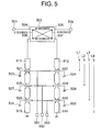
- FIG. 5 is a diagram for showing a configuration of the conventional microwave circuit (refer to, for instance, Non-patent Document 1).
- the conventional microwave circuit isprovided with Lange coupler 503 to which an input terminal 501 and an output terminal 502 are connected, and a signal circuit which is connected to coupling terminals 506 and 507 of the Lange coupler 503.
- an input terminal 504 connected to the input terminal 501 of the microwave circuit, an output terminal 505 connected to the output terminal 502 of the microwave circuit, the coupling terminal 506, and the coupling terminal 507 are connected.
- the signal circuit is provided with: a line 511, one end of which is connected to the coupling terminal 506, and another end of which is connected to a ground 513; a line 512, one end of which is connected to the coupling terminal 507, and another end of which is connected to a ground 514; MEMS switches 521, 525, and 529, which are connected to a midst of the line 511 in this order from a closer side with respect to the coupling terminal 506; MEMS switches 522, 526, and 530, which are connected to a midst of the line 512 in this order from closer with respect to the coupling terminal 507; a bias terminal 551, which is connected to the MEMS switch 521 and also to the MEMS switch 522; a bias terminal 552, which is connected to the MEMS switch 525 and also to the MEMS switch 526; and a bias terminal 553, which is connected to the MEMS switch 529 and also to the MEMS switch 530.
- Fig. 5 shows a circuit for a 2-bit phase shifter within a 4-bit phase shifter.
- the Lange coupler 503 outputs a half portion of a radio frequency signal entered from the input terminal 504 to the coupling terminal 506, and outputs the remaining half portion thereof to the coupling terminal 507.
- a phase of the signal outputted from the coupling terminal 507 is delayed by 90 degrees with respect to a phase of the signal outputted from the coupling terminal 506.
- the radio frequency signal outputted to the coupling terminal 506 is reflected by the MEMS switch 521, the MEMS switch 525, the MEMS switch 529, or the ground 513 being an end, passes again through the coupling terminal 506, and then a half signal portion thereof is outputted to the input terminal 504 and the remaining half portion thereof is outputted to the output terminal 505.
- a phase of the signal outputted from the output terminal 505 is delayed by 90 degrees with respect to a phase of the signal outputted from the input terminal 504.
- the radio frequency signal outputted to the coupling terminal 507 is reflected by the MEMS switch 522, the MEMS switch 526, the MEMS switch 530, or the ground 514 being an end, passes again through the coupling 507, and then a half portion thereof is outputted to the input terminal 504, and the remaining half portion thereof is outputted to the output terminal 505.
- a phase of the signal outputted from the input terminal 504 is delayed by 90 degrees with respect to a phase of the signal outputted from the output terminal 505.
- the MEMS switches 521 and 522 shortcircuit the lines 511 and 512 just at positions of the MEMS switches 521 and 522.
- the reflection waves reflected by the respective lines 511 and 512 are reflected based upon same reflection phases " ⁇ ".
- those signals are superimposed with each other.
- a phase of a signal which is propagated from the input terminal 501 through the input terminal 504, the coupling terminal 506, the MEMS switch 521, the coupling terminal 506, the input terminal 504, and the input terminal 501 in this order is opposite to a phase of another signal which is propagated from the input terminal 501 through the input terminal 504, the coupling terminal 507, the MEMS switch 522, the coupling terminal 507, the input terminal 504, and the input terminal 501 in this order.
- those signals are canceled with each other.
- phase delay amounts can be generated based on the selection of the below-mentioned four manners. That is, a voltage is applied to any one of the bias terminal 551, the bias terminal 552, and the bias terminal 553. Alternatively, the voltage is not applied to any of those bias terminals 551 to 553.
- a length of each of the lines 511 and 512 is equivalent to "L4", and a phase delay corresponds to a distance in which a radio signal is propagated, two times longer than the length "L4".
- a length of each of the lines 511 and 512 is equivalent to "L3", and a phase delay corresponds to a distance in which a radio signal is propagated two times longer than the length "L3".
- a length of each of the lines 511 and 512 is equivalent to "L2", and a phase delay corresponds to a distance in which a radio signal is propagated two times longer than the length "L2".
- a length of each of the lines 511 and 512 is equivalent to "L1"
- a phase delay corresponds to a distance in which a radio signal is propagated two times longer than the length "L1" .
- the above-mentioned circuit may be referred to as a phase shifter circuit for 2 bits, but requires at least three bias terminals 551 to 553.
- Non-patent Document 1 A. Malczewski, S. Eshelman, B. Pillans, J. Ehmke, and C. L. Goldsmith "X-Band RFMEMS Phase Shifters for Phased Array Applications", IEEE MICROWAVE AND GUIDED WAVE LETTERS, VOL. 9, NO. 12, DECEMBER 1999, pp. 517-519 .
- the present invention has been made to solve the above-mentioned problem, and it is an obj ect of the present invention to provide a switch circuit having bias terminals reduced in number, and being capable of readily changing a configuration of a circuit such as a microwave circuit or an antenna circuit.
- a switch circuit includes: a plurality of MEMS switches which are connected parallel to each other, and whose drive voltages are different from each other; and a single voltage source for driving the plurality of MEMS switches based upon a plurality of drive voltages.
- bias terminals can be reduced in number and the configuration of a circuit such as the microwave circuit or the antenna circuit can be readily changed, which are advantageous.
- Embodiment 1 describes such an example that a switch circuit is employed in a microwave circuit, while the switch circuit is configured by a plurality of MEMS switches having different drive voltages from each other.
- Embodiments 2 and 3 describe another example in which the above-mentioned switch circuit is employed in an antenna circuit. It shouldbe noted that a relationship between voltages (O ⁇ V1 ⁇ V2 ⁇ V3 ...) and lengths (0 ⁇ L1 ⁇ L2 ⁇ L3 ⁇ L4 ...) represents a relationship of relative magnitudes each of the embodiments. Accordingly, for example, the voltage "V1" of Embodiment 1 is not always equal to the voltage "V1" of Embodiment 2.
- FIG. 1 is a diagram for showing a configuration of the microwave circuit according to Embodiment 1 of the present invention.
- a 90-degree/3-dB coupler 3 and a signal circuit are provided in the microwave circuit according to Embodiment 1.
- An input terminal 1 and an output terminal 2 are connected to the 90-degrees/3-dB coupler 3.
- the signal circuit is connected to coupling terminals 6 and 7 of the 90-degrees/3-dB coupler 3.
- an input terminal 4 connected to the input terminal 1 of the microwave circuit, an output terminal 5 connected to the output terminal 2 of the microwave circuit, the coupling terminal 6, and the coupling terminal 7 are connected.
- the signal circuit is provided with: a line 11, one end of which is connected to the coupling terminal 6, and another end of which is connected to the ground 13; a line 12, one end of which is connected to the coupling terminal 7, and another end of which is connected to the ground 14; MEMS switches 21, 25, and 29, which are connected to a midst of the line 11 in this order from a closer side with respect to the coupling terminal 6; MEMS switches 22, 26, and 30, which are connected to a midst of the line 12 in this order from a closer side with respect to the coupling terminal 7; and a commonly-used voltage source 41, one end of which is connected via a bias terminal 43 to the MEMS switches 21, 22, 25, 26, 29, and 30, and another end of which is connected to the ground 42.
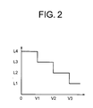
- Fig. 2 is a diagram for representing a relationship between voltages of bias terminals and lengths of lines up to the ground points of the microwave circuit according to Embodiment 1 of the present invention. It should be noted that, as to voltages, a relationship of 0 (volt) ⁇ V1 ⁇ V2 ⁇ V3 is established, and as to lengths, a relationship of 0 ⁇ L1 ⁇ L2 ⁇ L3 ⁇ L4 is established.
- the 90-degrees/3-dB coupler 3 outputs a half signal portion of a radio frequency signal entered from the input terminal 4 to the coupling terminal 6, and outputs the remaining half signal portion thereof to the coupling terminal 7.
- a phase of the signal outputted from the coupling terminal 7 is delayed by 90 degrees with respect to a phase of the signal outputted from the coupling terminal 6.
- the radio frequency signal outputted from the coupling terminal 6 is reflected by the MEMS switches 21, 25, and 29, or the ground 13 of a termination, and again passes through the coupling terminal 6, and then, a half signal portion thereof is outputted to the input terminal 4, and the remaining half signal portion thereof is outputted to the output terminal 5.
- a phase of the signal outputted from the output terminal 5 is delayed by 90 degrees with respect to a phase of the signal outputted from the input terminal 4.
- the radio frequency signal outputted from the coupling terminal 7 is reflected by the MEMS switches 22, 26, and 30, or the ground 14 of the termination, and again passes through the coupling terminal 7, and then, a half signal portion thereof is outputted to the input terminal 4, and the remaining half signal portion thereof is outputted to the output terminal 5.
- a phase of the signal outputted from the output terminal 5 is delayed by 90 degrees with respect to a phase of the signal outputted from the input terminal 4.
- a phase of a signal which is propagated from the input terminal 1 through the input terminal 4, the coupling terminal 6, the MEMS switch 21, the coupling terminal 6, the input terminal 4, and the input terminal 1 in this order is opposite to a phase of a signal which is propagated from the input terminal 1 through the input terminal 4, the coupling terminal 7, the MEMS switch 22, the coupling terminal 7, the input terminal 4, and the input terminal 1 in this order, so these signals are canceled with each other.
- phase delay amounts can be selected from the below-mentioned four manners. That is, the phase delay amounts can be selected from zero volt (0 V), V1, V2, and V3 of the voltages applied to the bias terminal 43.
- the line 12 When the voltage V3 is applied from the voltage source 41 to the bias terminal 43, the line 12 is connected to the ground 24 by the MEMS switch 22, and as represented in Figs. 1 and 2, an equivalent length of the line 12 becomes "L1". In this case, as described above, the voltage relationship is 0V ⁇ V1 ⁇ V2 ⁇ V3. As a result, only one bias terminal 43 is sufficient.
- theMEMS switches 29 and 30 which are located close to the terminations of the lines 11 and 12 are driven by the lower drive voltage, and the MEMS switches 21 and 22 which are located close to the input ends of the lines 11 and 12 are driven by the higher drive voltage.
- the MEMS switches 29 and 30 which are located close to the terminations of the lines 11 and 12 may be driven by the higher drive voltage, and the MEMS switches 21 and 22 which are located close to the input ends of the lines 11 and 12 may be driven by the lower drive voltage.
- Fig. 3 is a diagram for showing a configuration of the antenna circuit according to Embodiment 2 of the present invention.
- the antenna circuit according to Embodiment 2 is provided with: an antenna 101, which is constituted by one set of comb-shaped conductor; a capacitor 102, which is sandwiched between comb teeth being a tip portion of the antenna 101; an MEMS switch 103, which is sandwiched between second comb teeth from the tip portion of the antenna 101, and has a large capacitance when a voltage applied to both ends of the MEMS switch 103 is equal to or higher than V1; an MEMS switch 104, which is sandwiched between third comb teeth from the tip portion of the antenna 101, and has a large capacitance when a voltage applied to both ends of the MEMS switch 104 is equal to or higher than V2; an MEMS switch 105, which is loaded between fourth comb teeth from the tip portion of the antenna 101, and has a large capacitance when a voltage applied to both ends of the MEMS switch 105 is equal to or higher than V3; and a voltage source 109, which drives the MEMS switches 103 to 105 between
- the antenna 101 is entered from the feeding points 107 and 108 to a lower plane of the ground 106, and is connected via the capacitors 110 and 111 to a wave source 112.
- the ground 113 of this wave source 112 has the same potential as that of the ground 106.
- the antenna 101 is connected by the capacitor 102 at the tip portion thereof, and is operated at a frequency which is approximated to a 1/2 wavelength of the length L4.
- the MEMS switch 103 When the voltage of the voltage source 109 is equal to or higher than V1 and lower than V2, the MEMS switch 103 has a large capacitance, through which a radio frequency signal can pass. As a consequence, the antenna 101 is connected by the MEMS switch 103 and is operated at a frequency which is approximated to a 1/2 wavelength of the length L3.
- the MEMS switch 104 When the voltage of the voltage source 109 is equal to or higher than V2 and lower than V3, the MEMS switch 104 has a large capacitance, through which a radio frequency signal can pass. As a consequence, the antenna 101 is connected by the MEMS switch 104, and is operated at a frequency which is approximated to a 1/2 wavelength of the length L2.
- the MEMS switch 105 When the voltage of the voltage source 109 is more than V3, the MEMS switch 105 has a large capacitance, through which a radio frequency signal can pass. As a consequence, the antenna 101 is connected by the MEMS switch 105, and is operated at a frequency which is approximated to a 1/2 wavelength of the length L1.
- MEMS switches 103 to 105 have the capacitances
- those MEMS switches may also be referred to as MEMS capacitors 103 to 105.
- the operations of Embodiment 2 may be described as follows. That is, the drive voltage of the MEMS capacitor 103 having the small capacitance is made low, whereas the drive voltage of the MEMS capacitor 105 having the large capacitance is made high. Also, in an actual operation, the drive voltage of the MEMS capacitor 103 having the small capacitance may be made high, whereas the drive voltage of the MEMS capacitor 105 having the large capacitance may be made low.
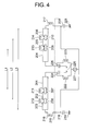
- Fig. 4 is a diagram for showing a configuration of the antenna circuit according to Embodiment 3 of the present invention.
- the antenna circuit according to Embodiment 3 is provided with: an antenna including antenna conductors 201, 202, 203, 204, 205, and 206; an MEMS switch 207 provided between the antenna conductors 201 and 202; an MEMS switch 208 provided between the antenna conductors 202 and 203; anMEMS switch 2 09 provided between the antenna conductors 204 and 205; anMEMS switch 210 provided between the antenna conductors 205 and 206; a coil 211 provided between the antenna conductors 201 and 202; a coil 212 provided between the antenna conductors 202 and 203; a coil 213 provided between the antenna conductors 204 and 205; a coil 214 provided between the antenna conductors 205 and 206; a coil 216 connected to the outermost side of the antenna conductor 203; and a coil 217 connected to the outermost side of the antenna conductor 206.
- the antenna conductors 201, 202, and 203 constitute one conductor of the antenna and are made of separate conductors. Also, the antenna conductors 204, 205, and 206 constitute the other conductor of the antenna and are made of separate conductors.
- a housing 215 contains: a capacitor 218, one end of which is connected to the coil 216 and another end of which is connected to a ground portion 219; a capacitor 220, one end of which is connected to the coil 217 and another end of which is connected to a ground portion 221; a coil 222, which is connected to the innermost side of the antenna conductor 201; a coil 223, which is connected to the innermost side of the antenna conductor 204; a voltage source 227, which applies a DC voltage between the coils 222 and 223, and between the coils 216 and 217; a capacitor 224, which is connected between the innermost side of the antenna conductor 201 and a radio frequency signal input/output terminal 226; and a capacitor 225, which is connected between the innermost side of the antenna conductor 204 and the radio frequency signal input/output terminal 226.
- Each of the MEMS switches 207 and 209 is designed in such a manner that when a voltage between both ends thereof is equal to or higher than V1, the MEMS switch is brought into a connection condition, whereas when a voltage between both ends thereof is lower than V1, the MEMS switch is brought into an open condition.
- each of the MEMS switches 208 and 210 is designed in such a manner that when a voltage between both ends thereof is equal to or higher than V2, the MEMS switch is brought into a connection condition, whereas when a voltage between both ends thereof is lower than V2, the MEMS switch is brought into an open condition.
- the antenna circuit is configured by two conductors, namely, one conductor to which the antenna conductors 201, 202, and 203 are connected, and another conductor to which the antenna conductors 204, 205, and 206 are connected.
- the antenna circuit is operated as a dipole antenna having a length of L3. Because all of those coils represent large resistances with respect to a radio frequency signal, the radio frequency signal cannot pass through all of those coils. Also, capacitance values of all of those capacitors are selected to be such values that a DC bias cannot pass through those capacitors.
- the antenna circuit is configured by two conductors, namely, one conductor to which the antenna conductors 201 and 202 are connected, and another conductor to which the antenna conductors 204 and 205 are connected.
- the antenna circuit is operated as a dipole antenna having a length of L2.
- the antenna circuit is configured by two conductors, namely, the antenna conductor 201 and the antenna conductor 204.
- the antenna circuit is operated as a dipole antenna having a length of L1.
Landscapes
- Variable-Direction Aerials And Aerial Arrays (AREA)
Applications Claiming Priority (1)
| Application Number | Priority Date | Filing Date | Title |
|---|---|---|---|
| PCT/JP2005/005900 WO2006106567A1 (ja) | 2005-03-29 | 2005-03-29 | スイッチ回路 |
Publications (2)
| Publication Number | Publication Date |
|---|---|
| EP1865570A1 true EP1865570A1 (de) | 2007-12-12 |
| EP1865570A4 EP1865570A4 (de) | 2008-07-16 |
Family
ID=37073136
Family Applications (1)
| Application Number | Title | Priority Date | Filing Date |
|---|---|---|---|
| EP05727556A Withdrawn EP1865570A4 (de) | 2005-03-29 | 2005-03-29 | Schaltnetzwerk |
Country Status (4)
| Country | Link |
|---|---|
| US (1) | US20090027138A1 (de) |
| EP (1) | EP1865570A4 (de) |
| JP (1) | JPWO2006106567A1 (de) |
| WO (1) | WO2006106567A1 (de) |
Families Citing this family (4)
| Publication number | Priority date | Publication date | Assignee | Title |
|---|---|---|---|---|
| WO2009081179A1 (en) * | 2007-12-21 | 2009-07-02 | Bae Systems Plc | Microwave coupler |
| JP6478397B2 (ja) * | 2015-03-13 | 2019-03-06 | 国立大学法人山形大学 | フェーズドアレイアンテナ |
| US12155128B2 (en) | 2022-01-04 | 2024-11-26 | Wisconsin Alumni Research Foundation | Electronically reconfigurable 1-bit phase quantization phased array element |
| US12183986B2 (en) | 2022-01-04 | 2024-12-31 | Wisconsin Alumni Research Foundation | Electronically reconfigurable 2-bit phase quantization phased array element |
Family Cites Families (13)
| Publication number | Priority date | Publication date | Assignee | Title |
|---|---|---|---|---|
| US4843358A (en) * | 1987-05-19 | 1989-06-27 | General Electric Company | Electrically positionable short-circuits |
| GB2239142A (en) * | 1989-12-15 | 1991-06-19 | Philips Electronic Associated | Variable bi-phase modulator circuits and variable resistors |
| US5349312A (en) * | 1993-05-28 | 1994-09-20 | Raytheon Company | Voltage variable attenuator |
| US5619061A (en) * | 1993-07-27 | 1997-04-08 | Texas Instruments Incorporated | Micromechanical microwave switching |
| US5526172A (en) * | 1993-07-27 | 1996-06-11 | Texas Instruments Incorporated | Microminiature, monolithic, variable electrical signal processor and apparatus including same |
| EP0661814B1 (de) * | 1993-12-28 | 1999-03-31 | STMicroelectronics S.r.l. | Zähl-Ende Detektionsvorrichtung, insbesondere für nicht flüchtige Speicher |
| US5428320A (en) * | 1994-08-29 | 1995-06-27 | Motorola, Inc. | Biphase modulator and method without matching elements |
| JP3333424B2 (ja) * | 1997-03-31 | 2002-10-15 | 三菱電機株式会社 | ダイバーシチ装置及びこの装置を使用した携帯無線機 |
| US6580337B1 (en) * | 1999-07-19 | 2003-06-17 | California Institute Of Technology | MEMS switch |
| US6639488B2 (en) * | 2001-09-07 | 2003-10-28 | Ibm Corporation | MEMS RF switch with low actuation voltage |
| US7151501B2 (en) * | 2003-02-21 | 2006-12-19 | Kyocera Wireless Corp. | Microelectromechanical switch (MEMS) antenna |
| JP2004282150A (ja) * | 2003-03-12 | 2004-10-07 | Sony Corp | 移相器及びフェーズドアレイアンテナ装置 |
| US7129805B2 (en) * | 2005-02-01 | 2006-10-31 | Continental Microwave & Tool Company, Inc. | Method of increasing the operating frequency in a series-shunt configured PIN diode switch |
-
2005
- 2005-03-29 US US11/886,589 patent/US20090027138A1/en not_active Abandoned
- 2005-03-29 JP JP2007512371A patent/JPWO2006106567A1/ja active Pending
- 2005-03-29 WO PCT/JP2005/005900 patent/WO2006106567A1/ja not_active Ceased
- 2005-03-29 EP EP05727556A patent/EP1865570A4/de not_active Withdrawn
Also Published As
| Publication number | Publication date |
|---|---|
| JPWO2006106567A1 (ja) | 2008-09-11 |
| EP1865570A4 (de) | 2008-07-16 |
| WO2006106567A1 (ja) | 2006-10-12 |
| US20090027138A1 (en) | 2009-01-29 |
Similar Documents
| Publication | Publication Date | Title |
|---|---|---|
| Malczewski et al. | X-band RF MEMS phase shifters for phased array applications | |
| US20250125790A1 (en) | Low loss reflective passive phase shifter using time delay element with double resolution | |
| US5121090A (en) | Balun providing dual balanced outputs | |
| US4205282A (en) | Phase shifting circuit element | |
| US5274343A (en) | Plural switch circuits having RF propagation networks and RF terminations | |
| US5208564A (en) | Electronic phase shifting circuit for use in a phased radar antenna array | |
| US20090278624A1 (en) | Reflection-type phase shifter having reflection loads implemented using transmission lines and phased-array receiver/transmitter utilizing the same | |
| US4751744A (en) | Monolithic distributed mixer | |
| US6335665B1 (en) | Adjustable phase and delay shift element | |
| US6320480B1 (en) | Wideband low-loss variable delay line and phase shifter | |
| JP2004527946A (ja) | 連続的に整調可能な位相器 | |
| KR20010031580A (ko) | 2주파 정합 회로 | |
| KR100526239B1 (ko) | 3 라인 발룬 트랜스포머 | |
| US5148128A (en) | RF digital phase shift modulators | |
| EP1865570A1 (de) | Schaltnetzwerk | |
| US5166648A (en) | Digital phase shifter apparatus | |
| US5416451A (en) | Circuit and method for balun compensation | |
| US6985049B2 (en) | Switched coupler type digital phase shifter using quadrature generator | |
| JP2962771B2 (ja) | 移相器 | |
| US4207547A (en) | Reflection mode notch filter | |
| US6556096B1 (en) | Artificial line | |
| JP2003264403A (ja) | マイクロ波移相器 | |
| US20040085112A1 (en) | Phase shift circuit and pahse shifter | |
| KR20070110393A (ko) | 스위치 회로 | |
| US7173503B1 (en) | Multibit phase shifter with active and passive phase bits, and active phase bit therefor |
Legal Events
| Date | Code | Title | Description |
|---|---|---|---|
| PUAI | Public reference made under article 153(3) epc to a published international application that has entered the european phase |
Free format text: ORIGINAL CODE: 0009012 |
|
| 17P | Request for examination filed |
Effective date: 20070914 |
|
| AK | Designated contracting states |
Kind code of ref document: A1 Designated state(s): DE FR GB |
|
| RIN1 | Information on inventor provided before grant (corrected) |
Inventor name: NISHINO, TAMOTSU, MITSUBISHI ELECTR.CORP. Inventor name: NISHIZAWA, KAZUSHI, MITSUBISHI ELECTR.CORP. Inventor name: TAKAHASHI, TOMOHIRO, MITSUBISHI ELECTR.CORP. Inventor name: MIYAZAKI, MORIYASU, MITSUBISHI ELECTRIC CORP. Inventor name: IZUO, SHINICHI, MITSUBISHI ELECTRIC CORP. Inventor name: KOGA, YOKO, MITSUBISHI ELECTRIC CORP. Inventor name: TAKETOMI, HIROKAZU, MITSUBISHI ELECTR.CORP. Inventor name: SODA, SHINNOSUKE, MITSUBISHI ELECTR.CORP. Inventor name: MIYAGUCHI, KENICHI, MITSUBISHI ELECTR.CORP. Inventor name: OHNO, ARAKI, MITSUBISHI ELECTRIC CORP. Inventor name: KODAMA, KENICHIRO, MITSUBISHI ELECTR.CORP. Inventor name: YOSHIDA, YUKIHISA, MITSUBISHI ELECTR.CORP. Inventor name: HANGAI, MASATAKE, MITSUBISHI ELECTR.CORP. |
|
| DAX | Request for extension of the european patent (deleted) | ||
| RBV | Designated contracting states (corrected) |
Designated state(s): DE FR GB |
|
| A4 | Supplementary search report drawn up and despatched |
Effective date: 20080613 |
|
| RIC1 | Information provided on ipc code assigned before grant |
Ipc: H01Q 9/16 20060101ALI20080609BHEP Ipc: H01Q 5/00 20060101ALI20080609BHEP Ipc: H01Q 5/02 20060101ALI20080609BHEP Ipc: H01P 1/12 20060101AFI20061019BHEP Ipc: H01Q 7/00 20060101ALI20080609BHEP |
|
| 17Q | First examination report despatched |
Effective date: 20080909 |
|
| STAA | Information on the status of an ep patent application or granted ep patent |
Free format text: STATUS: THE APPLICATION IS DEEMED TO BE WITHDRAWN |
|
| 18D | Application deemed to be withdrawn |
Effective date: 20090320 |