EP1863038A1 - Composite dielectric sheet, method for manufacturing same and multilayer electronic component - Google Patents
Composite dielectric sheet, method for manufacturing same and multilayer electronic component Download PDFInfo
- Publication number
- EP1863038A1 EP1863038A1 EP06712764A EP06712764A EP1863038A1 EP 1863038 A1 EP1863038 A1 EP 1863038A1 EP 06712764 A EP06712764 A EP 06712764A EP 06712764 A EP06712764 A EP 06712764A EP 1863038 A1 EP1863038 A1 EP 1863038A1
- Authority
- EP
- European Patent Office
- Prior art keywords
- composite dielectric
- sheet
- dielectric
- polyvinyl acetal
- dielectric constant
- Prior art date
- Legal status (The legal status is an assumption and is not a legal conclusion. Google has not performed a legal analysis and makes no representation as to the accuracy of the status listed.)
- Granted
Links
Images

Classifications
-
- H—ELECTRICITY
- H05—ELECTRIC TECHNIQUES NOT OTHERWISE PROVIDED FOR
- H05K—PRINTED CIRCUITS; CASINGS OR CONSTRUCTIONAL DETAILS OF ELECTRIC APPARATUS; MANUFACTURE OF ASSEMBLAGES OF ELECTRICAL COMPONENTS
- H05K1/00—Printed circuits
- H05K1/02—Details
- H05K1/03—Use of materials for the substrate
- H05K1/0313—Organic insulating material
- H05K1/0353—Organic insulating material consisting of two or more materials, e.g. two or more polymers, polymer + filler, + reinforcement
- H05K1/0373—Organic insulating material consisting of two or more materials, e.g. two or more polymers, polymer + filler, + reinforcement containing additives, e.g. fillers
-
- C—CHEMISTRY; METALLURGY
- C08—ORGANIC MACROMOLECULAR COMPOUNDS; THEIR PREPARATION OR CHEMICAL WORKING-UP; COMPOSITIONS BASED THEREON
- C08L—COMPOSITIONS OF MACROMOLECULAR COMPOUNDS
- C08L29/00—Compositions of homopolymers or copolymers of compounds having one or more unsaturated aliphatic radicals, each having only one carbon-to-carbon double bond, and at least one being terminated by an alcohol, ether, aldehydo, ketonic, acetal or ketal radical; Compositions of hydrolysed polymers of esters of unsaturated alcohols with saturated carboxylic acids; Compositions of derivatives of such polymers
- C08L29/14—Homopolymers or copolymers of acetals or ketals obtained by polymerisation of unsaturated acetals or ketals or by after-treatment of polymers of unsaturated alcohols
-
- H—ELECTRICITY
- H01—ELECTRIC ELEMENTS
- H01B—CABLES; CONDUCTORS; INSULATORS; SELECTION OF MATERIALS FOR THEIR CONDUCTIVE, INSULATING OR DIELECTRIC PROPERTIES
- H01B3/00—Insulators or insulating bodies characterised by the insulating materials; Selection of materials for their insulating or dielectric properties
- H01B3/18—Insulators or insulating bodies characterised by the insulating materials; Selection of materials for their insulating or dielectric properties mainly consisting of organic substances
- H01B3/30—Insulators or insulating bodies characterised by the insulating materials; Selection of materials for their insulating or dielectric properties mainly consisting of organic substances plastics; resins; waxes
- H01B3/44—Insulators or insulating bodies characterised by the insulating materials; Selection of materials for their insulating or dielectric properties mainly consisting of organic substances plastics; resins; waxes vinyl resins; acrylic resins
- H01B3/446—Insulators or insulating bodies characterised by the insulating materials; Selection of materials for their insulating or dielectric properties mainly consisting of organic substances plastics; resins; waxes vinyl resins; acrylic resins from vinylacetals
-
- H—ELECTRICITY
- H01—ELECTRIC ELEMENTS
- H01G—CAPACITORS; CAPACITORS, RECTIFIERS, DETECTORS, SWITCHING DEVICES, LIGHT-SENSITIVE OR TEMPERATURE-SENSITIVE DEVICES OF THE ELECTROLYTIC TYPE
- H01G4/00—Fixed capacitors; Processes of their manufacture
- H01G4/002—Details
- H01G4/018—Dielectrics
- H01G4/20—Dielectrics using combinations of dielectrics from more than one of groups H01G4/02 - H01G4/06
- H01G4/206—Dielectrics using combinations of dielectrics from more than one of groups H01G4/02 - H01G4/06 inorganic and synthetic material
-
- H—ELECTRICITY
- H01—ELECTRIC ELEMENTS
- H01G—CAPACITORS; CAPACITORS, RECTIFIERS, DETECTORS, SWITCHING DEVICES, LIGHT-SENSITIVE OR TEMPERATURE-SENSITIVE DEVICES OF THE ELECTROLYTIC TYPE
- H01G4/00—Fixed capacitors; Processes of their manufacture
- H01G4/30—Stacked capacitors
-
- C—CHEMISTRY; METALLURGY
- C08—ORGANIC MACROMOLECULAR COMPOUNDS; THEIR PREPARATION OR CHEMICAL WORKING-UP; COMPOSITIONS BASED THEREON
- C08L—COMPOSITIONS OF MACROMOLECULAR COMPOUNDS
- C08L63/00—Compositions of epoxy resins; Compositions of derivatives of epoxy resins
-
- H—ELECTRICITY
- H05—ELECTRIC TECHNIQUES NOT OTHERWISE PROVIDED FOR
- H05K—PRINTED CIRCUITS; CASINGS OR CONSTRUCTIONAL DETAILS OF ELECTRIC APPARATUS; MANUFACTURE OF ASSEMBLAGES OF ELECTRICAL COMPONENTS
- H05K1/00—Printed circuits
- H05K1/16—Printed circuits incorporating printed electric components, e.g. printed resistors, capacitors or inductors
- H05K1/162—Printed circuits incorporating printed electric components, e.g. printed resistors, capacitors or inductors incorporating printed capacitors
-
- H—ELECTRICITY
- H05—ELECTRIC TECHNIQUES NOT OTHERWISE PROVIDED FOR
- H05K—PRINTED CIRCUITS; CASINGS OR CONSTRUCTIONAL DETAILS OF ELECTRIC APPARATUS; MANUFACTURE OF ASSEMBLAGES OF ELECTRICAL COMPONENTS
- H05K2201/00—Indexing scheme relating to printed circuits covered by H05K1/00
- H05K2201/02—Fillers; Particles; Fibers; Reinforcement materials
- H05K2201/0203—Fillers and particles
- H05K2201/0206—Materials
- H05K2201/0209—Inorganic, non-metallic particles
-
- H—ELECTRICITY
- H05—ELECTRIC TECHNIQUES NOT OTHERWISE PROVIDED FOR
- H05K—PRINTED CIRCUITS; CASINGS OR CONSTRUCTIONAL DETAILS OF ELECTRIC APPARATUS; MANUFACTURE OF ASSEMBLAGES OF ELECTRICAL COMPONENTS
- H05K2201/00—Indexing scheme relating to printed circuits covered by H05K1/00
- H05K2201/02—Fillers; Particles; Fibers; Reinforcement materials
- H05K2201/0203—Fillers and particles
- H05K2201/0206—Materials
- H05K2201/0239—Coupling agent for particles
-
- Y—GENERAL TAGGING OF NEW TECHNOLOGICAL DEVELOPMENTS; GENERAL TAGGING OF CROSS-SECTIONAL TECHNOLOGIES SPANNING OVER SEVERAL SECTIONS OF THE IPC; TECHNICAL SUBJECTS COVERED BY FORMER USPC CROSS-REFERENCE ART COLLECTIONS [XRACs] AND DIGESTS
- Y10—TECHNICAL SUBJECTS COVERED BY FORMER USPC
- Y10T—TECHNICAL SUBJECTS COVERED BY FORMER US CLASSIFICATION
- Y10T428/00—Stock material or miscellaneous articles
- Y10T428/249921—Web or sheet containing structurally defined element or component
- Y10T428/249953—Composite having voids in a component [e.g., porous, cellular, etc.]
-
- Y—GENERAL TAGGING OF NEW TECHNOLOGICAL DEVELOPMENTS; GENERAL TAGGING OF CROSS-SECTIONAL TECHNOLOGIES SPANNING OVER SEVERAL SECTIONS OF THE IPC; TECHNICAL SUBJECTS COVERED BY FORMER USPC CROSS-REFERENCE ART COLLECTIONS [XRACs] AND DIGESTS
- Y10—TECHNICAL SUBJECTS COVERED BY FORMER USPC
- Y10T—TECHNICAL SUBJECTS COVERED BY FORMER US CLASSIFICATION
- Y10T428/00—Stock material or miscellaneous articles
- Y10T428/25—Web or sheet containing structurally defined element or component and including a second component containing structurally defined particles
-
- Y—GENERAL TAGGING OF NEW TECHNOLOGICAL DEVELOPMENTS; GENERAL TAGGING OF CROSS-SECTIONAL TECHNOLOGIES SPANNING OVER SEVERAL SECTIONS OF THE IPC; TECHNICAL SUBJECTS COVERED BY FORMER USPC CROSS-REFERENCE ART COLLECTIONS [XRACs] AND DIGESTS
- Y10—TECHNICAL SUBJECTS COVERED BY FORMER USPC
- Y10T—TECHNICAL SUBJECTS COVERED BY FORMER US CLASSIFICATION
- Y10T428/00—Stock material or miscellaneous articles
- Y10T428/29—Coated or structually defined flake, particle, cell, strand, strand portion, rod, filament, macroscopic fiber or mass thereof
- Y10T428/2982—Particulate matter [e.g., sphere, flake, etc.]
- Y10T428/2984—Microcapsule with fluid core [includes liposome]
-
- Y—GENERAL TAGGING OF NEW TECHNOLOGICAL DEVELOPMENTS; GENERAL TAGGING OF CROSS-SECTIONAL TECHNOLOGIES SPANNING OVER SEVERAL SECTIONS OF THE IPC; TECHNICAL SUBJECTS COVERED BY FORMER USPC CROSS-REFERENCE ART COLLECTIONS [XRACs] AND DIGESTS
- Y10—TECHNICAL SUBJECTS COVERED BY FORMER USPC
- Y10T—TECHNICAL SUBJECTS COVERED BY FORMER US CLASSIFICATION
- Y10T428/00—Stock material or miscellaneous articles
- Y10T428/31504—Composite [nonstructural laminate]
-
- Y—GENERAL TAGGING OF NEW TECHNOLOGICAL DEVELOPMENTS; GENERAL TAGGING OF CROSS-SECTIONAL TECHNOLOGIES SPANNING OVER SEVERAL SECTIONS OF THE IPC; TECHNICAL SUBJECTS COVERED BY FORMER USPC CROSS-REFERENCE ART COLLECTIONS [XRACs] AND DIGESTS
- Y10—TECHNICAL SUBJECTS COVERED BY FORMER USPC
- Y10T—TECHNICAL SUBJECTS COVERED BY FORMER US CLASSIFICATION
- Y10T428/00—Stock material or miscellaneous articles
- Y10T428/31504—Composite [nonstructural laminate]
- Y10T428/31511—Of epoxy ether
-
- Y—GENERAL TAGGING OF NEW TECHNOLOGICAL DEVELOPMENTS; GENERAL TAGGING OF CROSS-SECTIONAL TECHNOLOGIES SPANNING OVER SEVERAL SECTIONS OF THE IPC; TECHNICAL SUBJECTS COVERED BY FORMER USPC CROSS-REFERENCE ART COLLECTIONS [XRACs] AND DIGESTS
- Y10—TECHNICAL SUBJECTS COVERED BY FORMER USPC
- Y10T—TECHNICAL SUBJECTS COVERED BY FORMER US CLASSIFICATION
- Y10T428/00—Stock material or miscellaneous articles
- Y10T428/31504—Composite [nonstructural laminate]
- Y10T428/31511—Of epoxy ether
- Y10T428/31515—As intermediate layer
- Y10T428/31522—Next to metal
Definitions
- crosslinking agent which has two or more functional groups, is a polyisocyanate.
- the crosslinking agent is usually added to a mixture of the high-dielectric constant filler and the organic solvent solution of the polyvinyl acetal resin.
- the following process can be used to form the slurry into a sheet-shaped piece: for example, a doctor blade process, a gravure printing process, or a die coating process.
- the amount of the polyisocyanate is preferably five weight parts or more and more preferably ten weight parts or more. If the amount of the polyisocyanate is less than five weight parts, the polyvinyl acetal resin and the epoxy resin cannot be sufficiently crosslinked to each other. This causes a reduction in dielectric strength and/or a reduction in heat resistance.
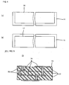
- the conductive layer 16 extends on the composite dielectric sheet 14 to form such a pattern as shown in Fig. 4(a) and the conductive layer 17 extends on the composite dielectric sheet 15 to form such a pattern as shown in Fig. 4(b). Therefore, although the composite dielectric sheets 14 and 15 are rolled together such that the laminate 12 is prepared, the conductive layers 16 and 17 are not in electrical contact with each other.
- Sample 12 was prepared in substantially the same manner as that for preparing Sample 7 except that the crosslinking agent used to prepare Sample 12 was a mixture of the epoxy resin and the phenol resin, which were curable resins, and the weight ratio of the epoxy resin to the phenol resin was 141 : 84.
- the crosslinking agent used to prepare Sample 12 was a mixture of the epoxy resin and the phenol resin, which were curable resins, and the weight ratio of the epoxy resin to the phenol resin was 141 : 84.
- the strontium titanate powder was surface-treated with the epoxy group-containing silane and was dispersed in the liquid mixture in such a manner that 100 weight parts of the strontium titanate powder, one weight part of the epoxy group-containing silane, and 80 weight parts of the liquid mixture were mixed in a ball mill for eight hours.
Landscapes
- Engineering & Computer Science (AREA)
- Power Engineering (AREA)
- Microelectronics & Electronic Packaging (AREA)
- Chemical & Material Sciences (AREA)
- Manufacturing & Machinery (AREA)
- Chemical Kinetics & Catalysis (AREA)
- Polymers & Plastics (AREA)
- Organic Chemistry (AREA)
- Medicinal Chemistry (AREA)
- Physics & Mathematics (AREA)
- Health & Medical Sciences (AREA)
- Spectroscopy & Molecular Physics (AREA)
- Inorganic Chemistry (AREA)
- Fixed Capacitors And Capacitor Manufacturing Machines (AREA)
- Compositions Of Macromolecular Compounds (AREA)
- Laminated Bodies (AREA)
- Inorganic Insulating Materials (AREA)
- Organic Insulating Materials (AREA)
Abstract
Description
- The present invention relates to a composite dielectric sheet, a method for producing the composite dielectric sheet, and a multilayer electronic component including the composite dielectric sheet. The present invention particularly relates to the improvement of dielectric properties of the composite dielectric sheet.
- Dielectric sheets are used to manufacture multilayer electronic components such as monolithic capacitors, rolled capacitors (film capacitors), and multilayer wiring boards. The dielectric sheets need to meet requirements below.
- For the size reduction of the multilayer electronic components, the dielectric sheets need to have large dielectric constants. Furthermore, the dielectric sheets need to have high dielectric strength if the dielectric sheets are used for electronic components, such as capacitors, for use in power supply circuits for power electronics such as fuel cells, wind power generators, and hybrid cars. The market of the power electronics is expanding because environmental issues are attracting much attention.
- Alternatively, the dielectric sheets need to be flexible if the dielectric sheets are used for rolled capacitors or flexible multilayer wiring boards that can follow the shape of surrounding members. Therefore, flexible films made of resin have been used for the above applications instead of the dielectric sheets.
- The resin usually has a dielectric constant of about two to five; hence, it is difficult to prepare flexible films having large dielectric constants using the resin. The following sheets have been proposed (for example,
Patent Documents 1 to 3): flexible composite dielectric sheets which have a large dielectric constant which contain resins and high-dielectric constant fillers, dispersed in the resins, containing high-dielectric constant components such as dielectric ceramic components. Since the composite dielectric sheets are flexible and have large dielectric constants, the composite dielectric sheets can meet requirements for size reduction. - In the composite dielectric sheets, the interfaces between the resins and the fillers are discontinuous and therefore may cause dielectric breakdown. Hence, there is a problem in that the composite dielectric sheets have low dielectric strength. If the fillers are not uniformly dispersed in the resins, the composite dielectric sheets have pores. This causes a problem that the composite dielectric sheets have low dielectric strength.
-
Patent Document 1 discloses a method for producing a composite dielectric sheet. In the method, a mixture of a molten resin and a filler is formed into a sheet-shaped piece by a dry process.Patent Documents - In order to solve the problems regarding low dielectric strength, the sheet formed by the dry process is hot-pressed such that the pores in the sheet are reduced as disclosed in
Patent Document 1. It is difficult to uniformly disperse the filler, of which the volume content is 20% or more, in the resin as long as the dry process is used; hence, it is substantially impossible for the composite dielectric sheet to have a dielectric constant of six or more. - The composite dielectric sheet disclosed in
Patent Document 2 has a large dielectric constant. AlthoughPatent Document 2 does not describe the dielectric strength of the composite dielectric sheet, the dielectric strength thereof is supposed to be low because no measure is taken to eliminate the discontinuity of the resin-filler interfaces. - The composite dielectric sheet disclosed in
Patent Document 3 has a large dielectric constant and is prepared in such a manner that the filler is surface-treated with a silane-coupling agent and the slurry is prepared by dispersing the resulting filler in a solution prepared by mixing polyphenylene oxide (PPO), a crosslinking resin, and a reaction initiator and is then formed into such a sheet-shaped piece. PPO has no reactive functional group and therefore has low adhesion with the crosslinking resin. Furthermore, the reaction initiator serves as an impurity. Hence, the dielectric strength of this composite dielectric sheet is supposed to be low. - Patent Document 1:
Japanese Unexamined Patent Application Publication No. 2000-294447 - Patent Document 2:
Japanese Unexamined Patent Application Publication No. 3-208324 - Patent Document 3:
Japanese Unexamined Patent Application Publication No. 6-52716 - It is an object of the present invention to provide a composite dielectric sheet capable of solving the above problems. In particular, the composite dielectric sheet is flexible and has a large dielectric constant and high dielectric strength. It is another object of the present invention to provide a method for producing the composite dielectric sheet.
- It is another object of the present invention to provide a multilayer electronic component including the composite dielectric sheet.
- In order to solve the above technical problems, a composite dielectric sheet according to the present invention contains a polyvinyl acetal resin; a high-dielectric constant filler, surface-treated with a coupling agent, dispersed in the polyvinyl acetal resin; and a crosslinking agent having two or more functional groups reactable with the polyvinyl acetal resin and the surface-treated high-dielectric constant filler.
- The coupling agent is preferably a silane coupling agent having an amino group or an epoxy group.
- The high-dielectric constant filler preferably has a dielectric constant of 10 or more.
- The crosslinking agent is preferably a polyisocyanate.
- The composite dielectric sheet may further contain an epoxy resin. In this case, the crosslinking agent preferably has functional groups reactable with the polyvinyl acetal resin, the surface-treated high-dielectric constant filler, and the epoxy resin.
- The present invention provides a method for producing the composite dielectric sheet. The method includes a step of preparing a slurry by mixing a solvent, a polyvinyl acetal resin, a high-dielectric constant filler surface-treated with a coupling agent, and a crosslinking agent having two or more functional groups reactable with the polyvinyl acetal resin and the surface-treated high-dielectric constant filler; a step of preparing an uncured sheet in such a manner that the slurry is formed into a sheet-shaped piece and the solvent is then vaporized; and a step of heating the uncured sheet such that a crosslinking reaction occurs therein.
- Furthermore, the present invention provides a multilayer electronic component including the composite dielectric sheet.
- The composite dielectric sheet contains the polyvinyl acetal resin and the high-dielectric constant filler, which is surface-treated with the coupling agent. Therefore, functional groups formed on the surface of the high-dielectric constant filler by the coupling agent are linked to functional groups of the polyvinyl acetal resin with the crosslinking agent having such two or more functional groups. This eliminates the discontinuity of the interface between the filler and the resin, the discontinuity causing dielectric breakdown.
- As is clear from experiments described below, the composite dielectric sheet has high dielectric strength at room temperature because the composite dielectric sheet contains the polyvinyl acetal resin.
- Therefore, the composite dielectric sheet has high dielectric strength. Furthermore, the composite dielectric sheet is flexible and has a large dielectric constant because the composite dielectric sheet contains the high-dielectric constant filler.
- Therefore, if the composite dielectric sheet is used to manufacture a multilayer electronic component, the multilayer electronic component has high dielectric strength. The composite dielectric sheet is effective in the size reduction of multilayer electronic components.
- The polyvinyl acetal resin is thermoplastic and can be formed into a film by the vaporization of a solvent. An uncured sheet prepared therefrom has sufficient strength and can be readily handled. The polyvinyl acetal resin is useful in preparing sheets at high speed. Therefore, the composite dielectric sheet can be produced at a high production rate.
- When the composite dielectric sheet further contains the epoxy resin, the composite dielectric sheet has high dielectric strength at high temperature.
- When the composite dielectric sheet contains the epoxy resin as described above, the crosslinking agent preferably has functional groups reactable with the polyvinyl acetal resin, the surface-treated high-dielectric constant filler, and the epoxy resin. The crosslinking agent is preferably a polyisocyanate regardless of whether the composite dielectric sheet contains the epoxy resin or not.
- A method for producing the composite dielectric sheet according to the present invention is as follows: a slurry is prepared by mixing a solvent, the polyvinyl acetal resin, the high-dielectric constant filler, and the crosslinking agent and is then formed into a sheet-shaped piece, the solvent is vaporized; and the sheet-shaped piece is heat-treated such that the composite dielectric sheet is obtained. Hence, the dispersion of the high-dielectric constant filler is fine and the sheet has substantially no pores.
- Thus, the method according to the present invention is effective in imparting high dielectric strength to the composite dielectric sheet.
- The polyvinyl acetal resin is thermoplastic and can be formed into a film by the vaporization of the solvent. An uncured sheet prepared therefrom has sufficient strength and can be readily handled. The polyvinyl acetal resin is useful in preparing sheets at high speed. Therefore, the composite dielectric sheet can be produced at a high production rate.
-
- [Fig. 1] Fig. 1 is a sectional view of a
monolithic capacitor 1 that is a first example of a multilayer electronic component including composite dielectric sheets according to the present invention. - [Fig. 2] Fig. 2 is a perspective view of one of the composite dielectric sheets having conductive layers 4 used to manufacturing the
monolithic capacitor 1 shown in Fig. 1. - [Fig. 3] Fig. 3 is a perspective view of a rolled
capacitor 11 that is a second example of the multilayer electronic component, which includes the composite dielectric sheets according to the present invention. - [Fig. 4] Fig. 4 includes plan views of the
composite dielectric sheets conductive layers capacitor 11 shown in Fig. 3. - [Fig. 5] Fig. 5 is a sectional view of a
multilayer wiring board 21 that is a third example of the multilayer electronic component, which includes the composite dielectric sheets according to the present invention. Reference Numerals- 1 monolithic capacitor
- 2, 12, and 23 laminates
- 3, 14, 15, and 22 composite dielectric sheets
- A composite dielectric sheet according to the present invention is preferably prepared in such a manner that a high-dielectric constant filler is surface-treated with a coupling agent so as to have reactive functional groups, the resulting high-dielectric constant filler and a crosslinking agent are added to an organic solvent solution of a polyvinyl acetal resin and are then sufficiently dispersed therein, and the dispersion is formed into a sheet-shaped piece, which is then heat-treated. The crosslinking agent has two or more functional groups for bonding the polyvinyl acetal resin and the high-dielectric constant filler together.
- The polyvinyl acetal resin has a hydroxyl group that is a reactive functional group. Examples of the polyvinyl acetal resin include polyvinyl butyral, polyvinyl formal, and a mixture thereof.
- The polyvinyl acetal resin has an acetal moiety with an alkyl group represented by the formula CnH2n+1, wherein n is preferably zero to four and more preferably zero or one. When n is greater than four, the polyvinyl acetal resin may have a low glass transition point and low heat resistance.
- Preferable examples of a material for forming the high-dielectric constant filler include dielectric ceramics such as barium titanate, calcium titanate, strontium titanate, calcium zirconate, and lead zirconate titanate.
- The high-dielectric constant filler preferably has an average particle size of 2 µm or less and more preferably 1 µm or less. The content of the high-dielectric constant filler in the composite dielectric sheet is preferably five to 50 volume percent. When the content thereof is less than five volume percent, the composite dielectric sheet has an insufficient dielectric constant. When the content thereof is greater than 50 volume percent, the composite dielectric sheet may have pores, which cause a reduction in dielectric strength.
- A preferable example of the coupling agent, which is used to surface-treat the high-dielectric constant filler, is a silane coupling agent having an amino group or an epoxy group. Another example of the coupling agent is a titanate having a hydroxy group. Before the high-dielectric constant filler is added to the organic solvent solution of the polyvinyl acetal resin, the high-dielectric constant filler is surface-treated with the coupling agent. Alternatively, the following process may be used to surface-treat the high-dielectric constant filler: an integral blending process in which the coupling agent is added to the slurry prepared by adding the untreated high-dielectric constant filler to the organic solvent solution of the polyvinyl acetal resin.
- An example of the crosslinking agent, which has two or more functional groups, is a polyisocyanate. The crosslinking agent is usually added to a mixture of the high-dielectric constant filler and the organic solvent solution of the polyvinyl acetal resin.
- In order to prepare the slurry by adding the high-dielectric constant filler and the crosslinking agent to the organic solvent solution of the polyvinyl acetal resin, these components are subjected to dispersion treatment. The following apparatus may be use to subject these components to dispersion treatment: a high pressure homogenizer or a medium-stirring mill, such as a ball mill or a sand mill, containing a mixing medium.
- The following process can be used to form the slurry into a sheet-shaped piece: for example, a doctor blade process, a gravure printing process, or a die coating process.
- The composite dielectric sheet according to the present invention may further contain an epoxy resin. In this case, if the crosslinking agent is a polyisocyanate having a functional group reactable with both of the polyvinyl acetal resin, which is thermoplastic, and the epoxy resin, which is heat-curable, the composite dielectric sheet exhibits high dielectric strength at an elevated temperature, for example, 150°C. This is probably because the crosslinking agent reacts with both of the thermoplastic resin and the heat-curable resin and therefore the resin has high heat resistance.
- The epoxy resin preferably has an epoxy equivalent of 150 to 300. When the epoxy equivalent thereof is less than 150, the crosslink density is low and therefore the heat resistance is insufficient. When the epoxy equivalent thereof is greater than 300, the number of hydroxy groups generated by reaction is large. This causes an increase in dielectric loss tangent and a reduction in heat resistance.
- When the sum of the amount of the polyvinyl acetal resin, the amount of the epoxy resin, and the amount of the polyisocyanate is 100 weight parts, the amount of the polyvinyl acetal resin is preferably 20 to 80 weight parts and more preferably 30 to 70 weight parts. If the amount of the polyvinyl acetal resin is less than 20 weight parts, there is a problem in that the slurry is difficult to dry and therefore the rate of forming a sheet is low. If the amount of the polyvinyl acetal resin is greater than 80 weight parts, the sum of the amount of the epoxy resin and the amount of the polyisocyanate is excessively small and therefore the heat resistance is insufficient.
- When the sum of the amount of the polyvinyl acetal resin, the amount of the epoxy resin, and the amount of the polyisocyanate is 100 weight parts, the amount of the epoxy resin is preferably five weight parts or more and more preferably ten weight parts or more. If the amount of the epoxy resin is less than five weight parts, the heat resistance is insufficient.
- When the sum of the amount of the polyvinyl acetal resin, the amount of the epoxy resin, and the amount of the polyisocyanate is 100 weight parts, the amount of the polyisocyanate is preferably five weight parts or more and more preferably ten weight parts or more. If the amount of the polyisocyanate is less than five weight parts, the polyvinyl acetal resin and the epoxy resin cannot be sufficiently crosslinked to each other. This causes a reduction in dielectric strength and/or a reduction in heat resistance.
- A multilayer electronic component including composite dielectric sheets according to the present invention will now be described.
- Fig. 1 is a sectional view of a
monolithic capacitor 1 that is a first example of the multilayer electronic component. - The
monolithic capacitor 1 includes alaminate 2 with a rectangular parallelepiped shape. Thelaminate 2 includes a plurality ofcomposite dielectric sheets 3 according to the present invention and conductive layers 4 each disposed between thecomposite dielectric sheets 3 next to each other. -
Terminal electrodes 5 are disposed on both end portions of thelaminate 2. Some of the conductive layers 4 extend to one of the end portions thereof and are electrically connected to one of theterminal electrodes 5. The other conductive layers 4 extend to the other one of the end portions thereof and are electrically connected to the other one of theterminal electrodes 5. The conductive layers 4 electrically connected to one of theterminal electrodes 5 and the conductive layers 4 connected to the other one are alternately arranged. A sub-capacitor formed between each pair of the conductive layers 4 that are opposed to each other with eachcomposite dielectric sheet 3 disposed therebetween is discharged through theterminal electrodes 5. - In order to manufacture the
monolithic capacitor 1, thecomposite dielectric sheets 3 having the conductive layers 4 thereon are prepared as shown in Fig. 2. The conductive layers 4 principally contain, for example, aluminum or zinc and can be formed by a vacuum vapor deposition process. The conductive layers 4 may each include a plurality of aluminum sublayers and zinc sublayers. With reference to Fig. 2, each conductive layer 4 does not reach one end of eachcomposite dielectric sheet 3. - The
composite dielectric sheets 3 shown in Fig. 2 are stacked, whereby thelaminate 2 is prepared. In the stacking operation, thecomposite dielectric sheets 3 are arranged such that the margins of thecomposite dielectric sheets 3 that are exposed from the conductive layers 4 are alternately located on opposite sides of thelaminate 2. - The
terminal electrodes 5 are formed on both end portions of thelaminate 2 by metal spraying, whereby themonolithic capacitor 1 is obtained. Theterminal electrodes 5 principally contain zinc and tin. - Fig. 3 is a perspective view of a rolled
capacitor 11 that is a second example of the multilayer electronic component. - The rolled
capacitor 11 includes a laminate 12 with a cylindrical shape.Terminal electrodes 13 are disposed on both end portions of the laminate 12. Theterminal electrodes 13, as well as theterminal electrodes 5 shown in Fig. 1, principally contain zinc and tin and are formed by metal spraying. - The laminate 12 is prepared in such a manner that a
composite dielectric sheet 14 shown in Fig. 4(a) and acomposite dielectric sheet 15 shown in Fig. 4(b) are rolled together. Therefore, the laminate 12 has a multilayer structure in which thecomposite dielectric sheets - With reference to Fig. 4(a), a
conductive layer 16 extends on thecomposite dielectric sheet 14 such that margins are each present on the leading side, the trailing side, or the lower end side of thecomposite dielectric sheet 14. With reference to Fig. 4(b), aconductive layer 17 extends on thecomposite dielectric sheet 15 such that margins are each present on the leading side, the trailing side, or the lower end side of thecomposite dielectric sheet 15. Theconductive layers conductive layers - The
conductive layer 16 extends on thecomposite dielectric sheet 14 to form such a pattern as shown in Fig. 4(a) and theconductive layer 17 extends on thecomposite dielectric sheet 15 to form such a pattern as shown in Fig. 4(b). Therefore, although thecomposite dielectric sheets conductive layers - The
conductive layer 16 is exposed at one end face of the laminate 12 and is electrically connected to one of theterminal electrodes 13. Theconductive layer 17 is exposed at another end face of the laminate 12 and is electrically connected to the other one of theterminal electrodes 13. A sub-capacitor formed between theconductive layers composite dielectric sheet terminal electrodes 13. - Fig. 5 is a sectional view of a
multilayer wiring board 21 that is a third example of the multilayer electronic component. - The
multilayer wiring board 21 includes a laminate 23 including a plurality of laminatedcomposite dielectric sheets 22. Thecomposite dielectric sheets 22 haveconductive layers 24 disposed thereon. Thecomposite dielectric sheets 22 include via-hole conductors 25 that extend through thecomposite dielectric sheets 22 in the thickness direction of thecomposite dielectric sheets 22. Theconductive layers 24 and the via-hole conductors 25 can be formed in such a manner that a conductive paste principally containing, for example, copper is provided on theconductive layers 24 and is then dried. - The examples of the multilayer electronic component that include the composite dielectric sheets according to the present invention are as described above with reference to Figs. 1 to 5. The examples thereof are only for exemplification. A multilayer electronic component with another shape or structure may include a composite dielectric sheet according to the present invention.
- Experiments performed to confirm advantages of the present invention will now be described.
- In
Experiment 1, composite dielectric sheets were prepared and were used as the following samples as shown in Table 1:Samples 1 to 7 that were within the scope of the present invention and were examples of the present invention and Samples 8 to 12 that were outside the scope of the present invention and were comparative examples of the present invention.[Table 1] Samples Polyvinyl acetal Fillers Coupling agents Crosslinking agents 1 Polyvinyl butyral SrTiO3 Epoxy group-containing silane Polyisocyanate A 2 Polyvinyl butyral CaTiO3 Epoxy group-containing silane Polyisocyanate A 3 Polyvinyl butyral BaTiO3 Epoxy group-containing silane Polyisocyanate B 4 Polyvinyl butyral BaTiO3 Hydroxy group-containing titanate A Polyisocyanate A 5 Polyvinyl butyral BaTiO3 Hydroxy group-containing titanate B Polyisocyanate A 6 Polyvinyl butyral BaTiO3 Amino group-containing silane Polyisocyanate A 7 Polyvinyl butyral BaTiO3 Epoxy group-containing silane Polyisocyanate A 8* Polyvinyl butyral BaTiO3 None None 9* Polyvinyl butyral CaTiO3 None None 10* Polyvinyl butyral BaTiO3 Amino group-containing silane None 11* Polyvinyl butyral BaTiO3 None Polyisocyanate A 12* Polyvinyl butyral BaTiO3 Epoxy group-containing silane Epoxy resin and phenol resin - As shown in Table 1, a polyvinyl acetal used was a polyvinyl butyral having a glass transition point of 70°C and a degree of polarization of 800.
- Fillers used were a strontium titanate (SrTi03) powder with an average particle size of 0.3 µm, a calcium titanate (CaTi03) powder with an average particle size of 0.5 µm, and a barium titanate (BaTiO3) powder with an average particle size of 0.5 µm. Coupling agents used to surface-treat the fillers were an epoxy group-containing silane, an amino group-containing silane, hydroxy group-containing titanate A, and hydroxy group-containing titanate B.
- Hydroxy group-containing titanates A and B described above had a hydrophilic moiety with a hydrolyzable group and a hydrophobic moiety with an organic functional group as shown in Table 2.
[Table 2] Hydrolyzable group of hydrophilic moiety Organic functional group of hydrophobic moiety Hydroxy group-containing titanate A C8H17O- HO-P-(OC13H27)2 C8H27 O- Hydroxy group-containing titanate B 
HO-P-(OC8H17)2 - Crosslinking agents used were polyisocyanate A, polyisocyanate B, and an combination of an epoxy resin and a phenol resin. Polyisocyanate A was a solution with a polyisocyanate concentration of 10.7% and polyisocyanate B was a solution with a polyisocyanate concentration of 8.5%.
- Toluene and ethanol were mixed at a weight ratio of 1 : 1, whereby a liquid mixture was prepared. The polyvinyl butyral was dissolved in the liquid mixture, whereby a ten weight percent polyvinyl butyral solution was prepared. Each polyisocyanate was dissolved in the liquid mixture, whereby a ten weight percent polyisocyanate solution was prepared. The epoxy resin was dissolved in the liquid mixture, whereby a ten weight percent epoxy resin solution was prepared. The phenol resin was dissolved in the liquid mixture, whereby a ten weight percent phenol resin solution was prepared.
- The fillers specified in the "fillers" column of Table 1 were surface-treated with the corresponding coupling agents specified in the "coupling agents" column of this table and were then used to prepare
corresponding Samples 1 to 7. In particular, 100g of each filler, 0.82 g of each coupling agent, 47.5 g of ethanol, and 2.5 g of water were charged into a ball mill and were then mixed for one hour such that a slurry was prepared, the slurry was dried at 80°C for 15 hours and was then heat-treated at 120°C for two hours such that a solid was prepared, and the solid was crashed. - The resulting filler and a portion of the polyvinyl butyral solution were mixed for six hours in a ball mill, whereby the filler was dispersed therein. The residual portion of the polyvinyl butyral solution and a solution of one of the crosslinking agents specified in the "coupling agents" column of this table were mixed with the dispersion. The mixture was stirred for 12 hours, whereby a slurry was prepared.
- The content of the filler in the slurry was adjusted such that the volume of the filler was 30% of the sum of the volume of a resin component containing the polyvinyl butyral and the crosslinking agent and the volume of the filler after a crosslinking reaction described below was carried out. The volume of the strontium titanate powder was determined by dividing the weight thereof by the density thereof, that is, 5.05. The volume of the calcium titanate powder was determined by dividing the weight thereof by the density thereof, that is, 4.04. The volume of the barium titanate powder was determined by dividing the weight thereof by the density thereof, that is, 6.00.
- The slurry was formed into a sheet-shaped piece by a doctor blade process using a carrier film and the sheet-shaped piece was dried at 90°C for one minute, whereby an uncured sheet with a thickness of 6 µm was prepared. The uncured sheet was heat-treated at 150°C for one hour, whereby the crosslinking reaction was carried out. According to this procedure,
Samples 1 to 7 were prepared.Samples 1 to 7 each contained 30 volume percent of one of the fillers. - Sample 8 was prepared in substantially the same manner as that for preparing
Sample 3 except that the filler used to prepare Sample 8 was not surface-treated with any coupling agent, no crosslinking agent was used, and the amount of the polyvinyl butyral used was increased instead. - Sample 9 was prepared in substantially the same manner as that for preparing
Sample 2 except that the filler used to prepare Sample 9 was not surface-treated with any coupling agent, no crosslinking agent was used, and the amount of the polyvinyl butyral used was increased instead. - Sample 10 was prepared in substantially the same manner as that for preparing Sample 6 except that no crosslinking agent was used and the amount of the polyvinyl butyral used was increased instead.
-
Sample 11 was prepared in substantially the same manner as that for preparing one of Samples 4 to 7 except that the filler used to prepareSample 11 was not surface-treated with any coupling agent. -
Sample 12 was prepared in substantially the same manner as that for preparing Sample 7 except that the crosslinking agent used to prepareSample 12 was a mixture of the epoxy resin and the phenol resin, which were curable resins, and the weight ratio of the epoxy resin to the phenol resin was 141 : 84. - Electrodes principally containing aluminum were formed on both principal surfaces of each of
Samples 1 to 12 by a vacuum vapor deposition process.Samples 1 to 12 were then evaluated for electrical properties as shown in Table 3. That is,Samples 1 to 12 were measured for dielectric constant εr and dielectric loss tangent tan σ at a frequency of 1 kHz and a voltage of 1 V using an LCR meter (4284A, manufactured by Agilent). Furthermore,Samples 1 to 12 were measured for dielectric strength using a dielectric breakdown tester (HTV-501A, manufactured by S. Y. Electronics) in such a manner thatSamples 1 to 12 were immersed in room temperature oil.[Table 3] Samples Dielectric constant at 1 kHz tan σ at 1 kHz Dielectric strength at room temperature (V/µm) 1 10.7 0.011 209 2 9.8 0.009 208 3 11.2 0.015 197 4 10.5 0.012 164 5 11.2 0.012 163 6 11.2 0.015 140 7 11.2 0.013 130 8* 9.7 0.011 92 9* 9.6 0.012 101 10* 10.9 0.019 105 11* 11.3 0.013 100 12* 11.6 0.023 65 - As shown in Table 1,
Samples 1 to 7 contain the fillers surface-treated with the coupling agents and the crosslinking agents having two or more functional groups. Hence, functional groups provided on surface portions of the fillers by the coupling agents are linked to functional groups of the polyvinyl acetal resin with polyisocyanate A or B. This eliminates the discontinuity of the interface between each filler and the resin, the discontinuity causing dielectric breakdown. Therefore, the composite dielectric sheets have large dielectric constants and high dielectric strength as shown in Table 3. - In contrast, Samples 8 to 11 lack either the fillers surface-treated with the coupling agents or the crosslinking agents. This prevents the fillers from being linked to the resin. Therefore, Samples 8 to 11 have low dielectric strength.
-
Sample 12 contains no polyisocyanate and therefore has low dielectric strength. This is probably because no polyisocyanate is present in the composite dielectric sheet and therefore pores remain in the composite dielectric sheet in a curing step. - In
Experiment 2, composite dielectric sheets containing an epoxy resin were evaluated. - In
Experiment 2, a polyvinyl acetal resin used was a polyvinyl acetoacetal having a glass transition point of 110°C and a degree of polymerization of about 2000. An epoxy resin used was a bisphenol-A epoxy resin. A filler used was a strontium titanate (SrTiO3) powder with an average particle size of 0.3 µm. A coupling agent used to surface-treat the filler was an epoxy group-containing silane. A crosslinking agent used was a TDI-type blocked polyisocyanate prepared by blocking an isocyanate. - Toluene and ethanol were mixed at a weight ratio of 1 : 1, whereby a liquid mixture was prepared. The polyvinyl acetoacetal was dissolved in the liquid mixture, whereby an eight weight percent polyvinyl acetoacetal solution was prepared. The bisphenol-A epoxy resin was dissolved in the liquid mixture, whereby a 50 weight percent bisphenol-A epoxy resin solution was prepared. The TDI-type blocked polyisocyanate was dissolved in the liquid mixture, whereby a 60 weight percent TDI-type blocked polyisocyanate solution was prepared.
- The strontium titanate powder was surface-treated with the epoxy group-containing silane and was dispersed in the liquid mixture in such a manner that 100 weight parts of the strontium titanate powder, one weight part of the epoxy group-containing silane, and 80 weight parts of the liquid mixture were mixed in a ball mill for eight hours.
- The strontium titanate powder surface-treated with the epoxy group-containing silane was mixed with the polyvinyl acetoacetal solution, the bisphenol-A epoxy resin solution, and the TDI-type blocked polyisocyanate solution at ratios (weight ratios) shown in Table 4, whereby slurries were prepared.
Sample 25 shown in Table 4 contains no epoxy resin and therefore is a comparative example.[Table 4] Samples Polyvinyl acetoacetal solution Bisphenol-A epoxy resin solution TDI-type blocked polyisocyanate solution 21 183.1 41.0 21.1 22 311.4 24.9 20.8 23 305.2 29.3 15.1 24 427.22 17.6 9.1 25* 274.0 0 3.6 - The content of the strontium titanate powder in each slurry was adjusted such that the volume of the strontium titanate powder was 30% of the sum of the volume of a resin component containing the polyvinyl acetoacetal, the bisphenol-A epoxy resin, and the TDI-type blocked polyisocyanate and the volume of the strontium titanate powder after a crosslinking reaction described below was carried out. The volume of the strontium titanate powder was determined by dividing the weight thereof by the density thereof, that is, 5.05.
- The slurry was formed into a sheet-shaped piece by a doctor blade process using a carrier film and the sheet was dried at 90°C for one minute, whereby an uncured sheet with a thickness of 10 µm was prepared. The uncured sheet was heat-treated at 180°C for one hour, whereby the crosslinking reaction was carried out. According to this procedure,
Samples 21 to 25 were prepared.Samples 21 to 25 contained 30 volume percent of the strontium titanate powder. - Electrodes principally containing aluminum were formed on both principal surfaces of each of
Samples 21 to 25 by a vacuum vapor deposition process.Samples 21 to 25 were then evaluated for electrical properties as shown in Table 5. That is,Samples 21 to 25 were measured for dielectric constant εr and dielectric loss tangent tan σ at a frequency of 1 kHz and a voltage of 1 V using an LCR meter similar to that described inExperiment 1. Furthermore,Samples 21 to 25 were measured for dielectric strength using a dielectric breakdown tester similar to that described inExperiment 1 in such a manner thatSamples 21 to 25 were immersed in oil maintained at 150°C.[Table 5] Samples Polyacetal percentage Dielectric constant at 1 kHz tan σ at 1 kHz Dielectric strength at room 150°C (V/µm) 21 30 14.8 0.010 292 22 50 13.1 0.010 224 23 51 12.4 0.010 216 24 70 11.4 0.012 244 25* 91 10.7 0.011 Less than 10 - Table 5 shows the percentage of the polyacetal. The polyacetal percentage is determined by the following equation: polyacetal percentage (%) = weight of polyacetal / (weight of polyacetal + weight of epoxy resin + weight of polyisocyanate) ×100.
- As shown in Table 5,
Samples 21 to 24, which are the composite dielectric sheets prepared by the use of the thermoplastic resin (the polyvinyl acetal resin), the heat-curable resin (the epoxy resin), and the crosslinking agent, have high dielectric strength at 150°C. - On the other hand,
Sample 25 prepared by the use of the thermoplastic resin (the polyvinyl acetal resin) and the crosslinking agent without using any heat-curable resin (any epoxy resin) has low dielectric strength at 150°C. Since the tester had a minimum scale of 10 V/µm and dielectric breakdown occurred inSample 25 at less than 10 V/µm, Table 5 shows theSample 25 has a dielectric strength of less than 10 V/µm. - The reason why
Sample 25 has low dielectric strength at 150°C is probably because the crosslinking of the thermoplastic resin with the crosslinking agent is insufficient to achieve high heat resistance. On the other hand, inSamples 21 to 24, the thermoplastic resin is linked to the heat-curable resin with the crosslinking agent; hence,Samples 21 to 24 have high heat resistance.
Claims (8)
- A composite dielectric sheet containing:a polyvinyl acetal resin;a high-dielectric constant filler, surface-treated with a coupling agent, dispersed in the polyvinyl acetal resin; anda crosslinking agent having two or more functional groups reactable with the polyvinyl acetal resin and the surface-treated high-dielectric constant filler.
- The composite dielectric sheet according to Claim 1, wherein the coupling agent is a silane coupling agent having an amino group or an epoxy group.
- The composite dielectric sheet according to Claim 1, - wherein the high-dielectric constant filler has a dielectric constant of 10 or more.
- The composite dielectric sheet according to Claim 2, wherein the crosslinking agent is a polyisocyanate.
- The composite dielectric sheet according to Claim 1, further containing an epoxy resin.
- The composite dielectric sheet according to Claim 5, wherein the crosslinking agent has functional groups reactable with the polyvinyl acetal resin, the surface-treated high-dielectric constant filler, and the epoxy resin.
- A multilayer electronic component comprising the composite dielectric sheet according to any one of Claims 1 to 6.
- A method for producing a composite dielectric sheet comprising the steps of:preparing a slurry by mixing a solvent, a polyvinyl acetal resin, a high-dielectric constant filler surface-treated with a coupling agent, and a crosslinking agent having two or more functional groups reactable with the polyvinyl acetal resin and the surface-treated high-dielectric constant filler;preparing an uncured sheet in such a manner that the slurry is formed into a sheet-shaped piece and the solvent is then vaporized; andheating the uncured sheet such that a crosslinking reaction occurs therein.
Applications Claiming Priority (2)
| Application Number | Priority Date | Filing Date | Title |
|---|---|---|---|
| JP2005083747 | 2005-03-23 | ||
| PCT/JP2006/301621 WO2006100833A1 (en) | 2005-03-23 | 2006-02-01 | Composite dielectric sheet, method for manufacturing same and multilayer electronic component |
Publications (3)
| Publication Number | Publication Date |
|---|---|
| EP1863038A1 true EP1863038A1 (en) | 2007-12-05 |
| EP1863038A4 EP1863038A4 (en) | 2009-08-12 |
| EP1863038B1 EP1863038B1 (en) | 2010-09-08 |
Family
ID=37023521
Family Applications (1)
| Application Number | Title | Priority Date | Filing Date |
|---|---|---|---|
| EP20060712764 Expired - Lifetime EP1863038B1 (en) | 2005-03-23 | 2006-02-01 | Composite dielectric sheet, method for manufacturing same and multilayer electronic component |
Country Status (5)
| Country | Link |
|---|---|
| US (1) | US7635519B2 (en) |
| EP (1) | EP1863038B1 (en) |
| JP (1) | JP4697226B2 (en) |
| DE (1) | DE602006016750D1 (en) |
| WO (1) | WO2006100833A1 (en) |
Cited By (3)
| Publication number | Priority date | Publication date | Assignee | Title |
|---|---|---|---|---|
| EP2404945A4 (en) * | 2009-03-05 | 2013-01-23 | Murata Manufacturing Co | DIELECTRIC RESIN COMPOSITION FOR FILM CAPACITOR, METHOD FOR MANUFACTURING SAME, AND FILM CAPACITOR |
| CN105163490A (en) * | 2015-08-17 | 2015-12-16 | 广东欧珀移动通信有限公司 | Multifunctional component |
| CN114255908A (en) * | 2022-03-01 | 2022-03-29 | 西安宏星电子浆料科技股份有限公司 | Acid and alkali resistant salt-fog-resistant medium slurry and preparation method thereof |
Families Citing this family (16)
| Publication number | Priority date | Publication date | Assignee | Title |
|---|---|---|---|---|
| JP4893396B2 (en) * | 2007-03-16 | 2012-03-07 | 株式会社村田製作所 | Dielectric film and electronic component using the same |
| GB0706638D0 (en) | 2007-04-04 | 2007-05-16 | Mbda Uk Ltd | A high-dielectric material |
| CN102365327A (en) * | 2009-04-03 | 2012-02-29 | 株式会社村田制作所 | Dielectric resin composition for use in film condenser, and film condenser |
| KR20110065623A (en) * | 2009-12-10 | 2011-06-16 | 삼성전기주식회사 | Multilayer Ceramic Capacitors |
| CN103250243B (en) | 2010-12-16 | 2016-04-27 | 三菱电机株式会社 | Semiconductor device |
| JP5588383B2 (en) * | 2011-03-17 | 2014-09-10 | 積水化学工業株式会社 | Ceramic slurry composition and ceramic green sheet |
| JP2012248622A (en) * | 2011-05-26 | 2012-12-13 | Taiyo Yuden Co Ltd | Chip-like electronic component |
| CN104137203B (en) * | 2012-02-29 | 2017-04-05 | 株式会社村田制作所 | Thin film capacitor dielectric resin composition and thin film capacitor |
| US9465317B2 (en) | 2013-02-25 | 2016-10-11 | Ricoh Company, Ltd. | Nozzle insertion member, powder container, and image forming apparatus |
| KR101514512B1 (en) * | 2013-04-08 | 2015-04-22 | 삼성전기주식회사 | A multilayer ceramic capacitor and a method for manufactuaring the same |
| WO2015107811A1 (en) * | 2014-01-17 | 2015-07-23 | 昭栄化学工業株式会社 | Method for producing binder resin, method for producing resin composition, binder resin, and resin composition |
| US8971017B1 (en) * | 2014-10-30 | 2015-03-03 | Murata Manufacturing Co., Ltd. | Multilayer ceramic capacitor |
| KR102653211B1 (en) * | 2016-07-13 | 2024-04-01 | 삼성전기주식회사 | Film capacitor |
| WO2020189560A1 (en) * | 2019-03-15 | 2020-09-24 | 株式会社村田製作所 | Module |
| WO2022072130A1 (en) * | 2020-10-01 | 2022-04-07 | 3M Innovative Properties Company | Dielectric material for a high voltage capacitor |
| JP6870778B1 (en) * | 2020-12-11 | 2021-05-12 | 昭和電工マテリアルズ株式会社 | Resin composition for molding and electronic component equipment |
Family Cites Families (34)
| Publication number | Priority date | Publication date | Assignee | Title |
|---|---|---|---|---|
| US2917416A (en) * | 1955-10-25 | 1959-12-15 | Shawinigan Resins Corp | Polyvinyl acetal-phenol aldehyde resin wire enamel and method of using same |
| US3412354A (en) * | 1963-02-18 | 1968-11-19 | Westinghouse Electric Corp | Adhesive coated electrical conductors |
| IT1113513B (en) * | 1977-03-16 | 1986-01-20 | Pirelli | IMPROVEMENT CONCERNING THE CABLES FOR ENERGY |
| JPH0619577B2 (en) * | 1983-08-03 | 1994-03-16 | 東レ株式会社 | Conductive sheet and electrostatic recording body using the same |
| US4719255A (en) * | 1984-08-23 | 1988-01-12 | Kabushiki Kaisha Toshiba | Epoxy resin composition for encapsulation of semi-conductor device |
| JPH02216708A (en) * | 1988-04-11 | 1990-08-29 | Fuji Photo Film Co Ltd | Electricity conductive film |
| JPH03208324A (en) | 1990-01-11 | 1991-09-11 | Tokin Corp | Production of ceramic compound capacitor |
| EP0440227B1 (en) * | 1990-02-02 | 1997-07-23 | Mitsubishi Chemical Corporation | Image receiving sheet for thermal transfer recording |
| US5275878A (en) * | 1990-02-06 | 1994-01-04 | Matsushita Electric Works, Ltd. | Composite dielectric and printed-circuit use substrate utilizing the same |
| JPH04325453A (en) * | 1991-04-26 | 1992-11-13 | Murata Mfg Co Ltd | Production of ceramic green sheet |
| JPH0652716A (en) | 1992-07-28 | 1994-02-25 | Matsushita Electric Works Ltd | Complex dielectric and substrate for circuit |
| US5462911A (en) * | 1993-09-24 | 1995-10-31 | Dai Nippon Printing Co., Ltd. | Thermal transfer image-receiving sheet |
| US5707729A (en) * | 1994-09-13 | 1998-01-13 | Mitsui Mining & Smelting Co., Ltd. | Adhesive for copper foils and adhesive-backed copper foil |
| ID19337A (en) * | 1996-12-26 | 1998-07-02 | Ajinomoto Kk | INTER-PLATIN ADHESIVE FILM FOR MANUFACTURING BOARDS OF MOLD PLATED CABLES AND MANY MOLD PLATE CABLES USING THIS FILM |
| TW359642B (en) * | 1997-04-21 | 1999-06-01 | Toray Industries | Resin composition for fiber-reinforced complex material, prepreg and fiber-reinforced complex material |
| EP0989172A1 (en) * | 1998-09-24 | 2000-03-29 | Hitachi Chemical Co., Ltd. | Adhesive composition for metal foil, adhesive-coated metal foil, metal clad laminate and related materials using the same |
| JP2000186133A (en) * | 1998-12-22 | 2000-07-04 | Mitsui Chemicals Inc | Epoxy resin composition and use thereof |
| JP2000265013A (en) * | 1999-03-15 | 2000-09-26 | Sumitomo Bakelite Co Ltd | Flame-retarded crosslinked resin composition and electric wire/cable therefrom |
| JP2000294447A (en) | 1999-04-09 | 2000-10-20 | Unitika Ltd | High-permittivity film for film capacitor and manufacture thereof |
| JP4423779B2 (en) * | 1999-10-13 | 2010-03-03 | 味の素株式会社 | Epoxy resin composition, adhesive film and prepreg using the composition, multilayer printed wiring board using the same, and method for producing the same |
| JP3412585B2 (en) * | 1999-11-25 | 2003-06-03 | 松下電工株式会社 | Epoxy resin composition for prepreg used for production of printed wiring board and multilayer printed wiring board, prepreg, multilayer printed wiring board |
| CN1164527C (en) * | 2000-07-28 | 2004-09-01 | 株式会社村田制作所 | Ceramic paste composition, ceramic molded body and ceramic electronic component |
| EP1350815A4 (en) * | 2000-12-08 | 2008-04-30 | Sekisui Chemical Co Ltd | INSULATING SUBSTRATE MATERIAL, LAMINATE FOR PRINTED CIRCUIT BOARD, COPPER FOIL WITH RESIN, COPPER COATING LAMINATE, POLYIMIDE FILM, TAB FILM, AND PREIMPREGNE |
| JP2002179772A (en) * | 2000-12-08 | 2002-06-26 | Mitsui Mining & Smelting Co Ltd | Resin compound for forming interlayer insulating layer of printed wiring board, resin sheet for forming insulating layer and copper foil with resin using the resin compound, and copper-clad laminate using the same |
| JP2002212390A (en) * | 2001-01-19 | 2002-07-31 | Hitachi Chem Co Ltd | Insulating resin composition, copper foil-attached insulating material and copper-clad laminate |
| JP4207517B2 (en) * | 2002-09-24 | 2009-01-14 | 凸版印刷株式会社 | Embedded substrate |
| US6936644B2 (en) * | 2002-10-16 | 2005-08-30 | Cookson Electronics, Inc. | Releasable microcapsule and adhesive curing system using the same |
| EP1580235A4 (en) * | 2002-12-27 | 2007-05-30 | Tdk Corp | RESIN COMPOSITION, CURED RESIN, CURED RESIN SHEET, LAMINATE, PREIMPREGNE, ELECTRONIC COMPONENT, AND MULTILAYER SUBSTRATE |
| JP4238124B2 (en) * | 2003-01-07 | 2009-03-11 | 積水化学工業株式会社 | Curable resin composition, adhesive epoxy resin paste, adhesive epoxy resin sheet, conductive connection paste, conductive connection sheet, and electronic component assembly |
| JP4345324B2 (en) * | 2003-03-04 | 2009-10-14 | 株式会社村田製作所 | Manufacturing method of multilayer ceramic capacitor |
| TWI335347B (en) * | 2003-05-27 | 2011-01-01 | Ajinomoto Kk | Resin composition for interlayer insulation of multilayer printed wiring board, adhesive film and prepreg |
| JP2005248048A (en) * | 2004-03-05 | 2005-09-15 | Shin Etsu Chem Co Ltd | Flame-retardant adhesive composition, and adhesive sheet, coverlay film and flexible copper-clad laminate using the same |
| US7211359B2 (en) * | 2004-04-30 | 2007-05-01 | Eastman Kodak Company | Coating solution containing cocrystals and or crystals of a charge-generation pigment or a mixture of charge-generation pigments |
| TW200621831A (en) * | 2004-11-16 | 2006-07-01 | Hitachi Chemical Co Ltd | Prepreg and laminate and printed wiring board using the same |
-
2006
- 2006-02-01 EP EP20060712764 patent/EP1863038B1/en not_active Expired - Lifetime
- 2006-02-01 DE DE200660016750 patent/DE602006016750D1/en not_active Expired - Lifetime
- 2006-02-01 JP JP2007509156A patent/JP4697226B2/en not_active Expired - Fee Related
- 2006-02-01 WO PCT/JP2006/301621 patent/WO2006100833A1/en not_active Ceased
-
2007
- 2007-09-20 US US11/858,489 patent/US7635519B2/en not_active Expired - Fee Related
Cited By (4)
| Publication number | Priority date | Publication date | Assignee | Title |
|---|---|---|---|---|
| EP2404945A4 (en) * | 2009-03-05 | 2013-01-23 | Murata Manufacturing Co | DIELECTRIC RESIN COMPOSITION FOR FILM CAPACITOR, METHOD FOR MANUFACTURING SAME, AND FILM CAPACITOR |
| CN105163490A (en) * | 2015-08-17 | 2015-12-16 | 广东欧珀移动通信有限公司 | Multifunctional component |
| CN114255908A (en) * | 2022-03-01 | 2022-03-29 | 西安宏星电子浆料科技股份有限公司 | Acid and alkali resistant salt-fog-resistant medium slurry and preparation method thereof |
| CN114255908B (en) * | 2022-03-01 | 2022-05-17 | 西安宏星电子浆料科技股份有限公司 | Acid and alkali resistant salt-fog-resistant medium slurry and preparation method thereof |
Also Published As
| Publication number | Publication date |
|---|---|
| JPWO2006100833A1 (en) | 2008-08-28 |
| WO2006100833A1 (en) | 2006-09-28 |
| US20080014430A1 (en) | 2008-01-17 |
| JP4697226B2 (en) | 2011-06-08 |
| US7635519B2 (en) | 2009-12-22 |
| EP1863038B1 (en) | 2010-09-08 |
| EP1863038A4 (en) | 2009-08-12 |
| DE602006016750D1 (en) | 2010-10-21 |
Similar Documents
| Publication | Publication Date | Title |
|---|---|---|
| US7635519B2 (en) | Composite dielectric sheet, method for producing composite dielectric sheet, and multilayer electronic component | |
| EP1408520B1 (en) | Co-fired ceramic capacitor and method for forming ceramic capacitors for use in printed wiring boards | |
| EP1675131B1 (en) | Capacitive devices, organic dielectric laminates and printed wiring boards incorporating such devices, and methods of making thereof | |
| KR100822624B1 (en) | Capacitive devices, organic dielectric laminates, multilayer structures comprising such devices, and methods of making the same | |
| EP1407463B1 (en) | Electrical article having epoxy dielectric layer cured with aminophenylfluorenes | |
| US7567426B2 (en) | Polymer-ceramic dielectric composition, embedded capacitor using the dielectric composition and printed circuit board having the capacitor embedded therein | |
| US7609504B2 (en) | High-dielectric constant metal-ceramic-polymer composite material and method for producing embedded capacitor using the same | |
| KR0151847B1 (en) | Low dielectric constant composition | |
| US12297354B2 (en) | Resin composition, copper foil with resin, dielectric layer, copper-clad laminate, capacitor element, and printed wiring board with built-in capacitor | |
| CN101341558A (en) | Multilayer semiconductor ceramic capacitor with varistor function and manufacturing method thereof | |
| KR20060103448A (en) | Multilayer Ceramic Condenser | |
| US20060182973A1 (en) | Resin composition and ceramic/polymer composite for embedded capacitors having excellent TCC property | |
| US7531112B2 (en) | Composition for forming dielectric, capacitor produced using composition, and printed circuit board provided with capacitor | |
| WO2004102589A1 (en) | Insulating material, film, circuit board and method for manufacture thereof | |
| US20090118408A1 (en) | Dielectric compositions containing coated filler and methods relating thereto | |
| JP2002075771A (en) | Laminated electronic components and conductive paste | |
| KR20220133244A (en) | Resin laminate, dielectric layer, metal foil with resin, capacitor element and capacitor-embedded printed wiring board | |
| JP2006225484A (en) | Composite dielectric material and electronic component | |
| HK1065162B (en) | Electrical article having epoxy dielectric layer cured with aminophenylfluorenes | |
| KR102438839B1 (en) | Multilayer capacitor and manufacturing method thereof | |
| JP2006013249A (en) | Electronic component and multilayered substrate | |
| KR100631994B1 (en) | Polymer-ceramic composites, capacitors, resin-coated copper sheets and copper-clad laminates using the same | |
| Ulrich | Processing Integrated Capacitors | |
| JP2001118744A (en) | Manufacturing method of laminated ceramic electronic component |
Legal Events
| Date | Code | Title | Description |
|---|---|---|---|
| PUAI | Public reference made under article 153(3) epc to a published international application that has entered the european phase |
Free format text: ORIGINAL CODE: 0009012 |
|
| 17P | Request for examination filed |
Effective date: 20070813 |
|
| AK | Designated contracting states |
Kind code of ref document: A1 Designated state(s): AT BE BG CH CY CZ DE DK EE ES FI FR GB GR HU IE IS IT LI LT LU LV MC NL PL PT RO SE SI SK TR |
|
| DAX | Request for extension of the european patent (deleted) | ||
| A4 | Supplementary search report drawn up and despatched |
Effective date: 20090709 |
|
| 17Q | First examination report despatched |
Effective date: 20091103 |
|
| RIC1 | Information provided on ipc code assigned before grant |
Ipc: C08K 3/18 20060101ALI20100129BHEP Ipc: C08L 29/14 20060101ALI20100129BHEP Ipc: H01G 4/30 20060101ALI20100129BHEP Ipc: C08K 9/06 20060101ALI20100129BHEP Ipc: H01G 4/12 20060101ALI20100129BHEP Ipc: H01B 19/00 20060101ALI20100129BHEP Ipc: H01B 3/44 20060101AFI20100129BHEP |
|
| GRAP | Despatch of communication of intention to grant a patent |
Free format text: ORIGINAL CODE: EPIDOSNIGR1 |
|
| GRAS | Grant fee paid |
Free format text: ORIGINAL CODE: EPIDOSNIGR3 |
|
| GRAA | (expected) grant |
Free format text: ORIGINAL CODE: 0009210 |
|
| AK | Designated contracting states |
Kind code of ref document: B1 Designated state(s): AT BE BG CH CY CZ DE DK EE ES FI FR GB GR HU IE IS IT LI LT LU LV MC NL PL PT RO SE SI SK TR |
|
| REG | Reference to a national code |
Ref country code: GB Ref legal event code: FG4D |
|
| REG | Reference to a national code |
Ref country code: CH Ref legal event code: EP |
|
| REG | Reference to a national code |
Ref country code: IE Ref legal event code: FG4D |
|
| REF | Corresponds to: |
Ref document number: 602006016750 Country of ref document: DE Date of ref document: 20101021 Kind code of ref document: P |
|
| REG | Reference to a national code |
Ref country code: NL Ref legal event code: VDEP Effective date: 20100908 |
|
| PG25 | Lapsed in a contracting state [announced via postgrant information from national office to epo] |
Ref country code: AT Free format text: LAPSE BECAUSE OF FAILURE TO SUBMIT A TRANSLATION OF THE DESCRIPTION OR TO PAY THE FEE WITHIN THE PRESCRIBED TIME-LIMIT Effective date: 20100908 Ref country code: LT Free format text: LAPSE BECAUSE OF FAILURE TO SUBMIT A TRANSLATION OF THE DESCRIPTION OR TO PAY THE FEE WITHIN THE PRESCRIBED TIME-LIMIT Effective date: 20100908 Ref country code: FI Free format text: LAPSE BECAUSE OF FAILURE TO SUBMIT A TRANSLATION OF THE DESCRIPTION OR TO PAY THE FEE WITHIN THE PRESCRIBED TIME-LIMIT Effective date: 20100908 |
|
| LTIE | Lt: invalidation of european patent or patent extension |
Effective date: 20100908 |
|
| PG25 | Lapsed in a contracting state [announced via postgrant information from national office to epo] |
Ref country code: CY Free format text: LAPSE BECAUSE OF FAILURE TO SUBMIT A TRANSLATION OF THE DESCRIPTION OR TO PAY THE FEE WITHIN THE PRESCRIBED TIME-LIMIT Effective date: 20100908 Ref country code: PL Free format text: LAPSE BECAUSE OF FAILURE TO SUBMIT A TRANSLATION OF THE DESCRIPTION OR TO PAY THE FEE WITHIN THE PRESCRIBED TIME-LIMIT Effective date: 20100908 Ref country code: SI Free format text: LAPSE BECAUSE OF FAILURE TO SUBMIT A TRANSLATION OF THE DESCRIPTION OR TO PAY THE FEE WITHIN THE PRESCRIBED TIME-LIMIT Effective date: 20100908 |
|
| PG25 | Lapsed in a contracting state [announced via postgrant information from national office to epo] |
Ref country code: NL Free format text: LAPSE BECAUSE OF FAILURE TO SUBMIT A TRANSLATION OF THE DESCRIPTION OR TO PAY THE FEE WITHIN THE PRESCRIBED TIME-LIMIT Effective date: 20100908 Ref country code: GR Free format text: LAPSE BECAUSE OF FAILURE TO SUBMIT A TRANSLATION OF THE DESCRIPTION OR TO PAY THE FEE WITHIN THE PRESCRIBED TIME-LIMIT Effective date: 20101209 Ref country code: SE Free format text: LAPSE BECAUSE OF FAILURE TO SUBMIT A TRANSLATION OF THE DESCRIPTION OR TO PAY THE FEE WITHIN THE PRESCRIBED TIME-LIMIT Effective date: 20100908 Ref country code: LV Free format text: LAPSE BECAUSE OF FAILURE TO SUBMIT A TRANSLATION OF THE DESCRIPTION OR TO PAY THE FEE WITHIN THE PRESCRIBED TIME-LIMIT Effective date: 20100908 |
|
| PG25 | Lapsed in a contracting state [announced via postgrant information from national office to epo] |
Ref country code: SK Free format text: LAPSE BECAUSE OF FAILURE TO SUBMIT A TRANSLATION OF THE DESCRIPTION OR TO PAY THE FEE WITHIN THE PRESCRIBED TIME-LIMIT Effective date: 20100908 Ref country code: EE Free format text: LAPSE BECAUSE OF FAILURE TO SUBMIT A TRANSLATION OF THE DESCRIPTION OR TO PAY THE FEE WITHIN THE PRESCRIBED TIME-LIMIT Effective date: 20100908 Ref country code: IT Free format text: LAPSE BECAUSE OF FAILURE TO SUBMIT A TRANSLATION OF THE DESCRIPTION OR TO PAY THE FEE WITHIN THE PRESCRIBED TIME-LIMIT Effective date: 20100908 Ref country code: RO Free format text: LAPSE BECAUSE OF FAILURE TO SUBMIT A TRANSLATION OF THE DESCRIPTION OR TO PAY THE FEE WITHIN THE PRESCRIBED TIME-LIMIT Effective date: 20100908 Ref country code: CZ Free format text: LAPSE BECAUSE OF FAILURE TO SUBMIT A TRANSLATION OF THE DESCRIPTION OR TO PAY THE FEE WITHIN THE PRESCRIBED TIME-LIMIT Effective date: 20100908 Ref country code: IS Free format text: LAPSE BECAUSE OF FAILURE TO SUBMIT A TRANSLATION OF THE DESCRIPTION OR TO PAY THE FEE WITHIN THE PRESCRIBED TIME-LIMIT Effective date: 20110108 Ref country code: PT Free format text: LAPSE BECAUSE OF FAILURE TO SUBMIT A TRANSLATION OF THE DESCRIPTION OR TO PAY THE FEE WITHIN THE PRESCRIBED TIME-LIMIT Effective date: 20110110 |
|
| PG25 | Lapsed in a contracting state [announced via postgrant information from national office to epo] |
Ref country code: ES Free format text: LAPSE BECAUSE OF FAILURE TO SUBMIT A TRANSLATION OF THE DESCRIPTION OR TO PAY THE FEE WITHIN THE PRESCRIBED TIME-LIMIT Effective date: 20101219 Ref country code: BE Free format text: LAPSE BECAUSE OF FAILURE TO SUBMIT A TRANSLATION OF THE DESCRIPTION OR TO PAY THE FEE WITHIN THE PRESCRIBED TIME-LIMIT Effective date: 20100908 |
|
| PLBE | No opposition filed within time limit |
Free format text: ORIGINAL CODE: 0009261 |
|
| STAA | Information on the status of an ep patent application or granted ep patent |
Free format text: STATUS: NO OPPOSITION FILED WITHIN TIME LIMIT |
|
| 26N | No opposition filed |
Effective date: 20110609 |
|
| PG25 | Lapsed in a contracting state [announced via postgrant information from national office to epo] |
Ref country code: DK Free format text: LAPSE BECAUSE OF FAILURE TO SUBMIT A TRANSLATION OF THE DESCRIPTION OR TO PAY THE FEE WITHIN THE PRESCRIBED TIME-LIMIT Effective date: 20100908 |
|
| PG25 | Lapsed in a contracting state [announced via postgrant information from national office to epo] |
Ref country code: MC Free format text: LAPSE BECAUSE OF NON-PAYMENT OF DUE FEES Effective date: 20110228 |
|
| REG | Reference to a national code |
Ref country code: CH Ref legal event code: PL |
|
| REG | Reference to a national code |
Ref country code: DE Ref legal event code: R097 Ref document number: 602006016750 Country of ref document: DE Effective date: 20110609 |
|
| GBPC | Gb: european patent ceased through non-payment of renewal fee |
Effective date: 20110201 |
|
| PG25 | Lapsed in a contracting state [announced via postgrant information from national office to epo] |
Ref country code: CH Free format text: LAPSE BECAUSE OF NON-PAYMENT OF DUE FEES Effective date: 20110228 Ref country code: LI Free format text: LAPSE BECAUSE OF NON-PAYMENT OF DUE FEES Effective date: 20110228 |
|
| REG | Reference to a national code |
Ref country code: IE Ref legal event code: MM4A |
|
| PG25 | Lapsed in a contracting state [announced via postgrant information from national office to epo] |
Ref country code: IE Free format text: LAPSE BECAUSE OF NON-PAYMENT OF DUE FEES Effective date: 20110201 |
|
| PG25 | Lapsed in a contracting state [announced via postgrant information from national office to epo] |
Ref country code: GB Free format text: LAPSE BECAUSE OF NON-PAYMENT OF DUE FEES Effective date: 20110201 |
|
| PG25 | Lapsed in a contracting state [announced via postgrant information from national office to epo] |
Ref country code: LU Free format text: LAPSE BECAUSE OF NON-PAYMENT OF DUE FEES Effective date: 20110201 |
|
| PG25 | Lapsed in a contracting state [announced via postgrant information from national office to epo] |
Ref country code: BG Free format text: LAPSE BECAUSE OF FAILURE TO SUBMIT A TRANSLATION OF THE DESCRIPTION OR TO PAY THE FEE WITHIN THE PRESCRIBED TIME-LIMIT Effective date: 20101208 Ref country code: TR Free format text: LAPSE BECAUSE OF FAILURE TO SUBMIT A TRANSLATION OF THE DESCRIPTION OR TO PAY THE FEE WITHIN THE PRESCRIBED TIME-LIMIT Effective date: 20100908 |
|
| PG25 | Lapsed in a contracting state [announced via postgrant information from national office to epo] |
Ref country code: HU Free format text: LAPSE BECAUSE OF FAILURE TO SUBMIT A TRANSLATION OF THE DESCRIPTION OR TO PAY THE FEE WITHIN THE PRESCRIBED TIME-LIMIT Effective date: 20100908 |
|
| REG | Reference to a national code |
Ref country code: FR Ref legal event code: PLFP Year of fee payment: 11 |
|
| REG | Reference to a national code |
Ref country code: FR Ref legal event code: PLFP Year of fee payment: 12 |
|
| REG | Reference to a national code |
Ref country code: FR Ref legal event code: PLFP Year of fee payment: 13 |
|
| PGFP | Annual fee paid to national office [announced via postgrant information from national office to epo] |
Ref country code: DE Payment date: 20200219 Year of fee payment: 15 |
|
| PGFP | Annual fee paid to national office [announced via postgrant information from national office to epo] |
Ref country code: FR Payment date: 20200219 Year of fee payment: 15 |
|
| REG | Reference to a national code |
Ref country code: DE Ref legal event code: R119 Ref document number: 602006016750 Country of ref document: DE |
|
| PG25 | Lapsed in a contracting state [announced via postgrant information from national office to epo] |
Ref country code: DE Free format text: LAPSE BECAUSE OF NON-PAYMENT OF DUE FEES Effective date: 20210901 Ref country code: FR Free format text: LAPSE BECAUSE OF NON-PAYMENT OF DUE FEES Effective date: 20210228 |