EP1861693B1 - Method for preparing a thermoplastic film having metallic nanoparticle coating - Google Patents
Method for preparing a thermoplastic film having metallic nanoparticle coating Download PDFInfo
- Publication number
- EP1861693B1 EP1861693B1 EP06719715A EP06719715A EP1861693B1 EP 1861693 B1 EP1861693 B1 EP 1861693B1 EP 06719715 A EP06719715 A EP 06719715A EP 06719715 A EP06719715 A EP 06719715A EP 1861693 B1 EP1861693 B1 EP 1861693B1
- Authority
- EP
- European Patent Office
- Prior art keywords
- film
- nanoparticles
- metallic
- nanoparticle
- metallic nanoparticle
- Prior art date
- Legal status (The legal status is an assumption and is not a legal conclusion. Google has not performed a legal analysis and makes no representation as to the accuracy of the status listed.)
- Not-in-force
Links
- 239000002105 nanoparticle Substances 0.000 title claims abstract description 135
- 229920001169 thermoplastic Polymers 0.000 title claims abstract description 47
- 239000004416 thermosoftening plastic Substances 0.000 title claims abstract description 24
- 238000000034 method Methods 0.000 title claims description 54
- 238000000576 coating method Methods 0.000 title claims description 40
- 239000011248 coating agent Substances 0.000 title claims description 35
- 239000000126 substance Substances 0.000 claims abstract description 28
- 238000002198 surface plasmon resonance spectroscopy Methods 0.000 claims abstract description 16
- 238000010521 absorption reaction Methods 0.000 claims abstract description 13
- 239000011230 binding agent Substances 0.000 claims abstract description 13
- 230000007613 environmental effect Effects 0.000 claims abstract description 8
- 229910052751 metal Inorganic materials 0.000 claims description 33
- 239000002184 metal Substances 0.000 claims description 33
- 238000000151 deposition Methods 0.000 claims description 24
- 239000000463 material Substances 0.000 claims description 21
- 239000000758 substrate Substances 0.000 claims description 21
- 230000008021 deposition Effects 0.000 claims description 20
- 239000002245 particle Substances 0.000 claims description 17
- 238000005240 physical vapour deposition Methods 0.000 claims description 14
- 238000004544 sputter deposition Methods 0.000 claims description 14
- 230000008569 process Effects 0.000 claims description 11
- 150000002739 metals Chemical class 0.000 claims description 10
- 102000039446 nucleic acids Human genes 0.000 claims description 9
- 108020004707 nucleic acids Proteins 0.000 claims description 9
- 150000007523 nucleic acids Chemical class 0.000 claims description 9
- 229920000728 polyester Polymers 0.000 claims description 8
- 102000004190 Enzymes Human genes 0.000 claims description 6
- 108090000790 Enzymes Proteins 0.000 claims description 6
- 239000000654 additive Substances 0.000 claims description 5
- 239000003446 ligand Substances 0.000 claims description 5
- 239000000049 pigment Substances 0.000 claims description 5
- 102000004169 proteins and genes Human genes 0.000 claims description 5
- 108090000623 proteins and genes Proteins 0.000 claims description 5
- 102000005962 receptors Human genes 0.000 claims description 5
- 102000014914 Carrier Proteins Human genes 0.000 claims description 4
- 239000004793 Polystyrene Substances 0.000 claims description 4
- 150000001720 carbohydrates Chemical class 0.000 claims description 4
- 150000001875 compounds Chemical class 0.000 claims description 4
- 239000005556 hormone Substances 0.000 claims description 4
- 229940088597 hormone Drugs 0.000 claims description 4
- 229920002223 polystyrene Polymers 0.000 claims description 3
- 238000000197 pyrolysis Methods 0.000 claims description 3
- 238000012360 testing method Methods 0.000 claims description 3
- 238000007740 vapor deposition Methods 0.000 claims description 3
- 108010078791 Carrier Proteins Proteins 0.000 claims description 2
- 108010001857 Cell Surface Receptors Proteins 0.000 claims description 2
- 102000004856 Lectins Human genes 0.000 claims description 2
- 108090001090 Lectins Proteins 0.000 claims description 2
- 241000700605 Viruses Species 0.000 claims description 2
- 239000000427 antigen Substances 0.000 claims description 2
- 102000036639 antigens Human genes 0.000 claims description 2
- 108091007433 antigens Proteins 0.000 claims description 2
- 108091008324 binding proteins Proteins 0.000 claims description 2
- 230000000295 complement effect Effects 0.000 claims description 2
- 239000012636 effector Substances 0.000 claims description 2
- 239000000945 filler Substances 0.000 claims description 2
- 239000000411 inducer Substances 0.000 claims description 2
- 239000003112 inhibitor Substances 0.000 claims description 2
- 238000007733 ion plating Methods 0.000 claims description 2
- 239000002523 lectin Substances 0.000 claims description 2
- 102000006240 membrane receptors Human genes 0.000 claims description 2
- 229910044991 metal oxide Inorganic materials 0.000 claims description 2
- 150000004706 metal oxides Chemical class 0.000 claims description 2
- 229920000098 polyolefin Polymers 0.000 claims description 2
- 239000012744 reinforcing agent Substances 0.000 claims description 2
- 150000001282 organosilanes Chemical class 0.000 claims 1
- 239000010408 film Substances 0.000 abstract description 117
- 238000004519 manufacturing process Methods 0.000 abstract description 3
- 239000012788 optical film Substances 0.000 abstract description 3
- 239000007789 gas Substances 0.000 description 39
- 230000003287 optical effect Effects 0.000 description 27
- 238000002835 absorbance Methods 0.000 description 26
- 239000010410 layer Substances 0.000 description 25
- 238000000862 absorption spectrum Methods 0.000 description 20
- 229920000642 polymer Polymers 0.000 description 15
- 229910052737 gold Inorganic materials 0.000 description 14
- 239000010931 gold Substances 0.000 description 14
- 239000000523 sample Substances 0.000 description 13
- -1 H2 Se Chemical compound 0.000 description 12
- 238000001704 evaporation Methods 0.000 description 11
- PCHJSUWPFVWCPO-UHFFFAOYSA-N gold Chemical compound [Au] PCHJSUWPFVWCPO-UHFFFAOYSA-N 0.000 description 11
- 229910052709 silver Inorganic materials 0.000 description 11
- 238000001228 spectrum Methods 0.000 description 11
- BQCADISMDOOEFD-UHFFFAOYSA-N Silver Chemical group [Ag] BQCADISMDOOEFD-UHFFFAOYSA-N 0.000 description 10
- 239000011127 biaxially oriented polypropylene Substances 0.000 description 10
- 230000008020 evaporation Effects 0.000 description 10
- 229920006378 biaxially oriented polypropylene Polymers 0.000 description 9
- 239000000203 mixture Substances 0.000 description 9
- XKRFYHLGVUSROY-UHFFFAOYSA-N Argon Chemical compound [Ar] XKRFYHLGVUSROY-UHFFFAOYSA-N 0.000 description 8
- 238000010438 heat treatment Methods 0.000 description 8
- 239000004332 silver Substances 0.000 description 8
- 238000001514 detection method Methods 0.000 description 7
- 238000006243 chemical reaction Methods 0.000 description 6
- 238000010276 construction Methods 0.000 description 6
- 229920001577 copolymer Polymers 0.000 description 6
- 230000001965 increasing effect Effects 0.000 description 6
- 230000003993 interaction Effects 0.000 description 6
- 239000007769 metal material Substances 0.000 description 6
- 239000002082 metal nanoparticle Substances 0.000 description 6
- FOIXSVOLVBLSDH-UHFFFAOYSA-N Silver ion Chemical compound [Ag+] FOIXSVOLVBLSDH-UHFFFAOYSA-N 0.000 description 5
- 239000012491 analyte Substances 0.000 description 5
- 229910052786 argon Inorganic materials 0.000 description 5
- 230000005540 biological transmission Effects 0.000 description 5
- 239000011241 protective layer Substances 0.000 description 5
- 238000006722 reduction reaction Methods 0.000 description 5
- QVGXLLKOCUKJST-UHFFFAOYSA-N atomic oxygen Chemical compound [O] QVGXLLKOCUKJST-UHFFFAOYSA-N 0.000 description 4
- 230000008878 coupling Effects 0.000 description 4
- 238000010168 coupling process Methods 0.000 description 4
- 238000005859 coupling reaction Methods 0.000 description 4
- 230000003247 decreasing effect Effects 0.000 description 4
- 239000006185 dispersion Substances 0.000 description 4
- 230000000694 effects Effects 0.000 description 4
- 238000010894 electron beam technology Methods 0.000 description 4
- 238000000635 electron micrograph Methods 0.000 description 4
- 238000005259 measurement Methods 0.000 description 4
- 230000006911 nucleation Effects 0.000 description 4
- 238000010899 nucleation Methods 0.000 description 4
- 239000001301 oxygen Substances 0.000 description 4
- 229910052760 oxygen Inorganic materials 0.000 description 4
- 229920006254 polymer film Polymers 0.000 description 4
- 230000004044 response Effects 0.000 description 4
- NDVLTYZPCACLMA-UHFFFAOYSA-N silver oxide Chemical compound [O-2].[Ag+].[Ag+] NDVLTYZPCACLMA-UHFFFAOYSA-N 0.000 description 4
- 238000004416 surface enhanced Raman spectroscopy Methods 0.000 description 4
- 239000000725 suspension Substances 0.000 description 4
- 239000004743 Polypropylene Substances 0.000 description 3
- 239000000956 alloy Substances 0.000 description 3
- 229910045601 alloy Inorganic materials 0.000 description 3
- 125000004429 atom Chemical group 0.000 description 3
- 230000027455 binding Effects 0.000 description 3
- 235000014633 carbohydrates Nutrition 0.000 description 3
- 239000003638 chemical reducing agent Substances 0.000 description 3
- 230000007423 decrease Effects 0.000 description 3
- 229910052738 indium Inorganic materials 0.000 description 3
- 230000001939 inductive effect Effects 0.000 description 3
- XEEYBQQBJWHFJM-UHFFFAOYSA-N iron Substances [Fe] XEEYBQQBJWHFJM-UHFFFAOYSA-N 0.000 description 3
- 229910052746 lanthanum Inorganic materials 0.000 description 3
- FZLIPJUXYLNCLC-UHFFFAOYSA-N lanthanum atom Chemical compound [La] FZLIPJUXYLNCLC-UHFFFAOYSA-N 0.000 description 3
- 239000000178 monomer Substances 0.000 description 3
- 150000002902 organometallic compounds Chemical class 0.000 description 3
- KDLHZDBZIXYQEI-UHFFFAOYSA-N palladium Substances [Pd] KDLHZDBZIXYQEI-UHFFFAOYSA-N 0.000 description 3
- BASFCYQUMIYNBI-UHFFFAOYSA-N platinum Substances [Pt] BASFCYQUMIYNBI-UHFFFAOYSA-N 0.000 description 3
- 229920013639 polyalphaolefin Polymers 0.000 description 3
- 230000009467 reduction Effects 0.000 description 3
- 230000002829 reductive effect Effects 0.000 description 3
- 239000007787 solid Substances 0.000 description 3
- 238000001105 surface plasmon resonance spectrum Methods 0.000 description 3
- 238000002371 ultraviolet--visible spectrum Methods 0.000 description 3
- 230000008016 vaporization Effects 0.000 description 3
- LIKMAJRDDDTEIG-UHFFFAOYSA-N 1-hexene Chemical compound CCCCC=C LIKMAJRDDDTEIG-UHFFFAOYSA-N 0.000 description 2
- KWKAKUADMBZCLK-UHFFFAOYSA-N 1-octene Chemical compound CCCCCCC=C KWKAKUADMBZCLK-UHFFFAOYSA-N 0.000 description 2
- WSSSPWUEQFSQQG-UHFFFAOYSA-N 4-methyl-1-pentene Chemical compound CC(C)CC=C WSSSPWUEQFSQQG-UHFFFAOYSA-N 0.000 description 2
- BAVYZALUXZFZLV-UHFFFAOYSA-N Methylamine Chemical compound NC BAVYZALUXZFZLV-UHFFFAOYSA-N 0.000 description 2
- 238000005054 agglomeration Methods 0.000 description 2
- 230000002776 aggregation Effects 0.000 description 2
- 229910052782 aluminium Inorganic materials 0.000 description 2
- 238000004458 analytical method Methods 0.000 description 2
- 238000000137 annealing Methods 0.000 description 2
- 238000000149 argon plasma sintering Methods 0.000 description 2
- 238000003556 assay Methods 0.000 description 2
- 229910052793 cadmium Inorganic materials 0.000 description 2
- 230000015556 catabolic process Effects 0.000 description 2
- 239000003054 catalyst Substances 0.000 description 2
- IJOOHPMOJXWVHK-UHFFFAOYSA-N chlorotrimethylsilane Chemical compound C[Si](C)(C)Cl IJOOHPMOJXWVHK-UHFFFAOYSA-N 0.000 description 2
- 238000009833 condensation Methods 0.000 description 2
- 230000005494 condensation Effects 0.000 description 2
- 230000003750 conditioning effect Effects 0.000 description 2
- 238000011109 contamination Methods 0.000 description 2
- 238000001816 cooling Methods 0.000 description 2
- 229910052802 copper Inorganic materials 0.000 description 2
- 239000010949 copper Substances 0.000 description 2
- 238000010494 dissociation reaction Methods 0.000 description 2
- 230000005593 dissociations Effects 0.000 description 2
- 238000005566 electron beam evaporation Methods 0.000 description 2
- 238000005516 engineering process Methods 0.000 description 2
- 239000010419 fine particle Substances 0.000 description 2
- APFVFJFRJDLVQX-UHFFFAOYSA-N indium atom Chemical compound [In] APFVFJFRJDLVQX-UHFFFAOYSA-N 0.000 description 2
- 150000002500 ions Chemical class 0.000 description 2
- 229910052741 iridium Inorganic materials 0.000 description 2
- 229910052742 iron Inorganic materials 0.000 description 2
- 229910052749 magnesium Inorganic materials 0.000 description 2
- 239000011777 magnesium Substances 0.000 description 2
- 238000003801 milling Methods 0.000 description 2
- 125000005487 naphthalate group Chemical group 0.000 description 2
- 229910052762 osmium Inorganic materials 0.000 description 2
- 229910052763 palladium Inorganic materials 0.000 description 2
- YWAKXRMUMFPDSH-UHFFFAOYSA-N pentene Chemical compound CCCC=C YWAKXRMUMFPDSH-UHFFFAOYSA-N 0.000 description 2
- 229910052697 platinum Inorganic materials 0.000 description 2
- 229920000515 polycarbonate Polymers 0.000 description 2
- 239000004417 polycarbonate Substances 0.000 description 2
- 229920000139 polyethylene terephthalate Polymers 0.000 description 2
- 239000005020 polyethylene terephthalate Substances 0.000 description 2
- 239000002243 precursor Substances 0.000 description 2
- 230000005855 radiation Effects 0.000 description 2
- 229910052703 rhodium Inorganic materials 0.000 description 2
- 239000010948 rhodium Substances 0.000 description 2
- 229910052707 ruthenium Inorganic materials 0.000 description 2
- 229910001923 silver oxide Inorganic materials 0.000 description 2
- 230000003595 spectral effect Effects 0.000 description 2
- SKRWFPLZQAAQSU-UHFFFAOYSA-N stibanylidynetin;hydrate Chemical compound O.[Sn].[Sb] SKRWFPLZQAAQSU-UHFFFAOYSA-N 0.000 description 2
- 238000009864 tensile test Methods 0.000 description 2
- KKEYFWRCBNTPAC-UHFFFAOYSA-L terephthalate(2-) Chemical compound [O-]C(=O)C1=CC=C(C([O-])=O)C=C1 KKEYFWRCBNTPAC-UHFFFAOYSA-L 0.000 description 2
- 229910052718 tin Inorganic materials 0.000 description 2
- 229910052719 titanium Inorganic materials 0.000 description 2
- 239000010936 titanium Substances 0.000 description 2
- 238000012546 transfer Methods 0.000 description 2
- 238000000411 transmission spectrum Methods 0.000 description 2
- 229910052720 vanadium Inorganic materials 0.000 description 2
- 238000009834 vaporization Methods 0.000 description 2
- 229910052725 zinc Inorganic materials 0.000 description 2
- 239000011701 zinc Substances 0.000 description 2
- BLTXWCKMNMYXEA-UHFFFAOYSA-N 1,1,2-trifluoro-2-(trifluoromethoxy)ethene Chemical compound FC(F)=C(F)OC(F)(F)F BLTXWCKMNMYXEA-UHFFFAOYSA-N 0.000 description 1
- 125000004105 2-pyridyl group Chemical group N1=C([*])C([H])=C([H])C([H])=C1[H] 0.000 description 1
- DKIDEFUBRARXTE-UHFFFAOYSA-N 3-mercaptopropanoic acid Chemical compound OC(=O)CCS DKIDEFUBRARXTE-UHFFFAOYSA-N 0.000 description 1
- QGZKDVFQNNGYKY-UHFFFAOYSA-N Ammonia Chemical compound N QGZKDVFQNNGYKY-UHFFFAOYSA-N 0.000 description 1
- ZOXJGFHDIHLPTG-UHFFFAOYSA-N Boron Chemical compound [B] ZOXJGFHDIHLPTG-UHFFFAOYSA-N 0.000 description 1
- RYGMFSIKBFXOCR-UHFFFAOYSA-N Copper Chemical compound [Cu] RYGMFSIKBFXOCR-UHFFFAOYSA-N 0.000 description 1
- IAYPIBMASNFSPL-UHFFFAOYSA-N Ethylene oxide Chemical compound C1CO1 IAYPIBMASNFSPL-UHFFFAOYSA-N 0.000 description 1
- 102000003886 Glycoproteins Human genes 0.000 description 1
- 108090000288 Glycoproteins Proteins 0.000 description 1
- FYYHWMGAXLPEAU-UHFFFAOYSA-N Magnesium Chemical compound [Mg] FYYHWMGAXLPEAU-UHFFFAOYSA-N 0.000 description 1
- 241000935974 Paralichthys dentatus Species 0.000 description 1
- 239000004698 Polyethylene Substances 0.000 description 1
- 239000004820 Pressure-sensitive adhesive Substances 0.000 description 1
- KJTLSVCANCCWHF-UHFFFAOYSA-N Ruthenium Chemical compound [Ru] KJTLSVCANCCWHF-UHFFFAOYSA-N 0.000 description 1
- 238000003917 TEM image Methods 0.000 description 1
- ATJFFYVFTNAWJD-UHFFFAOYSA-N Tin Chemical compound [Sn] ATJFFYVFTNAWJD-UHFFFAOYSA-N 0.000 description 1
- RTAQQCXQSZGOHL-UHFFFAOYSA-N Titanium Chemical compound [Ti] RTAQQCXQSZGOHL-UHFFFAOYSA-N 0.000 description 1
- HCHKCACWOHOZIP-UHFFFAOYSA-N Zinc Chemical compound [Zn] HCHKCACWOHOZIP-UHFFFAOYSA-N 0.000 description 1
- VVTSZOCINPYFDP-UHFFFAOYSA-N [O].[Ar] Chemical compound [O].[Ar] VVTSZOCINPYFDP-UHFFFAOYSA-N 0.000 description 1
- 238000002679 ablation Methods 0.000 description 1
- 238000005299 abrasion Methods 0.000 description 1
- 229910052768 actinide Inorganic materials 0.000 description 1
- 150000001255 actinides Chemical class 0.000 description 1
- 230000001464 adherent effect Effects 0.000 description 1
- 239000000853 adhesive Substances 0.000 description 1
- 230000001070 adhesive effect Effects 0.000 description 1
- 239000002390 adhesive tape Substances 0.000 description 1
- 230000002411 adverse Effects 0.000 description 1
- 125000001931 aliphatic group Chemical group 0.000 description 1
- XAGFODPZIPBFFR-UHFFFAOYSA-N aluminium Chemical compound [Al] XAGFODPZIPBFFR-UHFFFAOYSA-N 0.000 description 1
- VOANFGTXELDUQQ-UHFFFAOYSA-N antimony;indium;oxotin Chemical compound [In].[Sb].[Sn]=O VOANFGTXELDUQQ-UHFFFAOYSA-N 0.000 description 1
- RBFQJDQYXXHULB-UHFFFAOYSA-N arsane Chemical compound [AsH3] RBFQJDQYXXHULB-UHFFFAOYSA-N 0.000 description 1
- 229910000070 arsenic hydride Inorganic materials 0.000 description 1
- 238000004630 atomic force microscopy Methods 0.000 description 1
- 238000000889 atomisation Methods 0.000 description 1
- 150000001540 azides Chemical class 0.000 description 1
- 230000008901 benefit Effects 0.000 description 1
- 150000001565 benzotriazoles Chemical class 0.000 description 1
- 229910052790 beryllium Inorganic materials 0.000 description 1
- 230000015572 biosynthetic process Effects 0.000 description 1
- 229910052796 boron Inorganic materials 0.000 description 1
- 239000013590 bulk material Substances 0.000 description 1
- BDOSMKKIYDKNTQ-UHFFFAOYSA-N cadmium atom Chemical compound [Cd] BDOSMKKIYDKNTQ-UHFFFAOYSA-N 0.000 description 1
- 229910052792 caesium Inorganic materials 0.000 description 1
- 229910052791 calcium Inorganic materials 0.000 description 1
- 238000003490 calendering Methods 0.000 description 1
- 125000004432 carbon atom Chemical group C* 0.000 description 1
- 125000003178 carboxy group Chemical group [H]OC(*)=O 0.000 description 1
- 238000006555 catalytic reaction Methods 0.000 description 1
- 239000000919 ceramic Substances 0.000 description 1
- 230000008859 change Effects 0.000 description 1
- 239000003795 chemical substances by application Substances 0.000 description 1
- 229910052804 chromium Inorganic materials 0.000 description 1
- 229910017052 cobalt Inorganic materials 0.000 description 1
- 239000010941 cobalt Substances 0.000 description 1
- GUTLYIVDDKVIGB-UHFFFAOYSA-N cobalt atom Chemical compound [Co] GUTLYIVDDKVIGB-UHFFFAOYSA-N 0.000 description 1
- 230000001427 coherent effect Effects 0.000 description 1
- 239000003086 colorant Substances 0.000 description 1
- 238000004891 communication Methods 0.000 description 1
- 239000002131 composite material Substances 0.000 description 1
- 239000002772 conduction electron Substances 0.000 description 1
- 239000004020 conductor Substances 0.000 description 1
- 238000007796 conventional method Methods 0.000 description 1
- 238000002425 crystallisation Methods 0.000 description 1
- 230000008025 crystallization Effects 0.000 description 1
- 238000000354 decomposition reaction Methods 0.000 description 1
- 238000007872 degassing Methods 0.000 description 1
- 238000006731 degradation reaction Methods 0.000 description 1
- 230000002939 deleterious effect Effects 0.000 description 1
- 238000013461 design Methods 0.000 description 1
- 230000001627 detrimental effect Effects 0.000 description 1
- 238000009792 diffusion process Methods 0.000 description 1
- 239000004205 dimethyl polysiloxane Substances 0.000 description 1
- 235000013870 dimethyl polysiloxane Nutrition 0.000 description 1
- 238000009826 distribution Methods 0.000 description 1
- 239000003814 drug Substances 0.000 description 1
- 229920001971 elastomer Polymers 0.000 description 1
- 239000000806 elastomer Substances 0.000 description 1
- 238000010891 electric arc Methods 0.000 description 1
- 230000005684 electric field Effects 0.000 description 1
- 230000005672 electromagnetic field Effects 0.000 description 1
- 230000005670 electromagnetic radiation Effects 0.000 description 1
- 238000003366 endpoint assay Methods 0.000 description 1
- 229920001038 ethylene copolymer Polymers 0.000 description 1
- 230000005284 excitation Effects 0.000 description 1
- 230000007717 exclusion Effects 0.000 description 1
- 230000004907 flux Effects 0.000 description 1
- 238000013467 fragmentation Methods 0.000 description 1
- 238000006062 fragmentation reaction Methods 0.000 description 1
- 229910052730 francium Inorganic materials 0.000 description 1
- 125000000524 functional group Chemical group 0.000 description 1
- 239000011521 glass Substances 0.000 description 1
- 230000009477 glass transition Effects 0.000 description 1
- 238000000227 grinding Methods 0.000 description 1
- 229910052735 hafnium Inorganic materials 0.000 description 1
- 229910052734 helium Inorganic materials 0.000 description 1
- 238000011065 in-situ storage Methods 0.000 description 1
- AMGQUBHHOARCQH-UHFFFAOYSA-N indium;oxotin Chemical compound [In].[Sn]=O AMGQUBHHOARCQH-UHFFFAOYSA-N 0.000 description 1
- 230000006698 induction Effects 0.000 description 1
- 239000011261 inert gas Substances 0.000 description 1
- 230000010354 integration Effects 0.000 description 1
- 229910000765 intermetallic Inorganic materials 0.000 description 1
- GKOZUEZYRPOHIO-UHFFFAOYSA-N iridium atom Chemical compound [Ir] GKOZUEZYRPOHIO-UHFFFAOYSA-N 0.000 description 1
- 229910052747 lanthanoid Inorganic materials 0.000 description 1
- 150000002602 lanthanoids Chemical class 0.000 description 1
- 238000000608 laser ablation Methods 0.000 description 1
- 238000004093 laser heating Methods 0.000 description 1
- 229910052745 lead Inorganic materials 0.000 description 1
- 230000000670 limiting effect Effects 0.000 description 1
- 150000002632 lipids Chemical class 0.000 description 1
- 239000007788 liquid Substances 0.000 description 1
- 229910052744 lithium Inorganic materials 0.000 description 1
- 238000001755 magnetron sputter deposition Methods 0.000 description 1
- 229910052748 manganese Inorganic materials 0.000 description 1
- 239000011159 matrix material Substances 0.000 description 1
- 230000008018 melting Effects 0.000 description 1
- 238000002844 melting Methods 0.000 description 1
- 150000001247 metal acetylides Chemical class 0.000 description 1
- 239000011104 metalized film Substances 0.000 description 1
- 239000000693 micelle Substances 0.000 description 1
- 238000002156 mixing Methods 0.000 description 1
- 230000004048 modification Effects 0.000 description 1
- 238000012986 modification Methods 0.000 description 1
- 238000001451 molecular beam epitaxy Methods 0.000 description 1
- 229910052750 molybdenum Inorganic materials 0.000 description 1
- 238000012544 monitoring process Methods 0.000 description 1
- TVMXDCGIABBOFY-UHFFFAOYSA-N n-Octanol Natural products CCCCCCCC TVMXDCGIABBOFY-UHFFFAOYSA-N 0.000 description 1
- 229910052754 neon Inorganic materials 0.000 description 1
- 229910052759 nickel Inorganic materials 0.000 description 1
- PXHVJJICTQNCMI-UHFFFAOYSA-N nickel Substances [Ni] PXHVJJICTQNCMI-UHFFFAOYSA-N 0.000 description 1
- 229910052758 niobium Inorganic materials 0.000 description 1
- 150000004767 nitrides Chemical group 0.000 description 1
- 229910052756 noble gas Inorganic materials 0.000 description 1
- 229910000510 noble metal Inorganic materials 0.000 description 1
- 230000009871 nonspecific binding Effects 0.000 description 1
- 239000013307 optical fiber Substances 0.000 description 1
- 150000002894 organic compounds Chemical class 0.000 description 1
- 239000012860 organic pigment Substances 0.000 description 1
- 125000002524 organometallic group Chemical group 0.000 description 1
- 239000004798 oriented polystyrene Substances 0.000 description 1
- 230000010355 oscillation Effects 0.000 description 1
- SYQBFIAQOQZEGI-UHFFFAOYSA-N osmium atom Chemical compound [Os] SYQBFIAQOQZEGI-UHFFFAOYSA-N 0.000 description 1
- 230000003647 oxidation Effects 0.000 description 1
- 238000007254 oxidation reaction Methods 0.000 description 1
- 230000036961 partial effect Effects 0.000 description 1
- 150000003009 phosphonic acids Chemical class 0.000 description 1
- 229920000435 poly(dimethylsiloxane) Polymers 0.000 description 1
- 229920003229 poly(methyl methacrylate) Polymers 0.000 description 1
- 229920001230 polyarylate Polymers 0.000 description 1
- 229920001748 polybutylene Polymers 0.000 description 1
- 229920000573 polyethylene Polymers 0.000 description 1
- 239000011112 polyethylene naphthalate Substances 0.000 description 1
- 239000013047 polymeric layer Substances 0.000 description 1
- 238000006116 polymerization reaction Methods 0.000 description 1
- 239000004926 polymethyl methacrylate Substances 0.000 description 1
- 229920001155 polypropylene Polymers 0.000 description 1
- 229910052700 potassium Inorganic materials 0.000 description 1
- 239000011164 primary particle Substances 0.000 description 1
- 102000004196 processed proteins & peptides Human genes 0.000 description 1
- 108090000765 processed proteins & peptides Proteins 0.000 description 1
- 230000001737 promoting effect Effects 0.000 description 1
- 238000003380 quartz crystal microbalance Methods 0.000 description 1
- 230000002285 radioactive effect Effects 0.000 description 1
- 229910052761 rare earth metal Inorganic materials 0.000 description 1
- 150000002910 rare earth metals Chemical class 0.000 description 1
- 238000005546 reactive sputtering Methods 0.000 description 1
- 238000011084 recovery Methods 0.000 description 1
- 229910052702 rhenium Inorganic materials 0.000 description 1
- MHOVAHRLVXNVSD-UHFFFAOYSA-N rhodium atom Chemical compound [Rh] MHOVAHRLVXNVSD-UHFFFAOYSA-N 0.000 description 1
- 229910052701 rubidium Inorganic materials 0.000 description 1
- 238000005070 sampling Methods 0.000 description 1
- 238000012216 screening Methods 0.000 description 1
- 239000004065 semiconductor Substances 0.000 description 1
- 230000001235 sensitizing effect Effects 0.000 description 1
- 229920006300 shrink film Polymers 0.000 description 1
- 239000010944 silver (metal) Substances 0.000 description 1
- 229910052708 sodium Inorganic materials 0.000 description 1
- 239000002904 solvent Substances 0.000 description 1
- 238000001179 sorption measurement Methods 0.000 description 1
- 230000009870 specific binding Effects 0.000 description 1
- 238000002798 spectrophotometry method Methods 0.000 description 1
- 238000004611 spectroscopical analysis Methods 0.000 description 1
- 238000009987 spinning Methods 0.000 description 1
- 230000000087 stabilizing effect Effects 0.000 description 1
- 230000000638 stimulation Effects 0.000 description 1
- 238000003860 storage Methods 0.000 description 1
- 229910052712 strontium Inorganic materials 0.000 description 1
- 230000003746 surface roughness Effects 0.000 description 1
- 238000003786 synthesis reaction Methods 0.000 description 1
- 229910052715 tantalum Inorganic materials 0.000 description 1
- 229910052713 technetium Inorganic materials 0.000 description 1
- 229920001897 terpolymer Polymers 0.000 description 1
- BFKJFAAPBSQJPD-UHFFFAOYSA-N tetrafluoroethene Chemical group FC(F)=C(F)F BFKJFAAPBSQJPD-UHFFFAOYSA-N 0.000 description 1
- 229910052716 thallium Inorganic materials 0.000 description 1
- 238000002207 thermal evaporation Methods 0.000 description 1
- 239000010409 thin film Substances 0.000 description 1
- 230000007704 transition Effects 0.000 description 1
- 238000004627 transmission electron microscopy Methods 0.000 description 1
- 239000005051 trimethylchlorosilane Substances 0.000 description 1
- 229910052721 tungsten Inorganic materials 0.000 description 1
- 238000001771 vacuum deposition Methods 0.000 description 1
- GPPXJZIENCGNKB-UHFFFAOYSA-N vanadium Chemical compound [V]#[V] GPPXJZIENCGNKB-UHFFFAOYSA-N 0.000 description 1
- XLYOFNOQVPJJNP-UHFFFAOYSA-N water Substances O XLYOFNOQVPJJNP-UHFFFAOYSA-N 0.000 description 1
- 229910052724 xenon Inorganic materials 0.000 description 1
- 229910052727 yttrium Inorganic materials 0.000 description 1
- 229910052726 zirconium Inorganic materials 0.000 description 1
- 239000004711 α-olefin Substances 0.000 description 1
Images


Classifications
-
- G—PHYSICS
- G02—OPTICS
- G02B—OPTICAL ELEMENTS, SYSTEMS OR APPARATUS
- G02B1/00—Optical elements characterised by the material of which they are made; Optical coatings for optical elements
-
- C—CHEMISTRY; METALLURGY
- C23—COATING METALLIC MATERIAL; COATING MATERIAL WITH METALLIC MATERIAL; CHEMICAL SURFACE TREATMENT; DIFFUSION TREATMENT OF METALLIC MATERIAL; COATING BY VACUUM EVAPORATION, BY SPUTTERING, BY ION IMPLANTATION OR BY CHEMICAL VAPOUR DEPOSITION, IN GENERAL; INHIBITING CORROSION OF METALLIC MATERIAL OR INCRUSTATION IN GENERAL
- C23C—COATING METALLIC MATERIAL; COATING MATERIAL WITH METALLIC MATERIAL; SURFACE TREATMENT OF METALLIC MATERIAL BY DIFFUSION INTO THE SURFACE, BY CHEMICAL CONVERSION OR SUBSTITUTION; COATING BY VACUUM EVAPORATION, BY SPUTTERING, BY ION IMPLANTATION OR BY CHEMICAL VAPOUR DEPOSITION, IN GENERAL
- C23C14/00—Coating by vacuum evaporation, by sputtering or by ion implantation of the coating forming material
- C23C14/06—Coating by vacuum evaporation, by sputtering or by ion implantation of the coating forming material characterised by the coating material
- C23C14/14—Metallic material, boron or silicon
- C23C14/20—Metallic material, boron or silicon on organic substrates
-
- B—PERFORMING OPERATIONS; TRANSPORTING
- B82—NANOTECHNOLOGY
- B82Y—SPECIFIC USES OR APPLICATIONS OF NANOSTRUCTURES; MEASUREMENT OR ANALYSIS OF NANOSTRUCTURES; MANUFACTURE OR TREATMENT OF NANOSTRUCTURES
- B82Y15/00—Nanotechnology for interacting, sensing or actuating, e.g. quantum dots as markers in protein assays or molecular motors
-
- G—PHYSICS
- G01—MEASURING; TESTING
- G01N—INVESTIGATING OR ANALYSING MATERIALS BY DETERMINING THEIR CHEMICAL OR PHYSICAL PROPERTIES
- G01N21/00—Investigating or analysing materials by the use of optical means, i.e. using sub-millimetre waves, infrared, visible or ultraviolet light
- G01N21/17—Systems in which incident light is modified in accordance with the properties of the material investigated
- G01N21/55—Specular reflectivity
- G01N21/552—Attenuated total reflection
- G01N21/553—Attenuated total reflection and using surface plasmons
- G01N21/554—Attenuated total reflection and using surface plasmons detecting the surface plasmon resonance of nanostructured metals, e.g. localised surface plasmon resonance
-
- G—PHYSICS
- G01—MEASURING; TESTING
- G01N—INVESTIGATING OR ANALYSING MATERIALS BY DETERMINING THEIR CHEMICAL OR PHYSICAL PROPERTIES
- G01N33/00—Investigating or analysing materials by specific methods not covered by groups G01N1/00 - G01N31/00
- G01N33/48—Biological material, e.g. blood, urine; Haemocytometers
- G01N33/50—Chemical analysis of biological material, e.g. blood, urine; Testing involving biospecific ligand binding methods; Immunological testing
- G01N33/53—Immunoassay; Biospecific binding assay; Materials therefor
- G01N33/543—Immunoassay; Biospecific binding assay; Materials therefor with an insoluble carrier for immobilising immunochemicals
- G01N33/54366—Apparatus specially adapted for solid-phase testing
- G01N33/54373—Apparatus specially adapted for solid-phase testing involving physiochemical end-point determination, e.g. wave-guides, FETS, gratings
-
- G—PHYSICS
- G01—MEASURING; TESTING
- G01N—INVESTIGATING OR ANALYSING MATERIALS BY DETERMINING THEIR CHEMICAL OR PHYSICAL PROPERTIES
- G01N33/00—Investigating or analysing materials by specific methods not covered by groups G01N1/00 - G01N31/00
- G01N33/48—Biological material, e.g. blood, urine; Haemocytometers
- G01N33/50—Chemical analysis of biological material, e.g. blood, urine; Testing involving biospecific ligand binding methods; Immunological testing
- G01N33/58—Chemical analysis of biological material, e.g. blood, urine; Testing involving biospecific ligand binding methods; Immunological testing involving labelled substances
- G01N33/588—Chemical analysis of biological material, e.g. blood, urine; Testing involving biospecific ligand binding methods; Immunological testing involving labelled substances with semiconductor nanocrystal label, e.g. quantum dots
-
- G—PHYSICS
- G02—OPTICS
- G02B—OPTICAL ELEMENTS, SYSTEMS OR APPARATUS
- G02B5/00—Optical elements other than lenses
- G02B5/008—Surface plasmon devices
-
- G—PHYSICS
- G02—OPTICS
- G02B—OPTICAL ELEMENTS, SYSTEMS OR APPARATUS
- G02B6/00—Light guides; Structural details of arrangements comprising light guides and other optical elements, e.g. couplings
-
- B—PERFORMING OPERATIONS; TRANSPORTING
- B82—NANOTECHNOLOGY
- B82Y—SPECIFIC USES OR APPLICATIONS OF NANOSTRUCTURES; MEASUREMENT OR ANALYSIS OF NANOSTRUCTURES; MANUFACTURE OR TREATMENT OF NANOSTRUCTURES
- B82Y30/00—Nanotechnology for materials or surface science, e.g. nanocomposites
Definitions
- the present invention is directed to a method for preparing a metallic nanoparticle coated thermoplastic film.
- Metallic nanoparticles having a diameter of about 1-100 nanometers (nm), are important materials for applications that include semiconductor technology, magnetic storage, electronics fabrication, and catalysis.
- Metallic nanoparticles have been produced by gas evaporation; by evaporation in a flowing gas stream; by mechanical attrition; by sputtering; by electron beam evaporation; by thermal evaporation; by electron beam induced atomization of binary metal azides; by expansion of metal vapor in a supersonic free jet; by inverse micelle techniques; by laser ablation; by laser-induced breakdown of organometallic compounds; by pyrolysis of organometallic compounds; by microwave plasma decomposition of organometallic compounds, and by other methods.
- metallic nanoparticles possess unique optical properties.
- metallic nanoparticles display a pronounced optical resonance.
- This so-called plasmon resonance is due to the collective coupling of the conduction electrons in the metal sphere to the incident electromagnetic field. This resonance can be dominated by absorption or scattering depending on the radius of the nanoparticle with respect to the wavelength of the incident electromagnetic radiation.
- This plasmon resonance is a strong local field enhancement in the interior of the metal nanoparticle.
- a variety of potentially useful devices can be fabricated to take advantage of these specific optical properties. For example, optical filters or chemical sensors based on surface enhanced Raman scattering (SERS) have been fabricated.
- SERS surface enhanced Raman scattering
- U.S. 6,344,272 (Oldenburg et al. ) describes nanoparticles comprised of a nonconducting inner layer that is surrounded by an electrically conducting material.
- the ratio of the thickness of the nonconducting layer to the thickness of the outer conducting shell is determinative of the wavelength of maximum absorbance or scattering of the particle.
- the reference notes that a serious practical limitation to realizing many applications of solid metal nanoparticles is the inability to position the plasmon resonance at desired wavelengths.
- solid gold nanoparticles of 10 nm in diameter have a plasmon resonance centered at 520 nm. This plasmon resonance cannot be controllably shifted by more than approximately 30 nanometers by varying the particle diameter or the specific embedding medium.
- SPR Surface Plasmon Resonance
- Reaction kinetics corresponds to both an association and a dissociation rate at which an analyte interacts with the bound detection molecule.
- Affinity refers to the strength with which an analyte binds to the detecting molecule.
- Specificity refers to the propensity of a molecule to bind to the detecting molecule to the exclusion of other molecules.
- SPR spectra have been used in studies involving many types of molecules including proteins, peptides, nucleic acids, carbohydrates, lipids, and low molecular weight substances (e.g., hormones and pharmaceuticals).
- SPR based bio-sensing One analytical technique, known as SPR based bio-sensing, has been developed to enable direct measurements of the association of ligands with receptors, without the use of indirect labels, such as fluorescent markers and radioactive molecular tags.
- This label free direct sensing technique reduces the time and workload required to perform assays, and minimizes the risk of producing misleading results caused by molecular changes induced by the use of indirect labels.
- Another important aspect of the bio-sensing technique is that SPR based bio-sensing enables bio-molecular interactions to be measured continuously and in real-time, thereby enabling the determination of association and dissociation kinetic data in contrast to traditional "end point" analytical methods.
- Nanoparticles are particles that are less than 100 nanometers in diameter.
- Metallic nanoparticles display large absorbance bands in the visible wavelength spectrum yielding colorful colloidal suspensions. The physical origin of the light absorbance is due to incident light energy coupling to a coherent oscillation of the conduction band electrons on the metallic nanoparticle.
- metal it is meant elemental metals and compounds thereof.
- the present invention overcomes limitations of the prior art by providing a method for preparing a thermoplastic film having a metallic nanoparticle coating wherein the plasmon resonance absorbance spectrum may be shifted by orientation (stretching) or shrinking of the coated film.
- the film could be used in such diverse applications as optical switching devices, optical communication systems, infrared detectors, infrared cloaking devices, chemical sensors, passive solar radiation collection or deflecting devices and the like.
- the ability to shift the absorption spectrum is surprising in view of nanoparticle solutions, where increasing or decreasing the concentration (and the interparticle distance) may increase or decrease the intensity of the absorption spectrum, but does not shift the absorption peak maximum.
- the intensity of the absorbance spectrum may also be increased by providing a multilayer article comprising two or more layers of the nanoparticle coated films.
- the invention provides a method of preparing a metallic nanoparticle coated thermoplastic film having surface plasmon resonance as defined in claim 1.
- the absorption peak maximum may be adjusted by stretching (e.g. orientation) or shrinking of the article.
- the light at a certain wavelength and certain angle will enter in resonance with the surface plasmons and the photon will be absorbed. This is seen by a maximum in the absorbance spectra.
- the absorption spectrum is a function of the degree of stretching or shrinking, the nature of the metal, the size of the nanoparticles, the average coating thickness, and the dielectric constant of the thermoplastic film layer.
- the invention provides a method for preparing a sensor metallic for use in testing biological, biochemical, chemical, or environmental samples, the sensor using the nanoparticle coated thermoplastic film defined in claim 1, wherein a binding agent is disposed over at least a portion of said metallic nanoparticle and wherein said binding agent interacts with a predetermined substance present in said biological, biochemical, chemical or environmental sample.
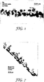
- FIG. 1 is an electron micrograph of the coated film of Example 3.
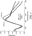
- FIG. 2 is the absorbance spectra of Example 2.
- FIG. 3 is the absorbance spectra of Example 3.
- FIG. 4 is the absorbance spectra of Example 4.
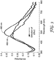
- FIG. 5 is the transmission spectra of Example 5.
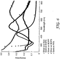
- FIG. 6 are the absorbance spectra of Example 1.
- FIG. 7 is an electron micrograph of the gold nanoparticle coated PFA (tetrafluoroethylene-perfluoromethyl vinyl ethyl copolymer) film of Example 1.
- the present invention is directed to methods of forming a nanoparticle coating on an stretched thermoplastic polymer film.
- the methods include providing a thermoplastic polymer film, onto which is deposited a discontinuous coating of metallic nanoparticles of an average size less than 100 nm by physical vapor deposition.
- the coated film may be further stretched or shrunk to shift the absorbance peak maximum to the desired degree.
- thermoplastic polymer film substrate An article comprising a thermoplastic polymer film substrate and a discontinuous metallic nanoparticle coating on the thermoplastic polymer film is obtained.
- the coating is formed by depositing a discontinuous layer of metallic nanoparticles by a physical vapor deposition method.
- the majority of the metal nanoparticles are usually elemental metal nanoparticles, although other metallic nanoparticles such as oxides are also contemplated.
- discontinuous means the nanoparticle coating is disposed as islands of nanoparticles or agglomerates thereof, surrounded by uncoated areas, such that the coating exhibits surface plasmon resonance. Continuous coatings, regardless of thickness, do not yield surface plasmon resonance.
- the present method provides a metallic nanoparticle coating on a thermoplastic polymeric film, the nanoparticles having a mean number average particle diameter in the range of 1 to 100 nanometers and most preferably 1 to 50 nanometers.
- the coating generally has an average thickness of less than 100nm, preferably less than 10 nm.
- the nanoparticles may be substantially spherical, but in some cases are elongated, having an aspect ratio (length to diameter) of greater than 1.5:1 (i.e. are substantially oblong).
- the film is stretched (oriented) prior to deposition, and may subsequently be further stretched or shrunk to shift the absorbance peak maximum to the desired degree.
- Average thickness of the nanoparticle coating may be measured during deposition using a commercially available quartz crystal microbalance. After deposition a number of chemical assays can be used to characterize the quantity of metal in any specified area. Particle diameter (formed by agglomeration of the nanoparticles) is typically measured using light scattering techniques known in the art. Primary particle diameter is typically measured using transmission electron microscopy or atomic force microscopy.
- the coated article allows the optical properties to by varied by stretching or shrinking. As the article is stretched or shrunk, the absorbance spectrum maximum is shifted to shorter or longer wavelengths respectively, so the optical properties may be varied as desired. In optical filter applications, this enables one to adjust the absorbance to a preselected maximum, so as to most efficiently filter out undesired wavelengths such as UV or IR wavelengths. In sensor applications, it allows one to match the absorbance peak maximum to a particular analyte and thereby maximize the response signal.
- the nanoparticles are prepared by physical vapor deposition techniques that generate the nanoparticles.
- Metal is heated under reduced pressure until vaporization occurs.
- the metal vaporizes in the presence of a gas stream wherein the gas preferably is inert (nonreactive), although any gas that does not react with the metal may be used.
- the nanoparticles are transported or directed to a polymeric film (optionally by the gas stream) and deposited by impinging the metallic vapor onto the film, wherein nucleation and nanoparticle growth occurs.
- the physical vapor deposition technique produces a metallic vapor than directly nucleates on the thermoplastic film surface.
- the metallic vapor undergoes some degree of homogenous nucleation in the stream to produce the nanoparticles, which are deposited on the film surface.
- the coating may be prepared by a method comprising the steps:
- the deposition of the metallic nanoparticles on the thermoplastic polymeric film may be achieved using one of several physical vapor deposition techniques known to those of ordinary skill in the art. Such processes include vapor deposition, cathode sputtering, pyrolysis, ion plating and e-beam deposition. Vapor deposition and cathode sputtering are often preferred in view of the uniformity of structure and thickness that can be obtained. Reference is made to Vacuum Deposition of Thin Films, L. Holland, 1970, Chapman and Hall, Lond on, England with regard to the many available means of providing metal vapors and vapor coating techniques. If desired, the nanoparticle layer may be pattern coated by means of a mask, so that the metallic nanoparticle surface may be patterned.
- PVD processes involve the deposition of atoms, typically by evaporation or sputtering in a vacuum.
- PVD processes can be characterized by the steps of (1) generating a metallic vapor by evaporation or sputtering using resistance, induction, electron-beam heating, laser-beam ablation, direct current plasma generation, radio-frequency plasma generation, molecular beam epitaxy, or similar means; (2) transport of the metallic vapor from the source to the substrate by molecular flow, viscous flow or plasma gas transport; and (3) nanoparticle growth on the thermoplastic polymer film, wherein nucleation and growth of the nanoparticles occurs.
- substrate temperatures can be used to control the crystallization and growth mode of the material deposited, although generally the temperature of the thermoplastic polymer film is below the distortion temperature of the polymer.
- the film is generally maintained at a temperature at or below the distortion temperature of the polymer.
- the integrity of the film is maintained by controlling the deposition rate so that the temperature of the nanoparticles, or the heat released by the nanoparticles upon deposition (heat of condensation) does not lead to thermal deformation of the film.
- the temperature of the film is maintained at ambient conditions of the deposition chamber, and no special cooling of the film is required.
- the nanoparticle coatings are applied to the thermoplastic polymer film by electron beam evaporation.
- This technique is based on heat production by high-energy electron beam bombardment on the metal to be deposited.
- the electron beam is generated by an electron gun, which uses the thermionic emission of electrons produced by an incandescent filament (cathode). Emitted electrons are accelerated towards an anode by a high difference of potential (kilovolts).
- the crucible (containing the source metal) itself or a near perforated disc can act as the anode.
- a magnetic field is often applied to bend the electron trajectory, allowing the electron gun to be positioned below the evaporation line.
- Physical vapor deposition by sputtering is accomplished in a partial vacuum (between 13.3 to 1.33 Pa for a diode system and between 1.3 to 0.13 Pa for a magnetron system) when the target (usually a cathode) is bombarded with gas ions propelled by an electric field.
- the sputtering gas is typically a noble gas such as argon but the sputtering gas could include reactive elements that can be incorporated into the deposited film such as the deposition of nitrides, oxides and carbides.
- a glow discharge or plasma is produced.
- the gas ions are accelerated towards the target by an electric or electric and magnetic fields. Atoms from the target are ejected by momentum transfer and move across the vacuum chamber to be deposited on the substrate (the thermoplastic polymer film).
- the nanoparticle coatings are applied to the thermoplastic polymer film by sputter deposition.
- the sputtering apparatus generally consists of a three-source magnetron sputtering system arranged around the outer circumference of a cylindrical chamber containing a 38 cm (15 inch) diameter rotating drum.
- the substrates are mounted on the drum and rotated sequentially past positions in front of the sputtering sources at rates of between 1 and 8 rpm.
- the sources are shielded such that the sample is not coated from any two fluxes at the same time.
- the rate of material deposition and speed of rotation of the substrate in front of the targets determines the individual layer thicknesses comprising the final catalyst particles. Any vacuum pump that can draw a sufficient vacuum may be used.
- cryopump Varian Associates, Lexington, Mass.
- Alcatel 2012A rotary vane-roughing pump Alcatel Vacuum Products, Hingham, Mass.
- the cryopump may be partially isolated from the chamber by a butterfly valve.
- deposition pressure may be maintained at 0.28 Pa (2.1 millitorr) as the sputtering gas flow rate was controlled by MKS flow controllers (MKS Instruments Inc., Andover, Mass.).
- Any inert or reactive sputtering gases may be used.
- argon or an argon oxygen mix is used. Control of the oxygen stoichiometry can be achieved by varying the argon/oxygen flow ratio.
- Any appropriate targets and power sources may be used.
- an Advanced Energy MDX 500 power supply Advanced Energy Industries, Inc., Fort Collins, Colo.
- Useful metals that may be used in the physical vapor deposition step include, for example, Li, Na, K, Rb, Cs, Fr, Be, Mg, Ca, Sr, Ba, Ra, Y, La, Ac, Ti, Zr, Hf, V, Nb, Ta, Cr, Mo, W, Mn, Tc, Re, Fe, Ru, Os, Co, Rh, Ir, Ni, Pd, Pt, Cu, Ag, Au, Zn, Cd, Al, In, Tl, Sn, Pb, mixtures, oxides and alloys of these metals and even the lanthanides and actinides, if desired. Metals may be deposited sequentially or simultaneously.
- Particularly useful metals are gold, aluminum, copper, iron, platinum, palladium, iridium, rhodium, osmium, ruthenium, titanium, cobalt, vanadium, magnesium, silver, zinc, and cadmium, indium, lanthanum, indium tin oxide (ITO) and antimony tin oxide (ATO), antimony indium tin oxide (AITO), tin, indium, lanthanum, boron, lanthanum hexaboride, rare earth metals and mixtures and alloys thereof, and mixtures and alloys thereof. Most preferred are the noble metals. Other metals are apparent to those skilled in the art.
- the process may involve evaporation of the elemental metal itself, as with Au or Ag, or may involve evaporation of a precursor form with generation of the actual elemental metal taking place during the transport stage prior to contacting the polymeric film.
- An example would be evaporation of silver metal using argon as a nonreactive gas with subsequent exposure of the silver nanoparticles to a reactive oxygen environment, thereby forming ultrafine silver oxide coated nanoparticles (the particle core being silver) prior to contacting the polymeric film.
- the final nanoparticles consist of a central core and an outer shell, where the central core can be metal and where the outer shell can be comprised of a layer formed by reaction of the reactive gas with the metal nanoparticles.
- the inert gas is generally selected from He, Ne, Ar, Xe, and N 2 . Mixtures of two or more nonreactive gases can also be used.
- a reactive gas can be introduced through a gas inlet that is positioned so as to minimize reaction with the bulk material in the crucible and allow thorough mixing of the reactive gas with the particles entrained in the gas stream, thereby allowing reaction with the particles to occur.
- the reactive and nonreactive gases generally are at room temperature but the temperature can be elevated or reduced as desired.
- the term reactive includes 1) direct reaction with the particles, as in the case of metals, for example, with O 2 , NO, NO 2 , CO 2 , CO, AsH 3 , H 2 S, H 2 Se, NH 3 , trimethylchlorosilane, methylamine, ethylene oxide, water, HF, HCl, or SO 2 , or combinations thereof, to form the corresponding oxides or other compounds; or 2) adsorption, in which a volatile substance is introduced in the gas prior to contacting the dispersing medium, but the substance is either not a liquid under normal conditions (atmospheric pressure and 25° C), the substance is not miscible with the dispersing medium, or else the substance acts to protect the surface of the nanoparticles from the dispersing medium or additives within the dispersing medium.
- Typical substances that could be adsorbed include polymers such as poly(methylmethacrylate) and polystyrene.
- a useful apparatus for coating of the nanoparticles comprises:
- reactor designs to provide dispersions can be envisioned, including a rotary metal atom reactor such as described in Metal Vapour Synthesis in Organometallic Chemistry, J. R. Blackborow and D. Young, Springer-Verlag (New York), 1979 and a spinning disk assembly such as described in Jpn. J. Appl. Phys., 13, 749 (1974 ). Both types of reactors could be used to generate dispersions of organic pigments.
- resistive heating other means of applying heat to the pigment or pigment precursor may be envisioned. These include laser heating, inductive heating, plasma jet, plasma arc discharge, and others known to those skilled in the art.
- nanoparticles exhibit useful optical properties as demonstrated by the tunable or controllable absorbance spectra.
- thermoplastic polymers for use in the film include polyesters, polyolefins and polystyrene. Processes for preparing the thermoplastic polymers are well known, and the invention is not limited to a polymer made with a particular catalyst or process.
- the thermoplastic polymer film may be a single or multi-layer polymer film.
- preferred thermoplastic polymers are poly(alpha)olefins.
- Poly(alpha)olefins can include the homo-, co- and terpolymers of aliphatic mono-alpha-olefins as they are generally recognized in the art.
- the monomers employed in making such poly(alpha)olefins contain about 2 to 10 carbon atoms per molecule, though higher molecular weight monomers sometimes are used as comonomers.
- the invention is applicable also to blends of the polymers and copolymers prepared mechanically or in situ.
- thermoplastic polymers examples include ethylene, propylene, 1-butene, 1-pentene, 4-methyl-1-pentene, 1-hexene, and 1-octene, alone, or in admixture, or in sequential polymerization systems.
- preferred thermoplastic polymers include polyethylene, polypropylene, propylene/ethylene copolymers, polybutylene and blends thereof.
- any polyester-containing polymer may be preferred.
- Useful polyester polymers include polymers having terephthalate or naphthalate comonomer units, for example, polyethylene naphthalate (PEN), polyethylene terephthalate (PET) and copolymers and blends thereof. Examples of other suitable polyester copolymers are provided in, for example, U.S. patents 6,827,886 , 6,808,658 , 6,830,713 and 6,783,349 .
- polyester materials include polycarbonates, polyarylates, and other naphthalate and terephthalate-containing polymers, such as, for example, polybutylene naphthalate (PBN), polypropylene naphtahalate (PPN), and blends and copolymers of the above with each other or with non-polyester polymers.
- PBN polybutylene naphthalate
- PPN polypropylene naphtahalate
- the thermoplastic polymer film contain substantially no particulate additives such as pigments, fillers, reinforcing agents.
- additives when present, can adversely affect the absorbance, alter the dielectric properties of the thermoplastic film and increase light scattering.
- such additives if present, are less than 1 wt. % of the thermoplastic polymer film.
- the nanoparticle-coated article may further comprise a dye or pigment for sensitizing the metallic nanoparticles to a particular wavelength of incident light.
- a dye or pigment for sensitizing the metallic nanoparticles may be coated on the nanoparticle-coated article before or after stretching, rather than be embedded or dispersed in the polymer matrix.
- Such sensitizers are normally used at less than 1 weight percent, relative to the weight of the metallic nanoparticles.
- thermoplastic polymer film may be stretched before or after deposition of the metallic nanoparticles. It will be understood however that whether the film is stretched or unstretched prior to nanoparticle deposition, the coated film may be subsequently stretched (or shrunk) to provide the desired absorption spectrum. Thus a stretched film may be coated with nanoparticles, and then further stretched, or preferably an unstretched film is coated with nanoparticles, then stretched. Generally the stretch imparts a permanent deformation to the thermoplastic film so that the dimensions (length and/or width) are increased, although permanent deformation is not required for the desired effect.
- the stretching increases (or shrinking decreases) the interparticle distance and shifts the absorbance peak maximum (to shorter or longer wavelengths respectively).
- this enables one to adjust the absorbance to a preselected maximum, so as to most efficiently filter out undesired wavelengths such as UV or IR wavelengths.
- it allows one to match the absorbance peak maximum to a particular analyte and thereby maximize the response signal.
- the film is stretched (or shrunk) in an amount sufficient to shift the absorbance peak maximum of the coated article at least 10 nm, preferably at least 20 nm.
- the polymer film may be stretched along one major axis (uniaxial), and may further be stretched along two major axes (biaxial).
- the stretching may be sequential or simultaneous.
- the degree of stretching is generally defined by the draw ratio, that is, the ratio of the final area to the original area. This stretching may be effected by a combination of techniques in the present invention, including the steps of calendering and length stretching.
- the total draw ratio is at least 5 X.
- the conditions for stretching are chosen such that the desired shift in the absorption peak maximum is achieved and the integrity of the film is maintained.
- the temperature is chosen such that substantial tearing, distortion or fragmentation of the film is avoided and integrity is maintained.
- the film may be vulnerable to tearing or even catastrophic failure if the temperature is too low, or the stretching ratio(s) is/are excessively high.
- the stretching temperature is above the glass transition temperature of the polymer. Such temperature conditions permit stretching in the X and Y directions without loss of film integrity.
- the core polymeric body When stretched, the core polymeric body may also be allowed to dimensionally relax in the cross-stretch direction from the natural reduction in cross-stretch (equal to the square root of the stretch ratio) or may also be constrained (i.e., no substantial change in cross-stretch dimensions).
- the core film may be stretched in the machine direction, as with a length orienter, and in the width direction using a tenter, or at diagonal angles.
- pre-stretch temperature, stretch temperature, stretch rate, stretch ratio, heat set temperature, heat set time, heat set relaxation, and cross-stretch relaxation are selected to yield a film having desired properties, including a desired refractive index relationship.
- the stretching of the nanoparticle coated article is not equal in the transverse and longitudinal directions of the film, the article will exhibit different optical properties along the two major axes. This may result from uniaxial stretching, or from unequal biaxial stretching, where the stretching along one axis is greater than stretching along the other. It is preferred that the stretching is biaxial, and substantially equal on both axes, i.e. stretching along one axis is within 20% of stretching along the other axis.
- the coated article may be annealed, preferably after stretching at a sufficient temperature to relieve stress but not so long or at so high a temperature that degradation of the film results. Suitable annealing temperatures vary with the type of polymer used. Preferably no pressure is applied to the film during the annealing step, only heat, although slight pressure less than about 10 psi is not detrimental. Ordinarily the film to be annealed is merely laid on a non-adherent support around which hot air is circulated or over which radiant heaters are placed.
- the method may also comprise a step of shrinking the nanoparticle-coated film. Upon shrinking, the interparticle distance is reduced, and the absorbance peak maximum is shifted to longer wavelengths. In optical filter applications, this enables one to adjust the absorbance to a preselected maximum, so as to most efficiently filter out undesired wavelengths such as UV or IR wavelengths. In sensor applications, it allows one to match the absorbance peak maximum to a particular analyte and thereby maximize the response signal.
- a shrinkable polymeric film having a discontinuous metallic nanoparticle coating onto a portion of the polymeric film.
- the temperature of the shrinkable, coated polymeric film is elevated such that the projected surface area of the polymeric film shrinks by an amount sufficient that the absorbance peak maximum is shifted by at least 10 nm, preferably at least 20 nm.
- the step of shrinking comprises exposing the shrinkable coated article to an elevated temperature for a time sufficient such that the article shrinks to less than 50 percent of its original projected surface area, sometimes less than 10 percent of its original projected surface area, and in certain embodiments less than 5 percent of its original projected surface area.
- the shrinkable film may be held in a tenter apparatus, or between two planar surfaces, during the heat shrinking.
- the nanoparticle-coated film is shrunk to provide the desired shift in the absorption spectrum. It should be recognized that excessive shrinking may lead to continuity between the previously discontinuous nanoparticles (and agglomerates), with an increase in electrical conductivity, reflection, and a loss or reduction in the surface plasmon resonance.
- the nanoparticle coated polymeric shrink film substrate is typically shrunk using a heat source, such as by convection or contact heating. Also, in some implementations the heating process may be performed by microwave, radio frequency or infrared radiation.
- the article may further comprise a protective layer for isolating the nanoparticles from environmental effects and mechanical stresses.
- the additional layer may be in contact with the metallic nanoparticle layer and the exposed surface of the thermoplastic film layer (i.e. the uncoated regions). This layer can act to reduce the surface roughness of both the polymeric layer and the overall construction, maintain the clarity and low haze of the article, and protect the nanoparticle layer from abrasion or oxidation.
- the protective layer may also be used to impart scratch resistance, chemical resistance and/or increased weatherability.
- the protective layer can be coextruded onto the surfaces of the coated surface of the thermoplastic film layer. Alternatively, the protective layer can be coated or laminated onto the thermoplastic film layer using a suitable pressure sensitive or non-pressure sensitive adhesive.
- Suitable coatings include, but are not limited to, hardcoats, adhesives, antistatics, adhesion promoting primers, UV stabilizing coating, friction reduction layers, etc.
- the protective layers are preferably made of a transparent polymer, for example, polyester (the same or different as that used in the construction of the thermoplastic polymer film layer.
- the resulting article may be characterized as a stretchable or shrinkable film having a discontinuous coating of nanoparticles or agglomerates of nanoparticles on the surface thereof and that the article exhibits a surface plasmon resonance.
- the maximum average thickness of the coating is less than 100 nm, preferably less than 10 nm with areas of nanoparticles or agglomerates thereof and uncoated areas. Above approximately 100 nm the coating tends of behave as a continuous metalized film, which do not exhibit a surface plasmon resonance.
- a multilayer article comprised a plurality of nanoparticle coated films may be used. The films may be bonded or otherwise affixed to adjacent layers, or may comprise a stack of nanoparticle coated films.
- the multilayer articles increase the total absorbance (an additivity of absorbance) while maintaining the surface plasmon resonances, which is generally not possible by increasing the nanoparticle coating thickness.
- the multilayer article further shows an internal reflectance between layers, which results in an interference fringe.
- the particles are partially fixed on the surface of the thermoplastic film and exposed, rather than embedded therein. Electron micrographs of a cross section of the coated article indicate the nanoparticles are substantially above the plane of the film. Generally more than 50%, typically more than 75% of the volume of the nanoparticles are above the surface. The particles remain fixed on the surface and are not easily removed. Typically less than 5% of the particles are removed by a tape test in which adhesive tape is affixed to the surface, and then peeled off at 180 degrees.
- the nanoparticle coating avoids contamination of dispersed material due to the presence of milling media and the wear of mechanical parts; these problems having been noted above for dispersions prepared by conventional methods employing mechanical grinding of particulates. Additionally, no chemical reduction process is required in order to achieve the fine particle sizes obtained in the final coating; the solvents and reducing agents employed may contaminate the nanoparticles.
- the absorption peak maximum of the coated article is a function of the metal or metallic compound deposited, the average thickness, the average particle size and shape (including agglomerates), the polymer used as the substrate and the degree of stretching (or shrinkage) of the article.
- the absorption spectrum broadens and the maximum shifts to longer wavelengths.
- Electron micrographs reveal that as the mass thickness increases, the average particle size increases and the space (uncoated areas) between nanoparticles decreases as result of agglomeration.
- the average thickness may be controlled by the deposition rate and the time of deposition (the time the film is exposed to the metallic vapor).
- the surface plasmon resonance and the absorption spectrum may be measured by spectrophotometry.
- the surface plasmon absorption spectrum of the metallic material may be measured by any suitable means for detection of transmitted light.
- suitable means include UV-vis spectrophotometers, such as those available commercially from companies such as Beckman Coulter (DU Series 500 Scanning Spectrophotometers and DU Series 600 High Performance Spectrophotometers), Spectral Instruments (400 Series spectrometers), Varian Instruments (Cary 300Bio spectrophotometer), Safas Monaco (UVmc series spectrophotometers and D.E.S.
- spectrophotometers include CCD cameras and flatbed optical scanners, which are also commercially available, such as a UMAX super vista S-12 flatbed scanner (UMAX Technologies, Inc.), preferably in combination with means for converting the image to grey scale and/or means for determining the density of an image, such as Scion Image software (Scion Corp).
- UMAX super vista S-12 flatbed scanner UMAX Technologies, Inc.
- the nanoparticle-coated article may be used as a sensor in analytical applications.
- the sensor comprises the nanoparticle coated thermoplastic film, and a binding agent disposed over at least a portion of the nanoparticle coating.
- the binding agent interacts with a predetermined substance present in the biological, biochemical, chemical or environmental solution being tested with the sensor.
- a predetermined substance present in the biological, biochemical, chemical or environmental solution being tested with the sensor.
- Any suitable reactive substance may be employed in the present invention, provided that it does not deleteriously affect either the metallic material or the optically transparent substrate.
- the binding agent is an agent involved in biological binding with at least one predetermined substance present in the biological, biochemical, chemical or environmental sample being tested.
- biological binding is intended to mean the interaction between a corresponding pair of molecules that exhibit mutual affinity or binding capacity, typically specific or non-specific binding or interaction, including biochemical, physiological and/or pharmaceutical interactions, such as pairs of proteins, nucleic acids, glycoproteins, carbohydrates, hormones and the like.
- Illustrative examples of such corresponding pairs or molecules include, but are not limited to, the following: antibody/antigen; antibody/hapten; enzyme/substrate; enzyme/cofactor; enzyme/inhibitor; binding protein/substrate; carrier protein/substrate; lectin/carbohydrate; receptor/hormone; receptor/effector; nucleic acid strand/complementary nucleic acid strand; protein/nucleic acid repressor or inducer; ligand/cell surface receptor; and virus/ligand.
- a functionalized material may be used to improve the adherence of the binding agent to the metallic nanoparticles and/or thermoplastic film layer. Accordingly, any material that adheres to both the metallic material and/or thermoplastic film layer, and the binding agent, but is not deleterious to either, may be employed as the second functionalized material.
- Suitable compounds for use as the second functionalized material are known to those skilled in the art and include, for example, organic compounds containing one or more of the functional groups including phosphonic acids, benzotriazoles, azlactones, -COOH, -CN, -NH 2 , 2-pyridyl, -P(C 6 H 5 ) 2 and/or -SH.
- Particularly preferred examples of a second functionalized material are carboxyl-terminated organothiols, such as 3-mercaptopropionic acid.
- a particular functionalized material to be employed in such an embodiment of the present invention will therefore depend, at least in part, upon the particular metallic material and specific reactive substance employed. Accordingly, the choice of a particular second functionalized material may be determined empirically by one skilled in the art, in view of the particular metallic material and reactive substance being used.
- thermoplastic film layer be substantially transparent.
- substantially transparent is intended to mean a substance that permits transmission of at least 50% of the light in the ultraviolet region (about 200 to about 400 nm), visible region (about 400 to about 750 nm), or infrared (greater than about 750 nm) of the spectrum.
- the sensor(s) are preferably employed in combination with a means for detection of transmitted light in the ultraviolet region (about 200 to about 400 nm), visible region (about 400 to about 750 nm) and/or infrared region (greater than about 750 nm) of the spectrum.
- a means for detection of transmitted light in the ultraviolet region (about 200 to about 400 nm), visible region (about 400 to about 750 nm) and/or infrared region (greater than about 750 nm) of the spectrum.
- Commercially available examples of such means for detection of transmitted light include, but are not limited to, UV-vis spectrophotometers, infrared spectrometers and flatbed optical scanners.
- One preferred embodiment invention is directed to a plurality of the sensors arranged in an array format.
- an array of sensors is preferably employed in combination with a means for detection of transmitted light in the ultraviolet region (about 200 to about 400 nm) and/or visible region (about 400 to about 750 nm), such as a flatbed optical scanner or CCD camera, or the infrared region of the spectrum (greater than about 750 nm).
- a means for detection of transmitted light in the ultraviolet region (about 200 to about 400 nm) and/or visible region (about 400 to about 750 nm) such as a flatbed optical scanner or CCD camera, or the infrared region of the spectrum (greater than about 750 nm).
- Such an embodiment is particularly useful for use in an endpoint-assay or as a screening tool in combinatorial chemistry, proteomics and/or genomics.
- An optical element is provided for selective absorption and transmission of incident light, including polarized light.
- the absorption spectrum of the nanoparticle-coated article may be controlled by appropriate stretching or shrinking of the article.
- the optical film can be used in any application to provide selective absorption, transmission and reflection.
- the optical film can incorporate or be applied to other optical bodies or films to combine multiple optical effects.
- the optical bodies can be incorporated along with one or more additional optically active layers to form an IR mirror, UV absorption construction, solar control construction, polarizer, or decorative construction.
- the optical element can be used to provide optical filters to window glazing, and lenses made of glass or polycarbonates.
- the optical element may also find application in the construction of puncture-or tear-resistant films, safety and security films, and as contrast enhancement layers for optical displays, for example, computer monitors, television screens, and the like.
- Metallic nanoparticles were e-beam evaporated onto various films as follows: silver on biaxially oriented polystyrene (BOPS, refractive index of approximately 1.6), silver on biaxially oriented polypropylene (BOPP, refractive index of approximately 1.5), silver, then gold on biaxially oriented polypropylene (BOPP, refractive index of approximately 1.5), and gold on PFA (a copolymer of tetrafluoroethylene and perfluoromethylvinylether, available from Dyneon, St. Paul, MN, refractive index of approximately 1.35).
- BOPS biaxially oriented polystyrene
- BOPP biaxially oriented polypropylene
- PFA a copolymer of tetrafluoroethylene and perfluoromethylvinylether
- nanoparticle samples were made at an e-beam deposition rate of 20 nm/s (2 ⁇ /s) ( ⁇ ngstrom/second) to yield a nominal average thickness of approximately 400 nm (40 ⁇ ).
- This example shows the effect of changing the refractive index of the substrate (compare Ag on PP vs Ag on PS) and the effect of sequentially coating two different metals (Au and Ag on PP).
- the films yielded different colors; the gold on PFA was a blue to light grey color, the silver on BOPS was a purple, and the silver on BOPP was amber yellow.
- the spectra showing the nanoparticle resonances of the coated articles are shown in Figure 6.
- Figure 6 also shows the shift in peak maxima obtained when a different refractive index substrate was utilized and also shows the effect of a sequential deposition of silver and then gold nanoparticles on a BOPP substrate.
- Silver nanoparticles were e-beam evaporated onto biaxially oriented polypropylene (BOPP) film to yield a 600 nm (60- ⁇ ) coating.
- the coated BOPP film had a yellowish/amber tint.
- Samples of the coated film were stretched in an Instron tensile testing machine (Model 1122 from Instron Corp.; Canton, MA) with a temperature conditioning chamber set at 100°C and a stretching rate of 0.25 centimeters per minute (0.1 inches per minute).
- UV-Vis spectra were taken as described in Example 1 of the unstretched film, the film was stretched to 50% strain in 2 orthogonal directions, and the film stretched to 100% strain in one direction. The spectra are shown in Figure 2 .
- the absorbance spectra reveal a second maximum, or shoulder, at approximately 540 to 580 nm as result of the orientation.
- the nanoparticle spacing in the direction of orientation becomes greater, and the absorbance peak maximum is shifted to shorter wavelengths.
- the nanoparticle distance in the direction perpendicular to the direction of orientation becomes smaller, and a new absorbance peak at higher wavelengths develops.
- Silver nanoparticles were e-beam evaporated onto BOPS film to yield a 60 Angstrom coating.
- the coated BOPS film had a purple tint.
- Samples of the coated film were stretched in an Instron tensile testing machine (Model 1122 from Instron Corp.; Canton, MA) with a temperature conditioning chamber set at 100°C and a stretching rate of 0.25 centimeters per minute (0.1 inches per minute).
- UV Vis spectra were taken as described in Example 1 of the unstretched film, the film, stretched to 50% strain in 2 orthogonal directions, and the film stretched to 150% strain in one direction.
- a cross section of the coated film is shown in Figure 1 .
- the spectra are shown in Figure 3 , which again reveals a shift to shorter wavelengths as result of orientation, and a new absorbance peak at approximately 600 nm as result of decreased nanoparticle spacing in the direction perpendicular to orientation.
- Silver nanoparticles were e-beam evaporated onto BOPS Film as described in Example 3.
- a sample of the coated film was shrunk in an oven set at 140°C for 5 minutes.
- the resulting film was had an overall shrinkage of approximately 20%.
- UV Vis spectra were taken as described in Example 1 of the unshrunk film and the shrunken film. The spectra are shown in Figure 4 , which reveals the absorbance peak maximum shifter to longer wavelengths as result of shrinking.
- Silver nanoparticles were e-beam evaporated onto biaxially oriented polypropylene film in the presence of oxygen to yield silver oxide (AgO surface with Ag core) nanoparticle coatings of 800 nm (80 ⁇ ) (Sample 5A), 1200 nm (120 ⁇ ) (Sample 5B), 2000 nm (200 ⁇ ) (Sample 5C).
- the coated BOPP films 5A and 5B had a yellowish/amber tint while 5C had a brownish tint.
- the coated films were tested for surface conductivity with a Fluke 27 multimeter (John Fluke Mfc. Co. Inc, Everett, Washington) but showed no surface conductivity.
- Sample 5C was placed in a 160°C oven and shrunk by 20% and retested with multimeter and showed a resistance of 13 Kilo-Ohms when point probes were placed 1 cm apart on the surface of the specimen. This measurement was done at room temperature and approximately 30% relative humidity. The shrunken sample had a brown/gray appearance and an average of 30% transmission in the visible range.
- the transmission spectra showing the nanoparticle resonances of the initial materials is shown in Figure 5 .
- the plasmon absorption is observed in the 80 Angstrom sample and it is less evident in samples with low transmission as the nominal coating thickness increases.
- the measurements shown in this example denote the transition from a coating that is conductive and fully reflective to a non-conductive plasmonic absorptive coating.
- Spectra were taken using a Perkin Elmer Lamda 19 Spectrometer. Scanned at 5 nm intervals from 300-2500 nm (6 minutes per scan).
Landscapes
- Health & Medical Sciences (AREA)
- Chemical & Material Sciences (AREA)
- Engineering & Computer Science (AREA)
- Life Sciences & Earth Sciences (AREA)
- Immunology (AREA)
- Physics & Mathematics (AREA)
- Molecular Biology (AREA)
- General Physics & Mathematics (AREA)
- Biomedical Technology (AREA)
- Urology & Nephrology (AREA)
- Hematology (AREA)
- General Health & Medical Sciences (AREA)
- Nanotechnology (AREA)
- Biochemistry (AREA)
- Pathology (AREA)
- Analytical Chemistry (AREA)
- Medicinal Chemistry (AREA)
- Microbiology (AREA)
- Food Science & Technology (AREA)
- Biotechnology (AREA)
- Cell Biology (AREA)
- Materials Engineering (AREA)
- Optics & Photonics (AREA)
- Crystallography & Structural Chemistry (AREA)
- Metallurgy (AREA)
- Mechanical Engineering (AREA)
- Chemical Kinetics & Catalysis (AREA)
- Organic Chemistry (AREA)
- Laminated Bodies (AREA)
- Shaping By String And By Release Of Stress In Plastics And The Like (AREA)
- Investigating Or Analysing Materials By Optical Means (AREA)
Applications Claiming Priority (2)
| Application Number | Priority Date | Filing Date | Title |
|---|---|---|---|
| US11/073,787 US7274458B2 (en) | 2005-03-07 | 2005-03-07 | Thermoplastic film having metallic nanoparticle coating |
| PCT/US2006/002990 WO2006096255A2 (en) | 2005-03-07 | 2006-01-27 | Thermoplastic film having metallic nanoparticle coating |
Related Child Applications (1)
| Application Number | Title | Priority Date | Filing Date |
|---|---|---|---|
| EP11190602.0 Division-Into | 2011-11-24 |
Publications (2)
| Publication Number | Publication Date |
|---|---|
| EP1861693A2 EP1861693A2 (en) | 2007-12-05 |
| EP1861693B1 true EP1861693B1 (en) | 2012-05-16 |
Family
ID=36590145
Family Applications (1)
| Application Number | Title | Priority Date | Filing Date |
|---|---|---|---|
| EP06719715A Not-in-force EP1861693B1 (en) | 2005-03-07 | 2006-01-27 | Method for preparing a thermoplastic film having metallic nanoparticle coating |
Country Status (6)
| Country | Link |
|---|---|
| US (1) | US7274458B2 (enExample) |
| EP (1) | EP1861693B1 (enExample) |
| JP (1) | JP5319272B2 (enExample) |
| KR (1) | KR20070116859A (enExample) |
| CN (1) | CN101137898B (enExample) |
| WO (1) | WO2006096255A2 (enExample) |
Families Citing this family (65)
| Publication number | Priority date | Publication date | Assignee | Title |
|---|---|---|---|---|
| US7666494B2 (en) * | 2005-05-04 | 2010-02-23 | 3M Innovative Properties Company | Microporous article having metallic nanoparticle coating |
| US7935540B2 (en) * | 2005-07-14 | 2011-05-03 | 3M Innovative Properties Company | Water-soluble polymeric substrate having metallic nanoparticle coating |
| US7465497B2 (en) * | 2005-11-23 | 2008-12-16 | General Electric Company | High dielectric constant nanocomposites, methods of manufacture thereof, and articles comprising the same |
| EP2351610A3 (en) * | 2006-03-28 | 2011-10-12 | Inanovate, Inc. | Nano-particle biochip substrates |
| US7952805B2 (en) * | 2006-08-22 | 2011-05-31 | 3M Innovative Properties Company | Solar control film |
| GB2454132B (en) * | 2006-08-24 | 2011-11-23 | Ngimat Co | Optical coating |
| US7906223B2 (en) * | 2006-09-11 | 2011-03-15 | 3M Innovative Properties Company | Permeable nanoparticle reflector |
| KR100857590B1 (ko) * | 2007-02-12 | 2008-09-09 | 충남대학교산학협력단 | 연성 폴리머 기판 위에 상온 화학증착법 |
| US7609377B2 (en) * | 2007-04-26 | 2009-10-27 | Hewlett-Packard Development Company, L.P. | Surface enhanced raman spectroscopy with periodically deformed SERS-active structure |
| US8197901B2 (en) * | 2007-07-16 | 2012-06-12 | University Of Kentucky | In-situ nanoparticle formation in polymer clearcoats |
| AU2008321027A1 (en) * | 2007-11-13 | 2009-05-22 | The Regents Of The University Of California | Processes for rapid microfabrication using thermoplastics and devices thereof |
| WO2009068041A1 (en) * | 2007-11-29 | 2009-06-04 | Danmarks Tekniske Universitet | Three-dimensional optical structure |
| FR2924723B1 (fr) * | 2007-12-11 | 2010-12-17 | Centre Nat Rech Scient | Support solide revetu d'au moins un film de metal et d'au moins une couche d'oxyde transparent et conducteur pour la detection par spr et/ou par une methode electrochimique |
| DE102008033941A1 (de) * | 2008-07-18 | 2010-01-28 | Innovent E.V. | Verfahren zum Beschichten |
| DE102008033939A1 (de) | 2008-07-18 | 2010-01-21 | Innovent E.V. | Verfahren zur Beschichtung |
| US20100104652A1 (en) * | 2008-10-27 | 2010-04-29 | University Of Arkansas | Use of advanced nanomaterials for increasing sepecific cell functions |
| JP5099520B2 (ja) * | 2008-12-19 | 2012-12-19 | 独立行政法人産業技術総合研究所 | 貴金属粒子が基材表面に存在する物、積層体およびそれらの製造方法 |
| WO2010132610A2 (en) * | 2009-05-13 | 2010-11-18 | The Regents Of The University Of California | Thermoplastic substrates with wrinkled metallic surfaces for chemical and biological sensing |
| US8107070B2 (en) * | 2009-06-11 | 2012-01-31 | University Of Georgia Research Foundation, Inc. | Methods of melamine detection and quantification |
| EP3567416A1 (en) | 2009-10-12 | 2019-11-13 | The Trustees of Columbia University in the City of New York | Photonic crystal spectrometer |
| IT1399202B1 (it) * | 2010-03-30 | 2013-04-11 | Corbelli | Metodo per la produzione di manufatti elastomerici funzionalizzati e manufatti cosi' ottenuti |
| US10018831B2 (en) | 2010-03-30 | 2018-07-10 | Wise S.R.L. | Method for the production of stretchable and deformable optical elements, and elements thus obtained |
| JPWO2012070175A1 (ja) * | 2010-11-26 | 2014-05-19 | コニカミノルタ株式会社 | 分析チップのプリズム部、このプリズム部を含む分析チップ、及び分析チップのプリズム部の製造方法 |
| WO2012088117A1 (en) * | 2010-12-21 | 2012-06-28 | Ioannis Kymissis | Spectrometer including three-dimensional photonic crystal |
| US8810789B2 (en) | 2011-11-07 | 2014-08-19 | University Of Georgia Research Foundation, Inc. | Thin layer chromatography-surfaced enhanced Raman spectroscopy chips and methods of use |
| CN107815713B (zh) | 2012-06-22 | 2020-11-17 | 苹果公司 | 白色外观阳极化膜及其形成方法 |
| CA2787584A1 (en) | 2012-08-22 | 2014-02-22 | Hy-Power Nano Inc. | Method for continuous preparation of indium-tin coprecipitates and indium-tin-oxide nanopowders with substantially homogeneous indium/tin composition, controllable shape and particle size |
| US9493876B2 (en) * | 2012-09-14 | 2016-11-15 | Apple Inc. | Changing colors of materials |
| US9709349B2 (en) | 2012-11-15 | 2017-07-18 | The Board Of Trustees Of The Leland Stanford Junior University | Structures for radiative cooling |
| JP5737635B2 (ja) * | 2013-03-01 | 2015-06-17 | 大日本印刷株式会社 | 金属粒子が担持されたフィルムおよびフィルム製造方法 |
| CN103320753B (zh) * | 2013-06-21 | 2016-04-13 | 厦门大学 | 一种尺寸密度可控铝纳米颗粒阵列的制备方法 |
| US9181629B2 (en) | 2013-10-30 | 2015-11-10 | Apple Inc. | Methods for producing white appearing metal oxide films by positioning reflective particles prior to or during anodizing processes |
| US9839974B2 (en) | 2013-11-13 | 2017-12-12 | Apple Inc. | Forming white metal oxide films by oxide structure modification or subsurface cracking |
| ES2848062T3 (es) * | 2013-12-23 | 2021-08-05 | Illumina Inc | Sustratos estructurados para mejorar la detección de emisiones de luz y métodos relacionados con los mismos |
| ES2473216B1 (es) * | 2014-02-20 | 2015-06-02 | Universitat De Barcelona | Superficie con propiedades de reducción de la luz difusa por condensación de agua y procedimiento de obtención de esta |
| US10088251B2 (en) * | 2014-05-21 | 2018-10-02 | The Board Of Trustees Of The Leland Stanford Junior University | Radiative cooling with solar spectrum reflection |
| CN103984120B (zh) * | 2014-05-30 | 2015-06-10 | 奥特路(漳州)光学科技有限公司 | 一种防蓝光光学镜片的制造方法 |
| CU20170124A7 (es) * | 2014-07-08 | 2018-04-03 | Xyleco Inc | Método para identificar si un producto a base de plástico está marcado |
| US10656013B2 (en) | 2015-09-29 | 2020-05-19 | Chromation Inc. | Nanostructure based article, optical sensor and analytical instrument and method of forming same |
| FI129889B (en) * | 2015-10-09 | 2022-10-31 | Inkron Ltd | Dielectric siloxane particle films and devices containing them |
| WO2017165369A1 (en) * | 2016-03-21 | 2017-09-28 | Corning Incorporated | Transparent substrates comprising three-dimensional porous conductive graphene films and methods for making the same |
| WO2017197013A1 (en) | 2016-05-10 | 2017-11-16 | Chromation Inc. | Integration of optical components within a folded optical path |
| CN105951049B (zh) * | 2016-05-13 | 2018-04-13 | 中山大学 | 一种具有纳米级间隙的金属颗粒制造方法 |
| EP3554808A1 (en) * | 2016-12-19 | 2019-10-23 | 3M Innovative Properties Company | Flexible substrate having a plasmonic particle surface coating and method of making the same |
| CN107864604A (zh) * | 2017-11-10 | 2018-03-30 | 中国科学院西安光学精密机械研究所 | 一种电磁辐射屏蔽结构 |
| US11977207B2 (en) | 2018-03-15 | 2024-05-07 | The Regents Of The University Of California | Adaptive materials and systems for manipulation of electromagnetic radiation |
| US10620122B2 (en) * | 2018-04-05 | 2020-04-14 | Picoyune, Llc | Equilibrium plasmonic mercury sensing apparatus and methods |
| US20240159671A1 (en) * | 2018-04-05 | 2024-05-16 | Jay James | Equilibrium Plasmonic Analyte Sensing Apparatus and Methods |
| US11525945B2 (en) | 2018-06-22 | 2022-12-13 | Lawrence Livermore National Security, Llc | System and method for ablation assisted nanostructure formation for graded index surfaces for optics |
| KR102197549B1 (ko) * | 2018-07-16 | 2021-01-07 | 한국재료연구원 | 표면증강라만산란 패치 및 이를 이용한 부착형 센서 |
| KR20210096632A (ko) | 2018-11-27 | 2021-08-05 | 더 리젠츠 오브 더 유니버시티 오브 캘리포니아 | 조정 가능 스펙트럼 특성을 갖는 복합재 |
| WO2020140082A1 (en) | 2018-12-27 | 2020-07-02 | SkyCool Systems, Inc. | Cooling panel system |
| CN113906261A (zh) | 2019-04-17 | 2022-01-07 | 天酷系统股份有限公司 | 辐射冷却系统 |
| JP7307917B2 (ja) * | 2019-04-26 | 2023-07-13 | 国立大学法人群馬大学 | 生体高分子の濃縮化方法、結晶化方法およびナノ構造基板 |
| CN110835603A (zh) * | 2019-10-09 | 2020-02-25 | 遵义医科大学珠海校区 | 一种快速实现细胞膜可逆性损伤的装置及方法 |
| US12352464B2 (en) * | 2019-12-31 | 2025-07-08 | 3M Innovative Properties Company | Multi-surface passive cooling articles |
| WO2022076438A1 (en) | 2020-10-06 | 2022-04-14 | Chromation Inc. | Systems and methods to redistribute field of view in spectroscopy |
| US20240085592A1 (en) * | 2021-01-29 | 2024-03-14 | Opsec Security Group, Inc. | Method of creating a surface plasmon resonance |
| CN113459616B (zh) | 2021-06-24 | 2022-06-17 | 浙江大学 | 农产品、食品质量无损检测的包装材料、制备和检测方法 |
| CN115181949B (zh) * | 2022-07-07 | 2023-07-11 | 江苏理工学院 | 用于折射率传感的金银复合纳米颗粒薄膜及其制备方法 |
| KR102770480B1 (ko) | 2022-10-31 | 2025-02-20 | 계명대학교 산학협력단 | 극초음속 유동 대응이 가능한, 플라즈몬 나노입자를 활용한 나노입자 박막 제조방법 및 이에 의해 제조되는 플라즈몬 나노입자 박막 |
| KR102553980B1 (ko) * | 2022-11-16 | 2023-07-11 | 박준경 | 친환경 구리산화물 나노입자를 이용한 포름알데하이드 센서의 제조방법 |
| CN120359117A (zh) * | 2022-12-30 | 2025-07-22 | 杭州启明医疗器械股份有限公司 | 高分子瓣叶材料、瓣叶、瓣膜及其制备方法 |
| KR102840954B1 (ko) | 2023-01-31 | 2025-07-31 | 계명대학교 산학협력단 | 극초음속 비행체 소재에 적용 가능한 SiO2와 FITO의 다중박막층 및 그 제조방법 |
| KR20250059742A (ko) | 2023-10-25 | 2025-05-07 | 계명대학교 산학협력단 | 적외선을 차단하는 투명 필름 제조방법 및 이에 의해 제조되는 투명 필름 |
Citations (1)
| Publication number | Priority date | Publication date | Assignee | Title |
|---|---|---|---|---|
| WO2005012885A1 (de) * | 2003-07-31 | 2005-02-10 | Stiftung Caesar Center Of Advanced Studies And Research | Berührungsloser optischer dehnungssensor zur messung von änderungen in der partikel plasmonenresonanz |
Family Cites Families (78)
| Publication number | Priority date | Publication date | Assignee | Title |
|---|---|---|---|---|
| US4101698A (en) | 1975-07-14 | 1978-07-18 | Avery International Corp. | Elastomeric reflective metal surfaces |
| US4340276A (en) | 1978-11-01 | 1982-07-20 | Minnesota Mining And Manufacturing Company | Method of producing a microstructured surface and the article produced thereby |
| US4618525A (en) | 1985-06-03 | 1986-10-21 | Minnesota Mining And Manufacturing Company | Coated glass microbubbles and article incorporating them |
| US4871790A (en) | 1987-11-25 | 1989-10-03 | Minnesota Mining And Manufacturing Company | Colloidal metals in monomers or polymers |
| US5030669A (en) | 1988-05-27 | 1991-07-09 | Minnesota Mining And Manufacturing Company | Pigment dispersions |
| US5026599A (en) | 1988-08-29 | 1991-06-25 | Minnesota Mining & Manufacturing | Array of densely packed discrete metal microspheres coated on a substrate |
| US5238623A (en) | 1989-11-20 | 1993-08-24 | Minnesota Mining And Manufacturing Company | Method for preparing microporous polyolefin shaped articles |
| US5178726A (en) | 1991-03-07 | 1993-01-12 | Minnesota Mining And Manufacturing Company | Process for producing a patterned metal surface |
| US5330855A (en) | 1991-09-23 | 1994-07-19 | The United States Of America, As Represented By The Secretary Of Commerce | Planar epitaxial films of SnO2 |
| US6071621A (en) | 1993-06-11 | 2000-06-06 | 3M Innovative Properties Company | Metallized film and decorative articles made therewith |
| US5514728A (en) | 1993-07-23 | 1996-05-07 | Minnesota Mining And Manufacturing Company | Catalysts and initiators for polymerization |
| US5366140A (en) | 1993-09-30 | 1994-11-22 | Minnesota Mining And Manufacturing Company | Patterned array of uniform metal microbeads |
| AT403746B (de) | 1994-04-12 | 1998-05-25 | Avl Verbrennungskraft Messtech | Optochemischer sensor sowie verfahren zu seiner herstellung |
| US5472749A (en) | 1994-10-27 | 1995-12-05 | Northwestern University | Graphite encapsulated nanophase particles produced by a tungsten arc method |
| US6025202A (en) | 1995-02-09 | 2000-02-15 | The Penn State Research Foundation | Self-assembled metal colloid monolayers and detection methods therewith |
| US5976678A (en) | 1996-02-27 | 1999-11-02 | Nippon Sheet Glass Co., Ltd. | Colored film-covered glass articles |
| EP0902728A1 (en) | 1996-05-14 | 1999-03-24 | E.I. Du Pont De Nemours And Company | Catalyst compositions of nanoparticulate metal on a refractory support |
| US5774619A (en) * | 1996-05-15 | 1998-06-30 | Hughes Electronics Corporation | Precision deformation mechanism and method |
| US5750641A (en) | 1996-05-23 | 1998-05-12 | Minnesota Mining And Manufacturing Company | Polyimide angularity enhancement layer |
| US5736073A (en) | 1996-07-08 | 1998-04-07 | University Of Virginia Patent Foundation | Production of nanometer particles by directed vapor deposition of electron beam evaporant |
| US6538801B2 (en) * | 1996-07-19 | 2003-03-25 | E Ink Corporation | Electrophoretic displays using nanoparticles |
| WO1998010289A1 (en) | 1996-09-04 | 1998-03-12 | The Penn State Research Foundation | Self-assembled metal colloid monolayers |
| JPH10160737A (ja) * | 1996-12-03 | 1998-06-19 | Dainippon Printing Co Ltd | 光学的分析装置用測定チップ及びその製造方法 |
| US6344272B1 (en) | 1997-03-12 | 2002-02-05 | Wm. Marsh Rice University | Metal nanoshells |
| CA2294962C (en) | 1997-07-28 | 2012-09-18 | Medical Biosystems Ltd. | Nucleic acid sequence analysis |
| US5879827A (en) | 1997-10-10 | 1999-03-09 | Minnesota Mining And Manufacturing Company | Catalyst for membrane electrode assembly and method of making |
| US6808658B2 (en) | 1998-01-13 | 2004-10-26 | 3M Innovative Properties Company | Method for making texture multilayer optical films |
| JP3380744B2 (ja) * | 1998-05-19 | 2003-02-24 | 株式会社日立製作所 | センサおよびこれを利用した測定装置 |
| CA2338917A1 (en) | 1998-07-30 | 2000-02-10 | Minnesota Mining And Manufacturing Company | Nanosize metal oxide particles for producing transparent metal oxide colloids and ceramers |
| US6468657B1 (en) | 1998-12-04 | 2002-10-22 | The Regents Of The University Of California | Controllable ion-exchange membranes |
| US7057732B2 (en) | 1999-01-25 | 2006-06-06 | Amnis Corporation | Imaging platform for nanoparticle detection applied to SPR biomolecular interaction analysis |
| EP1212458A4 (en) | 1999-07-30 | 2005-01-05 | Surromed Inc | INSTRUMENTS, METHODS AND REAGENTS FOR PLASMON SURFACE RESONANCE |
| US6521324B1 (en) | 1999-11-30 | 2003-02-18 | 3M Innovative Properties Company | Thermal transfer of microstructured layers |
| JP3517698B2 (ja) | 2000-03-03 | 2004-04-12 | 独立行政法人産業技術総合研究所 | ナノ粒子分散構造体及びその積層体 |
| GB0006050D0 (en) | 2000-03-14 | 2000-05-03 | Johnson Matthey Plc | Liquid gold compositions |
| AU2001269473A1 (en) | 2000-07-07 | 2002-02-13 | Shizuko Sato | Ultrafine metal particle/polymer hybrid material |
| US6411748B1 (en) * | 2000-07-17 | 2002-06-25 | Alcatel Usa Sourcing, L.P. | Wide tuning range acousto-optical fiber Bragg grating filter (FBGF) |
| US6723388B2 (en) | 2000-07-28 | 2004-04-20 | Ekc Technology, Inc. | Method of depositing nanostructured films with embedded nanopores |
| AU2001278332A1 (en) | 2000-07-28 | 2002-02-13 | Simon Fraser University | Methods for the lithographic deposition of materials containingnanoparticles |
| CA2314398A1 (en) | 2000-08-10 | 2002-02-10 | Edward Shipwash | Microarrays and microsystems for amino acid analysis and protein sequencing |
| US7879598B2 (en) | 2000-09-04 | 2011-02-01 | Bayer Technology Services Gmbh | Multianalyte determination system and methods |
| US6773926B1 (en) * | 2000-09-25 | 2004-08-10 | California Institute Of Technology | Nanoparticle-based sensors for detecting analytes in fluids |
| US6569529B1 (en) * | 2000-10-10 | 2003-05-27 | Flex Product, Inc. | Titanium-containing interference pigments and foils with color shifting properties |
| AU2001272708A1 (en) | 2000-11-14 | 2002-05-27 | Cpfilms, Inc. | Optically active film composite |
| US6569517B1 (en) | 2000-11-17 | 2003-05-27 | 3M Innovative Properties Company | Color tailorable pigmented optical bodies with surface metalization |
| US20020142306A1 (en) | 2001-03-28 | 2002-10-03 | 3M Innovative Properties Company | Method of transferring molecules to a film laminate |
| US20030129545A1 (en) | 2001-06-29 | 2003-07-10 | Kik Pieter G | Method and apparatus for use of plasmon printing in near-field lithography |
| JP2003014765A (ja) * | 2001-07-02 | 2003-01-15 | Inst Of Physical & Chemical Res | センサーおよびそれを用いた物質の反応の検出方法 |
| CN1339339A (zh) * | 2001-07-12 | 2002-03-13 | 太原理工大学 | 纳米薄膜材料及其制备方法 |
| US7002697B2 (en) * | 2001-08-02 | 2006-02-21 | Aegis Semiconductor, Inc. | Tunable optical instruments |
| ATE528117T1 (de) | 2001-08-30 | 2011-10-15 | Bayer Technology Services Gmbh | Verfahren zur herstellung von abformkörpern, insbesondere optischen strukturen, und deren verwendung |
| US6778316B2 (en) | 2001-10-24 | 2004-08-17 | William Marsh Rice University | Nanoparticle-based all-optical sensors |
| US6962946B2 (en) * | 2001-11-21 | 2005-11-08 | 3M Innovative Properties Company | Nanoparticles having a rutile-like crystalline phase and method of preparing same |
| GR1004178B (el) | 2001-11-29 | 2003-03-05 | "����������" | Ολοκληρωμενος οπτοηλεκτρονικος βιοαισθητηρας πυριτιου για ανιχνευση βιομοριων επισημασμενων με χρωμοφορες ομαδες ή νανοσωματιδια |
| US6686308B2 (en) | 2001-12-03 | 2004-02-03 | 3M Innovative Properties Company | Supported nanoparticle catalyst |
| US7129096B2 (en) * | 2001-12-11 | 2006-10-31 | Duke University | Sensor for use in testing biological, biochemical, chemical or environmental samples |
| US6689192B1 (en) | 2001-12-13 | 2004-02-10 | The Regents Of The University Of California | Method for producing metallic nanoparticles |
| US6689190B2 (en) | 2001-12-20 | 2004-02-10 | Cima Nanotech, Inc. | Process for the manufacture of reacted nanoparticles |
| US6642295B2 (en) * | 2001-12-21 | 2003-11-04 | Eastman Kodak Company | Photoresist nanocomposite optical plastic article and method of making same |
| EP1471828A1 (en) | 2002-01-18 | 2004-11-03 | California Institute Of Technology | Method and apparatus for nanomagnetic manipulation and sensing |
| US20030145681A1 (en) | 2002-02-05 | 2003-08-07 | El-Shall M. Samy | Copper and/or zinc alloy nanopowders made by laser vaporization and condensation |
| WO2003093809A1 (en) | 2002-04-30 | 2003-11-13 | University Of Maryland, Baltimore | Fluorescence sensing |
| JP3837508B2 (ja) * | 2002-06-14 | 2006-10-25 | 独立行政法人産業技術総合研究所 | 表面プラズモン励起性貴金属微粒子状薄膜 |
| IL150325A (en) | 2002-06-19 | 2010-12-30 | Cima Nanotech Israel Ltd | Method for the production of highly pure metallic nano-powders and nano-powders produced thereby |
| US20040101454A1 (en) | 2002-09-05 | 2004-05-27 | Johnson D. Lynn | Supported metallic catalyst and method of making same |
| US7364673B2 (en) * | 2002-10-09 | 2008-04-29 | The Governing Council Of The University Of Toronto | Widely wavelength tuneable polychrome colloidal photonic crystal device |
| EP1579200A2 (en) * | 2002-10-28 | 2005-09-28 | University of Washington | Wavelength tunable surface plasmon resonance sensor |
| US7122384B2 (en) | 2002-11-06 | 2006-10-17 | E. I. Du Pont De Nemours And Company | Resonant light scattering microparticle methods |
| TWI245079B (en) | 2002-12-30 | 2005-12-11 | Ind Tech Res Inst | Method for growing highly-ordered nanofibers |
| US6838486B2 (en) * | 2003-01-07 | 2005-01-04 | Aps Laboratory | Preparation of metal nanoparticles and nanocomposites therefrom |
| JP3957199B2 (ja) * | 2003-03-19 | 2007-08-15 | 富士フイルム株式会社 | センサチップおよびセンサチップの製造方法並びにそのセンサチップを用いたセンサ |
| US20040157237A1 (en) | 2003-02-10 | 2004-08-12 | Americal Environmental Systems, Inc. | Optochemical sensing with multi-band fluorescence enhanced by surface plasmon resonance |
| DE10316379B4 (de) | 2003-04-10 | 2006-06-01 | Christian-Albrechts-Universität Zu Kiel | Verfahren zur Herstellung von Metall-Polymer-Nanokompositen |
| US20040253138A1 (en) | 2003-06-16 | 2004-12-16 | American Environmental Systems, Inc. | Plasmon enhanced body treatment and bacterial management |
| JP2005037905A (ja) * | 2003-06-30 | 2005-02-10 | Nitto Denko Corp | 高分子フィルム、偏光子、光学フィルムおよび画像表示装置 |
| GB0316553D0 (en) | 2003-07-15 | 2003-08-20 | Densham Daniel | Method |
| JP2005049297A (ja) * | 2003-07-31 | 2005-02-24 | National Institute Of Advanced Industrial & Technology | 光検出用バイオ素子とバイオ検出方法 |
| US20050136638A1 (en) | 2003-12-18 | 2005-06-23 | 3M Innovative Properties Company | Low temperature sintering nanoparticle compositions |
-
2005
- 2005-03-07 US US11/073,787 patent/US7274458B2/en not_active Expired - Fee Related
-
2006
- 2006-01-27 WO PCT/US2006/002990 patent/WO2006096255A2/en not_active Ceased
- 2006-01-27 CN CN2006800074723A patent/CN101137898B/zh not_active Expired - Fee Related
- 2006-01-27 EP EP06719715A patent/EP1861693B1/en not_active Not-in-force
- 2006-01-27 JP JP2008500704A patent/JP5319272B2/ja not_active Expired - Fee Related
- 2006-01-27 KR KR1020077022736A patent/KR20070116859A/ko not_active Withdrawn
Patent Citations (1)
| Publication number | Priority date | Publication date | Assignee | Title |
|---|---|---|---|---|
| WO2005012885A1 (de) * | 2003-07-31 | 2005-02-10 | Stiftung Caesar Center Of Advanced Studies And Research | Berührungsloser optischer dehnungssensor zur messung von änderungen in der partikel plasmonenresonanz |
Non-Patent Citations (3)
| Title |
|---|
| GIESFELDT K S ET AL: "STUDIES OF THE OPTICAL PROPERTIES OF METAL-PLIABLE POLYMER COMPOSITE MATERIALS", APPLIED SPECTROSCOPY, THE SOCIETY FOR APPLIED SPECTROSCOPY. BALTIMORE, US, vol. 57, no. 11, 1 November 2003 (2003-11-01), pages 1346 - 1352, XP009083367, ISSN: 0003-7028, DOI: 10.1366/000370203322554491 * |
| M. A. DE JESÚS ET AL: "Improving the analytical figures of merit of SERS for the analysis of model environmental pollutants", JOURNAL OF RAMAN SPECTROSCOPY, vol. 35, no. 10, 1 October 2004 (2004-10-01), pages 895 - 904, XP055012814, ISSN: 0377-0486, DOI: 10.1002/jrs.1231 * |
| V ZAPOROJTCHENKO: "Controlled growth of nano-size metal clusters on polymers by using VPD method", SURFACE SCIENCE, vol. 532-535, 10 June 2003 (2003-06-10), pages 300 - 305, XP055012809, ISSN: 0039-6028, DOI: 10.1016/S0039-6028(03)00128-6 * |
Also Published As
| Publication number | Publication date |
|---|---|
| CN101137898A (zh) | 2008-03-05 |
| US7274458B2 (en) | 2007-09-25 |
| KR20070116859A (ko) | 2007-12-11 |
| JP5319272B2 (ja) | 2013-10-16 |
| EP1861693A2 (en) | 2007-12-05 |
| WO2006096255A2 (en) | 2006-09-14 |
| JP2008532097A (ja) | 2008-08-14 |
| WO2006096255A3 (en) | 2007-02-01 |
| US20060197953A1 (en) | 2006-09-07 |
| CN101137898B (zh) | 2011-05-18 |
Similar Documents
| Publication | Publication Date | Title |
|---|---|---|
| EP1861693B1 (en) | Method for preparing a thermoplastic film having metallic nanoparticle coating | |
| US7935540B2 (en) | Water-soluble polymeric substrate having metallic nanoparticle coating | |
| US8062701B2 (en) | Method of transferring nanoparticles using a microporous article having metallic nanoparticle coating | |
| Bockstaller et al. | Proximity effects in self-organized binary particle–block copolymer blends | |
| Schürmann et al. | Optical and electrical properties of polymer metal nanocomposites prepared by magnetron co-sputtering | |
| Gao et al. | Template‐Free Growth of Well‐Ordered Silver Nano Forest/Ceramic Metamaterial Films with Tunable Optical Responses | |
| Schmidl et al. | Formation and characterization of silver nanoparticles embedded in optical transparent materials for plasmonic sensor surfaces | |
| Schaub et al. | Gold nanolayer and nanocluster coatings induced by heat treatment and evaporation technique | |
| US5393574A (en) | Method for forming light absorbing aluminum nitride films by ion beam deposition | |
| Wang et al. | Large‐area low‐cost dielectric perfect absorber by one‐step sputtering | |
| Jaiswal et al. | Tunable optical properties of plasmonic Au/Al2O3 nanocomposite thin films analyzed by spectroscopic ellipsometry accounting surface characteristics | |
| Jaiswal et al. | Determination of optical constants including surface characteristics of optically thick nanostructured Ti films: analyzed by spectroscopic ellipsometry | |
| CN107206742A (zh) | 多层积层基板 | |
| He et al. | Embedding Ag nanoparticles into MgF2 nanorod arrays | |
| Chronis et al. | Microstructure and plasmonic behavior of self-assembled silver nanoparticles and nanorings | |
| Bloemer et al. | Surface electromagnetic modes in prolate spheroids of gold, aluminum, and copper | |
| Chakravadhanula et al. | Equal intensity double plasmon resonance of bimetallic quasi-nanocomposites based onsandwich geometry | |
| Kuzminova et al. | Double plasmon resonance nanostructured silver coatings with tunable properties | |
| JP2009143759A (ja) | イオンプレーティング用蒸発源材料の原料粉末、イオンプレーティング用蒸発源材料及びその製造方法、ガスバリア性シート及びその製造方法 | |
| Miao et al. | Inhomogeneous defect distribution of triangular WS2 monolayer revealed by surface-enhanced and tip-enhanced Raman and photoluminescence spectroscopy | |
| Takada et al. | Preparation of black Ag films via a novel thermal evaporation process and comparisons of their properties at the constant thickness and the constant Ag amount | |
| US20250027194A1 (en) | Methods for Fabricating Surface-enhanced Raman Spectroscopy Substrates | |
| Chow et al. | Characterization of niobium oxide films deposited by high target utilization sputter sources | |
| Fu et al. | Optical properties of silver/gold nanostructures fabricated by shadowing growth and their sensing applications | |
| Yeshchenko et al. | Polymer/Ag Nanoparticles Composite for Chloroform Detection |
Legal Events
| Date | Code | Title | Description |
|---|---|---|---|
| PUAI | Public reference made under article 153(3) epc to a published international application that has entered the european phase |
Free format text: ORIGINAL CODE: 0009012 |
|
| 17P | Request for examination filed |
Effective date: 20070919 |
|
| AK | Designated contracting states |
Kind code of ref document: A2 Designated state(s): AT BE BG CH CY CZ DE DK EE ES FI FR GB GR HU IE IS IT LI LT LU LV MC NL PL PT RO SE SI SK TR |
|
| DAX | Request for extension of the european patent (deleted) | ||
| 17Q | First examination report despatched |
Effective date: 20091116 |
|
| REG | Reference to a national code |
Ref country code: DE Ref legal event code: R079 Ref document number: 602006029448 Country of ref document: DE Free format text: PREVIOUS MAIN CLASS: G01N0021550000 Ipc: G02B0005000000 |
|
| GRAP | Despatch of communication of intention to grant a patent |
Free format text: ORIGINAL CODE: EPIDOSNIGR1 |
|
| RIC1 | Information provided on ipc code assigned before grant |
Ipc: G02B 1/04 20060101ALI20111122BHEP Ipc: G02B 5/00 20060101AFI20111122BHEP Ipc: G01N 21/55 20060101ALI20111122BHEP Ipc: B82Y 15/00 20110101ALI20111122BHEP Ipc: G01N 33/543 20060101ALI20111122BHEP Ipc: C23C 14/20 20060101ALI20111122BHEP Ipc: B32B 27/00 20060101ALI20111122BHEP Ipc: G01N 33/58 20060101ALI20111122BHEP |
|
| RTI1 | Title (correction) |
Free format text: METHOD FOR PREPARING A THERMOPLASTIC FILM HAVING METALLIC NANOPARTICLE COATING |
|
| GRAS | Grant fee paid |
Free format text: ORIGINAL CODE: EPIDOSNIGR3 |
|
| GRAA | (expected) grant |
Free format text: ORIGINAL CODE: 0009210 |
|
| AK | Designated contracting states |
Kind code of ref document: B1 Designated state(s): AT BE BG CH CY CZ DE DK EE ES FI FR GB GR HU IE IS IT LI LT LU LV MC NL PL PT RO SE SI SK TR |
|
| REG | Reference to a national code |
Ref country code: GB Ref legal event code: FG4D |
|
| REG | Reference to a national code |
Ref country code: CH Ref legal event code: EP |
|
| REG | Reference to a national code |
Ref country code: AT Ref legal event code: REF Ref document number: 558348 Country of ref document: AT Kind code of ref document: T Effective date: 20120615 |
|
| REG | Reference to a national code |
Ref country code: IE Ref legal event code: FG4D |
|
| REG | Reference to a national code |
Ref country code: DE Ref legal event code: R096 Ref document number: 602006029448 Country of ref document: DE Effective date: 20120719 |
|
| REG | Reference to a national code |
Ref country code: NL Ref legal event code: VDEP Effective date: 20120516 |
|
| REG | Reference to a national code |
Ref country code: LT Ref legal event code: MG4D Effective date: 20120516 |
|
| PG25 | Lapsed in a contracting state [announced via postgrant information from national office to epo] |
Ref country code: IS Free format text: LAPSE BECAUSE OF FAILURE TO SUBMIT A TRANSLATION OF THE DESCRIPTION OR TO PAY THE FEE WITHIN THE PRESCRIBED TIME-LIMIT Effective date: 20120916 Ref country code: FI Free format text: LAPSE BECAUSE OF FAILURE TO SUBMIT A TRANSLATION OF THE DESCRIPTION OR TO PAY THE FEE WITHIN THE PRESCRIBED TIME-LIMIT Effective date: 20120516 Ref country code: CY Free format text: LAPSE BECAUSE OF FAILURE TO SUBMIT A TRANSLATION OF THE DESCRIPTION OR TO PAY THE FEE WITHIN THE PRESCRIBED TIME-LIMIT Effective date: 20120516 Ref country code: LT Free format text: LAPSE BECAUSE OF FAILURE TO SUBMIT A TRANSLATION OF THE DESCRIPTION OR TO PAY THE FEE WITHIN THE PRESCRIBED TIME-LIMIT Effective date: 20120516 Ref country code: PL Free format text: LAPSE BECAUSE OF FAILURE TO SUBMIT A TRANSLATION OF THE DESCRIPTION OR TO PAY THE FEE WITHIN THE PRESCRIBED TIME-LIMIT Effective date: 20120516 Ref country code: SE Free format text: LAPSE BECAUSE OF FAILURE TO SUBMIT A TRANSLATION OF THE DESCRIPTION OR TO PAY THE FEE WITHIN THE PRESCRIBED TIME-LIMIT Effective date: 20120516 |
|
| REG | Reference to a national code |
Ref country code: AT Ref legal event code: MK05 Ref document number: 558348 Country of ref document: AT Kind code of ref document: T Effective date: 20120516 |
|
| PG25 | Lapsed in a contracting state [announced via postgrant information from national office to epo] |
Ref country code: PT Free format text: LAPSE BECAUSE OF FAILURE TO SUBMIT A TRANSLATION OF THE DESCRIPTION OR TO PAY THE FEE WITHIN THE PRESCRIBED TIME-LIMIT Effective date: 20120917 Ref country code: LV Free format text: LAPSE BECAUSE OF FAILURE TO SUBMIT A TRANSLATION OF THE DESCRIPTION OR TO PAY THE FEE WITHIN THE PRESCRIBED TIME-LIMIT Effective date: 20120516 Ref country code: GR Free format text: LAPSE BECAUSE OF FAILURE TO SUBMIT A TRANSLATION OF THE DESCRIPTION OR TO PAY THE FEE WITHIN THE PRESCRIBED TIME-LIMIT Effective date: 20120817 Ref country code: SI Free format text: LAPSE BECAUSE OF FAILURE TO SUBMIT A TRANSLATION OF THE DESCRIPTION OR TO PAY THE FEE WITHIN THE PRESCRIBED TIME-LIMIT Effective date: 20120516 |
|
| PG25 | Lapsed in a contracting state [announced via postgrant information from national office to epo] |
Ref country code: BE Free format text: LAPSE BECAUSE OF FAILURE TO SUBMIT A TRANSLATION OF THE DESCRIPTION OR TO PAY THE FEE WITHIN THE PRESCRIBED TIME-LIMIT Effective date: 20120516 |
|
| PG25 | Lapsed in a contracting state [announced via postgrant information from national office to epo] |
Ref country code: CZ Free format text: LAPSE BECAUSE OF FAILURE TO SUBMIT A TRANSLATION OF THE DESCRIPTION OR TO PAY THE FEE WITHIN THE PRESCRIBED TIME-LIMIT Effective date: 20120516 Ref country code: NL Free format text: LAPSE BECAUSE OF FAILURE TO SUBMIT A TRANSLATION OF THE DESCRIPTION OR TO PAY THE FEE WITHIN THE PRESCRIBED TIME-LIMIT Effective date: 20120516 Ref country code: AT Free format text: LAPSE BECAUSE OF FAILURE TO SUBMIT A TRANSLATION OF THE DESCRIPTION OR TO PAY THE FEE WITHIN THE PRESCRIBED TIME-LIMIT Effective date: 20120516 Ref country code: EE Free format text: LAPSE BECAUSE OF FAILURE TO SUBMIT A TRANSLATION OF THE DESCRIPTION OR TO PAY THE FEE WITHIN THE PRESCRIBED TIME-LIMIT Effective date: 20120516 Ref country code: RO Free format text: LAPSE BECAUSE OF FAILURE TO SUBMIT A TRANSLATION OF THE DESCRIPTION OR TO PAY THE FEE WITHIN THE PRESCRIBED TIME-LIMIT Effective date: 20120516 Ref country code: SK Free format text: LAPSE BECAUSE OF FAILURE TO SUBMIT A TRANSLATION OF THE DESCRIPTION OR TO PAY THE FEE WITHIN THE PRESCRIBED TIME-LIMIT Effective date: 20120516 Ref country code: DK Free format text: LAPSE BECAUSE OF FAILURE TO SUBMIT A TRANSLATION OF THE DESCRIPTION OR TO PAY THE FEE WITHIN THE PRESCRIBED TIME-LIMIT Effective date: 20120516 |
|
| PG25 | Lapsed in a contracting state [announced via postgrant information from national office to epo] |
Ref country code: IT Free format text: LAPSE BECAUSE OF FAILURE TO SUBMIT A TRANSLATION OF THE DESCRIPTION OR TO PAY THE FEE WITHIN THE PRESCRIBED TIME-LIMIT Effective date: 20120516 |
|
| PLBE | No opposition filed within time limit |
Free format text: ORIGINAL CODE: 0009261 |
|
| STAA | Information on the status of an ep patent application or granted ep patent |
Free format text: STATUS: NO OPPOSITION FILED WITHIN TIME LIMIT |
|
| 26N | No opposition filed |
Effective date: 20130219 |
|
| PG25 | Lapsed in a contracting state [announced via postgrant information from national office to epo] |
Ref country code: ES Free format text: LAPSE BECAUSE OF FAILURE TO SUBMIT A TRANSLATION OF THE DESCRIPTION OR TO PAY THE FEE WITHIN THE PRESCRIBED TIME-LIMIT Effective date: 20120827 |
|
| REG | Reference to a national code |
Ref country code: DE Ref legal event code: R097 Ref document number: 602006029448 Country of ref document: DE Effective date: 20130219 |
|
| PG25 | Lapsed in a contracting state [announced via postgrant information from national office to epo] |
Ref country code: BG Free format text: LAPSE BECAUSE OF FAILURE TO SUBMIT A TRANSLATION OF THE DESCRIPTION OR TO PAY THE FEE WITHIN THE PRESCRIBED TIME-LIMIT Effective date: 20120816 |
|
| PG25 | Lapsed in a contracting state [announced via postgrant information from national office to epo] |
Ref country code: MC Free format text: LAPSE BECAUSE OF NON-PAYMENT OF DUE FEES Effective date: 20130131 |
|
| REG | Reference to a national code |
Ref country code: CH Ref legal event code: PL |
|
| REG | Reference to a national code |
Ref country code: IE Ref legal event code: MM4A |
|
| REG | Reference to a national code |
Ref country code: FR Ref legal event code: ST Effective date: 20130930 |
|
| PG25 | Lapsed in a contracting state [announced via postgrant information from national office to epo] |
Ref country code: LI Free format text: LAPSE BECAUSE OF NON-PAYMENT OF DUE FEES Effective date: 20130131 Ref country code: CH Free format text: LAPSE BECAUSE OF NON-PAYMENT OF DUE FEES Effective date: 20130131 |
|
| PG25 | Lapsed in a contracting state [announced via postgrant information from national office to epo] |
Ref country code: FR Free format text: LAPSE BECAUSE OF NON-PAYMENT OF DUE FEES Effective date: 20130131 |
|
| PG25 | Lapsed in a contracting state [announced via postgrant information from national office to epo] |
Ref country code: IE Free format text: LAPSE BECAUSE OF NON-PAYMENT OF DUE FEES Effective date: 20130127 |
|
| PGFP | Annual fee paid to national office [announced via postgrant information from national office to epo] |
Ref country code: GB Payment date: 20140122 Year of fee payment: 9 |
|
| PG25 | Lapsed in a contracting state [announced via postgrant information from national office to epo] |
Ref country code: TR Free format text: LAPSE BECAUSE OF FAILURE TO SUBMIT A TRANSLATION OF THE DESCRIPTION OR TO PAY THE FEE WITHIN THE PRESCRIBED TIME-LIMIT Effective date: 20120516 |
|
| PG25 | Lapsed in a contracting state [announced via postgrant information from national office to epo] |
Ref country code: LU Free format text: LAPSE BECAUSE OF NON-PAYMENT OF DUE FEES Effective date: 20130127 Ref country code: HU Free format text: LAPSE BECAUSE OF FAILURE TO SUBMIT A TRANSLATION OF THE DESCRIPTION OR TO PAY THE FEE WITHIN THE PRESCRIBED TIME-LIMIT; INVALID AB INITIO Effective date: 20060127 |
|
| GBPC | Gb: european patent ceased through non-payment of renewal fee |
Effective date: 20150127 |
|
| PG25 | Lapsed in a contracting state [announced via postgrant information from national office to epo] |
Ref country code: GB Free format text: LAPSE BECAUSE OF NON-PAYMENT OF DUE FEES Effective date: 20150127 |
|
| PGFP | Annual fee paid to national office [announced via postgrant information from national office to epo] |
Ref country code: DE Payment date: 20170125 Year of fee payment: 12 |
|
| REG | Reference to a national code |
Ref country code: DE Ref legal event code: R119 Ref document number: 602006029448 Country of ref document: DE |
|
| PG25 | Lapsed in a contracting state [announced via postgrant information from national office to epo] |
Ref country code: DE Free format text: LAPSE BECAUSE OF NON-PAYMENT OF DUE FEES Effective date: 20180801 |