EP1860746A2 - Kompatibler Verbinder für Erst- und Zweitverbindungen mit unterschiedlicher Pinanzahl - Google Patents
Kompatibler Verbinder für Erst- und Zweitverbindungen mit unterschiedlicher Pinanzahl Download PDFInfo
- Publication number
- EP1860746A2 EP1860746A2 EP07004894A EP07004894A EP1860746A2 EP 1860746 A2 EP1860746 A2 EP 1860746A2 EP 07004894 A EP07004894 A EP 07004894A EP 07004894 A EP07004894 A EP 07004894A EP 1860746 A2 EP1860746 A2 EP 1860746A2
- Authority
- EP
- European Patent Office
- Prior art keywords
- pin
- joint
- connector
- pins
- mini
- Prior art date
- Legal status (The legal status is an assumption and is not a legal conclusion. Google has not performed a legal analysis and makes no representation as to the accuracy of the status listed.)
- Granted
Links
Images


Classifications
-
- H—ELECTRICITY
- H01—ELECTRIC ELEMENTS
- H01R—ELECTRICALLY-CONDUCTIVE CONNECTIONS; STRUCTURAL ASSOCIATIONS OF A PLURALITY OF MUTUALLY-INSULATED ELECTRICAL CONNECTING ELEMENTS; COUPLING DEVICES; CURRENT COLLECTORS
- H01R27/00—Coupling parts adapted for co-operation with two or more dissimilar counterparts
-
- H—ELECTRICITY
- H01—ELECTRIC ELEMENTS
- H01R—ELECTRICALLY-CONDUCTIVE CONNECTIONS; STRUCTURAL ASSOCIATIONS OF A PLURALITY OF MUTUALLY-INSULATED ELECTRICAL CONNECTING ELEMENTS; COUPLING DEVICES; CURRENT COLLECTORS
- H01R13/00—Details of coupling devices of the kinds covered by groups H01R12/70 or H01R24/00 - H01R33/00
- H01R13/64—Means for preventing incorrect coupling
- H01R13/645—Means for preventing incorrect coupling by exchangeable elements on case or base
- H01R13/6456—Means for preventing incorrect coupling by exchangeable elements on case or base comprising keying elements at different positions along the periphery of the connector
Definitions
- the present invention relates to a connector. More particularly, the present invention relates to a compatible connector for a first and a second joint having different pin quantities.
- Simple peripheral devices such as earphones, speakers, etc.
- the typical interface (or terminal) of a connector includes AV (Audio Video) joint, S-Video joint, USB joint, iLINK joint, earphone joint, and microphone joint etc.
- AV Audio Video
- S-Video joint S-Video joint
- USB joint USB joint
- iLINK joint iLINK joint
- earphone joint and microphone joint etc.
- hand-held devices such as mobile phone, personal digital assistant (PDA), smart phone, player, game machine, or notebook PC, which are required to be light, thin, short, compact, and small, having connectors of various specs will increase not only the manufacturing cost but also the volumes thereof.
- USB Universal serial bus
- Typical USB interfaces include 5-pin MINI A type male joint/female joint, 5-pin MINI B type male /female joint, and MINI AB female joint which is compatible to both MINI A and MINI B male joints.
- FIG. 1 illustrates that a plurality of USB pins 110 are arranged in parallel within a conventional MINI AB connector 100.
- the connector 100 is only suitable for MINI A or MINI B connector (referring to FIG. 2 and FIG. 3), and the function thereof is limited. If the pin quantity of a peripheral device is different from the quantity of the USB pins 110, different connectors and transmission cords have to be installed to the host, accordingly, the manufacturing cost of the hand-held device and the volume thereof are increased.
- the present invention is directed to provide a compatible connector for a first and a second joint having different pin quantities, counts, amounts or numbers to improve compatibility between devices.
- the present invention provides a compatible connector for a first and a second joint having different pin quantities.
- the connector includes a base, at least a first pin, and at least a second pin.
- the base includes a first connecting surface and a second connecting surface.
- the first pins are disposed on the first connecting surface and the quantity of the first pins is the same as the pin quantity of the first joint.
- the second pins are disposed on the second connecting surface and the total quantity of the first pins and the second pins is the same as the pin quantity of the second joint.
- the foregoing base includes a convex part and a concave part for accommodating the convex part, wherein the first connecting surface and the second connecting surface are respectively disposed on two opposite surfaces of the convex part.
- a slot is disposed between the foregoing convex part and concave part for accommodating the first joint and the second joint.
- the foregoing first joint includes a joint which complies with MIN A or MINI B USB specification.
- the foregoing second joint includes an 11-pin joint complying with USB specification.
- the quantity of the first pins includes the quantity of the pins which comply with MINI A or MINI B USB specification.
- the total quantity of the second and the first pins is 11.
- the total quantity of the first pins is 5.
- the total quantity of the second pins is 6.
- the total pin quantity of the second joint is greater than the total pin quantity of the first joint.
- the foregoing second pins may include at least one identification pin, at least one audio pin, and at least one ground pin.
- the present invention provides a compatible connector for a first and a second joint having different pin quantities.
- the connector includes at least a first connecting surface and a second connecting surface.
- the first connecting surface is disposed with at least a first pin, and the quantity of the first pins is the same as the pin quantity of the first joint.
- the second connecting surface is disposed with at least a second pin, and the total quantity of the second pins and the first pins is the same as the pin quantity of the second joint.
- the foregoing first and second connecting surfaces are stacked on two opposite surfaces of the connector.
- the foregoing first and second connecting surfaces are accommodated in a base, and the base further comprises a concave edge portion disposed at a corner of the concave part for forming a fool-proof structure.
- the total quantity of the foregoing second pins and first pins is 11.
- the total quantity of the first pins is 5.
- the total quantity of the second pins is 6.
- the total pin quantity of the second joint is greater than the total pin quantity of the first joint.
- the connector in the present invention can meet function expansion requirement and furthermore, can accomplish the purpose of connector sharing in product design.
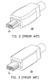
- FIG. 1 is a diagram illustrating that a plurality of USB pins are arranged in parallel within a conventional MINI AB connector.
- FIG. 2 and FIG. 3 respectively illustrate conventional MINI A and MINI B male joint connectors.
- FIG. 4 is a diagram of a connector according to an embodiment of the present invention.
- FIG. 5 illustrates a double-sided 11-pin male joint connector complying with USB specification which is suitable for the connector in FIG. 4.
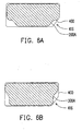
- FIG. 6A and FIG. 6B are diagrams illustrating the front plug-in of a male joint and a female joint.
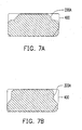
- FIG. 7A and FIG. 7B are diagrams illustrating the back plug-in of a male joint and a female joint.
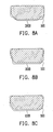
- FIGs. 8A ⁇ 8C are diagrams illustrating fool-proof when the male joint in the present invention is not suitable for the original MINI A, MINI B, and MINI AB female joints.
- FIG. 2 and FIG. 3 respectively illustrate conventional MINI A and MINI B male joint connectors.
- the 5 USB terminals (or pins) 210 in FIG. 2 are disposed on the MINI A connector 200 and can be used for signal transmission
- the 5 USB terminals (or pins) 310 in FIG. 3 are disposed on the MINI B connector 300, but the sizes and patterns of the interfaces are slightly different for preventing misplug or reverse plug, which may cause misjudgment or failure.
- the MINI A connector 200 and the MINI B connector 300 are only suitable for respective male joint or female joint since the MINI A connector 200 and the MINI B connector 300 are designed to be fool-proof.
- FIG. 4 is a diagram of a connector 400 according to an embodiment of the present invention
- FIG. 5 illustrates a double-sided 11-pin male joint connector 500 complying with USB specification which is suitable for the connector in FIG. 4.
- the difference of the connector 500 from the foregoing MINI A connector 200 and MINI B connector 300 is that the male joint connector 500 in FIG. 5 has 5 USB terminals (or pins) 510 located on the top surface of the interface and 6 USB terminals (or pins) 520 located on the bottom surface of the interface, and the total quantity of the terminals is 11.
- the 5 USB terminals 510 on the top surface of the interface can be served as the first set of signal terminals
- the 6 USB terminals 520 on the bottom surface of the interface can be served as the second set of signal terminals. Since the quantity of the first set of signal terminals is the same as the quantity of the original MINI A or MINI B USB terminals, the first set of signal terminals can be used as the USB terminals of the original peripheral device and it is not necessary to change the circuit design thereof.
- the newly added second set of signal terminals can be used along with the first set of signal terminals as the USB terminals of the newly developed peripheral device for function expansion.
- the present invention provides a connector 400 including a base 410, a plurality of first pins 420, and a plurality of second pins 430.
- the base 410 can be welded or assembled to an electronic apparatus (not shown), and the slot of the base 410 is used for accommodating a male joint having similar size to the slot, for example, the MINI A type connector 200 or the MINI B type connector 300 (first type joint), or the double-sided 11-pin male joint connector 500 (second type joint), so that the newly developed connector 400 can be suitable for different types of USB terminals.
- the base 410 includes a convex part 412 and a concave part 414 for accommodating the convex part 412, wherein a plurality of first pins 420 is disposed on the top surface of the convex.part 412 and is arranged in a row to form a first connecting surface. Besides, a plurality of second pins 430 is disposed on the bottom surface of the convex part 412 and is arranged in a row to form a second connecting surface. The first connecting surface and the second connecting surface are stacked on two opposite surfaces.
- the first pins 420 come into contact correspondingly with the terminals. 510 at one side in the male joint connector 500 and are turned on, and the second pins 430 come into contact correspondingly with the terminals 520 at the other side in the male joint connector 500 and are turned on. If the MINI A connector 200 or the MINI B connector 300 is plugged into the slot of the base 410, only the first pins 420 come into contact correspondingly with the terminals of the connector 200 or 300 to be turned on while the second pins 430 are left unused.
- the quantity of the first pins 420 complies with the pin quantity specified for MINI A or MINI B USB
- the total quantity of the first pins 420 and the second pins 430 complies with the pin quantity specified for double-sided 11-pin USB, that is, the total quantity of the first pins 420 is 5, and the total quantity of the second pins 430 is 6, and the total pin quantity of the second joint (double-sided 11-pin USB) is greater than the total pin quantity of the first joint (MINI A or MINI B USB).
- FIG. 6A and FIG. 6B are diagrams illustrating the correct plug-in of a male joint and a female joint
- FIG. 7A and FIG. 7B which are diagrams illustrating the reverse plug-in of a male joint and a female joint.
- the pattern of the connector 400 is designed to be fool-proof, that is, a concave edge portion 416 is designed for avoiding device failure or misjudgment.
- FIGs. 8A ⁇ 8C are diagrams illustrating fool-proof when the double-sided 11-pin male joint connector 500 in the present invention is not suitable for the original MINI A, MINI B, and MINI AB female joints.
- the pattern of the male joint 500 is purposely designed different from the original female joints, so that the newly developed male joint 500 cannot be plugged into the original host, accordingly the male joint 500 is prevented from being turned on mistakenly and the purpose of fool-proof is achieved.
- the connectors 400 and 500 keep the functions of the original 5-pin USB interface to be used by the original 5-pin MINI A and MINI B peripheral devices, and the USB interface of the newly added 6 pins is for function expansion so that the connector 400 can be used by the newly developed peripheral device, that is, the total quantity of the first pins and the newly added second pins can be used by the second kind of peripheral device having higher pin quantity.
- the type of the second joint can be determined based on the voltage variations of the first identification voltage and the second identification voltage, that is, the pre-classified second joint is determined based on the configuration of short circuit status, impedance status, and open circuit status between the two wires for connecting the host and the second joint.
- the newly added second pins 430 can be further disposed a ground pin corresponding to the ground terminal of the second joint to produce a common ground terminal.
- the second pins are also disposed with at least one audio pin to transmit audio signals.
- the foregoing identification pin, ground pin, and audio pin can be arranged and combined based on the circuit design and will not be described in detail herein.
- a connector structure compatible to typical MINI A and MINI B USB interfaces is adopted, and a set of independent functional pins are added to the original connector structure so that the first and the second joints having different pin quantities can both use the highly compatible connector structure.
- the connector of the present invention can meet function expansion requirement, and furthermore, the purpose of connector sharing in product design can be accomplished.
Landscapes
- Details Of Connecting Devices For Male And Female Coupling (AREA)
- Coupling Device And Connection With Printed Circuit (AREA)
- Multi-Conductor Connections (AREA)
Applications Claiming Priority (1)
| Application Number | Priority Date | Filing Date | Title |
|---|---|---|---|
| CNB2006100813958A CN100490258C (zh) | 2006-05-24 | 2006-05-24 | 用以共用不同接脚数的第一种接头与第二种接头的连接器 |
Publications (3)
| Publication Number | Publication Date |
|---|---|
| EP1860746A2 true EP1860746A2 (de) | 2007-11-28 |
| EP1860746A3 EP1860746A3 (de) | 2009-01-14 |
| EP1860746B1 EP1860746B1 (de) | 2011-11-30 |
Family
ID=38310232
Family Applications (1)
| Application Number | Title | Priority Date | Filing Date |
|---|---|---|---|
| EP07004894A Not-in-force EP1860746B1 (de) | 2006-05-24 | 2007-03-09 | Kompatibler Verbinder für Erst- und Zweitverbindungen mit unterschiedlicher Pinanzahl |
Country Status (3)
| Country | Link |
|---|---|
| EP (1) | EP1860746B1 (de) |
| CN (1) | CN100490258C (de) |
| AT (1) | ATE535969T1 (de) |
Cited By (4)
| Publication number | Priority date | Publication date | Assignee | Title |
|---|---|---|---|---|
| US7661993B2 (en) | 2008-06-16 | 2010-02-16 | Htc Corporation | Electronic device and receptacle connector thereof |
| US7670181B2 (en) | 2006-03-20 | 2010-03-02 | Htc Corporation | Connector for first and second joints having different pin quantities, electronic apparatus with connector and combination |
| TWI455420B (zh) * | 2012-01-10 | 2014-10-01 | Taiwin Electronics Co Ltd | 電連接器插座及其偵測方法 |
| US9219476B2 (en) | 2007-11-21 | 2015-12-22 | Nokia Corporation | Electronic device interface switching system |
Citations (1)
| Publication number | Priority date | Publication date | Assignee | Title |
|---|---|---|---|---|
| EP1274155A1 (de) | 2001-07-04 | 2003-01-08 | Japan Aviation Electronics Industry, Limited | Verbinder für Kupplung mit verschiedenen Verbindern die verschiedene Anpassungsformen ausweisen |
Family Cites Families (6)
| Publication number | Priority date | Publication date | Assignee | Title |
|---|---|---|---|---|
| US6299487B1 (en) * | 2000-04-03 | 2001-10-09 | Molex Incorporated | Connector with wear-resistant engagement means |
| JP2005071848A (ja) * | 2003-08-26 | 2005-03-17 | Kel Corp | プラグ型コネクタ、レセプタクル型コネクタ及び嵌合型コネクタ |
| TWM278139U (en) * | 2005-06-07 | 2005-10-11 | He And Technology Co Ltd | Small USB connector |
| JP4360364B2 (ja) * | 2005-08-26 | 2009-11-11 | パナソニック電工株式会社 | コネクタ |
| TWI304283B (en) * | 2006-03-20 | 2008-12-11 | Hith Tech Computer Corp | Connector |
| TWI302048B (en) * | 2006-03-20 | 2008-10-11 | Hith Tech Computer Corp | Compatible connector for first and second joints having different pin counts |
-
2006
- 2006-05-24 CN CNB2006100813958A patent/CN100490258C/zh not_active Expired - Fee Related
-
2007
- 2007-03-09 AT AT07004894T patent/ATE535969T1/de active
- 2007-03-09 EP EP07004894A patent/EP1860746B1/de not_active Not-in-force
Patent Citations (1)
| Publication number | Priority date | Publication date | Assignee | Title |
|---|---|---|---|---|
| EP1274155A1 (de) | 2001-07-04 | 2003-01-08 | Japan Aviation Electronics Industry, Limited | Verbinder für Kupplung mit verschiedenen Verbindern die verschiedene Anpassungsformen ausweisen |
Cited By (6)
| Publication number | Priority date | Publication date | Assignee | Title |
|---|---|---|---|---|
| US7670181B2 (en) | 2006-03-20 | 2010-03-02 | Htc Corporation | Connector for first and second joints having different pin quantities, electronic apparatus with connector and combination |
| US9219476B2 (en) | 2007-11-21 | 2015-12-22 | Nokia Corporation | Electronic device interface switching system |
| US7661993B2 (en) | 2008-06-16 | 2010-02-16 | Htc Corporation | Electronic device and receptacle connector thereof |
| EP2154756A1 (de) | 2008-06-16 | 2010-02-17 | High Tech Computer, Corp. | Elektronische Vorrichtung und Gehäusestecker dafür |
| EP2173013A1 (de) * | 2008-07-30 | 2010-04-07 | HTC Corporation | Verbinder für Erst- und Zweitverbindungen mit unterschiedlicher Pinanzahl, elektronisches Gerät mit Verbinder und Kombination |
| TWI455420B (zh) * | 2012-01-10 | 2014-10-01 | Taiwin Electronics Co Ltd | 電連接器插座及其偵測方法 |
Also Published As
| Publication number | Publication date |
|---|---|
| EP1860746A3 (de) | 2009-01-14 |
| EP1860746B1 (de) | 2011-11-30 |
| ATE535969T1 (de) | 2011-12-15 |
| CN100490258C (zh) | 2009-05-20 |
| CN101079528A (zh) | 2007-11-28 |
Similar Documents
| Publication | Publication Date | Title |
|---|---|---|
| US7427214B2 (en) | Compatible connector for first and second joints having different pin quantities | |
| US7670181B2 (en) | Connector for first and second joints having different pin quantities, electronic apparatus with connector and combination | |
| US6948983B1 (en) | Slim USB male connector with anti-disorientation design | |
| KR101193977B1 (ko) | 전기 커넥터 | |
| US7448917B2 (en) | Connector having pin groups with different pin lengths | |
| US20140329416A1 (en) | Connectors for electronic devices | |
| US8874819B2 (en) | USB connection cable | |
| US7988460B1 (en) | Electrical engagement structure of connection device | |
| US20130242497A1 (en) | Multi-serial port connection device and connection card thereof | |
| EP1860739B1 (de) | Verbinder mit Kontakten unterschiedlicher Länge | |
| WO2023109552A1 (zh) | 电子设备及信息卡识别方法 | |
| EP1860746B1 (de) | Kompatibler Verbinder für Erst- und Zweitverbindungen mit unterschiedlicher Pinanzahl | |
| CN201877657U (zh) | 插座连接器 | |
| WO2018045870A1 (en) | Usb type-c connector with a secondary port | |
| TWM579828U (zh) | Connector plug with guide post capable of guiding the tongue to accurately interface | |
| WO2023109643A1 (zh) | 电子设备及信息卡识别方法 | |
| WO2023109144A1 (zh) | 电子设备、卡连接器、卡座及卡座组件 | |
| US6896527B1 (en) | Slim USB male connector with system grounding | |
| US20130065448A1 (en) | Electronic connector | |
| CN106505346B (zh) | Usb连接器插座及usb连接器 | |
| US20070293267A1 (en) | Multi-function wireless transmission device | |
| US20140162501A1 (en) | Connector | |
| WO2023109682A1 (zh) | 存储卡 | |
| TWM631787U (zh) | 插座連接器 | |
| TWM629885U (zh) | 具有插接空間與導引結構的插座連接器 |
Legal Events
| Date | Code | Title | Description |
|---|---|---|---|
| PUAI | Public reference made under article 153(3) epc to a published international application that has entered the european phase |
Free format text: ORIGINAL CODE: 0009012 |
|
| AK | Designated contracting states |
Kind code of ref document: A2 Designated state(s): AT BE BG CH CY CZ DE DK EE ES FI FR GB GR HU IE IS IT LI LT LU LV MC MT NL PL PT RO SE SI SK TR |
|
| AX | Request for extension of the european patent |
Extension state: AL BA HR MK YU |
|
| 17P | Request for examination filed |
Effective date: 20080526 |
|
| PUAL | Search report despatched |
Free format text: ORIGINAL CODE: 0009013 |
|
| AK | Designated contracting states |
Kind code of ref document: A3 Designated state(s): AT BE BG CH CY CZ DE DK EE ES FI FR GB GR HU IE IS IT LI LT LU LV MC MT NL PL PT RO SE SI SK TR |
|
| AX | Request for extension of the european patent |
Extension state: AL BA HR MK RS |
|
| RIC1 | Information provided on ipc code assigned before grant |
Ipc: H01R 13/645 20060101ALI20081209BHEP Ipc: H01R 27/00 20060101AFI20070807BHEP |
|
| 17Q | First examination report despatched |
Effective date: 20090603 |
|
| AKX | Designation fees paid |
Designated state(s): AT BE BG CH CY CZ DE DK EE ES FI FR GB GR HU IE IS IT LI LT LU LV MC MT NL PL PT RO SE SI SK TR |
|
| RAP1 | Party data changed (applicant data changed or rights of an application transferred) |
Owner name: HTC CORPORATION |
|
| GRAP | Despatch of communication of intention to grant a patent |
Free format text: ORIGINAL CODE: EPIDOSNIGR1 |
|
| GRAS | Grant fee paid |
Free format text: ORIGINAL CODE: EPIDOSNIGR3 |
|
| GRAA | (expected) grant |
Free format text: ORIGINAL CODE: 0009210 |
|
| AK | Designated contracting states |
Kind code of ref document: B1 Designated state(s): AT BE BG CH CY CZ DE DK EE ES FI FR GB GR HU IE IS IT LI LT LU LV MC MT NL PL PT RO SE SI SK TR |
|
| REG | Reference to a national code |
Ref country code: GB Ref legal event code: FG4D Ref country code: CH Ref legal event code: EP |
|
| REG | Reference to a national code |
Ref country code: IE Ref legal event code: FG4D |
|
| REG | Reference to a national code |
Ref country code: DE Ref legal event code: R096 Ref document number: 602007018998 Country of ref document: DE Effective date: 20120209 |
|
| REG | Reference to a national code |
Ref country code: NL Ref legal event code: T3 |
|
| LTIE | Lt: invalidation of european patent or patent extension |
Effective date: 20111130 |
|
| PG25 | Lapsed in a contracting state [announced via postgrant information from national office to epo] |
Ref country code: IS Free format text: LAPSE BECAUSE OF FAILURE TO SUBMIT A TRANSLATION OF THE DESCRIPTION OR TO PAY THE FEE WITHIN THE PRESCRIBED TIME-LIMIT Effective date: 20120330 Ref country code: LT Free format text: LAPSE BECAUSE OF FAILURE TO SUBMIT A TRANSLATION OF THE DESCRIPTION OR TO PAY THE FEE WITHIN THE PRESCRIBED TIME-LIMIT Effective date: 20111130 |
|
| PG25 | Lapsed in a contracting state [announced via postgrant information from national office to epo] |
Ref country code: SE Free format text: LAPSE BECAUSE OF FAILURE TO SUBMIT A TRANSLATION OF THE DESCRIPTION OR TO PAY THE FEE WITHIN THE PRESCRIBED TIME-LIMIT Effective date: 20111130 Ref country code: SI Free format text: LAPSE BECAUSE OF FAILURE TO SUBMIT A TRANSLATION OF THE DESCRIPTION OR TO PAY THE FEE WITHIN THE PRESCRIBED TIME-LIMIT Effective date: 20111130 Ref country code: LV Free format text: LAPSE BECAUSE OF FAILURE TO SUBMIT A TRANSLATION OF THE DESCRIPTION OR TO PAY THE FEE WITHIN THE PRESCRIBED TIME-LIMIT Effective date: 20111130 Ref country code: GR Free format text: LAPSE BECAUSE OF FAILURE TO SUBMIT A TRANSLATION OF THE DESCRIPTION OR TO PAY THE FEE WITHIN THE PRESCRIBED TIME-LIMIT Effective date: 20120301 Ref country code: PT Free format text: LAPSE BECAUSE OF FAILURE TO SUBMIT A TRANSLATION OF THE DESCRIPTION OR TO PAY THE FEE WITHIN THE PRESCRIBED TIME-LIMIT Effective date: 20120330 |
|
| PG25 | Lapsed in a contracting state [announced via postgrant information from national office to epo] |
Ref country code: CY Free format text: LAPSE BECAUSE OF FAILURE TO SUBMIT A TRANSLATION OF THE DESCRIPTION OR TO PAY THE FEE WITHIN THE PRESCRIBED TIME-LIMIT Effective date: 20111130 |
|
| PG25 | Lapsed in a contracting state [announced via postgrant information from national office to epo] |
Ref country code: SK Free format text: LAPSE BECAUSE OF FAILURE TO SUBMIT A TRANSLATION OF THE DESCRIPTION OR TO PAY THE FEE WITHIN THE PRESCRIBED TIME-LIMIT Effective date: 20111130 Ref country code: EE Free format text: LAPSE BECAUSE OF FAILURE TO SUBMIT A TRANSLATION OF THE DESCRIPTION OR TO PAY THE FEE WITHIN THE PRESCRIBED TIME-LIMIT Effective date: 20111130 Ref country code: CZ Free format text: LAPSE BECAUSE OF FAILURE TO SUBMIT A TRANSLATION OF THE DESCRIPTION OR TO PAY THE FEE WITHIN THE PRESCRIBED TIME-LIMIT Effective date: 20111130 Ref country code: DK Free format text: LAPSE BECAUSE OF FAILURE TO SUBMIT A TRANSLATION OF THE DESCRIPTION OR TO PAY THE FEE WITHIN THE PRESCRIBED TIME-LIMIT Effective date: 20111130 Ref country code: BG Free format text: LAPSE BECAUSE OF FAILURE TO SUBMIT A TRANSLATION OF THE DESCRIPTION OR TO PAY THE FEE WITHIN THE PRESCRIBED TIME-LIMIT Effective date: 20120229 |
|
| PG25 | Lapsed in a contracting state [announced via postgrant information from national office to epo] |
Ref country code: RO Free format text: LAPSE BECAUSE OF FAILURE TO SUBMIT A TRANSLATION OF THE DESCRIPTION OR TO PAY THE FEE WITHIN THE PRESCRIBED TIME-LIMIT Effective date: 20111130 Ref country code: PL Free format text: LAPSE BECAUSE OF FAILURE TO SUBMIT A TRANSLATION OF THE DESCRIPTION OR TO PAY THE FEE WITHIN THE PRESCRIBED TIME-LIMIT Effective date: 20111130 Ref country code: IT Free format text: LAPSE BECAUSE OF FAILURE TO SUBMIT A TRANSLATION OF THE DESCRIPTION OR TO PAY THE FEE WITHIN THE PRESCRIBED TIME-LIMIT Effective date: 20111130 |
|
| REG | Reference to a national code |
Ref country code: AT Ref legal event code: MK05 Ref document number: 535969 Country of ref document: AT Kind code of ref document: T Effective date: 20111130 |
|
| PLBE | No opposition filed within time limit |
Free format text: ORIGINAL CODE: 0009261 |
|
| STAA | Information on the status of an ep patent application or granted ep patent |
Free format text: STATUS: NO OPPOSITION FILED WITHIN TIME LIMIT |
|
| PG25 | Lapsed in a contracting state [announced via postgrant information from national office to epo] |
Ref country code: MC Free format text: LAPSE BECAUSE OF NON-PAYMENT OF DUE FEES Effective date: 20120331 |
|
| REG | Reference to a national code |
Ref country code: CH Ref legal event code: PL |
|
| 26N | No opposition filed |
Effective date: 20120831 |
|
| REG | Reference to a national code |
Ref country code: DE Ref legal event code: R097 Ref document number: 602007018998 Country of ref document: DE Effective date: 20120831 |
|
| REG | Reference to a national code |
Ref country code: IE Ref legal event code: MM4A |
|
| PG25 | Lapsed in a contracting state [announced via postgrant information from national office to epo] |
Ref country code: LI Free format text: LAPSE BECAUSE OF NON-PAYMENT OF DUE FEES Effective date: 20120331 Ref country code: IE Free format text: LAPSE BECAUSE OF NON-PAYMENT OF DUE FEES Effective date: 20120309 Ref country code: AT Free format text: LAPSE BECAUSE OF FAILURE TO SUBMIT A TRANSLATION OF THE DESCRIPTION OR TO PAY THE FEE WITHIN THE PRESCRIBED TIME-LIMIT Effective date: 20111130 Ref country code: CH Free format text: LAPSE BECAUSE OF NON-PAYMENT OF DUE FEES Effective date: 20120331 |
|
| PG25 | Lapsed in a contracting state [announced via postgrant information from national office to epo] |
Ref country code: ES Free format text: LAPSE BECAUSE OF FAILURE TO SUBMIT A TRANSLATION OF THE DESCRIPTION OR TO PAY THE FEE WITHIN THE PRESCRIBED TIME-LIMIT Effective date: 20120311 |
|
| PG25 | Lapsed in a contracting state [announced via postgrant information from national office to epo] |
Ref country code: FI Free format text: LAPSE BECAUSE OF FAILURE TO SUBMIT A TRANSLATION OF THE DESCRIPTION OR TO PAY THE FEE WITHIN THE PRESCRIBED TIME-LIMIT Effective date: 20111130 |
|
| PG25 | Lapsed in a contracting state [announced via postgrant information from national office to epo] |
Ref country code: MT Free format text: LAPSE BECAUSE OF FAILURE TO SUBMIT A TRANSLATION OF THE DESCRIPTION OR TO PAY THE FEE WITHIN THE PRESCRIBED TIME-LIMIT Effective date: 20111130 |
|
| PG25 | Lapsed in a contracting state [announced via postgrant information from national office to epo] |
Ref country code: TR Free format text: LAPSE BECAUSE OF FAILURE TO SUBMIT A TRANSLATION OF THE DESCRIPTION OR TO PAY THE FEE WITHIN THE PRESCRIBED TIME-LIMIT Effective date: 20111130 |
|
| PG25 | Lapsed in a contracting state [announced via postgrant information from national office to epo] |
Ref country code: LU Free format text: LAPSE BECAUSE OF NON-PAYMENT OF DUE FEES Effective date: 20120309 |
|
| PG25 | Lapsed in a contracting state [announced via postgrant information from national office to epo] |
Ref country code: HU Free format text: LAPSE BECAUSE OF FAILURE TO SUBMIT A TRANSLATION OF THE DESCRIPTION OR TO PAY THE FEE WITHIN THE PRESCRIBED TIME-LIMIT Effective date: 20070309 |
|
| REG | Reference to a national code |
Ref country code: FR Ref legal event code: PLFP Year of fee payment: 9 |
|
| REG | Reference to a national code |
Ref country code: FR Ref legal event code: PLFP Year of fee payment: 10 |
|
| REG | Reference to a national code |
Ref country code: FR Ref legal event code: PLFP Year of fee payment: 11 |
|
| REG | Reference to a national code |
Ref country code: FR Ref legal event code: PLFP Year of fee payment: 12 |
|
| PGFP | Annual fee paid to national office [announced via postgrant information from national office to epo] |
Ref country code: DE Payment date: 20190226 Year of fee payment: 13 Ref country code: GB Payment date: 20190306 Year of fee payment: 13 |
|
| PGFP | Annual fee paid to national office [announced via postgrant information from national office to epo] |
Ref country code: DE Payment date: 20190226 Year of fee payment: 13 Ref country code: FR Payment date: 20190213 Year of fee payment: 13 Ref country code: NL Payment date: 20190313 Year of fee payment: 13 Ref country code: BE Payment date: 20190116 Year of fee payment: 13 |
|
| REG | Reference to a national code |
Ref country code: DE Ref legal event code: R119 Ref document number: 602007018998 Country of ref document: DE |
|
| REG | Reference to a national code |
Ref country code: NL Ref legal event code: MM Effective date: 20200401 |
|
| REG | Reference to a national code |
Ref country code: BE Ref legal event code: MM Effective date: 20200331 |
|
| PG25 | Lapsed in a contracting state [announced via postgrant information from national office to epo] |
Ref country code: NL Free format text: LAPSE BECAUSE OF NON-PAYMENT OF DUE FEES Effective date: 20200401 |
|
| PG25 | Lapsed in a contracting state [announced via postgrant information from national office to epo] |
Ref country code: DE Free format text: LAPSE BECAUSE OF NON-PAYMENT OF DUE FEES Effective date: 20201001 Ref country code: FR Free format text: LAPSE BECAUSE OF NON-PAYMENT OF DUE FEES Effective date: 20200331 |
|
| PG25 | Lapsed in a contracting state [announced via postgrant information from national office to epo] |
Ref country code: BE Free format text: LAPSE BECAUSE OF NON-PAYMENT OF DUE FEES Effective date: 20200331 |
|
| GBPC | Gb: european patent ceased through non-payment of renewal fee |
Effective date: 20200309 |
|
| PG25 | Lapsed in a contracting state [announced via postgrant information from national office to epo] |
Ref country code: GB Free format text: LAPSE BECAUSE OF NON-PAYMENT OF DUE FEES Effective date: 20200309 |