EP1858080A2 - No-lead ic packages having integrated heat spreader for electromagnetic interference (emi) shielding and thermal enhancement - Google Patents
No-lead ic packages having integrated heat spreader for electromagnetic interference (emi) shielding and thermal enhancement Download PDFInfo
- Publication number
- EP1858080A2 EP1858080A2 EP20060026677 EP06026677A EP1858080A2 EP 1858080 A2 EP1858080 A2 EP 1858080A2 EP 20060026677 EP20060026677 EP 20060026677 EP 06026677 A EP06026677 A EP 06026677A EP 1858080 A2 EP1858080 A2 EP 1858080A2
- Authority
- EP
- European Patent Office
- Prior art keywords
- die
- leadframe
- package
- cap
- leads
- Prior art date
- Legal status (The legal status is an assumption and is not a legal conclusion. Google has not performed a legal analysis and makes no representation as to the accuracy of the status listed.)
- Withdrawn
Links
Images









Classifications
-
- H—ELECTRICITY
- H10—SEMICONDUCTOR DEVICES; ELECTRIC SOLID-STATE DEVICES NOT OTHERWISE PROVIDED FOR
- H10W—GENERIC PACKAGES, INTERCONNECTIONS, CONNECTORS OR OTHER CONSTRUCTIONAL DETAILS OF DEVICES COVERED BY CLASS H10
- H10W42/00—Arrangements for protection of devices
- H10W42/20—Arrangements for protection of devices protecting against electromagnetic or particle radiation, e.g. light, X-rays, gamma-rays or electrons
-
- H—ELECTRICITY
- H10—SEMICONDUCTOR DEVICES; ELECTRIC SOLID-STATE DEVICES NOT OTHERWISE PROVIDED FOR
- H10W—GENERIC PACKAGES, INTERCONNECTIONS, CONNECTORS OR OTHER CONSTRUCTIONAL DETAILS OF DEVICES COVERED BY CLASS H10
- H10W40/00—Arrangements for thermal protection or thermal control
- H10W40/70—Fillings or auxiliary members in containers or in encapsulations for thermal protection or control
- H10W40/77—Auxiliary members characterised by their shape
- H10W40/778—Auxiliary members characterised by their shape in encapsulations
-
- H—ELECTRICITY
- H10—SEMICONDUCTOR DEVICES; ELECTRIC SOLID-STATE DEVICES NOT OTHERWISE PROVIDED FOR
- H10W—GENERIC PACKAGES, INTERCONNECTIONS, CONNECTORS OR OTHER CONSTRUCTIONAL DETAILS OF DEVICES COVERED BY CLASS H10
- H10W70/00—Package substrates; Interposers; Redistribution layers [RDL]
- H10W70/40—Leadframes
- H10W70/411—Chip-supporting parts, e.g. die pads
-
- H—ELECTRICITY
- H10—SEMICONDUCTOR DEVICES; ELECTRIC SOLID-STATE DEVICES NOT OTHERWISE PROVIDED FOR
- H10W—GENERIC PACKAGES, INTERCONNECTIONS, CONNECTORS OR OTHER CONSTRUCTIONAL DETAILS OF DEVICES COVERED BY CLASS H10
- H10W74/00—Encapsulations, e.g. protective coatings
- H10W74/01—Manufacture or treatment
- H10W74/014—Manufacture or treatment using batch processing
-
- H—ELECTRICITY
- H10—SEMICONDUCTOR DEVICES; ELECTRIC SOLID-STATE DEVICES NOT OTHERWISE PROVIDED FOR
- H10W—GENERIC PACKAGES, INTERCONNECTIONS, CONNECTORS OR OTHER CONSTRUCTIONAL DETAILS OF DEVICES COVERED BY CLASS H10
- H10W74/00—Encapsulations, e.g. protective coatings
- H10W74/10—Encapsulations, e.g. protective coatings characterised by their shape or disposition
- H10W74/111—Encapsulations, e.g. protective coatings characterised by their shape or disposition the semiconductor body being completely enclosed
-
- H—ELECTRICITY
- H10—SEMICONDUCTOR DEVICES; ELECTRIC SOLID-STATE DEVICES NOT OTHERWISE PROVIDED FOR
- H10W—GENERIC PACKAGES, INTERCONNECTIONS, CONNECTORS OR OTHER CONSTRUCTIONAL DETAILS OF DEVICES COVERED BY CLASS H10
- H10W74/00—Encapsulations, e.g. protective coatings
- H10W74/10—Encapsulations, e.g. protective coatings characterised by their shape or disposition
- H10W74/111—Encapsulations, e.g. protective coatings characterised by their shape or disposition the semiconductor body being completely enclosed
- H10W74/114—Encapsulations, e.g. protective coatings characterised by their shape or disposition the semiconductor body being completely enclosed by a substrate and the encapsulations
- H10W74/117—Encapsulations, e.g. protective coatings characterised by their shape or disposition the semiconductor body being completely enclosed by a substrate and the encapsulations the substrate having spherical bumps for external connection
-
- H—ELECTRICITY
- H10—SEMICONDUCTOR DEVICES; ELECTRIC SOLID-STATE DEVICES NOT OTHERWISE PROVIDED FOR
- H10W—GENERIC PACKAGES, INTERCONNECTIONS, CONNECTORS OR OTHER CONSTRUCTIONAL DETAILS OF DEVICES COVERED BY CLASS H10
- H10W72/00—Interconnections or connectors in packages
- H10W72/01—Manufacture or treatment
- H10W72/0198—Manufacture or treatment batch processes
-
- H—ELECTRICITY
- H10—SEMICONDUCTOR DEVICES; ELECTRIC SOLID-STATE DEVICES NOT OTHERWISE PROVIDED FOR
- H10W—GENERIC PACKAGES, INTERCONNECTIONS, CONNECTORS OR OTHER CONSTRUCTIONAL DETAILS OF DEVICES COVERED BY CLASS H10
- H10W72/00—Interconnections or connectors in packages
- H10W72/071—Connecting or disconnecting
- H10W72/075—Connecting or disconnecting of bond wires
- H10W72/07551—Connecting or disconnecting of bond wires characterised by changes in properties of the bond wires during the connecting
- H10W72/07554—Connecting or disconnecting of bond wires characterised by changes in properties of the bond wires during the connecting changes in dispositions
-
- H—ELECTRICITY
- H10—SEMICONDUCTOR DEVICES; ELECTRIC SOLID-STATE DEVICES NOT OTHERWISE PROVIDED FOR
- H10W—GENERIC PACKAGES, INTERCONNECTIONS, CONNECTORS OR OTHER CONSTRUCTIONAL DETAILS OF DEVICES COVERED BY CLASS H10
- H10W72/00—Interconnections or connectors in packages
- H10W72/30—Die-attach connectors
- H10W72/351—Materials of die-attach connectors
- H10W72/353—Materials of die-attach connectors not comprising solid metals or solid metalloids, e.g. ceramics
- H10W72/354—Materials of die-attach connectors not comprising solid metals or solid metalloids, e.g. ceramics comprising polymers
-
- H—ELECTRICITY
- H10—SEMICONDUCTOR DEVICES; ELECTRIC SOLID-STATE DEVICES NOT OTHERWISE PROVIDED FOR
- H10W—GENERIC PACKAGES, INTERCONNECTIONS, CONNECTORS OR OTHER CONSTRUCTIONAL DETAILS OF DEVICES COVERED BY CLASS H10
- H10W72/00—Interconnections or connectors in packages
- H10W72/50—Bond wires
- H10W72/541—Dispositions of bond wires
- H10W72/5449—Dispositions of bond wires not being orthogonal to a side surface of the chip, e.g. fan-out arrangements
-
- H—ELECTRICITY
- H10—SEMICONDUCTOR DEVICES; ELECTRIC SOLID-STATE DEVICES NOT OTHERWISE PROVIDED FOR
- H10W—GENERIC PACKAGES, INTERCONNECTIONS, CONNECTORS OR OTHER CONSTRUCTIONAL DETAILS OF DEVICES COVERED BY CLASS H10
- H10W72/00—Interconnections or connectors in packages
- H10W72/50—Bond wires
- H10W72/541—Dispositions of bond wires
- H10W72/547—Dispositions of multiple bond wires
-
- H—ELECTRICITY
- H10—SEMICONDUCTOR DEVICES; ELECTRIC SOLID-STATE DEVICES NOT OTHERWISE PROVIDED FOR
- H10W—GENERIC PACKAGES, INTERCONNECTIONS, CONNECTORS OR OTHER CONSTRUCTIONAL DETAILS OF DEVICES COVERED BY CLASS H10
- H10W72/00—Interconnections or connectors in packages
- H10W72/50—Bond wires
- H10W72/541—Dispositions of bond wires
- H10W72/547—Dispositions of multiple bond wires
- H10W72/5473—Dispositions of multiple bond wires multiple bond wires connected to a common bond pad
-
- H—ELECTRICITY
- H10—SEMICONDUCTOR DEVICES; ELECTRIC SOLID-STATE DEVICES NOT OTHERWISE PROVIDED FOR
- H10W—GENERIC PACKAGES, INTERCONNECTIONS, CONNECTORS OR OTHER CONSTRUCTIONAL DETAILS OF DEVICES COVERED BY CLASS H10
- H10W72/00—Interconnections or connectors in packages
- H10W72/50—Bond wires
- H10W72/551—Materials of bond wires
- H10W72/552—Materials of bond wires comprising metals or metalloids, e.g. silver
-
- H—ELECTRICITY
- H10—SEMICONDUCTOR DEVICES; ELECTRIC SOLID-STATE DEVICES NOT OTHERWISE PROVIDED FOR
- H10W—GENERIC PACKAGES, INTERCONNECTIONS, CONNECTORS OR OTHER CONSTRUCTIONAL DETAILS OF DEVICES COVERED BY CLASS H10
- H10W72/00—Interconnections or connectors in packages
- H10W72/851—Dispositions of multiple connectors or interconnections
- H10W72/874—On different surfaces
- H10W72/884—Die-attach connectors and bond wires
-
- H—ELECTRICITY
- H10—SEMICONDUCTOR DEVICES; ELECTRIC SOLID-STATE DEVICES NOT OTHERWISE PROVIDED FOR
- H10W—GENERIC PACKAGES, INTERCONNECTIONS, CONNECTORS OR OTHER CONSTRUCTIONAL DETAILS OF DEVICES COVERED BY CLASS H10
- H10W74/00—Encapsulations, e.g. protective coatings
-
- H—ELECTRICITY
- H10—SEMICONDUCTOR DEVICES; ELECTRIC SOLID-STATE DEVICES NOT OTHERWISE PROVIDED FOR
- H10W—GENERIC PACKAGES, INTERCONNECTIONS, CONNECTORS OR OTHER CONSTRUCTIONAL DETAILS OF DEVICES COVERED BY CLASS H10
- H10W76/00—Containers; Fillings or auxiliary members therefor; Seals
- H10W76/10—Containers or parts thereof
- H10W76/17—Containers or parts thereof characterised by their materials
-
- H—ELECTRICITY
- H10—SEMICONDUCTOR DEVICES; ELECTRIC SOLID-STATE DEVICES NOT OTHERWISE PROVIDED FOR
- H10W—GENERIC PACKAGES, INTERCONNECTIONS, CONNECTORS OR OTHER CONSTRUCTIONAL DETAILS OF DEVICES COVERED BY CLASS H10
- H10W90/00—Package configurations
- H10W90/701—Package configurations characterised by the relative positions of pads or connectors relative to package parts
-
- H—ELECTRICITY
- H10—SEMICONDUCTOR DEVICES; ELECTRIC SOLID-STATE DEVICES NOT OTHERWISE PROVIDED FOR
- H10W—GENERIC PACKAGES, INTERCONNECTIONS, CONNECTORS OR OTHER CONSTRUCTIONAL DETAILS OF DEVICES COVERED BY CLASS H10
- H10W90/00—Package configurations
- H10W90/701—Package configurations characterised by the relative positions of pads or connectors relative to package parts
- H10W90/731—Package configurations characterised by the relative positions of pads or connectors relative to package parts of die-attach connectors
- H10W90/734—Package configurations characterised by the relative positions of pads or connectors relative to package parts of die-attach connectors between a chip and a stacked insulating package substrate, interposer or RDL
-
- H—ELECTRICITY
- H10—SEMICONDUCTOR DEVICES; ELECTRIC SOLID-STATE DEVICES NOT OTHERWISE PROVIDED FOR
- H10W—GENERIC PACKAGES, INTERCONNECTIONS, CONNECTORS OR OTHER CONSTRUCTIONAL DETAILS OF DEVICES COVERED BY CLASS H10
- H10W90/00—Package configurations
- H10W90/701—Package configurations characterised by the relative positions of pads or connectors relative to package parts
- H10W90/731—Package configurations characterised by the relative positions of pads or connectors relative to package parts of die-attach connectors
- H10W90/736—Package configurations characterised by the relative positions of pads or connectors relative to package parts of die-attach connectors between a chip and a stacked lead frame, conducting package substrate or heat sink
-
- H—ELECTRICITY
- H10—SEMICONDUCTOR DEVICES; ELECTRIC SOLID-STATE DEVICES NOT OTHERWISE PROVIDED FOR
- H10W—GENERIC PACKAGES, INTERCONNECTIONS, CONNECTORS OR OTHER CONSTRUCTIONAL DETAILS OF DEVICES COVERED BY CLASS H10
- H10W90/00—Package configurations
- H10W90/701—Package configurations characterised by the relative positions of pads or connectors relative to package parts
- H10W90/751—Package configurations characterised by the relative positions of pads or connectors relative to package parts of bond wires
- H10W90/754—Package configurations characterised by the relative positions of pads or connectors relative to package parts of bond wires between a chip and a stacked insulating package substrate, interposer or RDL
-
- H—ELECTRICITY
- H10—SEMICONDUCTOR DEVICES; ELECTRIC SOLID-STATE DEVICES NOT OTHERWISE PROVIDED FOR
- H10W—GENERIC PACKAGES, INTERCONNECTIONS, CONNECTORS OR OTHER CONSTRUCTIONAL DETAILS OF DEVICES COVERED BY CLASS H10
- H10W90/00—Package configurations
- H10W90/701—Package configurations characterised by the relative positions of pads or connectors relative to package parts
- H10W90/751—Package configurations characterised by the relative positions of pads or connectors relative to package parts of bond wires
- H10W90/756—Package configurations characterised by the relative positions of pads or connectors relative to package parts of bond wires between a chip and a stacked lead frame, conducting package substrate or heat sink
-
- H—ELECTRICITY
- H10—SEMICONDUCTOR DEVICES; ELECTRIC SOLID-STATE DEVICES NOT OTHERWISE PROVIDED FOR
- H10W—GENERIC PACKAGES, INTERCONNECTIONS, CONNECTORS OR OTHER CONSTRUCTIONAL DETAILS OF DEVICES COVERED BY CLASS H10
- H10W99/00—Subject matter not provided for in other groups of this subclass
Definitions
- the invention relates generally to the field of integrated circuit (IC) device packaging technology, and more particularly to thermal enhancement and electromagnetic interference (EMI) shielding in no-lead packages for IC devices.
- IC integrated circuit
- EMI electromagnetic interference
- Integrated circuit (IC) semiconductor chips or dies are typically mounted in or on a package that is attached to a printed circuit board (PCB) or printed wire board (PWB).
- PCB printed circuit board
- PWB printed wire board
- the structural frame, typically made of metal or some other conductor, to which semiconductor dies are attached during the package assembly process is known as a leadframe.
- a leadframe is widely used in IC packages as a carrier for the IC die and as an interconnection mechanism between the die and the electrical circuits of the PCB/PWB.
- a leadframe can have positions allocated for housing multiple IC dies. After dies are attached to the leadframe, metal wires are used to connect the IC die bond pads to the leadframe bond pads, which are sometimes known as bond fingers.
- the positions on the leadframe where dies are located are encapsulated in a molding compound, such as thermoset epoxy.
- a molding compound such as thermoset epoxy.
- encapsulated chips are mechanically broken loose from the leadframe rails. If parts of the leadframe protrude from the package, the package is called a leaded package. In contrast, if the package leads do not substantially protrude from the leadframe footprint, then the package is called a no-lead leadframe package or simply, a no-lead package or leadless package. In a no-lead package, straight or bended leads are bent downwards and/or inwards to be mounted on a PCB/PWB substrate.
- a variation of a no-lead leadframe package has an exposed die attach pad (DAP).
- the exposed DAP has a solderable outer surface opposite to the die attach surface which can be solder attached to a PCB/PWB.
- Another alternative no-lead package is known as a Thin Array Plastic Package (TAPP), which has multiple rows of peripheral leads for wire bonding.
- TAPP Thin Array Plastic Package
- the present invention is directed to methods and apparatus for improved thermal performance and EMI shielding in IC packages.
- an IC device package includes a cap having opposing first and second surfaces. A first portion of the second surface of the cap has a cavity formed therein. A planar second portion of the second surface of the cap is coupled to a DAP. The DAP has a central portion, and a plurality of tie bars coupled to the central portion of the DAP. An IC die is mounted to the central portion of the DAP. The cap and the DAP form an encasing structure that substantially encloses the IC die(s).
- an IC device package is assembled.
- a leadframe tailored for a no-lead package is formed.
- An IC die is attached to a central portion of the die attach pad of the leadframe. Wire bonds are coupled between the IC die and the leadframe.
- a cap is attached to the leadframe. A second surface of the cap includes a cavity.
- the cap and the leadframe form an encasing structure that substantially encloses the IC die.
- a molding material is applied to encapsulate the IC die.
- a perimeter support ring portion of the leadframe is trimmed. Portions of the leads are bent to aid coupling of the leads to a circuit board.
- the encasing structure spreads heat from the IC die(s) during operation. Furthermore, the encasing structure shields EMI emanating from the IC die(s) and EMI radiating toward the IC die(s) from outside the package.
- an integrated circuit (IC) device package comprising:
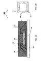
- FIGs. 1A, 1B, 2A, 2B, 3A, and 3B show cross-sectional and bottom views of various types of IC packages with exposed DAP for improved thermal performance.
- FIG. 4 illustrates an example ball grid array (BGA) IC package.
- BGA ball grid array
- FIGs. 5A-5F show examples of caps according to embodiments of the invention.
- FIGs. 6A-6C show plan views of examples of leadframes according to embodiments of the invention.
- FIGs. 7A-7F show cross sectional views of examples of IC packages with integrated heat spreader caps according to embodiments of the invention.
- FIG. 8 shows a flowchart illustrating example steps for assembling leadframe IC packages, according to embodiments of the invention.
- FIGs. 9A-9D show plan views of examples of leadframe IC packages undergoing assembly, according to embodiments of the invention.
- FIGs. 9E-9G show side views of examples of leadframe IC packages undergoing assembly, according to embodiments of the invention.
- FIG. 10 shows a flowchart illustrating example steps for assembling leadframe IC packages in an alternative process different from FIG. 8.
- FIGs. 11A-11C illustrate an example method for attaching a cap to a leadframe after encapsulation.
- the present invention is directed to methods and apparatus for improving thermal performance and electromagnetic interference (EMI) shielding in integrated circuit (IC) packages.
- An IC die is mounted to a DAP.
- the IC die may be mounted in a die-up configuration, where the die is attached to a surface of the DAP that is facing away from a board (such as a PCB).
- the IC die may also be mounted in a die-down configuration, where the die is attached to a surface of the DAP that is facing towards the board.
- Wire bonds may be used to electrically connect bond pads patterned on the die to lead fingers surrounding the DAP. Note that the base region of a lead to which a wire bond is connected is referred to as a "lead finger".
- CSP Chip Scale Package
- LPCC Leadless Plastic Chip Carrier
- MLP Micro Leadframe Package
- TAPP packages which have multiple rows of peripheral leads for wire bonding.
- TAPP packages are assembled with a unique process that allows for multi-row peripheral outputs as well as ground or power interposer rings.
- the packages are extremely thin with a nominal thickness in the range of 0.7mm, and Input/Output (I/O) densities comparable with fine pitch Ball Grid Array (fpBGA) packages.
- I/O Input/Output
- fpBGA Ball Grid Array
- a modified version of a TAPP-type package can be assembled from an appropriately designed leadframe having multiple peripheral lead rows, where each of the rows have a corresponding perimeter support ring.
- One or more interposer ground/power rings may also be coupled to the DAP.
- a metal cap is coupled (e.g. electrically, structurally, and/or thermally connected) to the DAP to form an encasing structure.
- the coupling may be effected with or without the use of a thermally and/or electrically conductive adhesive, such as solder or epoxy with metal particles or flakes.
- the cap is coupled to the tie bars attaching one or more leads to the DAP.
- the tie bars may be widened or fused to leads.
- the cap is coupled to the leads.
- the cap is coupled to the DAP.
- the cap may be coupled with any combination of DAP, leads, and tie bars. Tabs on the cap mate with matching receptacles on one or more fused leads and/or tie bars to improve coupling and overall structural strength.
- the encasing structure formed by a cap and a DAP approximates an equipotential surface, known as a "Faraday Cage", surrounding the die and the interconnections.
- the encasing structure material is typically a very good conductor of heat, and is relatively rigid (e.g., copper or copper alloy C151).
- the encasing structure may provide improved EMI shielding, improved heat transfer from the IC die, enhanced rigidity of the package, and improved environmental (e.g., mechanical shock, vibration, impact, stress, temperature, moisture, corrosion, etc.) protection.
- the die and the wire bond are encapsulated in a molding material, which provides environmental protection.
- the molding material may also completely cover the cap. In other embodiments, the cap is partially covered, or is not covered by the molding material.
- Common plastic molding compound encapsulated leadframe packages exhibit poor thermal performance, because there is no continuous heat dissipation path between the DAP and the leads. Heat generated on the active surface of the IC die is dissipated primarily through the top and bottom surfaces of the package.
- the leadframe conducts some heat into a PCB/PWB to which the package is attached.
- the molding material that encapsulates the IC die transfers some heat to the environment through various convection paths and radiation paths.
- Typical molding materials have a low thermal conductivity value, such as around or between 0.2 ⁇ 0.9 W/m ⁇ K. Therefore, molding materials in conventional leadframe packages impose the primary bottleneck for heat dissipation from the die to the external surfaces and terminal leads of the package.
- Thermal performance of leaded and no-lead leadframe packages can be improved by exposing the DAP at the bottom surface of molding material.
- FIGs. 1A and 1B are respectively side and bottom views of a leaded PQFP package 100 with an exposed DAP.
- Package 100 comprises IC die 150, DAP 140, wirebonds 130, molding material 120, adhesive 170, and package leads 180.
- DAP 140 and package leads 180 may be part of a leadframe.
- IC die 150 is mounted on DAP 140 with adhesive 170.
- Molding material 120 encapsulates IC die 150 and wirebonds 130.
- Wirebonds 130 connect the bond pads on IC die 150 to package leads 180. Additional wirebonds 130 may be formed between the IC die and DAP 140, and DAP 140 and leads 180, as shown in FIG. 1A. and DAP 140 has at least a portion of its outer surface exposed.
- PCB/PWB 160 acts as a heat spreader for the package, as the heat generated on the active surface of die 150 is dissipated into PCB/PWB 160 with very low conductive thermal resistances.
- This type of package is referred to as an "Exposed Pad Thin Quad Flat Pack" or eTQFP package.
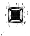
- FIGs. 2A and 2B are respectively side and bottom views of a no-lead leadframe package 200 with exposed DAP 140.
- Package 200 comprises IC die 150, DAP 140, wirebonds 130, molding material 120, adhesive 170, and package leads 280.
- DAP 140 and package leads 280 may be part of a leadframe.
- IC die 150 is mounted on DAP 140 with adhesive 170.
- Molding material 120 encapsulates IC die 150 and wire bonds 130. At least a portion of the outer surface of DAP 140 is coated with a thermally conducting solder or adhesive, which bonds package 200 to a PCB/PWB 160.
- MLP Micro Leadframe Package
- QFN Quad Flat No-Lead
- package leads 280 do not protrude substantially from the package outline.
- Package leads 280 surround DAP 140. In a no-lead package such as package 200, typically, there is only one row of peripheral leads. Wire bonds 130 connect leads 280 to bond pads on IC die 150. DAP 140 may be connected to ground potential or a certain power potential.
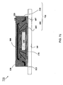
- FIGs. 3A and 3B are respectively side and bottom views of a no-lead TAPP-type package 300 with exposed DAP 140.
- Package 300 comprises IC die 150, DAP 140, wirebonds 130, molding material 120, adhesive 170, interposer ring 390, and package leads 385.
- the outer surface of DAP 140 is coated with a thermally conducting solder or adhesive, which bonds package 300 to a PCB/PWB 160.
- Leads 385 surround DAP 140 in more than one row forming an array of output leads.
- Wire bonds 130 connect leads 385 to corresponding bond pads on IC die 150. Having multiple rows of package leads increases I/O density of the packaged circuit. Additionally, one or more interposer rings 390 may be included in the package.
- Interposer ring 390 is typically coupled to ground potential. Note that interposer ring 390 does not necessarily have to be connected to ground. It can be connected to a certain power potential as well.
- TAPP packages have a unique assembly process. However, as mentioned earlier, TAPP-type packages can have a leadframe-based assembly process, if the leadframe design is modified to include interposer rings and multiple peripheral lead rows.
- EMI electromagnetic interference
- a change in the electrical current carried by a conductor results in the radiation of electromagnetic waves. Such waves propagate through space at the speed of light, and when not wanted, are called EMI.
- a relatively slow change in the electrical current causes a small amount of electromagnetic radiation with a long wavelength and a low frequency.
- a relatively rapid change in the electrical current causes a large amount of radiation with a short wavelength and a high frequency.
- the unwanted high frequency electromagnetic radiation is sometimes called radio-frequency interference (RFI), but in the interest of brevity, this document refers to all unwanted electromagnetic radiation as EMI, regardless of frequency.
- IC die 150 is more susceptible to higher frequency EMI. Because higher frequencies are more energetic, they may cause larger voltage swings in the metal traces on an IC die. Because modem IC gates are small in size, they operate with a low signal voltage. Thus, signal line voltage swings caused by high-frequency EMI may cause a change in logic state and may result in timing and logic failures in electronic devices.
- Molding materials 120 are typically transparent to electromagnetic radiation. Referring to FIG. 1A, electromagnetic radiation generated by die 150 will escape from package 100 and potentially interfere with the operation of nearby components. Conversely, EMI from nearby components will enter package 100 and may interfere with the operation of die 150.
- FIG. 4 illustrates an example BGA package having improved thermal performance, and somewhat improved EMI shielding.
- FIG. 4 shows a cross-sectional view of a BGA package 400 with an IC die 150 mounted on a printed circuit substrate 410 with adhesive 170. Wirebonds 130 and IC die 150 are encapsulated by a molding material 120. IC die 150 is electrically connected to PCB/PWB 160 through solder balls 430.
- BGA package 400 includes a drop-in heat spreader 425 to promote dissipation of heat within molding material 120. However, direct contact between IC die 150 and heat spreader 425 is not permitted in package 400.
- heat generated by IC die 150 must pass through molding material 120 in order to reach heat spreader 425, and may therefore remain trapped within BGA package 400.
- drop-in heat spreader 425 only provides limited EMI shielding, if any.
- EMI generated outside BGA package 400 can penetrate printed circuit substrate 410 and interfere with the operation of IC die 150.
- EMI generated by IC die 150 can escape BGA package 400 through trace metal openings or gaps in printed circuit substrate 410.
- Integrated heat spreaders used in commercially available leadframe packages are either placed against the backside of the DAP (drop-in heat spreader MQFP package, for example), or the DAP of leadframe is removed and replaced by the integrated heat spreader on which the IC die is attached.
- the IC die is encapsulated together with the integrated heat spreader. While the thermal performance is improved for these integrated heat spreader packages, protection against electromagnetic interference (EMI) has not been provided by the integrated heat spreaders.
- EMI electromagnetic interference
- the integrated heat spreaders are all structurally located on the backside of the die. To expose the integrated heat spreader on the top of the package for external heat sink attachment, die-down leadframe package must be used.
- the present invention enables easy integration of a drop-in heat spreader to leadframe-based no-lead packages and TAPP-type no-lead packages, either in a die-up or in a die-down configuration.
- a drop-in heat spreader to leadframe-based no-lead packages and TAPP-type no-lead packages, either in a die-up or in a die-down configuration.
- the main components of an example no-lead package i.e. a cap, and a no-lead leadframe, are discussed in detail.
- FIG. 5A illustrates a cross sectional view of a cap 510.
- FIG. 5B illustrates a bottom view of cap 510, in accordance with an embodiment of the present invention.
- Cap 510 may be incorporated into various integrated circuit packages, such as shown in FIGS. 7A-7F, which are described in detail below.
- the packages may incorporate leadframes, such as shown in FIGs. 6A - 6C, which are described in detail below.
- Cap 510 has a top portion 590, a sidewall portion 592, and a rim 594 extending around a bottom periphery of cap 510. It should be noted that references to “top” and “bottom” are merely exemplary for the convenience of description. It is not intended that this invention be limited to any particular spatial orientation.
- Sidewall portion 592 couples (e.g., electrically, structurally, and thermally) top portion 590 to rim 594. Further, sidewall portion 592 is angled outward from top portion 590.
- FIG. 5A illustrates a planar top portion 590
- top portion 590 can be non-planar (e.g., curved, concave, convex, hemispherical, or other shapes).
- FIGs. 5A and 5B illustrate an angled-outward sidewall portion 592
- sidewall portion 592 may be perpendicular to or angled inward from top portion 590.
- sidewall portion 592 is not limited to a linear cross-section and may employ other cross-sectional shapes such as convex inward and outward as would be understood by one skilled in the art.
- Cap 510 further has a first surface 580 (outer surface) and a second surface 585 (inner surface). Second surface 585 forms an upper boundary of a cavity 570 in a bottom portion of cap 510. Rim 594 surrounds cavity 570. Cavity 570 is shown in FIG. 5A as having a trapezoidal cross section, but may have other shapes (e.g., square, rectangular, irregular, etc.). Although FIG. 5B illustrates cavity 570 having a circular shape, cavity 570 may have other shapes. Further, cap 510 may have various shapes such as round, rectangular, square, elliptical, oval, or any other shape.
- rim 594 may have a substantially planar lip portion.
- the bottom surface of the lip portion of rim 594 has one or more protruding tabs 515a-e.
- Tabs 515a-e may have any shape.
- FIGS. 5A and 5B show a frustum tab 515a, a conical tab 515b, a pair 517 of conical tabs 515c and 515d, and an oblong shaped tab 515e.
- Cap 510 is not limited to the shapes, sizes, locations, or numbers of tabs 515 shown.
- Cap 510 may also have zero or more tabs of any shape, of any size, in any locations.
- the outer periphery dimension of cap 510 is preferably the same size as the periphery, or smaller than the periphery of the substantially planar area enclosed by the peripheral row of leads to facilitate visual inspection of lead interconnect on the PCB/PWB. In an alternative embodiment, the outer periphery dimension of cap 510 extends beyond the periphery of the substantially planar area enclosed by the peripheral row of leads. For manufacturing considerations, the outer periphery of cap 510 is preferably smaller than the dimension of a leadframe perimeter support ring 630 (e.g., see FIG. 6A, further described below). Although cap 510 is illustrated having a particular size, other sizes may be used, as would be understood by persons skilled in the relevant art(s).
- cap 510 may be configured to mount an external heat sink. In another embodiment, cap 510 may be configured to be thermally and/or electrically connected to a PCB/PWB.
- Cap 510 may be made of a thermally conductive material and/or an electrically conductive material, such as a metal.
- the material for cap 510 may include copper, a copper alloy, (e.g., C194, C151, C7025, or EFTEC 64T), aluminum, an aluminum alloy, ferromagnetic materials, laminated copper or iron, etc.
- Other metals and combinations of metals/alloys, or other thermally and electrically conductive materials e.g., ceramics, metallized plastics, laminated metal foils on plastic or ceramic, etc.
- Cap 510 and DAP 140 may be made of the same material or different materials.
- cap 510 and DAP 140 are made of the same material, or materials having the same coefficient of thermal expansion, structural integrity may be improved, such as reducing thermal stress on the die (sandwiched between the cap and leadframe).
- cap 510 may have any thickness, depending on the particular application. For example, cap 510 may have a thickness of 0.1 to 0.5 mm. Alternatively, cap 510 may have a thickness of less than 1.0 mm.
- the bottom surface of the lip portion of rim 594 may be fully or partially coated or laminated with a layer of dielectric material (e.g. solder mask, dielectric film etc.). In this manner, the shorting of leads after assembly may be prevented.
- dielectric material e.g. solder mask, dielectric film etc.
- the cap may have openings through the first surface 580 and the second surface 585.
- FIGS. 5C and 5D show example caps 511 having openings or slots 520 formed in sidewall portions 592.
- FIGs. 5C and 5D illustrate slots 520 in sidewall portion 592 as rectangular or trapezoidal, slots 520 can have other shapes.
- a cap 512 may have holes/openings 530 in top portion 590 as illustrated in FIG. 5E.
- Cap 512 may have any number of holes.
- holes 530 can have any shape.
- Holes 530 in cap 512 and slots 520 in cap 511 allow the flow of molding material 120 into cavity 570 during a manufacturing process. Additionally or alternatively, slots 520 and holes 530 may release pressure buildup (during or after manufacture) occurring in cavity 570. Because smaller holes 530 and slots 520 may require a higher pressure to flow or inject molding material 120. into cavity 570, larger holes 530 and slots 520 may be desirable from a manufacturing perspective. However, it may be required that the size of holes 530 and slots 520 to be limited to reduce EMI penetration.
- a hole 530 or slot 520 diameter may be in the range of 0.5 - 3.0 mm. A diameter of 1.5 mm may be used to shield against EMI having a highest harmonic frequency of about 10 GHz.
- An outer surface of cap 510 may be completely or partially encapsulated in molding material 120, or may have no molding material 120 covering it.
- a thermally conductive spacer 586 may be attached to the inside surface (second surface 585) of cap 510 + to reduce the space between the heat spreader cap and the top surface of IC die 150. Spacer 586 may also be attached to the top surface of IC die 150 in the center region away from the peripheral bond pads on IC die 150.
- the thermally conductive spacer may be of any shape and made of any material including copper, aluminum, metal alloy, silicon etc.
- Cap 510 + may hang unattached to the DAP, the DAP's extensions (such as the tie bars), or the package leads, when supported by spacer 586 connected to IC die 150.
- Example embodiments for leadframe structures are described in this section. As mentioned before, no-lead packages may or may not be leadframe-based. Further embodiments will become apparent to persons having skill in the relevant art(s) from the teachings herein. Elements of the leadframe embodiments described herein can be combined in any manner.
- FIGs. 6A-6C illustrate various leadframe structures.
- FIG. 6A shows a leadframe 600 having a DAP 604 with a central portion 605, and a plurality of tie bars 620.
- Leadframe 600 also includes a plurality of leads 607, and a perimeter support ring 630.
- DAP central portion 605 may be similar to exposed DAP 140 in FIG. 1A.
- leadframe 600 is rectangular in shape, having a rectangular perimeter support ring 630 surrounding its periphery.
- Perimeter support ring 630 includes a first perimeter edge or dam bar 634a, a second perimeter edge or dam bar 634b, a third perimeter edge or dam bar 634c, and a fourth perimeter edge or dam bar 634d, coupled in a rectangular ring.
- dam bars 634a-634b may be individual bars which may or may not be coupled in a ring.
- DAP central potion 605 is centered in leadframe 600.
- DAP central portion 605 may be rectangular in shape.
- tie-bars 620 extend outward from the four corners of DAP central portion 605.
- Leads 607 extend inward perpendicularly from perimeter support ring 630. Leads 607a-h are coupled to tie bars 620. Lead 607a is coupled between edge 634a of leadframe 600 and tie bar 620a. Lead 607b is coupled between edge 634a of leadframe 600 and tie bar 620b. Lead 607c is coupled between edge 634b of leadframe 600 and tie bar 620b. Lead 607d is coupled between edge 634b of leadframe 600 and tie bar 620c. Lead 607e is coupled between edge 634c of leadframe 600 and tie bar 620c. Lead 607f is coupled between edge 634c of leadframe 600 and tie bar 620d. Lead 607g is coupled between edge 634d of leadframe 600 and tie bar 620d.
- Lead 607h is coupled between edge 634d of leadframe 600 and tie bar 620a. Leads 607 are supported by perimeter support ring 630 in leadframe 600. Leads 607 (except leads 607a-h) may have a portion within perimeter support ring 630 that are generally oriented radially with respect to a center of leadframe 600.
- FIGs. 6A-6C illustrate a square leadframe, DAP central portion 605, and perimeter support ring 630, other shapes could also be employed (e.g., rectangle, circle, ellipse, curvilinear rectangle, etc). Furthermore, the number of leads 607 is not limited by FIG. 6A, and leadframes may have any number of leads 607.
- FIG. 6B shows one embodiment 601 of leadframe 600.
- Tie-bar 620 may be widened, and may be located at other positions around DAP central portion 605 than what is shown in FIG. 6B. Any number of leads 607 may be fused to a tie-bar, which may further effectively widen the tie-bar.
- FIG. 6B shows a tie-bar 640 coupled between DAP central portion 605 and first and second leads 607x and 607y.
- Leadframe 601 may have one or more fused tie bar leads 620, widened fused leads 640, or both. Alternatively, leadframe 601 may have neither widened fused leads 640 nor fused tie-bar leads 620.
- leadframe 601 may have one or more tie bars 610 that are not coupled to leads 607.
- tie-bars 620a-d have receptacles 615 formed therein.
- Receptacles 615 correspond to tabs 515 formed in cap 510 (shown in FIG. 5A).
- receptacles 615 can include a rectangular shaped receptacle 615a, a pair 617 of conical shaped receptacles 615b and 615c, a pair 619 of rounded receptacles 615d and 615e, and a rounded receptacle 615f.
- receptacles 615 are not limited to these shapes, combinations of shapes, numbers, locations, or sizes.
- Receptacles 615 may be indentions (not fully penetrating the leadframe 602) or may be cut-outs (fully penetrating the leadframe 602).
- Leadframe 602 may have any number of receptacles 615 of any size, shape, and locations. Receptacles 615 on leadframe 602 are configured to couple with tabs 515 on cap 510 providing increased structural strength, as well as enhanced thermal and electrical connection.
- Example materials for leadframe include metals, such as copper, copper alloy, (e.g., C194, C151, C7025, or EFTEC 64T), aluminum, aluminum alloys, ferromagnetic materials, other metals and combinations of metals/alloys, or other thermally and electrically conductive materials.
- Cap 510 and leadframe 600 may be made of the same material or different materials.
- Leadframe 600 may be any thickness depending on the particular application. For example, leadframe 600 thickness may range from 0.05mm to 0.5mm. In another embodiment, leadframe 600 is less than 1.17mm thick.
- leadframe 600 provides stiffening and/or structural support to an IC package. In another embodiment, leadframe 600 provides heat spreading to an IC package. In another embodiment, leadframe 600 is electrically conductive, and can act as a power or ground plane for an IC package. Leadframe 600 can be configured to provide any combination of stiffening, heat spreading, and electrical conductivity, as required by the particular application.
- Example embodiments for IC packages are described in this section. Further embodiments will become apparent to persons having skill in the relevant art(s) from the teachings herein. Elements of the IC package embodiments described herein can be combined in any manner.
- FIG. 7A shows an example IC package 702 mounted on PCB/PWB 160.
- Package 702 comprises IC die 150, wirebonds 130, molding material 120, adhesive 170, leadframe 600, and cap 510.
- Leadframe 600 comprises DAP central portion 605, tie bars 620 (not shown in this view), and leads 607.
- IC die 150 is mounted on DAP central portion 605 in a die-up configuration.
- Cap 510 faces die 150.
- Leadframe 600 and cap 510 form an encasing structure 720 that substantially encloses IC die 150, providing improved structural integrity, EMI shielding, thermal performance, and environmental (e.g., mechanical shock, vibration, caustic, moisture, and radiation) protection. Note that additional IC dies and/or other electrical components may be attached to DAP central portion 605.
- Cap 510 and leadframe 600 may be made of copper or copper alloys.
- the thermal conductivity of copper (roughly 390 W/m ⁇ K) is much greater than for typical molding materials 120 (0.2 - 0.9 W/m ⁇ K). Therefore, the heat generated by die 150 is conducted through adhesive 170 to DAP central portion 605 and out of the package through tie bars 620 (not shown in FIG. 7A), package leads 607 and cap 510.
- cap 510 and leadframe 600 are electrically connected, they may form a near-equipotential surface, such that encasing structure 720 approximates an ideal "Faraday Cage". In this manner, die 150 is isolated from external EMI. Additionally, external devices are also shielded from EMI generated by die 150. Since copper and copper alloys have a much higher modulus of elasticity (about 125 GPa) compared to a typical cured plastic molding compound used for molding material 120 (about 25 GPa), copper embodiments of the present invention provide improved structural rigidity and environmental protection.
- cap 510 and leadframe 600 are coupled together without the use of tabs and receptacles.
- cap 510 has tabs 515 which fit corresponding receptacles (similar to receptacle 615, not shown in this view) on leadframe 600. Tabs 515 and corresponding receptacles on leadframe 600 may facilitate tight lock-in of the cap 510 to leadframe 600. Further, the configuration of tabs 515 and corresponding receptacles on leadframe 600 are such that cap 510 mates correctly with leadframe 600 in only one orientation, which may facilitate assembly. Note that in an alternative embodiment, cap 510 may have receptacles that interlock with tabs of leadframe 600.
- Thermally and/or electrically conductive adhesive materials may be used to improve the coupling between cap 510 and leadframe 600.
- An adhesive material can be used to attach a tab 515 and a corresponding receptacle on leadframe 600, when they are present. Alternatively, the adhesive material may be used at areas where cap 510 contacts leadframe 600.
- Tin-lead or silver soldering materials can be used to join cap 510 with leadframe 600 through processes such as solder plating and reflow or screen printing of solder paste and reflow. In another embodiment, welding or other metal joining methods can be used to attach cap 510 to leadframe 600.
- Leadframe 600 may be plated with a conductive material to improve the thermal and electrical connection.
- cap 510 may be mounted to DAP central portion 605 of leadframe 600.
- cap 510 is mounted to tie-bars 620 coupled between DAP central portion 605 and the package leads 607.
- cap 510 may be mounted to one or more leads 607.
- Cap 510 can be mounted to any combination of DAP central portion 605, tie bars 620, and leads 607.
- portions of the bottom surface, or all of the bottom surface of rim 594 of cap 510 may be coated with a layer of dielectric material (e.g. solder mask, dielectric film etc.) to prevent electrical shorting with one or more of leads 607.
- cap 510 may not be in physical contact with leadframe 600.
- the contact surface between cap 510 and leadframe 600 may be substantially flat and smooth when welding or other metal joining method is used to couple cap 510 to leadframe 600.
- Leads 607 of leadframe 600 are shaped to be coupled to a PCB/PWB 160.
- an outer portion of leads 607 extending from package 702 may be bent downward to allow leads 607 to contact a PCB/PWB 160.
- Integrating a molding material, such as glob top or plastic molding compound, with an encasing structure may enhance the structural rigidity and planarity of the IC package.
- the combination of the molding material and the encasing structure may reduce IC die cracking and delamination.
- Integrating the molding material with the encasing structure also enhances environmental protection.
- the integrated package can provide protection against mechanical stress, impact, vibration, chemical corrosives, moistures, heat exposure, radiation, etc.
- attaching the IC die directly to the encasing structure adds mass to the die support, and helps reduce microphonics.
- the metal traces of the IC die have electrical resistance, capacitance, and inductance.
- the IC die is under mechanical stress. Vibration, mechanical shock, or sudden change of temperature can cause a change of stress distribution within the IC die, and thus alter a capacitance and resistance such that a voltage vibration or drift is produced. This phenomenon is called microphonics. Attachment of the semiconductor die directly to the encasing structure increases the mass and helps dampening these mechanical shocks and vibrations, thus reducing microphonics.
- Typical molding materials such as plastic molding compound, have low thermal conductivity (e.g., about 0.2 to 0.9 W/m ⁇ K) and therefore create a bottleneck for heat dissipation in conventional IC packages.
- the encasing structure may eliminate this bottleneck by providing a thermally conductive path from the bottom surface of the IC die to the outer surfaces of the package. Additionally, the encasing structure is made with materials that have high thermal conductivity (e.g., approximately 390 W/m ⁇ K for copper) and therefore promote heat dissipation.
- FIGs. 7A-7F illustrate some example embodiments of the present invention, each showing an encasing structure.
- cap 510 is coupled with leadframe 600 to form encasing structure 720 in FIG. 7A.
- Encasing structure 720 substantially encloses IC die 150.
- at least one wire bond 130 couples at least one bond pad (not shown) on a surface of IC die 150 to leadframe 600.
- the IC bond pad connected to leadframe 600 may be a ground pad.
- cap 510 has a top surface 590 that is exposed through the molding material 120 encapsulating package 702.
- molding material 120 does not cover the entirety of first surface 580 (outer surface of cap 510).
- Second surface 585 is covered by molding material 120.
- Package 704 in FIG. 7B and package 706 in FIG. 7C are similar to package 702 in FIG. 7A, but showing the relative position of tie bars 620 (not shown in FIG. 7A) with respect to leads 607 in leadframe 600.
- FIG. 7B shows that leadframe 600 may have tie bars 620 on the same plane as the leads of leads 607. Tie bars may also be in a different plane with respect to leads.
- tie bars 621 are above leads 607.
- FIG. 7D shows an IC package 708 similar to package 702 in FIG. 7A.
- cap 510 is configured to mount an external heat sink 701.
- Leadframe 600 and cap 510 provide a path for heat to be conducted from die 150 to heat sink 701, and thus out of package 708.
- first and second surfaces 580 and 585 of cap 510 are not fully covered by molding material 120.
- cap 510 is added to the package after molding material 120 has been applied during the assembly process.
- a package 710 may include a cap 511 instead of cap 510 with no openings.
- Cap 511 has one or more openings (e.g. slots 520), as shown in FIG. 7E. These openings may act as mold gate openings, allowing molding material 120 to flow or be injected into cavity 570.
- both first surface 580 and second surface 585 of cap 511 are covered by molding material 120.
- FIG. 7F shows a package 712, which is the equivalent TAPP-version of package 702 shown in FIG. 7A.
- leads 385 are arranged around DAP 140 in an array containing multiple rows rather than a single peripheral row.
- Wire bonds 130 are formed to connect bond pads on IC 150 to leads 385.
- Cap 510 may be attached to the outermost row of leads 385 with tabs 515.
- One or more interposer rings 390 may be present surrounding DAP 140.
- Cap 510 and DAP 140 may be part of an encasing structure that encloses IC die 150.
- DAP 140, interposer ring 390, and leads 385 may be coupled together as a leadframe. Variation in package structure discussed with reference to FIGs. 7B-7E are applicable to TAPP package 712 as well.
- Embodiments of the present invention are not restricted to die-up configurations.
- a package may be in a die-down configuration, according to an example embodiment of the present invention.
- surface 580 of cap 510 may be exposed on the bottom side of a package.
- exposed surface 580 of cap 510 may be coupled to PCB/PWB 160 with electrically and/or thermally conductive adhesive or solder.
- heat conducted from IC die 150 through leadframe 600 and cap 510 may be conducted out of the package into PCB/PWB 160.
- Surface 580 of cap 510 may be electrically connected to a power pad or pads on PCB/PWB 160 to improve EMI shielding and power delivery from the package.
- surface 580 of cap 510 may be electrically connected to ground pad or pads on PCB/PWB 160 to improve EMI shielding and current return from the package.
- a thermal and/or electrical connector, such as a heat slug may be attached to the outer surface 580 of cap 510 in a die-down configuration, wherein the heat slug couples the package to the PCB/PWB.
- FIG. 8 shows a flowchart 800 illustrating example steps to assemble leadframe package 702 shown in FIG. 7A, according to one embodiment of the present invention.
- adaptation of these assembly processes could be used to assemble any embodiments, including those illustrated in FIGs. 7A-7F.
- the steps in FIG. 8 do not necessarily have to occur in the order shown, as will be apparent to persons skilled in the relevant art(s) based on the teachings herein.
- Other operational and structural embodiments will be apparent to persons skilled in the relevant art(s) based on the following discussion.
- FIGS. 9A-9G for illustrative purposes.
- FIGs. 9A-9D illustrate top views
- FIGs. 9E-9G show side views of embodiments of the invention at different stages of assembly.
- Flowchart 800 begins with step 805.
- a leadframe is formed from a sheet of material.
- Example leadframe material and features are discussed elsewhere herein.
- step 810 at least one IC die is attached to a DAP of a leadframe.
- step 815 wire bond interconnection is performed.
- step 820 a cap is attached to the leadframe.
- step 825 the package is encapsulated.
- step 830 the leadframe perimeter support ring is trimmed.
- step 870 individual packages are singulated, i.e. cut out from the leadframe panel.
- FIG. 9A illustrates a view of a single leadframe 600. Note that leadframe 600 in FIG. 9A-9G may have features described in leadframe embodiments 601 and 602.
- FIG. 9B illustrates an example leadframe panel 900 that contains an array of leadframes 600.
- Leadframes 600 in leadframe panel 900 are manufactured by an etching or stamping process, for example.
- FIG. 9C shows a partially assembled package 910. At least one IC die 150 is attached to DAP central portion 605. Wirebonds 130 are used to attach pads of IC die 150 to leadframe 600, providing electrical connections from IC die 150 to leads 607, tie bars 620, and/or DAP central portion 605. A cap 510 is attached to leadframe 600. Electrically and/or thermally conductive adhesive materials may be used to improve coupling between cap 510 and leadframe 600. Cap 510 and leadframe 600 are joined to form an encasing structure which substantially encloses IC die 150. Cavity size of cap 510 should be large enough to avoid cap 510 touching the bond wires.
- FIG. 9D illustrates a partially assembled panel 920 of partially assembled packages 910.
- FIG 9E shows the side view of a partially assembled package after step 815 of flowchart 800 is finished.
- FIG. 9F shows the side view of partially assembled panel 920 of FIG. 9D, after step 820 of flowchart 800.
- FIG. 9G shows a side view of an encapsulated panel 930 of leadframe packages, after step 825 of flowchart 800.
- the package is encapsulated.
- a molding material 120 encapsulates partially assembled packages 910.
- Packages 910 may be clamped in a mold chase to mold or shape a molding compound being used to encapsulate the package.
- an outer peripheral dimension of a cap 510 is smaller than a peripheral dimension of perimeter support ring 630. This prevents the molding material from bleeding through gaps between leads 607. Support ring 630 may also provide sealing between the clamped mold chase during the transfer molding process.
- Leadframe perimeter support ring 630 is trimmed in step 830.
- Leads 607 are ready to be formed into contact pins for board mount and a leadframe package is completely assembled.
- the outer portion of leads 607 extending from the package may be bent downward to allow them to contact a PCB/PWB.
- step 870 individual packages, such as package 702 of FIG. 7A, are cut out from the leadframe panel.
- Step 1000 shown in FIG. 10 shows example steps for forming an integrated circuit package, according to an alternative embodiment of the present invention.
- Steps 805, 810, and 815 are the same as shown in flowchart 800 in FIG. 8.
- step 1055 placing a leadframe in the mold chase
- step 1060 placing a cap in the mold chase
- step 1070 completing encapsulation
- a leadframe 600 and a cap 510 are put into the mold chase in steps 1055 and 1060.
- Leadframe 600 is clamped between upper and lower mold chase and contact between the cap placed in mold chase and the leadframe tie-bar or fused lead is made by clamping the cap against the leadframe.
- electrically conductive adhesives such as silver flake/particle loaded epoxies can be pre-deposited on the contact pads of leadframe before clamping the components on the mold chase.
- step 1065 package encapsulation is completed.
- Leadframe perimeter support ring 630 is trimmed in step 830.
- step 870 individual packages are singulated, i.e. cut out from the leadframe panel.
- FIGs. 11A-11C illustrate how a package 1101 (similar to package 708 in FIG 7D, but without the external heat sink 701) can be assembled following another assembly process different from the ones discussed in flowcharts 800 and 1000.
- cap 510 is attached to DAP central portion 605 after the molding step.
- FIG. 11A is the side view of a fully assembled singulated package 1101.
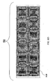
- FIG. 11B shows unsingulated leadframes after they are molded simultaneously to form molded strips 1103. After molding, portions of the DAP from each package, for example, tie bars at the four corners, are exposed.
- FIG. 11C shows the top view of a singulated leadframe package 1102 after the molding process, before cap 510 is attached.
- FIG. 11C shows the exposed tie bars of a singulated package 1102.
- Cap 510 is coupled to the exposed tie bars to form the encasing structure. Cap surfaces 580 and 585 are both not covered by molding material 120.
- TAPP-type leadframes including ground/power interposer rings coupled to tie bars or fused leads are used.
- the die attach pad with the integrated thermally and electrically conductive cap attached to it offers a variety of advantages, in addition to the advantages discussed previously. These include providing easy access to the equipotential plane of the package (including ground potential) when the cap is connected to the corresponding bond pad on the IC or the PCB; reducing moisture migration to the IC surface in non-hermetic plastic packages; and providing flexibility of adding or removing the integrated cap without requiring to change leadframe or TAPP-type package design.
Landscapes
- Lead Frames For Integrated Circuits (AREA)
- Shielding Devices Or Components To Electric Or Magnetic Fields (AREA)
Abstract
Description
- The present application claims the benefit of
U.S. Provisional Patent Application No. 60/800,433 filed on May 16, 2006 - The following patent applications of common assignee are herein incorporated by reference in their entirety:
- "Methods and Apparatus for Improved Thermal Performance and Electromagnetic Interference (EMI) Shielding in Leadframe Integrated Circuit (IC) Packages",
U.S. Patent Application No. 11/253,714, filed October 20, 2005 - "Apparatus and Method for Thermal and Electromagnetic Interference (EMI) Shielding Enhancement in Die-Up Array Packages",
U.S. Patent Publication No. 2005-0280127 A1, filed June 21, 2004 . - The invention relates generally to the field of integrated circuit (IC) device packaging technology, and more particularly to thermal enhancement and electromagnetic interference (EMI) shielding in no-lead packages for IC devices.
- Integrated circuit (IC) semiconductor chips or dies are typically mounted in or on a package that is attached to a printed circuit board (PCB) or printed wire board (PWB). The structural frame, typically made of metal or some other conductor, to which semiconductor dies are attached during the package assembly process is known as a leadframe. A leadframe is widely used in IC packages as a carrier for the IC die and as an interconnection mechanism between the die and the electrical circuits of the PCB/PWB. A leadframe can have positions allocated for housing multiple IC dies. After dies are attached to the leadframe, metal wires are used to connect the IC die bond pads to the leadframe bond pads, which are sometimes known as bond fingers. Then the positions on the leadframe where dies are located are encapsulated in a molding compound, such as thermoset epoxy. After molding, encapsulated chips are mechanically broken loose from the leadframe rails. If parts of the leadframe protrude from the package, the package is called a leaded package. In contrast, if the package leads do not substantially protrude from the leadframe footprint, then the package is called a no-lead leadframe package or simply, a no-lead package or leadless package. In a no-lead package, straight or bended leads are bent downwards and/or inwards to be mounted on a PCB/PWB substrate.
- A variation of a no-lead leadframe package has an exposed die attach pad (DAP). The exposed DAP has a solderable outer surface opposite to the die attach surface which can be solder attached to a PCB/PWB. Another alternative no-lead package is known as a Thin Array Plastic Package (TAPP), which has multiple rows of peripheral leads for wire bonding.
- Various packages with and without a leadframe have been developed and package family outlines have been standardized by the Electronic Industries Alliance (EIA), the Joint Electron Device Engineering Council (JEDEC), and the Electronic Industries Alliance of Japan (EIAJ).
- Commercially available no-lead packages have limited thermal performance and poor EMI shielding. Thus, what is needed is reduced EMI susceptibility, in combination with improved thermal and electrical performances in integrated circuit packages. Furthermore, enhanced environmental protection is also desirable for integrated circuit packages.
- The present invention is directed to methods and apparatus for improved thermal performance and EMI shielding in IC packages.
- In an aspect of the present invention, an IC device package includes a cap having opposing first and second surfaces. A first portion of the second surface of the cap has a cavity formed therein. A planar second portion of the second surface of the cap is coupled to a DAP. The DAP has a central portion, and a plurality of tie bars coupled to the central portion of the DAP. An IC die is mounted to the central portion of the DAP. The cap and the DAP form an encasing structure that substantially encloses the IC die(s).
- In another aspect of the present invention, an IC device package is assembled. A leadframe tailored for a no-lead package is formed. An IC die is attached to a central portion of the die attach pad of the leadframe. Wire bonds are coupled between the IC die and the leadframe. A cap is attached to the leadframe. A second surface of the cap includes a cavity. The cap and the leadframe form an encasing structure that substantially encloses the IC die. A molding material is applied to encapsulate the IC die. A perimeter support ring portion of the leadframe is trimmed. Portions of the leads are bent to aid coupling of the leads to a circuit board. The encasing structure spreads heat from the IC die(s) during operation. Furthermore, the encasing structure shields EMI emanating from the IC die(s) and EMI radiating toward the IC die(s) from outside the package.
According to an aspect of the invention, an integrated circuit (IC) device package is provided, comprising: - an IC die having bond pads;
- an encasing structure that substantially encloses the IC die, comprising:
- a die attach pad having a substantially planar central portion with opposing first and second surfaces, and a plurality of tie bars coupled to and extending from the central portion, wherein the first surface of the central portion of the die attach pad has the IC die mounted on, and
- a cap having a cavity and a planar rim surrounding the cavity, such that the cavity faces the IC die when the rim is attached to the die attach pad, thereby enclosing the IC die;
- a plurality of leads having lead fingers for wire bonding arranged in at least one peripheral row surrounding the die attach pad; and
- a molding material that substantially encapsulates the IC die and at least partially fills the cavity.
- at least one electrically conductive plated area patterned on the die attach pad such that the plated area is in contact with the planar rim portion of the cap.
- at least one tab protruding from the planar rim portion; and
- at least one receptacle formed in a surface of the die attach pad corresponding to the at least one tab, wherein the at least one tab is coupled with the at least one corresponding receptacle, whereby structural coupling of the cap to the die attach pad is substantially improved.
- a thermally and electrically conductive adhesive in the at least one receptacle.
- at least one wire bond that couples at least one bond pad on the IC die to the encasing structure, whereby the encasing structure is coupled to an electrical potential.
- at least one opening through the cap that is open at the outer surface and connects to the cavity.
- a heat sink coupled to the outer surface of the cap.
- a heat slug, having a first surface coupled to an exposed second surface of the central portion of the die attach pad, and a second surface configured to be coupled to a substrate including a printed circuit board and a printed wire board.
- (a) forming a leadframe from a conductive sheet of material, the leadframe comprising:
- a centrally located die attach pad having a substantially planar central portion with opposing first and second surfaces, and a plurality of tie bars coupled to and extending from the central portion,
- a plurality of leads arranged in one or more peripheral rows surrounding the die attach pad, wherein the tie bars couple the die attach pad to one or more leads, and
- a perimeter support ring corresponding to each of the peripheral lead rows transversely connecting the leads;
- (b) attaching an IC die to the central portion of the die attach pad;
- (c) coupling bond pads on the IC die to the leadframe by forming wire bonds;
- (d) coupling a cap defining a cavity facing the leadframe such that a planar rim portion of the cap surrounding the cavity is coupled to the leadframe, wherein the cap and the leadframe form an encasing structure that substantially encloses the IC die;
- (e) applying a molding material to encapsulate at least the IC die; and
- (f) trimming the perimeter support ring from the leadframe.
- (g1) prior to step (d), placing the cap and the leadframe into mold chases.
- (g2) prior to step (d), depositing a thermally and electrically conductive adhesive on a portion of the leadframe.
- (g3) prior to step (d), plating electrically conductive material on a portion of the leadframe.
- coupling a tab on the planar rim portion of the cap with a corresponding receptacle in the leadframe, whereby coupling of the cap to the leadframe is substantially improved.
- coupling a wire bond between a pad of the IC die and the leadframe, whereby the encasing structure is electrically coupled to an electrical potential.
- encapsulating a first portion of an outer surface of the cap with the molding material, whereby a second portion of the outer surface of the cap is not covered by the molding material.
- encapsulating an outer surface of the cap with the molding material.
- encapsulating a portion of the leadframe with the molding material, exposing surfaces of the leadframe to be coupled with the cap.
- (g4) forming an opening through the cap that is open at an outer surface of the cap and at a surface of the cavity.
- flowing the molding material into the cavity through the opening.
- allowing an air pressure inside of the encasing structure to be released through the opening.
- (g5) coupling a heat sink to an outer surface of the cap.
- forming one or more conductive rings coupled to the tie bars of the die attach pad.
- These and other advantages and features will become readily apparent in view of the following detailed description of the invention. Note that the Summary and Abstract sections may set forth one or more, but not all exemplary embodiments of the present invention as contemplated by the inventor(s).
- The accompanying drawings, which are incorporated herein and form a part of the specification, illustrate the present invention and, together with the description, further serve to explain the principles of the invention and to enable a person skilled in the pertinent art to make and use the invention.
- FIGs. 1A, 1B, 2A, 2B, 3A, and 3B show cross-sectional and bottom views of various types of IC packages with exposed DAP for improved thermal performance.
- FIG. 4 illustrates an example ball grid array (BGA) IC package.
- FIGs. 5A-5F show examples of caps according to embodiments of the invention.
- FIGs. 6A-6C show plan views of examples of leadframes according to embodiments of the invention.
- FIGs. 7A-7F show cross sectional views of examples of IC packages with integrated heat spreader caps according to embodiments of the invention.
- FIG. 8 shows a flowchart illustrating example steps for assembling leadframe IC packages, according to embodiments of the invention.
- FIGs. 9A-9D show plan views of examples of leadframe IC packages undergoing assembly, according to embodiments of the invention.
- FIGs. 9E-9G show side views of examples of leadframe IC packages undergoing assembly, according to embodiments of the invention.
- FIG. 10 shows a flowchart illustrating example steps for assembling leadframe IC packages in an alternative process different from FIG. 8.
- FIGs. 11A-11C illustrate an example method for attaching a cap to a leadframe after encapsulation.
- The present invention will now be described with reference to the accompanying drawings. In the drawings, like reference numbers indicate identical or functionally similar elements. Additionally, the left-most digit(s) of a reference number identifies the drawing in which the reference number first appears.
- This specification discloses one or more embodiments that incorporate the features of this invention. The disclosed embodiment(s) merely exemplify the invention. The scope of the invention is not limited to the disclosed embodiment(s). The invention is defined by the claims appended hereto.
- The embodiment(s) described, and references in the specification to "one embodiment", "an embodiment", "an example embodiment", etc., indicate that the embodiment(s) described may include a particular feature, structure, or characteristic, but every embodiment may not necessarily include the particular feature, structure, or characteristic. Moreover, such phrases are not necessarily referring to the same embodiment. Further, when a particular feature, structure, or characteristic is described in connection with an embodiment, it is understood that it is within the knowledge of one skilled in the art to effect such feature, structure, or characteristic in connection with other embodiments whether or not explicitly described.
- The present invention is directed to methods and apparatus for improving thermal performance and electromagnetic interference (EMI) shielding in integrated circuit (IC) packages. An IC die is mounted to a DAP. The IC die may be mounted in a die-up configuration, where the die is attached to a surface of the DAP that is facing away from a board (such as a PCB). The IC die may also be mounted in a die-down configuration, where the die is attached to a surface of the DAP that is facing towards the board. Wire bonds may be used to electrically connect bond pads patterned on the die to lead fingers surrounding the DAP. Note that the base region of a lead to which a wire bond is connected is referred to as a "lead finger".
- In a no-lead IC package, leads do not protrude substantially from their respective base regions. Leads are bent downwards to be mounted on a PCB/PWB, resulting in a compact footprint of the packaged IC die, sometimes referred to as an "IC chip". This type of package is called "Chip Scale Package" or CSP. CSP can be leadframe based, where the DAP and the leads are coupled as a leadframe, and one or more perimeter support rings or dam bars structurally connect the leads. This type of package is called a no-lead leadframe package. Typical examples of no-lead leadframe packages are "Leadless Plastic Chip Carrier" or LPCC, and "Micro Leadframe Package" or MLP, where there is typically a single row of peripheral terminals.
- An example of a non-leadframe based CSP is a TAPP package, which has multiple rows of peripheral leads for wire bonding. TAPP packages are assembled with a unique process that allows for multi-row peripheral outputs as well as ground or power interposer rings. The packages are extremely thin with a nominal thickness in the range of 0.7mm, and Input/Output (I/O) densities comparable with fine pitch Ball Grid Array (fpBGA) packages. Note that a modified version of a TAPP-type package can be assembled from an appropriately designed leadframe having multiple peripheral lead rows, where each of the rows have a corresponding perimeter support ring. One or more interposer ground/power rings may also be coupled to the DAP.
- A metal cap is coupled (e.g. electrically, structurally, and/or thermally connected) to the DAP to form an encasing structure. The coupling may be effected with or without the use of a thermally and/or electrically conductive adhesive, such as solder or epoxy with metal particles or flakes. In one embodiment, the cap is coupled to the tie bars attaching one or more leads to the DAP. The tie bars may be widened or fused to leads. In another embodiment, the cap is coupled to the leads. In yet another embodiment, the cap is coupled to the DAP. The cap may be coupled with any combination of DAP, leads, and tie bars. Tabs on the cap mate with matching receptacles on one or more fused leads and/or tie bars to improve coupling and overall structural strength.
- The encasing structure formed by a cap and a DAP approximates an equipotential surface, known as a "Faraday Cage", surrounding the die and the interconnections. The encasing structure material is typically a very good conductor of heat, and is relatively rigid (e.g., copper or copper alloy C151). The encasing structure may provide improved EMI shielding, improved heat transfer from the IC die, enhanced rigidity of the package, and improved environmental (e.g., mechanical shock, vibration, impact, stress, temperature, moisture, corrosion, etc.) protection.
- In one embodiment, the die and the wire bond are encapsulated in a molding material, which provides environmental protection. The molding material may also completely cover the cap. In other embodiments, the cap is partially covered, or is not covered by the molding material.
- Different families of leadframe-based leaded and no-lead packages are discussed in C. A. Harper, Electronic Packaging and Interconnection Handbook, 3rd edition, McGraw-Hill, New York, pp. 7.61-7.67, 2000, which is incorporated by reference herein in its entirety.
- Common plastic molding compound encapsulated leadframe packages (an example of which is a Plastic Quad Flat Pack or PQFP) exhibit poor thermal performance, because there is no continuous heat dissipation path between the DAP and the leads. Heat generated on the active surface of the IC die is dissipated primarily through the top and bottom surfaces of the package. The leadframe conducts some heat into a PCB/PWB to which the package is attached. The molding material that encapsulates the IC die transfers some heat to the environment through various convection paths and radiation paths. Typical molding materials have a low thermal conductivity value, such as around or between 0.2 ~ 0.9 W/m·K. Therefore, molding materials in conventional leadframe packages impose the primary bottleneck for heat dissipation from the die to the external surfaces and terminal leads of the package.
- Thermal performance of leaded and no-lead leadframe packages can be improved by exposing the DAP at the bottom surface of molding material.
- FIGs. 1A and 1B are respectively side and bottom views of a
leaded PQFP package 100 with an exposed DAP.Package 100 comprises IC die 150,DAP 140,wirebonds 130,molding material 120, adhesive 170, and package leads 180.DAP 140 and package leads 180 may be part of a leadframe. IC die 150 is mounted onDAP 140 with adhesive 170.Molding material 120 encapsulates IC die 150 and wirebonds 130.Wirebonds 130 connect the bond pads on IC die 150 to package leads 180.Additional wirebonds 130 may be formed between the IC die andDAP 140, andDAP 140 and leads 180, as shown in FIG. 1A. andDAP 140 has at least a portion of its outer surface exposed. A thermally conducting solder/adhesive coating on the exposed surface ofDAP 140bonds package 100 to a PCB/PWB 160. PCB/PWB 160 acts as a heat spreader for the package, as the heat generated on the active surface ofdie 150 is dissipated into PCB/PWB 160 with very low conductive thermal resistances. This type of package is referred to as an "Exposed Pad Thin Quad Flat Pack" or eTQFP package. - FIGs. 2A and 2B are respectively side and bottom views of a no-
lead leadframe package 200 with exposedDAP 140.Package 200 comprises IC die 150,DAP 140,wirebonds 130,molding material 120, adhesive 170, and package leads 280.DAP 140 and package leads 280 may be part of a leadframe. IC die 150 is mounted onDAP 140 with adhesive 170.Molding material 120 encapsulates IC die 150 andwire bonds 130. At least a portion of the outer surface ofDAP 140 is coated with a thermally conducting solder or adhesive, which bondspackage 200 to a PCB/PWB 160. This type of package is referred to as a "Micro Leadframe Package" or MLP, also known as a "Quad Flat No-Lead" or QFN package, as package leads 280 do not protrude substantially from the package outline. Package leads 280surround DAP 140. In a no-lead package such aspackage 200, typically, there is only one row of peripheral leads.Wire bonds 130 connect leads 280 to bond pads on IC die 150.DAP 140 may be connected to ground potential or a certain power potential. - FIGs. 3A and 3B are respectively side and bottom views of a no-lead TAPP-
type package 300 with exposedDAP 140.Package 300 comprises IC die 150,DAP 140,wirebonds 130,molding material 120, adhesive 170,interposer ring 390, and package leads 385. The outer surface ofDAP 140 is coated with a thermally conducting solder or adhesive, which bondspackage 300 to a PCB/PWB 160.Leads 385surround DAP 140 in more than one row forming an array of output leads.Wire bonds 130 connect leads 385 to corresponding bond pads on IC die 150. Having multiple rows of package leads increases I/O density of the packaged circuit. Additionally, one or more interposer rings 390 may be included in the package.Interposer ring 390 is typically coupled to ground potential. Note thatinterposer ring 390 does not necessarily have to be connected to ground. It can be connected to a certain power potential as well. TAPP packages have a unique assembly process. However, as mentioned earlier, TAPP-type packages can have a leadframe-based assembly process, if the leadframe design is modified to include interposer rings and multiple peripheral lead rows. - Though the above described packages show improvement in thermal performance, they exhibit poor electromagnetic interference (EMI) shielding. A change in the electrical current carried by a conductor results in the radiation of electromagnetic waves. Such waves propagate through space at the speed of light, and when not wanted, are called EMI. A relatively slow change in the electrical current causes a small amount of electromagnetic radiation with a long wavelength and a low frequency. A relatively rapid change in the electrical current causes a large amount of radiation with a short wavelength and a high frequency. The unwanted high frequency electromagnetic radiation is sometimes called radio-frequency interference (RFI), but in the interest of brevity, this document refers to all unwanted electromagnetic radiation as EMI, regardless of frequency.
- IC die 150 is more susceptible to higher frequency EMI. Because higher frequencies are more energetic, they may cause larger voltage swings in the metal traces on an IC die. Because modem IC gates are small in size, they operate with a low signal voltage. Thus, signal line voltage swings caused by high-frequency EMI may cause a change in logic state and may result in timing and logic failures in electronic devices.
-
Molding materials 120 are typically transparent to electromagnetic radiation. Referring to FIG. 1A, electromagnetic radiation generated bydie 150 will escape frompackage 100 and potentially interfere with the operation of nearby components. Conversely, EMI from nearby components will enterpackage 100 and may interfere with the operation ofdie 150. - Various package configurations have been considered to address the thermal and EMI issues. FIG. 4 illustrates an example BGA package having improved thermal performance, and somewhat improved EMI shielding. FIG. 4 shows a cross-sectional view of a
BGA package 400 with an IC die 150 mounted on a printedcircuit substrate 410 with adhesive 170.Wirebonds 130 and IC die 150 are encapsulated by amolding material 120. IC die 150 is electrically connected to PCB/PWB 160 throughsolder balls 430.BGA package 400 includes a drop-inheat spreader 425 to promote dissipation of heat withinmolding material 120. However, direct contact between IC die 150 andheat spreader 425 is not permitted inpackage 400. Accordingly, heat generated by IC die 150 must pass throughmolding material 120 in order to reachheat spreader 425, and may therefore remain trapped withinBGA package 400. Furthermore, drop-inheat spreader 425 only provides limited EMI shielding, if any. For example, EMI generated outsideBGA package 400 can penetrate printedcircuit substrate 410 and interfere with the operation of IC die 150. Also, EMI generated by IC die 150 can escapeBGA package 400 through trace metal openings or gaps in printedcircuit substrate 410. - Different types of heat spreader designs are discussed in various references, such as
U.S. Patent No. 5,977,626 , "Thermally and Electrically Enhanced PBGA Package," to Wang et al.,U.S. Patent No. 6,552,428 "Semiconductor Package Having An Exposed Heat Spreader" to Huang et al.,U.S. Patent Pub. No. 20030057550-A1 , entitled "Ball Grid Array Package Enhanced with a Thermal and Electrical Connector",U.S. Patent Publication No. 2005-0280127 A1 , titled "Apparatus And Method For Thermal And Electromagnetic Interference (EMI) Shielding Enhancement In Die-Up Array Packages", all of which are incorporated by reference herein in their entireties. - A variety of EMI shielding designs are also proposed in various references, such as
U.S. Patent 5,294,826 , titled "Integrated Circuit Package and Assembly Thereof for Thermal and EMI Management," andU.S. Patent 5,650,659 , titled "Semiconductor Component Package Assembly Including an Integral RF/EMI Shield", both of which are incorporated herein in their entireties. - Integrated heat spreaders used in commercially available leadframe packages are either placed against the backside of the DAP (drop-in heat spreader MQFP package, for example), or the DAP of leadframe is removed and replaced by the integrated heat spreader on which the IC die is attached. The IC die is encapsulated together with the integrated heat spreader. While the thermal performance is improved for these integrated heat spreader packages, protection against electromagnetic interference (EMI) has not been provided by the integrated heat spreaders. Additionally, the integrated heat spreaders are all structurally located on the backside of the die. To expose the integrated heat spreader on the top of the package for external heat sink attachment, die-down leadframe package must be used. If an IC die was initially packaged in a conventional die-up package and it was later decided to add a drop-in heat spreader exposed on the package top, the IC die must be redesigned in order to match the pin-out. Therefore, what is needed is a robust drop-in heat spreader integration method that provides EMI shielding of the IC die and can be used for both die-up and die-down leadframe packages.
- The present invention enables easy integration of a drop-in heat spreader to leadframe-based no-lead packages and TAPP-type no-lead packages, either in a die-up or in a die-down configuration. In the following sections, the main components of an example no-lead package, i.e. a cap, and a no-lead leadframe, are discussed in detail.
- Example embodiments for improved heat spreader cap structures are described in this section. Further embodiments will become apparent to persons having skill in the relevant art(s) from the teachings herein. Elements of the embodiments described herein can be combined in any manner.
- FIG. 5A illustrates a cross sectional view of a
cap 510. FIG. 5B illustrates a bottom view ofcap 510, in accordance with an embodiment of the present invention.Cap 510 may be incorporated into various integrated circuit packages, such as shown in FIGS. 7A-7F, which are described in detail below. The packages may incorporate leadframes, such as shown in FIGs. 6A - 6C, which are described in detail below. -
Cap 510 has atop portion 590, asidewall portion 592, and arim 594 extending around a bottom periphery ofcap 510. It should be noted that references to "top" and "bottom" are merely exemplary for the convenience of description. It is not intended that this invention be limited to any particular spatial orientation. -
Sidewall portion 592 couples (e.g., electrically, structurally, and thermally)top portion 590 torim 594. Further,sidewall portion 592 is angled outward fromtop portion 590. Although FIG. 5A illustrates a planartop portion 590,top portion 590 can be non-planar (e.g., curved, concave, convex, hemispherical, or other shapes). Additionally, although FIGs. 5A and 5B illustrate an angled-outward sidewall portion 592,sidewall portion 592 may be perpendicular to or angled inward fromtop portion 590. Furthermore,sidewall portion 592 is not limited to a linear cross-section and may employ other cross-sectional shapes such as convex inward and outward as would be understood by one skilled in the art. -
Cap 510 further has a first surface 580 (outer surface) and a second surface 585 (inner surface).Second surface 585 forms an upper boundary of acavity 570 in a bottom portion ofcap 510.Rim 594 surroundscavity 570.Cavity 570 is shown in FIG. 5A as having a trapezoidal cross section, but may have other shapes (e.g., square, rectangular, irregular, etc.). Although FIG. 5B illustratescavity 570 having a circular shape,cavity 570 may have other shapes. Further,cap 510 may have various shapes such as round, rectangular, square, elliptical, oval, or any other shape. - In
cap 510,rim 594 may have a substantially planar lip portion. The bottom surface of the lip portion ofrim 594 has one or moreprotruding tabs 515a-e.Tabs 515a-e may have any shape. For example, FIGS. 5A and 5B show afrustum tab 515a, aconical tab 515b, apair 517 ofconical tabs tab 515e.Cap 510 is not limited to the shapes, sizes, locations, or numbers oftabs 515 shown.Cap 510 may also have zero or more tabs of any shape, of any size, in any locations. - The outer periphery dimension of
cap 510 is preferably the same size as the periphery, or smaller than the periphery of the substantially planar area enclosed by the peripheral row of leads to facilitate visual inspection of lead interconnect on the PCB/PWB. In an alternative embodiment, the outer periphery dimension ofcap 510 extends beyond the periphery of the substantially planar area enclosed by the peripheral row of leads. For manufacturing considerations, the outer periphery ofcap 510 is preferably smaller than the dimension of a leadframe perimeter support ring 630 (e.g., see FIG. 6A, further described below). Althoughcap 510 is illustrated having a particular size, other sizes may be used, as would be understood by persons skilled in the relevant art(s). - In one embodiment,
cap 510 may be configured to mount an external heat sink. In another embodiment,cap 510 may be configured to be thermally and/or electrically connected to a PCB/PWB. -
Cap 510 may be made of a thermally conductive material and/or an electrically conductive material, such as a metal. For example, the material forcap 510 may include copper, a copper alloy, (e.g., C194, C151, C7025, or EFTEC 64T), aluminum, an aluminum alloy, ferromagnetic materials, laminated copper or iron, etc. Other metals and combinations of metals/alloys, or other thermally and electrically conductive materials (e.g., ceramics, metallized plastics, laminated metal foils on plastic or ceramic, etc.) could also be used.Cap 510 andDAP 140 may be made of the same material or different materials. Whencap 510 andDAP 140 are made of the same material, or materials having the same coefficient of thermal expansion, structural integrity may be improved, such as reducing thermal stress on the die (sandwiched between the cap and leadframe). Furthermore,cap 510 may have any thickness, depending on the particular application. For example,cap 510 may have a thickness of 0.1 to 0.5 mm. Alternatively,cap 510 may have a thickness of less than 1.0 mm. - The bottom surface of the lip portion of
rim 594 may be fully or partially coated or laminated with a layer of dielectric material (e.g. solder mask, dielectric film etc.). In this manner, the shorting of leads after assembly may be prevented. - In one embodiment, the cap may have openings through the
first surface 580 and thesecond surface 585. For example, FIGS. 5C and 5D show example caps 511 having openings orslots 520 formed insidewall portions 592. Although FIGs. 5C and 5D illustrateslots 520 insidewall portion 592 as rectangular or trapezoidal,slots 520 can have other shapes. - In another embodiment, a
cap 512 may have holes/openings 530 intop portion 590 as illustrated in FIG. 5E.Cap 512 may have any number of holes. Furthermore, holes 530 can have any shape. -
Holes 530 incap 512 andslots 520 incap 511 allow the flow ofmolding material 120 intocavity 570 during a manufacturing process. Additionally or alternatively,slots 520 andholes 530 may release pressure buildup (during or after manufacture) occurring incavity 570. Becausesmaller holes 530 andslots 520 may require a higher pressure to flow or injectmolding material 120. intocavity 570,larger holes 530 andslots 520 may be desirable from a manufacturing perspective. However, it may be required that the size ofholes 530 andslots 520 to be limited to reduce EMI penetration. Ahole 530 or slot 520 diameter may be in the range of 0.5 - 3.0 mm. A diameter of 1.5 mm may be used to shield against EMI having a highest harmonic frequency of about 10 GHz. An outer surface ofcap 510 may be completely or partially encapsulated inmolding material 120, or may have nomolding material 120 covering it. - As shown in FIG. 5F, a thermally
conductive spacer 586 may be attached to the inside surface (second surface 585) ofcap 510+ to reduce the space between the heat spreader cap and the top surface of IC die 150.Spacer 586 may also be attached to the top surface of IC die 150 in the center region away from the peripheral bond pads on IC die 150. The thermally conductive spacer may be of any shape and made of any material including copper, aluminum, metal alloy, silicon etc.Cap 510+ may hang unattached to the DAP, the DAP's extensions (such as the tie bars), or the package leads, when supported byspacer 586 connected to IC die 150. - Example embodiments for leadframe structures are described in this section. As mentioned before, no-lead packages may or may not be leadframe-based. Further embodiments will become apparent to persons having skill in the relevant art(s) from the teachings herein. Elements of the leadframe embodiments described herein can be combined in any manner.
- FIGs. 6A-6C illustrate various leadframe structures. FIG. 6A shows a
leadframe 600 having aDAP 604 with acentral portion 605, and a plurality of tie bars 620.Leadframe 600 also includes a plurality ofleads 607, and aperimeter support ring 630. DAPcentral portion 605 may be similar toexposed DAP 140 in FIG. 1A. In FIG. 6A,leadframe 600 is rectangular in shape, having a rectangularperimeter support ring 630 surrounding its periphery.Perimeter support ring 630 includes a first perimeter edge ordam bar 634a, a second perimeter edge ordam bar 634b, a third perimeter edge ordam bar 634c, and a fourth perimeter edge ordam bar 634d, coupled in a rectangular ring. Note,dam bars 634a-634b may be individual bars which may or may not be coupled in a ring. DAPcentral potion 605 is centered inleadframe 600. DAPcentral portion 605 may be rectangular in shape. In the embodiment of FIG. 6A, tie-bars 620 extend outward from the four corners of DAPcentral portion 605. -
Leads 607 extend inward perpendicularly fromperimeter support ring 630. Leads 607a-h are coupled to tie bars 620.Lead 607a is coupled betweenedge 634a ofleadframe 600 andtie bar 620a.Lead 607b is coupled betweenedge 634a ofleadframe 600 andtie bar 620b.Lead 607c is coupled betweenedge 634b ofleadframe 600 andtie bar 620b.Lead 607d is coupled betweenedge 634b ofleadframe 600 andtie bar 620c.Lead 607e is coupled betweenedge 634c ofleadframe 600 andtie bar 620c.Lead 607f is coupled betweenedge 634c ofleadframe 600 andtie bar 620d.Lead 607g is coupled betweenedge 634d ofleadframe 600 andtie bar 620d.Lead 607h is coupled betweenedge 634d ofleadframe 600 andtie bar 620a.Leads 607 are supported byperimeter support ring 630 inleadframe 600. Leads 607 (exceptleads 607a-h) may have a portion withinperimeter support ring 630 that are generally oriented radially with respect to a center ofleadframe 600. - Although FIGs. 6A-6C illustrate a square leadframe, DAP
central portion 605, andperimeter support ring 630, other shapes could also be employed (e.g., rectangle, circle, ellipse, curvilinear rectangle, etc). Furthermore, the number ofleads 607 is not limited by FIG. 6A, and leadframes may have any number of leads 607. - FIG. 6B shows one
embodiment 601 ofleadframe 600. Tie-bar 620 may be widened, and may be located at other positions around DAPcentral portion 605 than what is shown in FIG. 6B. Any number ofleads 607 may be fused to a tie-bar, which may further effectively widen the tie-bar. FIG. 6B shows a tie-bar 640 coupled between DAPcentral portion 605 and first andsecond leads Leadframe 601 may have one or more fused tie bar leads 620, widened fused leads 640, or both. Alternatively,leadframe 601 may have neither widened fused leads 640 nor fused tie-bar leads 620. Furthermore, as shown in FIG. 6B,leadframe 601 may have one or more tie bars 610 that are not coupled to leads 607. - In another
embodiment 602 illustrated in FIG. 6C, tie-bars 620a-d havereceptacles 615 formed therein.Receptacles 615 correspond totabs 515 formed in cap 510 (shown in FIG. 5A). As withtabs 515,receptacles 615 can include a rectangular shaped receptacle 615a, apair 617 of conical shapedreceptacles pair 619 ofrounded receptacles receptacles 615 are not limited to these shapes, combinations of shapes, numbers, locations, or sizes.Receptacles 615 may be indentions (not fully penetrating the leadframe 602) or may be cut-outs (fully penetrating the leadframe 602).Leadframe 602 may have any number ofreceptacles 615 of any size, shape, and locations.Receptacles 615 onleadframe 602 are configured to couple withtabs 515 oncap 510 providing increased structural strength, as well as enhanced thermal and electrical connection. - Example materials for leadframe include metals, such as copper, copper alloy, (e.g., C194, C151, C7025, or EFTEC 64T), aluminum, aluminum alloys, ferromagnetic materials, other metals and combinations of metals/alloys, or other thermally and electrically conductive materials.
Cap 510 andleadframe 600 may be made of the same material or different materials.Leadframe 600 may be any thickness depending on the particular application. For example,leadframe 600 thickness may range from 0.05mm to 0.5mm. In another embodiment,leadframe 600 is less than 1.17mm thick. - In one embodiment,
leadframe 600 provides stiffening and/or structural support to an IC package. In another embodiment,leadframe 600 provides heat spreading to an IC package. In another embodiment,leadframe 600 is electrically conductive, and can act as a power or ground plane for an IC package.Leadframe 600 can be configured to provide any combination of stiffening, heat spreading, and electrical conductivity, as required by the particular application. - Example embodiments for IC packages are described in this section. Further embodiments will become apparent to persons having skill in the relevant art(s) from the teachings herein. Elements of the IC package embodiments described herein can be combined in any manner.
- FIG. 7A shows an
example IC package 702 mounted on PCB/PWB 160.Package 702 comprises IC die 150,wirebonds 130,molding material 120, adhesive 170,leadframe 600, andcap 510.Leadframe 600 comprises DAPcentral portion 605, tie bars 620 (not shown in this view), and leads 607. IC die 150 is mounted on DAPcentral portion 605 in a die-up configuration.Cap 510 faces die 150.Leadframe 600 andcap 510 form anencasing structure 720 that substantially encloses IC die 150, providing improved structural integrity, EMI shielding, thermal performance, and environmental (e.g., mechanical shock, vibration, caustic, moisture, and radiation) protection. Note that additional IC dies and/or other electrical components may be attached to DAPcentral portion 605. -
Cap 510 andleadframe 600 may be made of copper or copper alloys. The thermal conductivity of copper (roughly 390 W/m·K) is much greater than for typical molding materials 120 (0.2 - 0.9 W/m·K). Therefore, the heat generated bydie 150 is conducted through adhesive 170 to DAPcentral portion 605 and out of the package through tie bars 620 (not shown in FIG. 7A), package leads 607 andcap 510. Also, sincecap 510 andleadframe 600 are electrically connected, they may form a near-equipotential surface, such that encasingstructure 720 approximates an ideal "Faraday Cage". In this manner, die 150 is isolated from external EMI. Additionally, external devices are also shielded from EMI generated bydie 150. Since copper and copper alloys have a much higher modulus of elasticity (about 125 GPa) compared to a typical cured plastic molding compound used for molding material 120 (about 25 GPa), copper embodiments of the present invention provide improved structural rigidity and environmental protection. - In one embodiment,
cap 510 andleadframe 600 are coupled together without the use of tabs and receptacles. In another embodiment, as shown in FIG. 7A,cap 510 hastabs 515 which fit corresponding receptacles (similar toreceptacle 615, not shown in this view) onleadframe 600.Tabs 515 and corresponding receptacles onleadframe 600 may facilitate tight lock-in of thecap 510 toleadframe 600. Further, the configuration oftabs 515 and corresponding receptacles onleadframe 600 are such thatcap 510 mates correctly withleadframe 600 in only one orientation, which may facilitate assembly. Note that in an alternative embodiment,cap 510 may have receptacles that interlock with tabs ofleadframe 600. - Thermally and/or electrically conductive adhesive materials (e.g., epoxy filled with silver flakes or other conductive particles) may be used to improve the coupling between
cap 510 andleadframe 600. An adhesive material can be used to attach atab 515 and a corresponding receptacle onleadframe 600, when they are present. Alternatively, the adhesive material may be used at areas wherecap 510 contacts leadframe 600. Tin-lead or silver soldering materials can be used to joincap 510 withleadframe 600 through processes such as solder plating and reflow or screen printing of solder paste and reflow. In another embodiment, welding or other metal joining methods can be used to attachcap 510 toleadframe 600. -
Leadframe 600 may be plated with a conductive material to improve the thermal and electrical connection. In one embodiment,cap 510 may be mounted to DAPcentral portion 605 ofleadframe 600. In another embodiment,cap 510 is mounted to tie-bars 620 coupled between DAPcentral portion 605 and the package leads 607. In yet another embodiment, as shown in FIG. 7A,cap 510 may be mounted to one or more leads 607.Cap 510 can be mounted to any combination of DAPcentral portion 605, tie bars 620, and leads 607. Further, portions of the bottom surface, or all of the bottom surface ofrim 594 ofcap 510 may be coated with a layer of dielectric material (e.g. solder mask, dielectric film etc.) to prevent electrical shorting with one or more ofleads 607. In one embodiment,cap 510 may not be in physical contact withleadframe 600. In yet another embodiment, the contact surface betweencap 510 andleadframe 600 may be substantially flat and smooth when welding or other metal joining method is used to couplecap 510 toleadframe 600. -
Leads 607 ofleadframe 600 are shaped to be coupled to a PCB/PWB 160. For example, an outer portion ofleads 607 extending frompackage 702 may be bent downward to allowleads 607 to contact a PCB/PWB 160. - Integrating a molding material, such as glob top or plastic molding compound, with an encasing structure may enhance the structural rigidity and planarity of the IC package. For example, the combination of the molding material and the encasing structure may reduce IC die cracking and delamination. Integrating the molding material with the encasing structure also enhances environmental protection. For example, the integrated package can provide protection against mechanical stress, impact, vibration, chemical corrosives, moistures, heat exposure, radiation, etc.
- Additionally, attaching the IC die directly to the encasing structure adds mass to the die support, and helps reduce microphonics. The metal traces of the IC die have electrical resistance, capacitance, and inductance. After IC packaging and assembly of the package on the PCB/PWB, the IC die is under mechanical stress. Vibration, mechanical shock, or sudden change of temperature can cause a change of stress distribution within the IC die, and thus alter a capacitance and resistance such that a voltage vibration or drift is produced. This phenomenon is called microphonics. Attachment of the semiconductor die directly to the encasing structure increases the mass and helps dampening these mechanical shocks and vibrations, thus reducing microphonics.
- Typical molding materials, such as plastic molding compound, have low thermal conductivity (e.g., about 0.2 to 0.9 W/m·K) and therefore create a bottleneck for heat dissipation in conventional IC packages. The encasing structure may eliminate this bottleneck by providing a thermally conductive path from the bottom surface of the IC die to the outer surfaces of the package. Additionally, the encasing structure is made with materials that have high thermal conductivity (e.g., approximately 390 W/m·K for copper) and therefore promote heat dissipation.
- An encasing structure formed by
cap 510 andleadframe 600 may be incorporated into IC packages of many different configurations. FIGs. 7A-7F illustrate some example embodiments of the present invention, each showing an encasing structure. For example,cap 510 is coupled withleadframe 600 to form encasingstructure 720 in FIG. 7A. Encasingstructure 720 substantially encloses IC die 150. In the packages shown in FIGs. 7A-7F, at least onewire bond 130 couples at least one bond pad (not shown) on a surface of IC die 150 toleadframe 600. The IC bond pad connected to leadframe 600 may be a ground pad. - As shown in FIG 7A,
cap 510 has atop surface 590 that is exposed through themolding material 120encapsulating package 702. Thus,molding material 120 does not cover the entirety of first surface 580 (outer surface of cap 510). Second surface 585 (inner surface of cap 510) is covered bymolding material 120. -
Package 704 in FIG. 7B andpackage 706 in FIG. 7C are similar topackage 702 in FIG. 7A, but showing the relative position of tie bars 620 (not shown in FIG. 7A) with respect toleads 607 inleadframe 600. FIG. 7B shows thatleadframe 600 may have tie bars 620 on the same plane as the leads ofleads 607. Tie bars may also be in a different plane with respect to leads. As shown in FIG. 7C, tie bars 621 are above leads 607. - FIG. 7D shows an
IC package 708 similar topackage 702 in FIG. 7A. However, inIC package 708,cap 510 is configured to mount anexternal heat sink 701.Leadframe 600 andcap 510 provide a path for heat to be conducted fromdie 150 toheat sink 701, and thus out ofpackage 708. Inpackage 708, first andsecond surfaces cap 510 are not fully covered bymolding material 120. InIC package 708,cap 510 is added to the package after moldingmaterial 120 has been applied during the assembly process. - A
package 710, similar topackage 702, may include acap 511 instead ofcap 510 with no openings.Cap 511 has one or more openings (e.g. slots 520), as shown in FIG. 7E. These openings may act as mold gate openings, allowingmolding material 120 to flow or be injected intocavity 570. Inpackage 710, bothfirst surface 580 andsecond surface 585 ofcap 511 are covered bymolding material 120. - FIG. 7F shows a
package 712, which is the equivalent TAPP-version ofpackage 702 shown in FIG. 7A. As characteristic of TAPP-type packages, leads 385 are arranged aroundDAP 140 in an array containing multiple rows rather than a single peripheral row.Wire bonds 130 are formed to connect bond pads onIC 150 to leads 385.Cap 510 may be attached to the outermost row ofleads 385 withtabs 515. One or more interposer rings 390 may be present surroundingDAP 140.Cap 510 andDAP 140 may be part of an encasing structure that encloses IC die 150. In one embodiment,DAP 140,interposer ring 390, and leads 385 may be coupled together as a leadframe. Variation in package structure discussed with reference to FIGs. 7B-7E are applicable toTAPP package 712 as well. - Embodiments of the present invention are not restricted to die-up configurations. A package may be in a die-down configuration, according to an example embodiment of the present invention. In comparison to package 702 in FIG. 7A,
surface 580 ofcap 510 may be exposed on the bottom side of a package. The features reflected in the embodiments illustrated in FIGs. 7A - 7F are applicable to the die-down configurations as well. In a die-down package, exposedsurface 580 ofcap 510 may be coupled to PCB/PWB 160 with electrically and/or thermally conductive adhesive or solder. Thus, heat conducted from IC die 150 throughleadframe 600 andcap 510 may be conducted out of the package into PCB/PWB 160.Surface 580 ofcap 510 may be electrically connected to a power pad or pads on PCB/PWB 160 to improve EMI shielding and power delivery from the package. Alternatively,surface 580 ofcap 510 may be electrically connected to ground pad or pads on PCB/PWB 160 to improve EMI shielding and current return from the package. A thermal and/or electrical connector, such as a heat slug may be attached to theouter surface 580 ofcap 510 in a die-down configuration, wherein the heat slug couples the package to the PCB/PWB. - FIG. 8 shows a
flowchart 800 illustrating example steps to assembleleadframe package 702 shown in FIG. 7A, according to one embodiment of the present invention. As would be understood by one skilled in the art, adaptation of these assembly processes could be used to assemble any embodiments, including those illustrated in FIGs. 7A-7F. The steps in FIG. 8 do not necessarily have to occur in the order shown, as will be apparent to persons skilled in the relevant art(s) based on the teachings herein. Other operational and structural embodiments will be apparent to persons skilled in the relevant art(s) based on the following discussion. These steps are described in detail below with respect to FIGS. 9A-9G, for illustrative purposes. FIGs. 9A-9D illustrate top views and FIGs. 9E-9G show side views of embodiments of the invention at different stages of assembly. -
Flowchart 800 begins withstep 805. Instep 805, a leadframe is formed from a sheet of material. Example leadframe material and features are discussed elsewhere herein. - In
step 810, at least one IC die is attached to a DAP of a leadframe. - In
step 815, wire bond interconnection is performed. - In
step 820, a cap is attached to the leadframe. - In
step 825, the package is encapsulated. - In
step 830, the leadframe perimeter support ring is trimmed. - In
step 870, individual packages are singulated, i.e. cut out from the leadframe panel. - FIG. 9A illustrates a view of a
single leadframe 600. Note thatleadframe 600 in FIG. 9A-9G may have features described inleadframe embodiments - FIG. 9B illustrates an
example leadframe panel 900 that contains an array ofleadframes 600.Leadframes 600 inleadframe panel 900 are manufactured by an etching or stamping process, for example. - FIG. 9C shows a partially assembled
package 910. At least one IC die 150 is attached to DAPcentral portion 605.Wirebonds 130 are used to attach pads of IC die 150 toleadframe 600, providing electrical connections from IC die 150 toleads 607, tie bars 620, and/or DAPcentral portion 605. Acap 510 is attached toleadframe 600. Electrically and/or thermally conductive adhesive materials may be used to improve coupling betweencap 510 andleadframe 600.Cap 510 andleadframe 600 are joined to form an encasing structure which substantially encloses IC die 150. Cavity size ofcap 510 should be large enough to avoidcap 510 touching the bond wires. - FIG. 9D illustrates a partially assembled
panel 920 of partially assembled packages 910. - FIG 9E shows the side view of a partially assembled package after
step 815 offlowchart 800 is finished. - FIG. 9F shows the side view of partially assembled
panel 920 of FIG. 9D, afterstep 820 offlowchart 800. - FIG. 9G shows a side view of an encapsulated
panel 930 of leadframe packages, afterstep 825 offlowchart 800. Instep 825, the package is encapsulated. In this step, amolding material 120 encapsulates partially assembled packages 910.Packages 910 may be clamped in a mold chase to mold or shape a molding compound being used to encapsulate the package. As described elsewhere herein, an outer peripheral dimension of acap 510 is smaller than a peripheral dimension ofperimeter support ring 630. This prevents the molding material from bleeding through gaps between leads 607.Support ring 630 may also provide sealing between the clamped mold chase during the transfer molding process. - Leadframe
perimeter support ring 630 is trimmed instep 830.Leads 607 are ready to be formed into contact pins for board mount and a leadframe package is completely assembled. For example, the outer portion ofleads 607 extending from the package may be bent downward to allow them to contact a PCB/PWB. - In
step 870, individual packages, such aspackage 702 of FIG. 7A, are cut out from the leadframe panel. -
Flowchart 1000 shown in FIG. 10 shows example steps for forming an integrated circuit package, according to an alternative embodiment of the present invention.Steps flowchart 800 in FIG. 8. However, step 1055 (placing a leadframe in the mold chase), step 1060 (placing a cap in the mold chase), and step 1070 (completing encapsulation) may be different fromflowchart 800. - According to the assembly process shown in
flowchart 1000, instead of coupling acap 510 to aleadframe 600 outside of the mold chase, aleadframe 600 and acap 510 are put into the mold chase insteps Leadframe 600 is clamped between upper and lower mold chase and contact between the cap placed in mold chase and the leadframe tie-bar or fused lead is made by clamping the cap against the leadframe. To enhance electrical contact between the cap and the leadframe, electrically conductive adhesives such as silver flake/particle loaded epoxies can be pre-deposited on the contact pads of leadframe before clamping the components on the mold chase. - In
step 1065, package encapsulation is completed. - The subsequent assembly steps in
flowchart 1000 are similar toflowchart 800. - Leadframe
perimeter support ring 630 is trimmed instep 830. - In
step 870, individual packages are singulated, i.e. cut out from the leadframe panel. - FIGs. 11A-11C illustrate how a package 1101 (similar to
package 708 in FIG 7D, but without the external heat sink 701) can be assembled following another assembly process different from the ones discussed inflowcharts central portion 605 after the molding step. FIG. 11A is the side view of a fully assembledsingulated package 1101. FIG. 11B shows unsingulated leadframes after they are molded simultaneously to form molded strips 1103. After molding, portions of the DAP from each package, for example, tie bars at the four corners, are exposed. FIG. 11C shows the top view of asingulated leadframe package 1102 after the molding process, beforecap 510 is attached. FIG. 11C shows the exposed tie bars of asingulated package 1102.Cap 510 is coupled to the exposed tie bars to form the encasing structure. Cap surfaces 580 and 585 are both not covered bymolding material 120. - Note that a similar assembly processes can be utilized when, instead of conventional leadframe, TAPP-type leadframes including ground/power interposer rings coupled to tie bars or fused leads are used.
- The die attach pad with the integrated thermally and electrically conductive cap attached to it offers a variety of advantages, in addition to the advantages discussed previously. These include providing easy access to the equipotential plane of the package (including ground potential) when the cap is connected to the corresponding bond pad on the IC or the PCB; reducing moisture migration to the IC surface in non-hermetic plastic packages; and providing flexibility of adding or removing the integrated cap without requiring to change leadframe or TAPP-type package design.
- While various embodiments of the present invention have been described above, it should be understood that they have been presented by way of example only, and not limitation. It will be apparent to persons skilled in the relevant art that various changes in form and detail can be made therein without departing from the spirit and scope of the invention. Thus, the breadth and scope of the present invention should not be limited by any of the above-described exemplary embodiments, but should be defined only in accordance with the following claims and their equivalents.
Advantageously, the encasing structure spreads heat from the IC die during operation of the IC die.
Advantageously, the encasing structure shields electromagnetic interference (EMI) emanating from the IC die and EMI radiating toward the IC die from outside the package.
Advantageously, the die attach pad, and the plurality of leads are coupled as a leadframe, wherein one or more perimeter support rings or dam bars structurally connect the leads.
Advantageously, the leads are arranged in an array with more than one row.
Advantageously, the package further comprises one or more interposer conducting rings coupled to the tie bars surrounding the die attach pad.
Advantageously, the die attach pad, the interposer rings, and the plurality of leads are coupled as a leadframe, wherein one or more perimeter support rings or dam bars structurally connect the leads.
Advantageously, the rim of the cap includes a substantially planar lip portion extending outwards from the cavity that encloses the IC die.
Advantageously, the cap is in electrical and thermal contact with at least one lead.
Advantageously, the cap is electrically isolated from any of the plurality of leads.
Advantageously, at least a portion of the planar rim of the cap is coated with a dielectric material.
Advantageously, at least a portion of the die attach pad coupled to the cap is coated with a dielectric material.
Advantageously, at least one of the plurality of tie bars is wider relative to others of the plurality of tie bars.
Advantageously, at least one of the plurality of leads is wider relative to others of the plurality of leads.
Advantageously, the cap is in electrical and thermal contact with at least one tie bar.
Advantageously, the plurality of tie bars and the plurality of leads are positioned in a first plane.
Advantageously, the plurality of tie bars are positioned in a first plane and the plurality of leads are positioned in a second plane.
Advantageously, the planar rim portion of the cap is coupled to the die attach pad by a thermally and electrically conductive adhesive.
Advantageously, the package further comprises:
Advantageously, the cap is coupled to a ground potential.
Advantageously, the cap is coupled to a power potential.
Advantageously, the package further comprises:
Advantageously, a tab is positioned on a corner of the planar rim portion.
Advantageously, the at least one corresponding receptacle has an opening, indentation, or edge cutout configuration.
Advantageously, the at least one tab and the at least one corresponding receptacle are configured to facilitate coupling the cap to the die attach pad in a predetermined orientation.
Advantageously, the package further comprises:
Advantageously, the cap has an outer surface that opposes the cavity, wherein a first portion of the outer surface is covered by the molding material, and wherein a second portion of the outer surface of the cap is not covered by the molding material.
Advantageously, the molding material further encapsulates an outer surface of the cap that opposes the cavity.
Advantageously, the cap has an outer surface that opposes the cavity, wherein the cap further comprises:
Advantageously, the at least one opening through the cap is configured to facilitate release of an air pressure inside of the encasing structure.
Advantageously, a peripheral dimension of the cap substantially coincides with a peripheral dimension of the substantially planar area enclosed by the peripheral row of leads.
Advantageously, a peripheral dimension of the cap is within a peripheral dimension of the substantially planar area enclosed by the peripheral row of leads.
Advantageously, a peripheral dimension of the cap exceeds a peripheral dimension of the substantially planar area enclosed by the peripheral row of leads.
Advantageously, the cap has an outer surface that opposes the cavity, further comprising:
Advantageously, the package further comprises a thermally and electrically conductive adhesive coupling the outer surface of the cap to the substrate.
Advantageously, the second surface of the central portion of the die attach pad is exposed to be coupled to a substrate including a printed circuit board and a printed wire board.
Advantageously, the package further comprises a thermally and electrically conductive adhesive coupling the die attach pad to the substrate.
Advantageously, the package further comprises:
Advantageously, the encasing structure and the molding material provide damping against mechanical shock and vibrations.
Advantageously, the cap and the die attach pad are made of similar material including metal, metallic alloy, ferromagnetic material, and metallized polymer.
Advantageously, the cap and the die attach pad are made of dissimilar materials.
According to an aspect of the invention, a method is provided of assembling an integrated circuit (IC) device package, comprising:
Advantageously, step (e) further comprises:
Advantageously, step (a) further includes:
Claims (10)
- An integrated circuit (IC) device package, comprising:an IC die having bond pads;an encasing structure that substantially encloses the IC die, comprising:a die attach pad having a substantially planar central portion with opposing first and second surfaces, and a plurality of tie bars coupled to and extending from the central portion, wherein the first surface of the central portion of the die attach pad has the IC die mounted on, anda cap having a cavity and a planar rim surrounding the cavity, such that the cavity faces the IC die when the rim is attached to the die attach pad, thereby enclosing the IC die;a plurality of leads having lead fingers for wire bonding arranged in at least one peripheral row surrounding the die attach pad; anda molding material that substantially encapsulates the IC die and at least partially fills the cavity.
- The package of claim 1, wherein the package is in a die-up or die-down configuration.
- The package of claim 1, wherein the encasing structure spreads heat from the IC die during operation of the IC die.
- The package of claim 1, wherein the encasing structure shields electromagnetic interference (EMI) emanating from the IC die and EMI radiating toward the IC die from outside the package.
- The package of claim 1, wherein the die attach pad, and the plurality of leads are coupled as a leadframe, wherein one or more perimeter support rings or dam bars structurally connect the leads.
- The package of claim 1, wherein the leads are arranged in an array with more than one row.
- The package of claim 6, further comprising one or more interposer conducting rings coupled to the tie bars surrounding the die attach pad.
- A method of assembling an integrated circuit (IC) device package, comprising:(a) forming a leadframe from a conductive sheet of material, the leadframe comprising:a centrally located die attach pad having a substantially planar central portion with opposing first and second surfaces, and a plurality of tie bars coupled to and extending from the central portion,a plurality of leads arranged in one or more peripheral rows surrounding the die attach pad, wherein the tie bars couple the die attach pad to one or more leads, anda perimeter support ring corresponding to each of the peripheral lead rows transversely connecting the leads;(b) attaching an IC die to the central portion of the die attach pad;(c) coupling bond pads on the IC die to the leadframe by forming wire bonds;(d) coupling a cap defining a cavity facing the leadframe such that a planar rim portion of the cap surrounding the cavity is coupled to the leadframe, wherein the cap and the leadframe form an encasing structure that substantially encloses the IC die;(e) applying a molding material to encapsulate at least the IC die; and(f) trimming the perimeter support ring from the leadframe.
- The method of claim 8, wherein steps (d) and (e) are performed concurrently, and further comprising:(g1) prior to step (d), placing the cap and the leadframe into mold chases.
- The method of claim 8, further comprising:(g2) prior to step (d), depositing a thermally and electrically conductive adhesive on a portion of the leadframe.
Applications Claiming Priority (2)
| Application Number | Priority Date | Filing Date | Title |
|---|---|---|---|
| US80043306P | 2006-05-16 | 2006-05-16 | |
| US11/480,579 US8183680B2 (en) | 2006-05-16 | 2006-07-05 | No-lead IC packages having integrated heat spreader for electromagnetic interference (EMI) shielding and thermal enhancement |
Publications (2)
| Publication Number | Publication Date |
|---|---|
| EP1858080A2 true EP1858080A2 (en) | 2007-11-21 |
| EP1858080A3 EP1858080A3 (en) | 2008-11-05 |
Family
ID=38374435
Family Applications (1)
| Application Number | Title | Priority Date | Filing Date |
|---|---|---|---|
| EP20060026677 Withdrawn EP1858080A3 (en) | 2006-05-16 | 2006-12-22 | No-lead ic packages having integrated heat spreader for electromagnetic interference (emi) shielding and thermal enhancement |
Country Status (4)
| Country | Link |
|---|---|
| US (1) | US8183680B2 (en) |
| EP (1) | EP1858080A3 (en) |
| CN (1) | CN101106111B (en) |
| TW (1) | TWI388047B (en) |
Cited By (1)
| Publication number | Priority date | Publication date | Assignee | Title |
|---|---|---|---|---|
| EP2450951A1 (en) * | 2010-11-08 | 2012-05-09 | Samsung Electronics Co., Ltd. | Quad flat package with exposed paddle |
Families Citing this family (47)
| Publication number | Priority date | Publication date | Assignee | Title |
|---|---|---|---|---|
| US7271479B2 (en) * | 2004-11-03 | 2007-09-18 | Broadcom Corporation | Flip chip package including a non-planar heat spreader and method of making the same |
| US7968377B2 (en) * | 2005-09-22 | 2011-06-28 | Stats Chippac Ltd. | Integrated circuit protruding pad package system |
| US7582951B2 (en) | 2005-10-20 | 2009-09-01 | Broadcom Corporation | Methods and apparatus for improved thermal performance and electromagnetic interference (EMI) shielding in leadframe integrated circuit (IC) packages |
| US7714453B2 (en) | 2006-05-12 | 2010-05-11 | Broadcom Corporation | Interconnect structure and formation for package stacking of molded plastic area array package |
| US9299634B2 (en) * | 2006-05-16 | 2016-03-29 | Broadcom Corporation | Method and apparatus for cooling semiconductor device hot blocks and large scale integrated circuit (IC) using integrated interposer for IC packages |
| US20070273023A1 (en) * | 2006-05-26 | 2007-11-29 | Broadcom Corporation | Integrated circuit package having exposed thermally conducting body |
| US7808087B2 (en) * | 2006-06-01 | 2010-10-05 | Broadcom Corporation | Leadframe IC packages having top and bottom integrated heat spreaders |
| US9013035B2 (en) * | 2006-06-20 | 2015-04-21 | Broadcom Corporation | Thermal improvement for hotspots on dies in integrated circuit packages |
| US8581381B2 (en) | 2006-06-20 | 2013-11-12 | Broadcom Corporation | Integrated circuit (IC) package stacking and IC packages formed by same |
| US8169067B2 (en) * | 2006-10-20 | 2012-05-01 | Broadcom Corporation | Low profile ball grid array (BGA) package with exposed die and method of making same |
| US20080111219A1 (en) * | 2006-11-14 | 2008-05-15 | Gem Services, Inc. | Package designs for vertical conduction die |
| US8183687B2 (en) * | 2007-02-16 | 2012-05-22 | Broadcom Corporation | Interposer for die stacking in semiconductor packages and the method of making the same |
| US9466545B1 (en) * | 2007-02-21 | 2016-10-11 | Amkor Technology, Inc. | Semiconductor package in package |
| US7872335B2 (en) * | 2007-06-08 | 2011-01-18 | Broadcom Corporation | Lead frame-BGA package with enhanced thermal performance and I/O counts |
| US7875965B2 (en) * | 2008-03-18 | 2011-01-25 | Mediatek Inc. | Semiconductor chip package |
| US7705447B2 (en) * | 2008-09-29 | 2010-04-27 | Intel Corporation | Input/output package architectures, and methods of using same |
| US8569110B2 (en) * | 2010-12-09 | 2013-10-29 | Qpl Limited | Pre-bonded substrate for integrated circuit package and method of making the same |
| CN102157405B (en) * | 2010-12-22 | 2012-07-04 | 北京时代民芯科技有限公司 | Melting sealing cap-sealing process-based chip vacuum eutectic welding method |
| US8969136B2 (en) | 2011-03-25 | 2015-03-03 | Stats Chippac Ltd. | Integrated circuit packaging system for electromagnetic interference shielding and method of manufacture thereof |
| US8669646B2 (en) * | 2011-05-31 | 2014-03-11 | Broadcom Corporation | Apparatus and method for grounding an IC package lid for EMI reduction |
| US20140103505A1 (en) * | 2012-10-16 | 2014-04-17 | Broadcom Corporation | Die down integrated circuit package with integrated heat spreader and leads |
| JP5802695B2 (en) * | 2013-03-19 | 2015-10-28 | 株式会社東芝 | Semiconductor device and method for manufacturing semiconductor device |
| ITVI20130077A1 (en) | 2013-03-20 | 2014-09-21 | St Microelectronics Srl | A GRAPHENE-BASED FILLER MATERIAL WITH A HIGH THERMAL CONDUCTIVITY FOR THE CONNECTION OF CHIPS IN MICRO-STRUCTURE DEVICES |
| CN104378915A (en) * | 2013-08-12 | 2015-02-25 | 三星电机株式会社 | Wireless communication module and manufacturing method thereof |
| US9064838B2 (en) | 2013-09-17 | 2015-06-23 | Freescale Semiconductor, Inc. | Heat spreader for integrated circuit device |
| US20150311143A1 (en) * | 2014-04-29 | 2015-10-29 | Freescale Semiconductor, Inc. | Lead frames having metal traces with metal stubs |
| WO2017001369A1 (en) * | 2015-07-02 | 2017-01-05 | Koninklijke Philips N.V. | A surface mount device and a method of attaching such a device |
| US10217717B2 (en) * | 2015-11-18 | 2019-02-26 | Stmicroelectronics (Rousset) Sas | Distribution of electronic circuit power supply potentials |
| JP6577374B2 (en) * | 2016-01-19 | 2019-09-18 | 三菱電機株式会社 | Semiconductor device |
| US9953929B2 (en) * | 2016-03-18 | 2018-04-24 | Intel Corporation | Systems and methods for electromagnetic interference shielding |
| US9793222B1 (en) | 2016-04-21 | 2017-10-17 | Apple Inc. | Substrate designed to provide EMI shielding |
| IT201700000485A1 (en) * | 2017-01-03 | 2018-07-03 | St Microelectronics Srl | CORRESPONDING EQUIPMENT, SEMICONDUCTOR AND EQUIPMENT |
| US10651127B2 (en) * | 2017-09-29 | 2020-05-12 | Intel Corporation | Ring-in-ring configurable-capacitance stiffeners and methods of assembling same |
| KR102565415B1 (en) * | 2018-02-21 | 2023-08-09 | 삼성디스플레이 주식회사 | Display device |
| US10440813B1 (en) | 2018-06-28 | 2019-10-08 | Nxp Usa, Inc. | Microelectronic modules including thermal extension levels and methods for the fabrication thereof |
| WO2020057654A1 (en) | 2018-09-21 | 2020-03-26 | Shanghai United Imaging Healthcare Co., Ltd. | Systems for imaging |
| CN109223019B (en) * | 2018-09-21 | 2021-12-21 | 上海联影医疗科技股份有限公司 | PET detection unit and PET detector |
| US11264309B2 (en) * | 2019-06-24 | 2022-03-01 | Mediatek Inc. | Multi-row QFN semiconductor package |
| CN111653552B (en) * | 2020-06-16 | 2022-06-10 | 西安科技大学 | Square flat chip packaging structure with high electromagnetic pulse interference resistance |
| US11901308B2 (en) * | 2020-07-21 | 2024-02-13 | UTAC Headquarters Pte. Ltd. | Semiconductor packages with integrated shielding |
| JP2022046921A (en) * | 2020-09-11 | 2022-03-24 | セイコーエプソン株式会社 | Method for manufacturing electronic device |
| TWI761116B (en) * | 2021-03-08 | 2022-04-11 | 南茂科技股份有限公司 | Semiconductor package structure and leadframe |
| CN118120049A (en) * | 2021-10-13 | 2024-05-31 | 三菱电机株式会社 | High frequency semiconductor packaging |
| US12622300B1 (en) * | 2021-11-16 | 2026-05-05 | Marvell Asia Pte Ltd | Method of assembling partitioned organic substrate in a flip chip package |
| CN114582733B (en) * | 2022-05-07 | 2022-07-26 | 广东气派科技有限公司 | A chip packaging structure and packaging method with electromagnetic shielding function |
| US12137545B2 (en) * | 2022-09-16 | 2024-11-05 | Hewlett Packard Enterprise Development Lp | Electromagnetic shield of an integrated circuit package |
| US12456664B2 (en) | 2022-10-19 | 2025-10-28 | Nxp B.V. | Semiconductor device with thermal dissipation and method therefor |
Citations (2)
| Publication number | Priority date | Publication date | Assignee | Title |
|---|---|---|---|---|
| EP1341228A2 (en) * | 2002-02-27 | 2003-09-03 | NEC Compound Semiconductor Devices, Ltd. | Electronic product with heat radiating plate |
| US20050280139A1 (en) * | 2004-06-21 | 2005-12-22 | Broadcom Corporation | Multipiece apparatus for thermal and electromagnetic interference (EMI) shielding enhancement in die-up array packages and method of making the same |
Family Cites Families (217)
| Publication number | Priority date | Publication date | Assignee | Title |
|---|---|---|---|---|
| US3790866A (en) * | 1973-05-14 | 1974-02-05 | Gen Motors Corp | Semiconductor device enclosure and method of making same |
| US4611238A (en) | 1982-05-05 | 1986-09-09 | Burroughs Corporation | Integrated circuit package incorporating low-stress omnidirectional heat sink |
| US4480262A (en) | 1982-07-15 | 1984-10-30 | Olin Corporation | Semiconductor casing |
| US4680613A (en) | 1983-12-01 | 1987-07-14 | Fairchild Semiconductor Corporation | Low impedance package for integrated circuit die |
| US4560826A (en) | 1983-12-29 | 1985-12-24 | Amp Incorporated | Hermetically sealed chip carrier |
| DE3623419A1 (en) * | 1986-07-11 | 1988-01-21 | Junghans Uhren Gmbh | METHOD FOR EQUIPPING A CABINET NETWORK FOR THE CIRCUIT HOLDER OF AN ELECTROMECHANICAL CLOCKWORK AND PARTLY ASSEMBLED CABINET NETWORK OF A CLOCKWORK CIRCUIT BRACKET |
| JP2530056B2 (en) * | 1989-09-14 | 1996-09-04 | 株式会社東芝 | Resin-sealed semiconductor device and manufacturing method thereof |
| US5105260A (en) * | 1989-10-31 | 1992-04-14 | Sgs-Thomson Microelectronics, Inc. | Rf transistor package with nickel oxide barrier |
| US5045921A (en) | 1989-12-26 | 1991-09-03 | Motorola, Inc. | Pad array carrier IC device using flexible tape |
| US5065281A (en) | 1990-02-12 | 1991-11-12 | Rogers Corporation | Molded integrated circuit package incorporating heat sink |
| US5173766A (en) | 1990-06-25 | 1992-12-22 | Lsi Logic Corporation | Semiconductor device package and method of making such a package |
| DE69129619T2 (en) | 1990-09-19 | 1999-02-25 | Fujitsu Ltd., Kawasaki, Kanagawa | SEMICONDUCTOR DEVICE WITH A VARIETY OF CONNECTING PINS |
| US5153379A (en) | 1990-10-09 | 1992-10-06 | Motorola, Inc. | Shielded low-profile electronic component assembly |
| US5216278A (en) * | 1990-12-04 | 1993-06-01 | Motorola, Inc. | Semiconductor device having a pad array carrier package |
| US5208504A (en) * | 1990-12-28 | 1993-05-04 | Raytheon Company | Saw device and method of manufacture |
| JPH04322452A (en) | 1991-04-23 | 1992-11-12 | Mitsubishi Electric Corp | Semiconductor device housing container of semiconductor element manufacture of semicondcutor device |
| US5376756A (en) | 1991-12-20 | 1994-12-27 | Vlsi Technology, Inc. | Wire support and guide |
| DE4212948A1 (en) | 1992-04-18 | 1993-10-21 | Telefunken Microelectron | Semiconductor module, in particular remote control receiver module |
| US5801432A (en) | 1992-06-04 | 1998-09-01 | Lsi Logic Corporation | Electronic system using multi-layer tab tape semiconductor device having distinct signal, power and ground planes |
| JP3322429B2 (en) | 1992-06-04 | 2002-09-09 | 新光電気工業株式会社 | Semiconductor device |
| US5583377A (en) | 1992-07-15 | 1996-12-10 | Motorola, Inc. | Pad array semiconductor device having a heat sink with die receiving cavity |
| US5285352A (en) * | 1992-07-15 | 1994-02-08 | Motorola, Inc. | Pad array semiconductor device with thermal conductor and process for making the same |
| US5438216A (en) | 1992-08-31 | 1995-08-01 | Motorola, Inc. | Light erasable multichip module |
| JPH06163794A (en) * | 1992-11-19 | 1994-06-10 | Shinko Electric Ind Co Ltd | Metal core type multilayer lead frame |
| US5386344A (en) | 1993-01-26 | 1995-01-31 | International Business Machines Corporation | Flex circuit card elastomeric cable connector assembly |
| US5291062A (en) * | 1993-03-01 | 1994-03-01 | Motorola, Inc. | Area array semiconductor device having a lid with functional contacts |
| US5497032A (en) * | 1993-03-17 | 1996-03-05 | Fujitsu Limited | Semiconductor device and lead frame therefore |
| US5340771A (en) | 1993-03-18 | 1994-08-23 | Lsi Logic Corporation | Techniques for providing high I/O count connections to semiconductor dies |
| US5485037A (en) * | 1993-04-12 | 1996-01-16 | Amkor Electronics, Inc. | Semiconductor device having a thermal dissipator and electromagnetic shielding |
| US5294826A (en) * | 1993-04-16 | 1994-03-15 | Northern Telecom Limited | Integrated circuit package and assembly thereof for thermal and EMI management |
| US5397917A (en) * | 1993-04-26 | 1995-03-14 | Motorola, Inc. | Semiconductor package capable of spreading heat |
| US5825042A (en) * | 1993-06-18 | 1998-10-20 | Space Electronics, Inc. | Radiation shielding of plastic integrated circuits |
| US5394009A (en) * | 1993-07-30 | 1995-02-28 | Sun Microsystems, Inc. | Tab semiconductor package with cushioned land grid array outer lead bumps |
| JPH0766331A (en) | 1993-08-02 | 1995-03-10 | Motorola Inc | Method of manufacturing semiconductor device package |
| US5650662A (en) | 1993-08-17 | 1997-07-22 | Edwards; Steven F. | Direct bonded heat spreader |
| US6326678B1 (en) * | 1993-09-03 | 2001-12-04 | Asat, Limited | Molded plastic package with heat sink and enhanced electrical performance |
| US5397921A (en) * | 1993-09-03 | 1995-03-14 | Advanced Semiconductor Assembly Technology | Tab grid array |
| US5490324A (en) * | 1993-09-15 | 1996-02-13 | Lsi Logic Corporation | Method of making integrated circuit package having multiple bonding tiers |
| US5772451A (en) * | 1993-11-16 | 1998-06-30 | Form Factor, Inc. | Sockets for electronic components and methods of connecting to electronic components |
| US5366589A (en) | 1993-11-16 | 1994-11-22 | Motorola, Inc. | Bonding pad with circular exposed area and method thereof |
| US5642261A (en) * | 1993-12-20 | 1997-06-24 | Sgs-Thomson Microelectronics, Inc. | Ball-grid-array integrated circuit package with solder-connected thermal conductor |
| KR970005712B1 (en) | 1994-01-11 | 1997-04-19 | 삼성전자 주식회사 | High heat sink package |
| US5976912A (en) | 1994-03-18 | 1999-11-02 | Hitachi Chemical Company, Ltd. | Fabrication process of semiconductor package and semiconductor package |
| US5578869A (en) | 1994-03-29 | 1996-11-26 | Olin Corporation | Components for housing an integrated circuit device |
| US6720493B1 (en) | 1994-04-01 | 2004-04-13 | Space Electronics, Inc. | Radiation shielding of integrated circuits and multi-chip modules in ceramic and metal packages |
| US6347037B2 (en) * | 1994-04-28 | 2002-02-12 | Fujitsu Limited | Semiconductor device and method of forming the same |
| DE69527473T2 (en) | 1994-05-09 | 2003-03-20 | Nec Corp., Tokio/Tokyo | Semiconductor arrangement consisting of a semiconductor chip, which is connected by means of contact bumps on the printed circuit board, and assembly method |
| US5583378A (en) | 1994-05-16 | 1996-12-10 | Amkor Electronics, Inc. | Ball grid array integrated circuit package with thermal conductor |
| AU2371795A (en) * | 1994-05-17 | 1995-12-05 | Olin Corporation | Electronic packages with improved electrical performance |
| JP3046203B2 (en) | 1994-05-18 | 2000-05-29 | 三菱電機株式会社 | Hands-free communication device |
| US5486720A (en) | 1994-05-26 | 1996-01-23 | Analog Devices, Inc. | EMF shielding of an integrated circuit package |
| JP2565300B2 (en) | 1994-05-31 | 1996-12-18 | 日本電気株式会社 | Semiconductor device |
| MY112145A (en) * | 1994-07-11 | 2001-04-30 | Ibm | Direct attachment of heat sink attached directly to flip chip using flexible epoxy |
| JPH0883866A (en) * | 1994-07-15 | 1996-03-26 | Shinko Electric Ind Co Ltd | METHOD FOR MANUFACTURING SINGLE-SIDE RESIN SEALED SEMICONDUCTOR DEVICE AND CARRIER FRAME USED FOR THE SAME |
| US5717252A (en) * | 1994-07-25 | 1998-02-10 | Mitsui High-Tec, Inc. | Solder-ball connected semiconductor device with a recessed chip mounting area |
| JPH0846085A (en) | 1994-08-02 | 1996-02-16 | Fujitsu Ltd | Semiconductor device and manufacturing method thereof |
| US5648679A (en) | 1994-09-16 | 1997-07-15 | National Semiconductor Corporation | Tape ball lead integrated circuit package |
| US5541450A (en) | 1994-11-02 | 1996-07-30 | Motorola, Inc. | Low-profile ball-grid array semiconductor package |
| US5798909A (en) | 1995-02-15 | 1998-08-25 | International Business Machines Corporation | Single-tiered organic chip carriers for wire bond-type chips |
| US5572405A (en) | 1995-06-07 | 1996-11-05 | International Business Machines Corporation (Ibm) | Thermally enhanced ball grid array package |
| US5844168A (en) | 1995-08-01 | 1998-12-01 | Minnesota Mining And Manufacturing Company | Multi-layer interconnect sutructure for ball grid arrays |
| US5650659A (en) | 1995-08-04 | 1997-07-22 | National Semiconductor Corporation | Semiconductor component package assembly including an integral RF/EMI shield |
| US5691567A (en) | 1995-09-19 | 1997-11-25 | National Semiconductor Corporation | Structure for attaching a lead frame to a heat spreader/heat slug structure |
| US5843808A (en) | 1996-01-11 | 1998-12-01 | Asat, Limited | Structure and method for automated assembly of a tab grid array package |
| US5796170A (en) | 1996-02-15 | 1998-08-18 | Northern Telecom Limited | Ball grid array (BGA) integrated circuit packages |
| JPH09232465A (en) * | 1996-02-27 | 1997-09-05 | Fuji Kiko Denshi Kk | Printed wiring board for semiconductor mounting |
| KR100192760B1 (en) * | 1996-02-29 | 1999-06-15 | 황인길 | Method for manufacturing a BAG semiconductor package using a metal carrier frame and the semiconductor package |
| MY123146A (en) * | 1996-03-28 | 2006-05-31 | Intel Corp | Perimeter matrix ball grid array circuit package with a populated center |
| US5986340A (en) | 1996-05-02 | 1999-11-16 | National Semiconductor Corporation | Ball grid array package with enhanced thermal and electrical characteristics and electronic device incorporating same |
| US5907903A (en) * | 1996-05-24 | 1999-06-01 | International Business Machines Corporation | Multi-layer-multi-chip pyramid and circuit board structure and method of forming same |
| JP2755252B2 (en) * | 1996-05-30 | 1998-05-20 | 日本電気株式会社 | Semiconductor device package and semiconductor device |
| US5822848A (en) * | 1996-06-04 | 1998-10-20 | Industrial Technology Research Institute | Lead frame having a detachable and interchangeable die-attach paddle |
| US5726079A (en) * | 1996-06-19 | 1998-03-10 | International Business Machines Corporation | Thermally enhanced flip chip package and method of forming |
| US5805430A (en) * | 1996-07-22 | 1998-09-08 | International Business Machines Corporation | Zero force heat sink |
| TW345710B (en) * | 1996-07-31 | 1998-11-21 | Hitachi Chemical Co Ltd | Chip supporting substrate for semiconductor package, semiconductor package and process for manufacturing semiconductor package |
| US6011694A (en) * | 1996-08-01 | 2000-01-04 | Fuji Machinery Mfg. & Electronics Co., Ltd. | Ball grid array semiconductor package with solder ball openings in an insulative base |
| JP2828053B2 (en) | 1996-08-15 | 1998-11-25 | 日本電気株式会社 | Semiconductor device |
| WO1998013876A1 (en) | 1996-09-26 | 1998-04-02 | Samsung Electronics Co., Ltd. | Hybrid microwave-frequency integrated circuit |
| US5856911A (en) * | 1996-11-12 | 1999-01-05 | National Semiconductor Corporation | Attachment assembly for integrated circuits |
| JP2933036B2 (en) * | 1996-11-29 | 1999-08-09 | 日本電気株式会社 | Hollow package |
| US5866949A (en) * | 1996-12-02 | 1999-02-02 | Minnesota Mining And Manufacturing Company | Chip scale ball grid array for integrated circuit packaging |
| US5736785A (en) * | 1996-12-20 | 1998-04-07 | Industrial Technology Research Institute | Semiconductor package for improving the capability of spreading heat |
| JP3032964B2 (en) | 1996-12-30 | 2000-04-17 | アナムインダストリアル株式会社 | Ball grid array semiconductor package and manufacturing method |
| US5986885A (en) | 1997-04-08 | 1999-11-16 | Integrated Device Technology, Inc. | Semiconductor package with internal heatsink and assembly method |
| US6084777A (en) | 1997-04-23 | 2000-07-04 | Texas Instruments Incorporated | Ball grid array package |
| US6617193B1 (en) | 1997-04-30 | 2003-09-09 | Hitachi Chemical Company, Ltd. | Semiconductor device, semiconductor device substrate, and methods of fabricating the same |
| US6011304A (en) * | 1997-05-05 | 2000-01-04 | Lsi Logic Corporation | Stiffener ring attachment with holes and removable snap-in heat sink or heat spreader/lid |
| US6020637A (en) * | 1997-05-07 | 2000-02-01 | Signetics Kp Co., Ltd. | Ball grid array semiconductor package |
| US6160705A (en) | 1997-05-09 | 2000-12-12 | Texas Instruments Incorporated | Ball grid array package and method using enhanced power and ground distribution circuitry |
| FI972040A7 (en) * | 1997-05-13 | 1998-11-14 | Nokia Corp | Method for packet-switched data transmission |
| US5907189A (en) * | 1997-05-29 | 1999-05-25 | Lsi Logic Corporation | Conformal diamond coating for thermal improvement of electronic packages |
| US5889321A (en) * | 1997-06-17 | 1999-03-30 | International Business Machines Corporation | Stiffeners with improved adhesion to flexible substrates |
| US5895967A (en) * | 1997-07-07 | 1999-04-20 | Texas Instruments Incorporated | Ball grid array package having a deformable metal layer and method |
| JPH1131751A (en) | 1997-07-10 | 1999-02-02 | Sony Corp | Hollow package and manufacturing method thereof |
| US5972734A (en) | 1997-09-17 | 1999-10-26 | Lsi Logic Corporation | Interposer for ball grid array (BGA) package |
| US5835355A (en) | 1997-09-22 | 1998-11-10 | Lsi Logic Corporation | Tape ball grid array package with perforated metal stiffener |
| US6166434A (en) | 1997-09-23 | 2000-12-26 | Lsi Logic Corporation | Die clip assembly for semiconductor package |
| US5949137A (en) | 1997-09-26 | 1999-09-07 | Lsi Logic Corporation | Stiffener ring and heat spreader for use with flip chip packaging assemblies |
| US5901041A (en) * | 1997-12-02 | 1999-05-04 | Northern Telecom Limited | Flexible integrated circuit package |
| JP3087709B2 (en) | 1997-12-08 | 2000-09-11 | 日本電気株式会社 | Semiconductor device and manufacturing method thereof |
| US6114761A (en) | 1998-01-20 | 2000-09-05 | Lsi Logic Corporation | Thermally-enhanced flip chip IC package with extruded heatspreader |
| US6034427A (en) * | 1998-01-28 | 2000-03-07 | Prolinx Labs Corporation | Ball grid array structure and method for packaging an integrated circuit chip |
| US6552264B2 (en) * | 1998-03-11 | 2003-04-22 | International Business Machines Corporation | High performance chip packaging and method |
| US6333565B1 (en) | 1998-03-23 | 2001-12-25 | Seiko Epson Corporation | Semiconductor device and method of manufacturing the same, circuit board, and electronic instrument |
| US5889324A (en) * | 1998-03-30 | 1999-03-30 | Nec Corporation | Package for a semiconductor device |
| TW430959B (en) * | 1998-04-22 | 2001-04-21 | World Wiser Electronics Inc | Thermal enhanced structure of printed circuit board |
| US6140707A (en) | 1998-05-07 | 2000-10-31 | 3M Innovative Properties Co. | Laminated integrated circuit package |
| US5903052A (en) * | 1998-05-12 | 1999-05-11 | Industrial Technology Research Institute | Structure for semiconductor package for improving the efficiency of spreading heat |
| US6002169A (en) | 1998-06-15 | 1999-12-14 | Lsi Logic Corporation | Thermally enhanced tape ball grid array package |
| US6060777A (en) * | 1998-07-21 | 2000-05-09 | Intel Corporation | Underside heat slug for ball grid array packages |
| US5977626A (en) | 1998-08-12 | 1999-11-02 | Industrial Technology Research Institute | Thermally and electrically enhanced PBGA package |
| US6092281A (en) | 1998-08-28 | 2000-07-25 | Amkor Technology, Inc. | Electromagnetic interference shield driver and method |
| US6117797A (en) | 1998-09-03 | 2000-09-12 | Micron Technology, Inc. | Attachment method for heat sinks and devices involving removal of misplaced encapsulant |
| US6084297A (en) | 1998-09-03 | 2000-07-04 | Micron Technology, Inc. | Cavity ball grid array apparatus |
| US6077724A (en) * | 1998-09-05 | 2000-06-20 | First International Computer Inc. | Multi-chips semiconductor package and fabrication method |
| TW383908U (en) | 1998-09-22 | 2000-03-01 | Caesar Technology Inc | Structure used for increasing heat-dissipation of micro-electronic apparatus |
| TW418511B (en) * | 1998-10-12 | 2001-01-11 | Siliconware Precision Industries Co Ltd | Packaged device of exposed heat sink |
| KR20010099684A (en) * | 1998-10-14 | 2001-11-09 | 스프레이그 로버트 월터 | Tape ball grid array with interconnected ground plane |
| JP2000133672A (en) * | 1998-10-28 | 2000-05-12 | Seiko Epson Corp | Semiconductor device and its manufacturing method, circuit board, and electronic equipment |
| JP2000138262A (en) | 1998-10-31 | 2000-05-16 | Anam Semiconductor Inc | Chip-scale semiconductor package and method of manufacturing the same |
| US6313521B1 (en) | 1998-11-04 | 2001-11-06 | Nec Corporation | Semiconductor device and method of manufacturing the same |
| JP2000150730A (en) | 1998-11-17 | 2000-05-30 | Fujitsu Ltd | Semiconductor device and manufacturing method thereof |
| US5999415A (en) | 1998-11-18 | 1999-12-07 | Vlsi Technology, Inc. | BGA package using PCB and tape in a die-down configuration |
| US6069407A (en) * | 1998-11-18 | 2000-05-30 | Vlsi Technology, Inc. | BGA package using PCB and tape in a die-up configuration |
| US5982621A (en) | 1998-11-23 | 1999-11-09 | Caesar Technology Inc. | Electronic device cooling arrangement |
| US6057601A (en) * | 1998-11-27 | 2000-05-02 | Express Packaging Systems, Inc. | Heat spreader with a placement recess and bottom saw-teeth for connection to ground planes on a thin two-sided single-core BGA substrate |
| KR100960739B1 (en) * | 1999-02-26 | 2010-06-01 | 텍사스 인스트루먼츠 인코포레이티드 | Thermally Enhanced Semiconductor Ball Grid Array Devices and Their Manufacturing Methods |
| US6162659A (en) | 1999-03-05 | 2000-12-19 | International Business Machines Corporation | Method for manufacturing a package structure having a heat spreader for integrated circuit chips |
| JP2000286294A (en) | 1999-03-30 | 2000-10-13 | Hitachi Ltd | Semiconductor device and manufacturing method thereof |
| US6133064A (en) | 1999-05-27 | 2000-10-17 | Lsi Logic Corporation | Flip chip ball grid array package with laminated substrate |
| US6229702B1 (en) * | 1999-06-02 | 2001-05-08 | Advanced Semiconductor Engineering, Inc. | Ball grid array semiconductor package having improved heat dissipation efficiency, overall electrical performance and enhanced bonding capability |
| US6242279B1 (en) * | 1999-06-14 | 2001-06-05 | Thin Film Module, Inc. | High density wire bond BGA |
| TW417219B (en) | 1999-07-22 | 2001-01-01 | Siliconware Precision Industries Co Ltd | Ball grid array package having leads |
| US6122171A (en) | 1999-07-30 | 2000-09-19 | Micron Technology, Inc. | Heat sink chip package and method of making |
| SG87046A1 (en) * | 1999-08-17 | 2002-03-19 | Micron Technology Inc | Multi-chip module with stacked dice |
| US6294839B1 (en) | 1999-08-30 | 2001-09-25 | Micron Technology, Inc. | Apparatus and methods of packaging and testing die |
| US6184580B1 (en) * | 1999-09-10 | 2001-02-06 | Siliconware Precision Industries Co., Ltd. | Ball grid array package with conductive leads |
| US6380623B1 (en) * | 1999-10-15 | 2002-04-30 | Hughes Electronics Corporation | Microcircuit assembly having dual-path grounding and negative self-bias |
| US6362525B1 (en) * | 1999-11-09 | 2002-03-26 | Cypress Semiconductor Corp. | Circuit structure including a passive element formed within a grid array substrate and method for making the same |
| US6163458A (en) | 1999-12-03 | 2000-12-19 | Caesar Technology, Inc. | Heat spreader for ball grid array package |
| DE29922576U1 (en) | 1999-12-22 | 2000-04-20 | Orient Semiconductor Electronics Ltd., Kaohsiung | Heat sink of a plastic ball grid matrix on an IC chip surface |
| TW452956B (en) * | 2000-01-04 | 2001-09-01 | Siliconware Precision Industries Co Ltd | Heat dissipation structure of BGA semiconductor package |
| US6559525B2 (en) | 2000-01-13 | 2003-05-06 | Siliconware Precision Industries Co., Ltd. | Semiconductor package having heat sink at the outer surface |
| US6400016B2 (en) | 2000-01-14 | 2002-06-04 | I-Ming Chen | Method for mounting a semiconductor chip on a substrate and semiconductor device adapted for mounting on a substrate |
| US6246111B1 (en) * | 2000-01-25 | 2001-06-12 | Siliconware Precision Industries Co., Ltd. | Universal lead frame type of quad flat non-lead package of semiconductor |
| US6541832B2 (en) * | 2000-01-31 | 2003-04-01 | Texas Instruments Incorporated | Plastic package for micromechanical devices |
| TW478119B (en) * | 2000-06-26 | 2002-03-01 | Siliconware Precision Industries Co Ltd | Semiconductor package having heat sink which can be anchored on the substrate |
| JP2002026044A (en) | 2000-07-05 | 2002-01-25 | Seiko Epson Corp | Semiconductor device and its manufacturing method, circuit board, and electronic equipment |
| US6432742B1 (en) | 2000-08-17 | 2002-08-13 | St Assembly Test Services Pte Ltd. | Methods of forming drop-in heat spreader plastic ball grid array (PBGA) packages |
| SG102638A1 (en) * | 2000-09-15 | 2004-03-26 | Samsung Techwin Co Ltd | Lead frame, semiconductor package having the same, and semiconductor package manufacturing method |
| TW462121B (en) * | 2000-09-19 | 2001-11-01 | Siliconware Precision Industries Co Ltd | Heat sink type ball grid array package |
| US6278613B1 (en) | 2000-09-27 | 2001-08-21 | St Assembly Test Services Pte Ltd | Copper pads for heat spreader attach |
| TW457663B (en) * | 2000-11-08 | 2001-10-01 | Advanced Semiconductor Eng | Substrate structure of heat spreader and its package |
| US6882042B2 (en) * | 2000-12-01 | 2005-04-19 | Broadcom Corporation | Thermally and electrically enhanced ball grid array packaging |
| US6664617B2 (en) | 2000-12-19 | 2003-12-16 | Convergence Technologies, Ltd. | Semiconductor package |
| US6906414B2 (en) | 2000-12-22 | 2005-06-14 | Broadcom Corporation | Ball grid array package with patterned stiffener layer |
| US20020079572A1 (en) | 2000-12-22 | 2002-06-27 | Khan Reza-Ur Rahman | Enhanced die-up ball grid array and method for making the same |
| US7161239B2 (en) * | 2000-12-22 | 2007-01-09 | Broadcom Corporation | Ball grid array package enhanced with a thermal and electrical connector |
| US7132744B2 (en) * | 2000-12-22 | 2006-11-07 | Broadcom Corporation | Enhanced die-up ball grid array packages and method for making the same |
| US6348726B1 (en) | 2001-01-18 | 2002-02-19 | National Semiconductor Corporation | Multi row leadless leadframe package |
| TW473962B (en) | 2001-01-20 | 2002-01-21 | Siliconware Precision Industries Co Ltd | Cavity down ball grid array package and its manufacturing process |
| US20020096767A1 (en) | 2001-01-25 | 2002-07-25 | Cote Kevin J. | Cavity down ball grid array package with EMI shielding and reduced thermal resistance |
| US6853070B2 (en) * | 2001-02-15 | 2005-02-08 | Broadcom Corporation | Die-down ball grid array package with die-attached heat spreader and method for making the same |
| US6528869B1 (en) * | 2001-04-06 | 2003-03-04 | Amkor Technology, Inc. | Semiconductor package with molded substrate and recessed input/output terminals |
| US6614102B1 (en) * | 2001-05-04 | 2003-09-02 | Amkor Technology, Inc. | Shielded semiconductor leadframe package |
| US7259448B2 (en) | 2001-05-07 | 2007-08-21 | Broadcom Corporation | Die-up ball grid array package with a heat spreader and method for making the same |
| US6537848B2 (en) | 2001-05-30 | 2003-03-25 | St. Assembly Test Services Ltd. | Super thin/super thermal ball grid array package |
| US6472741B1 (en) | 2001-07-14 | 2002-10-29 | Siliconware Precision Industries Co., Ltd. | Thermally-enhanced stacked-die ball grid array semiconductor package and method of fabricating the same |
| US6528892B2 (en) * | 2001-06-05 | 2003-03-04 | International Business Machines Corporation | Land grid array stiffener use with flexible chip carriers |
| US7061102B2 (en) | 2001-06-11 | 2006-06-13 | Xilinx, Inc. | High performance flipchip package that incorporates heat removal with minimal thermal mismatch |
| US7015072B2 (en) * | 2001-07-11 | 2006-03-21 | Asat Limited | Method of manufacturing an enhanced thermal dissipation integrated circuit package |
| US6856007B2 (en) * | 2001-08-28 | 2005-02-15 | Tessera, Inc. | High-frequency chip packages |
| US7176506B2 (en) | 2001-08-28 | 2007-02-13 | Tessera, Inc. | High frequency chip packages with connecting elements |
| JP3607655B2 (en) | 2001-09-26 | 2005-01-05 | 株式会社東芝 | MOUNTING MATERIAL, SEMICONDUCTOR DEVICE, AND SEMICONDUCTOR DEVICE MANUFACTURING METHOD |
| US6657870B1 (en) | 2001-10-01 | 2003-12-02 | Lsi Logic Corporation | Die power distribution system |
| US6737750B1 (en) * | 2001-12-07 | 2004-05-18 | Amkor Technology, Inc. | Structures for improving heat dissipation in stacked semiconductor packages |
| US6879039B2 (en) * | 2001-12-18 | 2005-04-12 | Broadcom Corporation | Ball grid array package substrates and method of making the same |
| US7156161B2 (en) | 2002-01-24 | 2007-01-02 | The United States Of America As Represented By The Secretary Of The Navy | Lightweight thermal heat transfer apparatus |
| US6552430B1 (en) * | 2002-01-30 | 2003-04-22 | Texas Instruments Incorporated | Ball grid array substrate with improved traces formed from copper based metal |
| US7550845B2 (en) | 2002-02-01 | 2009-06-23 | Broadcom Corporation | Ball grid array package with separated stiffener layer |
| US6825108B2 (en) | 2002-02-01 | 2004-11-30 | Broadcom Corporation | Ball grid array package fabrication with IC die support structures |
| US7245500B2 (en) | 2002-02-01 | 2007-07-17 | Broadcom Corporation | Ball grid array package with stepped stiffener layer |
| US6861750B2 (en) | 2002-02-01 | 2005-03-01 | Broadcom Corporation | Ball grid array package with multiple interposers |
| EP1336993B1 (en) | 2002-02-18 | 2006-12-27 | STMicroelectronics S.r.l. | Assembly structure for electronic power integrated circuit formed on a semiconductor die and corresponding manufacturing process |
| US6876553B2 (en) | 2002-03-21 | 2005-04-05 | Broadcom Corporation | Enhanced die-up ball grid array package with two substrates |
| US20030178719A1 (en) | 2002-03-22 | 2003-09-25 | Combs Edward G. | Enhanced thermal dissipation integrated circuit package and method of manufacturing enhanced thermal dissipation integrated circuit package |
| US7196415B2 (en) | 2002-03-22 | 2007-03-27 | Broadcom Corporation | Low voltage drop and high thermal performance ball grid array package |
| US6614660B1 (en) | 2002-04-30 | 2003-09-02 | Ultratera Corporation | Thermally enhanced IC chip package |
| US6838761B2 (en) * | 2002-09-17 | 2005-01-04 | Chippac, Inc. | Semiconductor multi-package module having wire bond interconnect between stacked packages and having electrical shield |
| KR20050071524A (en) | 2002-09-30 | 2005-07-07 | 어드밴스드 인터커넥트 테크놀로지스 리미티드 | Thermal enhanced package for block mold assembly |
| US6775140B2 (en) | 2002-10-21 | 2004-08-10 | St Assembly Test Services Ltd. | Heat spreaders, heat spreader packages, and fabrication methods for use with flip chip semiconductor devices |
| US6724080B1 (en) * | 2002-12-20 | 2004-04-20 | Altera Corporation | Heat sink with elevated heat spreader lid |
| TWI273680B (en) | 2003-03-27 | 2007-02-11 | Siliconware Precision Industries Co Ltd | Semiconductor package with embedded heat spreader abstract of the disclosure |
| WO2004093506A2 (en) * | 2003-04-15 | 2004-10-28 | Wavezero, Inc. | Electomagnetic interference shielding for a printed circuit board |
| US7057277B2 (en) | 2003-04-22 | 2006-06-06 | Industrial Technology Research Institute | Chip package structure |
| US6852574B1 (en) * | 2003-08-11 | 2005-02-08 | Semiconductor Components Industries, L.L.C. | Method of forming a leadframe for a semiconductor package |
| US7026711B2 (en) * | 2003-12-16 | 2006-04-11 | Taiwan Semiconductor Manufacturing Company, Ltd. | Thermal dispensing enhancement for high performance flip chip BGA (HPFCBGA) |
| WO2005059995A2 (en) * | 2003-12-18 | 2005-06-30 | Rf Module And Optical Design Limited | Semiconductor package with integrated heatsink and electromagnetic shield |
| US7198987B1 (en) | 2004-03-04 | 2007-04-03 | Skyworks Solutions, Inc. | Overmolded semiconductor package with an integrated EMI and RFI shield |
| US7432586B2 (en) | 2004-06-21 | 2008-10-07 | Broadcom Corporation | Apparatus and method for thermal and electromagnetic interference (EMI) shielding enhancement in die-up array packages |
| US7411281B2 (en) | 2004-06-21 | 2008-08-12 | Broadcom Corporation | Integrated circuit device package having both wire bond and flip-chip interconnections and method of making the same |
| US7786591B2 (en) | 2004-09-29 | 2010-08-31 | Broadcom Corporation | Die down ball grid array package |
| US7271479B2 (en) | 2004-11-03 | 2007-09-18 | Broadcom Corporation | Flip chip package including a non-planar heat spreader and method of making the same |
| US20060091542A1 (en) | 2004-11-03 | 2006-05-04 | Broadcom Corporation | Flip chip package including a heat spreader having an edge with a recessed edge portion and method of making the same |
| MY139795A (en) * | 2004-11-09 | 2009-10-30 | Freescale Semiconductor Inc | Leadframe for a semiconductor device |
| US20060156080A1 (en) * | 2004-12-10 | 2006-07-13 | Texas Instruments Incorporated | Method for the thermal testing of a thermal path to an integrated circuit |
| US7015379B2 (en) * | 2005-01-31 | 2006-03-21 | Pioneer Hi-Bred International, Inc. | Soybean variety XB57T05 |
| US7598606B2 (en) * | 2005-02-22 | 2009-10-06 | Stats Chippac Ltd. | Integrated circuit package system with die and package combination |
| US7566591B2 (en) | 2005-08-22 | 2009-07-28 | Broadcom Corporation | Method and system for secure heat sink attachment on semiconductor devices with macroscopic uneven surface features |
| US7582951B2 (en) | 2005-10-20 | 2009-09-01 | Broadcom Corporation | Methods and apparatus for improved thermal performance and electromagnetic interference (EMI) shielding in leadframe integrated circuit (IC) packages |
| US20070200210A1 (en) | 2006-02-28 | 2007-08-30 | Broadcom Corporation | Methods and apparatus for improved thermal performance and electromagnetic interference (EMI) shielding in integrated circuit (IC) packages |
| US7714453B2 (en) | 2006-05-12 | 2010-05-11 | Broadcom Corporation | Interconnect structure and formation for package stacking of molded plastic area array package |
| US9299634B2 (en) | 2006-05-16 | 2016-03-29 | Broadcom Corporation | Method and apparatus for cooling semiconductor device hot blocks and large scale integrated circuit (IC) using integrated interposer for IC packages |
| US20070273023A1 (en) | 2006-05-26 | 2007-11-29 | Broadcom Corporation | Integrated circuit package having exposed thermally conducting body |
| US7808087B2 (en) | 2006-06-01 | 2010-10-05 | Broadcom Corporation | Leadframe IC packages having top and bottom integrated heat spreaders |
| US9013035B2 (en) | 2006-06-20 | 2015-04-21 | Broadcom Corporation | Thermal improvement for hotspots on dies in integrated circuit packages |
| US8581381B2 (en) | 2006-06-20 | 2013-11-12 | Broadcom Corporation | Integrated circuit (IC) package stacking and IC packages formed by same |
-
2006
- 2006-07-05 US US11/480,579 patent/US8183680B2/en active Active
- 2006-12-22 EP EP20060026677 patent/EP1858080A3/en not_active Withdrawn
-
2007
- 2007-05-15 CN CN2007101040241A patent/CN101106111B/en not_active Expired - Fee Related
- 2007-05-16 TW TW96117389A patent/TWI388047B/en not_active IP Right Cessation
Patent Citations (2)
| Publication number | Priority date | Publication date | Assignee | Title |
|---|---|---|---|---|
| EP1341228A2 (en) * | 2002-02-27 | 2003-09-03 | NEC Compound Semiconductor Devices, Ltd. | Electronic product with heat radiating plate |
| US20050280139A1 (en) * | 2004-06-21 | 2005-12-22 | Broadcom Corporation | Multipiece apparatus for thermal and electromagnetic interference (EMI) shielding enhancement in die-up array packages and method of making the same |
Cited By (1)
| Publication number | Priority date | Publication date | Assignee | Title |
|---|---|---|---|---|
| EP2450951A1 (en) * | 2010-11-08 | 2012-05-09 | Samsung Electronics Co., Ltd. | Quad flat package with exposed paddle |
Also Published As
| Publication number | Publication date |
|---|---|
| TWI388047B (en) | 2013-03-01 |
| US8183680B2 (en) | 2012-05-22 |
| US20070267734A1 (en) | 2007-11-22 |
| TW200814276A (en) | 2008-03-16 |
| CN101106111A (en) | 2008-01-16 |
| CN101106111B (en) | 2010-12-15 |
| EP1858080A3 (en) | 2008-11-05 |
Similar Documents
| Publication | Publication Date | Title |
|---|---|---|
| US8183680B2 (en) | No-lead IC packages having integrated heat spreader for electromagnetic interference (EMI) shielding and thermal enhancement | |
| US7781266B2 (en) | Methods and apparatus for improved thermal performance and electromagnetic interference (EMI) shielding in leadframe integrated circuit (IC) packages | |
| KR100931900B1 (en) | Leadframe IC package with integrated heat spreaders at the top and bottom | |
| US7791189B2 (en) | Multipiece apparatus for thermal and electromagnetic interference (EMI) shielding enhancement in die-up array packages and method of making the same | |
| US7432586B2 (en) | Apparatus and method for thermal and electromagnetic interference (EMI) shielding enhancement in die-up array packages | |
| US20070200210A1 (en) | Methods and apparatus for improved thermal performance and electromagnetic interference (EMI) shielding in integrated circuit (IC) packages | |
| US6906414B2 (en) | Ball grid array package with patterned stiffener layer | |
| US5986340A (en) | Ball grid array package with enhanced thermal and electrical characteristics and electronic device incorporating same | |
| US7132744B2 (en) | Enhanced die-up ball grid array packages and method for making the same | |
| US7402906B2 (en) | Enhanced die-down ball grid array and method for making the same | |
| CN100477176C (en) | Integrated circuit package and assembling method thereof | |
| EP1333491B1 (en) | Ball grid array package enhanced with a thermal and electrical connector | |
| US20020185720A1 (en) | Die-up ball grid array package with attached stiffener ring | |
| HK1115228B (en) | Leadframe ic packages having top and bottom integrated heat spreaders |
Legal Events
| Date | Code | Title | Description |
|---|---|---|---|
| PUAI | Public reference made under article 153(3) epc to a published international application that has entered the european phase |
Free format text: ORIGINAL CODE: 0009012 |
|
| AK | Designated contracting states |
Kind code of ref document: A2 Designated state(s): AT BE BG CH CY CZ DE DK EE ES FI FR GB GR HU IE IS IT LI LT LU LV MC NL PL PT RO SE SI SK TR |
|
| AX | Request for extension of the european patent |
Extension state: AL BA HR MK YU |
|
| PUAL | Search report despatched |
Free format text: ORIGINAL CODE: 0009013 |
|
| AK | Designated contracting states |
Kind code of ref document: A3 Designated state(s): AT BE BG CH CY CZ DE DK EE ES FI FR GB GR HU IE IS IT LI LT LU LV MC NL PL PT RO SE SI SK TR |
|
| AX | Request for extension of the european patent |
Extension state: AL BA HR MK RS |
|
| 17P | Request for examination filed |
Effective date: 20090506 |
|
| AKX | Designation fees paid |
Designated state(s): DE FR GB |
|
| 17Q | First examination report despatched |
Effective date: 20090710 |
|
| APBK | Appeal reference recorded |
Free format text: ORIGINAL CODE: EPIDOSNREFNE |
|
| APBN | Date of receipt of notice of appeal recorded |
Free format text: ORIGINAL CODE: EPIDOSNNOA2E |
|
| APBR | Date of receipt of statement of grounds of appeal recorded |
Free format text: ORIGINAL CODE: EPIDOSNNOA3E |
|
| APAF | Appeal reference modified |
Free format text: ORIGINAL CODE: EPIDOSCREFNE |
|
| APBT | Appeal procedure closed |
Free format text: ORIGINAL CODE: EPIDOSNNOA9E |
|
| STAA | Information on the status of an ep patent application or granted ep patent |
Free format text: STATUS: THE APPLICATION IS DEEMED TO BE WITHDRAWN |
|
| 18D | Application deemed to be withdrawn |
Effective date: 20140701 |