EP1855516A1 - Ceramic multilayer board and method for manufacturing same - Google Patents
Ceramic multilayer board and method for manufacturing same Download PDFInfo
- Publication number
- EP1855516A1 EP1855516A1 EP06715221A EP06715221A EP1855516A1 EP 1855516 A1 EP1855516 A1 EP 1855516A1 EP 06715221 A EP06715221 A EP 06715221A EP 06715221 A EP06715221 A EP 06715221A EP 1855516 A1 EP1855516 A1 EP 1855516A1
- Authority
- EP
- European Patent Office
- Prior art keywords
- substrate body
- laminated substrate
- mounting component
- siloxane film
- ceramic multilayer
- Prior art date
- Legal status (The legal status is an assumption and is not a legal conclusion. Google has not performed a legal analysis and makes no representation as to the accuracy of the status listed.)
- Withdrawn
Links
Images



Classifications
-
- H—ELECTRICITY
- H10—SEMICONDUCTOR DEVICES; ELECTRIC SOLID-STATE DEVICES NOT OTHERWISE PROVIDED FOR
- H10W—GENERIC PACKAGES, INTERCONNECTIONS, CONNECTORS OR OTHER CONSTRUCTIONAL DETAILS OF DEVICES COVERED BY CLASS H10
- H10W70/00—Package substrates; Interposers; Redistribution layers [RDL]
- H10W70/60—Insulating or insulated package substrates; Interposers; Redistribution layers
-
- H—ELECTRICITY
- H05—ELECTRIC TECHNIQUES NOT OTHERWISE PROVIDED FOR
- H05K—PRINTED CIRCUITS; CASINGS OR CONSTRUCTIONAL DETAILS OF ELECTRIC APPARATUS; MANUFACTURE OF ASSEMBLAGES OF ELECTRICAL COMPONENTS
- H05K3/00—Apparatus or processes for manufacturing printed circuits
- H05K3/22—Secondary treatment of printed circuits
- H05K3/28—Applying non-metallic protective coatings
- H05K3/284—Applying non-metallic protective coatings for encapsulating mounted components
-
- H—ELECTRICITY
- H05—ELECTRIC TECHNIQUES NOT OTHERWISE PROVIDED FOR
- H05K—PRINTED CIRCUITS; CASINGS OR CONSTRUCTIONAL DETAILS OF ELECTRIC APPARATUS; MANUFACTURE OF ASSEMBLAGES OF ELECTRICAL COMPONENTS
- H05K3/00—Apparatus or processes for manufacturing printed circuits
- H05K3/46—Manufacturing multilayer circuits
-
- H—ELECTRICITY
- H10—SEMICONDUCTOR DEVICES; ELECTRIC SOLID-STATE DEVICES NOT OTHERWISE PROVIDED FOR
- H10W—GENERIC PACKAGES, INTERCONNECTIONS, CONNECTORS OR OTHER CONSTRUCTIONAL DETAILS OF DEVICES COVERED BY CLASS H10
- H10W70/00—Package substrates; Interposers; Redistribution layers [RDL]
- H10W70/60—Insulating or insulated package substrates; Interposers; Redistribution layers
- H10W70/67—Insulating or insulated package substrates; Interposers; Redistribution layers characterised by their insulating layers or insulating parts
- H10W70/69—Insulating materials thereof
-
- H—ELECTRICITY
- H10—SEMICONDUCTOR DEVICES; ELECTRIC SOLID-STATE DEVICES NOT OTHERWISE PROVIDED FOR
- H10W—GENERIC PACKAGES, INTERCONNECTIONS, CONNECTORS OR OTHER CONSTRUCTIONAL DETAILS OF DEVICES COVERED BY CLASS H10
- H10W70/00—Package substrates; Interposers; Redistribution layers [RDL]
- H10W70/60—Insulating or insulated package substrates; Interposers; Redistribution layers
- H10W70/67—Insulating or insulated package substrates; Interposers; Redistribution layers characterised by their insulating layers or insulating parts
- H10W70/69—Insulating materials thereof
- H10W70/692—Ceramics or glasses
-
- H—ELECTRICITY
- H10—SEMICONDUCTOR DEVICES; ELECTRIC SOLID-STATE DEVICES NOT OTHERWISE PROVIDED FOR
- H10W—GENERIC PACKAGES, INTERCONNECTIONS, CONNECTORS OR OTHER CONSTRUCTIONAL DETAILS OF DEVICES COVERED BY CLASS H10
- H10W74/00—Encapsulations, e.g. protective coatings
- H10W74/10—Encapsulations, e.g. protective coatings characterised by their shape or disposition
- H10W74/111—Encapsulations, e.g. protective coatings characterised by their shape or disposition the semiconductor body being completely enclosed
- H10W74/121—Encapsulations, e.g. protective coatings characterised by their shape or disposition the semiconductor body being completely enclosed by multiple encapsulations, e.g. by a thin protective coating and a thick encapsulation
-
- H—ELECTRICITY
- H10—SEMICONDUCTOR DEVICES; ELECTRIC SOLID-STATE DEVICES NOT OTHERWISE PROVIDED FOR
- H10W—GENERIC PACKAGES, INTERCONNECTIONS, CONNECTORS OR OTHER CONSTRUCTIONAL DETAILS OF DEVICES COVERED BY CLASS H10
- H10W74/00—Encapsulations, e.g. protective coatings
- H10W74/10—Encapsulations, e.g. protective coatings characterised by their shape or disposition
- H10W74/111—Encapsulations, e.g. protective coatings characterised by their shape or disposition the semiconductor body being completely enclosed
- H10W74/124—Encapsulations, e.g. protective coatings characterised by their shape or disposition the semiconductor body being completely enclosed the encapsulations having cavities other than that occupied by chips
-
- H—ELECTRICITY
- H10—SEMICONDUCTOR DEVICES; ELECTRIC SOLID-STATE DEVICES NOT OTHERWISE PROVIDED FOR
- H10W—GENERIC PACKAGES, INTERCONNECTIONS, CONNECTORS OR OTHER CONSTRUCTIONAL DETAILS OF DEVICES COVERED BY CLASS H10
- H10W74/00—Encapsulations, e.g. protective coatings
- H10W74/10—Encapsulations, e.g. protective coatings characterised by their shape or disposition
- H10W74/131—Encapsulations, e.g. protective coatings characterised by their shape or disposition the semiconductor body being only partially enclosed
- H10W74/141—Encapsulations, e.g. protective coatings characterised by their shape or disposition the semiconductor body being only partially enclosed the encapsulations being on at least the sidewalls of the semiconductor body
-
- H—ELECTRICITY
- H10—SEMICONDUCTOR DEVICES; ELECTRIC SOLID-STATE DEVICES NOT OTHERWISE PROVIDED FOR
- H10W—GENERIC PACKAGES, INTERCONNECTIONS, CONNECTORS OR OTHER CONSTRUCTIONAL DETAILS OF DEVICES COVERED BY CLASS H10
- H10W76/00—Containers; Fillings or auxiliary members therefor; Seals
- H10W76/40—Fillings or auxiliary members in containers, e.g. centering rings
- H10W76/42—Fillings
- H10W76/47—Solid or gel fillings
-
- H—ELECTRICITY
- H10—SEMICONDUCTOR DEVICES; ELECTRIC SOLID-STATE DEVICES NOT OTHERWISE PROVIDED FOR
- H10W—GENERIC PACKAGES, INTERCONNECTIONS, CONNECTORS OR OTHER CONSTRUCTIONAL DETAILS OF DEVICES COVERED BY CLASS H10
- H10W99/00—Subject matter not provided for in other groups of this subclass
-
- H—ELECTRICITY
- H05—ELECTRIC TECHNIQUES NOT OTHERWISE PROVIDED FOR
- H05K—PRINTED CIRCUITS; CASINGS OR CONSTRUCTIONAL DETAILS OF ELECTRIC APPARATUS; MANUFACTURE OF ASSEMBLAGES OF ELECTRICAL COMPONENTS
- H05K1/00—Printed circuits
- H05K1/02—Details
- H05K1/03—Use of materials for the substrate
- H05K1/0306—Inorganic insulating substrates, e.g. ceramic, glass
-
- H—ELECTRICITY
- H05—ELECTRIC TECHNIQUES NOT OTHERWISE PROVIDED FOR
- H05K—PRINTED CIRCUITS; CASINGS OR CONSTRUCTIONAL DETAILS OF ELECTRIC APPARATUS; MANUFACTURE OF ASSEMBLAGES OF ELECTRICAL COMPONENTS
- H05K2201/00—Indexing scheme relating to printed circuits covered by H05K1/00
- H05K2201/01—Dielectrics
- H05K2201/0137—Materials
- H05K2201/0162—Silicon containing polymer, e.g. silicone
-
- H—ELECTRICITY
- H05—ELECTRIC TECHNIQUES NOT OTHERWISE PROVIDED FOR
- H05K—PRINTED CIRCUITS; CASINGS OR CONSTRUCTIONAL DETAILS OF ELECTRIC APPARATUS; MANUFACTURE OF ASSEMBLAGES OF ELECTRICAL COMPONENTS
- H05K2201/00—Indexing scheme relating to printed circuits covered by H05K1/00
- H05K2201/01—Dielectrics
- H05K2201/0137—Materials
- H05K2201/0179—Thin film deposited insulating layer, e.g. inorganic layer for printed capacitor
-
- H—ELECTRICITY
- H05—ELECTRIC TECHNIQUES NOT OTHERWISE PROVIDED FOR
- H05K—PRINTED CIRCUITS; CASINGS OR CONSTRUCTIONAL DETAILS OF ELECTRIC APPARATUS; MANUFACTURE OF ASSEMBLAGES OF ELECTRICAL COMPONENTS
- H05K2203/00—Indexing scheme relating to apparatus or processes for manufacturing printed circuits covered by H05K3/00
- H05K2203/13—Moulding and encapsulation; Deposition techniques; Protective layers
- H05K2203/1305—Moulding and encapsulation
- H05K2203/1316—Moulded encapsulation of mounted components
-
- H—ELECTRICITY
- H05—ELECTRIC TECHNIQUES NOT OTHERWISE PROVIDED FOR
- H05K—PRINTED CIRCUITS; CASINGS OR CONSTRUCTIONAL DETAILS OF ELECTRIC APPARATUS; MANUFACTURE OF ASSEMBLAGES OF ELECTRICAL COMPONENTS
- H05K2203/00—Indexing scheme relating to apparatus or processes for manufacturing printed circuits covered by H05K3/00
- H05K2203/13—Moulding and encapsulation; Deposition techniques; Protective layers
- H05K2203/1305—Moulding and encapsulation
- H05K2203/1322—Encapsulation comprising more than one layer
-
- H—ELECTRICITY
- H05—ELECTRIC TECHNIQUES NOT OTHERWISE PROVIDED FOR
- H05K—PRINTED CIRCUITS; CASINGS OR CONSTRUCTIONAL DETAILS OF ELECTRIC APPARATUS; MANUFACTURE OF ASSEMBLAGES OF ELECTRICAL COMPONENTS
- H05K3/00—Apparatus or processes for manufacturing printed circuits
- H05K3/22—Secondary treatment of printed circuits
- H05K3/28—Applying non-metallic protective coatings
- H05K3/282—Applying non-metallic protective coatings for inhibiting the corrosion of the circuit, e.g. for preserving the solderability
-
- H—ELECTRICITY
- H10—SEMICONDUCTOR DEVICES; ELECTRIC SOLID-STATE DEVICES NOT OTHERWISE PROVIDED FOR
- H10W—GENERIC PACKAGES, INTERCONNECTIONS, CONNECTORS OR OTHER CONSTRUCTIONAL DETAILS OF DEVICES COVERED BY CLASS H10
- H10W70/00—Package substrates; Interposers; Redistribution layers [RDL]
- H10W70/60—Insulating or insulated package substrates; Interposers; Redistribution layers
- H10W70/62—Insulating or insulated package substrates; Interposers; Redistribution layers characterised by their interconnections
- H10W70/65—Shapes or dispositions of interconnections
- H10W70/654—Top-view layouts
- H10W70/655—Fan-out layouts
-
- H—ELECTRICITY
- H10—SEMICONDUCTOR DEVICES; ELECTRIC SOLID-STATE DEVICES NOT OTHERWISE PROVIDED FOR
- H10W—GENERIC PACKAGES, INTERCONNECTIONS, CONNECTORS OR OTHER CONSTRUCTIONAL DETAILS OF DEVICES COVERED BY CLASS H10
- H10W70/00—Package substrates; Interposers; Redistribution layers [RDL]
- H10W70/60—Insulating or insulated package substrates; Interposers; Redistribution layers
- H10W70/67—Insulating or insulated package substrates; Interposers; Redistribution layers characterised by their insulating layers or insulating parts
- H10W70/68—Shapes or dispositions thereof
- H10W70/682—Shapes or dispositions thereof comprising holes having chips therein
-
- H—ELECTRICITY
- H10—SEMICONDUCTOR DEVICES; ELECTRIC SOLID-STATE DEVICES NOT OTHERWISE PROVIDED FOR
- H10W—GENERIC PACKAGES, INTERCONNECTIONS, CONNECTORS OR OTHER CONSTRUCTIONAL DETAILS OF DEVICES COVERED BY CLASS H10
- H10W72/00—Interconnections or connectors in packages
- H10W72/01—Manufacture or treatment
- H10W72/012—Manufacture or treatment of bump connectors, dummy bumps or thermal bumps
- H10W72/01271—Cleaning, e.g. oxide removal or de-smearing
-
- H—ELECTRICITY
- H10—SEMICONDUCTOR DEVICES; ELECTRIC SOLID-STATE DEVICES NOT OTHERWISE PROVIDED FOR
- H10W—GENERIC PACKAGES, INTERCONNECTIONS, CONNECTORS OR OTHER CONSTRUCTIONAL DETAILS OF DEVICES COVERED BY CLASS H10
- H10W72/00—Interconnections or connectors in packages
- H10W72/071—Connecting or disconnecting
- H10W72/072—Connecting or disconnecting of bump connectors
-
- H—ELECTRICITY
- H10—SEMICONDUCTOR DEVICES; ELECTRIC SOLID-STATE DEVICES NOT OTHERWISE PROVIDED FOR
- H10W—GENERIC PACKAGES, INTERCONNECTIONS, CONNECTORS OR OTHER CONSTRUCTIONAL DETAILS OF DEVICES COVERED BY CLASS H10
- H10W72/00—Interconnections or connectors in packages
- H10W72/071—Connecting or disconnecting
- H10W72/072—Connecting or disconnecting of bump connectors
- H10W72/07231—Techniques
- H10W72/07234—Using a reflow oven
-
- H—ELECTRICITY
- H10—SEMICONDUCTOR DEVICES; ELECTRIC SOLID-STATE DEVICES NOT OTHERWISE PROVIDED FOR
- H10W—GENERIC PACKAGES, INTERCONNECTIONS, CONNECTORS OR OTHER CONSTRUCTIONAL DETAILS OF DEVICES COVERED BY CLASS H10
- H10W72/00—Interconnections or connectors in packages
- H10W72/071—Connecting or disconnecting
- H10W72/072—Connecting or disconnecting of bump connectors
- H10W72/07231—Techniques
- H10W72/07236—Soldering or alloying
-
- H—ELECTRICITY
- H10—SEMICONDUCTOR DEVICES; ELECTRIC SOLID-STATE DEVICES NOT OTHERWISE PROVIDED FOR
- H10W—GENERIC PACKAGES, INTERCONNECTIONS, CONNECTORS OR OTHER CONSTRUCTIONAL DETAILS OF DEVICES COVERED BY CLASS H10
- H10W72/00—Interconnections or connectors in packages
- H10W72/20—Bump connectors, e.g. solder bumps or copper pillars; Dummy bumps; Thermal bumps
- H10W72/221—Structures or relative sizes
- H10W72/222—Multilayered bumps, e.g. a coating on top and side surfaces of a bump core
-
- H—ELECTRICITY
- H10—SEMICONDUCTOR DEVICES; ELECTRIC SOLID-STATE DEVICES NOT OTHERWISE PROVIDED FOR
- H10W—GENERIC PACKAGES, INTERCONNECTIONS, CONNECTORS OR OTHER CONSTRUCTIONAL DETAILS OF DEVICES COVERED BY CLASS H10
- H10W72/00—Interconnections or connectors in packages
- H10W72/20—Bump connectors, e.g. solder bumps or copper pillars; Dummy bumps; Thermal bumps
- H10W72/241—Dispositions, e.g. layouts
-
- H—ELECTRICITY
- H10—SEMICONDUCTOR DEVICES; ELECTRIC SOLID-STATE DEVICES NOT OTHERWISE PROVIDED FOR
- H10W—GENERIC PACKAGES, INTERCONNECTIONS, CONNECTORS OR OTHER CONSTRUCTIONAL DETAILS OF DEVICES COVERED BY CLASS H10
- H10W72/00—Interconnections or connectors in packages
- H10W72/50—Bond wires
- H10W72/531—Shapes of wire connectors
- H10W72/5363—Shapes of wire connectors the connected ends being wedge-shaped
-
- H—ELECTRICITY
- H10—SEMICONDUCTOR DEVICES; ELECTRIC SOLID-STATE DEVICES NOT OTHERWISE PROVIDED FOR
- H10W—GENERIC PACKAGES, INTERCONNECTIONS, CONNECTORS OR OTHER CONSTRUCTIONAL DETAILS OF DEVICES COVERED BY CLASS H10
- H10W72/00—Interconnections or connectors in packages
- H10W72/90—Bond pads, in general
-
- H—ELECTRICITY
- H10—SEMICONDUCTOR DEVICES; ELECTRIC SOLID-STATE DEVICES NOT OTHERWISE PROVIDED FOR
- H10W—GENERIC PACKAGES, INTERCONNECTIONS, CONNECTORS OR OTHER CONSTRUCTIONAL DETAILS OF DEVICES COVERED BY CLASS H10
- H10W72/00—Interconnections or connectors in packages
- H10W72/90—Bond pads, in general
- H10W72/941—Dispositions of bond pads
- H10W72/9415—Dispositions of bond pads relative to the surface, e.g. recessed, protruding
-
- H—ELECTRICITY
- H10—SEMICONDUCTOR DEVICES; ELECTRIC SOLID-STATE DEVICES NOT OTHERWISE PROVIDED FOR
- H10W—GENERIC PACKAGES, INTERCONNECTIONS, CONNECTORS OR OTHER CONSTRUCTIONAL DETAILS OF DEVICES COVERED BY CLASS H10
- H10W74/00—Encapsulations, e.g. protective coatings
-
- H—ELECTRICITY
- H10—SEMICONDUCTOR DEVICES; ELECTRIC SOLID-STATE DEVICES NOT OTHERWISE PROVIDED FOR
- H10W—GENERIC PACKAGES, INTERCONNECTIONS, CONNECTORS OR OTHER CONSTRUCTIONAL DETAILS OF DEVICES COVERED BY CLASS H10
- H10W90/00—Package configurations
- H10W90/701—Package configurations characterised by the relative positions of pads or connectors relative to package parts
- H10W90/721—Package configurations characterised by the relative positions of pads or connectors relative to package parts of bump connectors
- H10W90/724—Package configurations characterised by the relative positions of pads or connectors relative to package parts of bump connectors between a chip and a stacked insulating package substrate, interposer or RDL
-
- H—ELECTRICITY
- H10—SEMICONDUCTOR DEVICES; ELECTRIC SOLID-STATE DEVICES NOT OTHERWISE PROVIDED FOR
- H10W—GENERIC PACKAGES, INTERCONNECTIONS, CONNECTORS OR OTHER CONSTRUCTIONAL DETAILS OF DEVICES COVERED BY CLASS H10
- H10W90/00—Package configurations
- H10W90/701—Package configurations characterised by the relative positions of pads or connectors relative to package parts
- H10W90/751—Package configurations characterised by the relative positions of pads or connectors relative to package parts of bond wires
- H10W90/754—Package configurations characterised by the relative positions of pads or connectors relative to package parts of bond wires between a chip and a stacked insulating package substrate, interposer or RDL
Definitions
- the present invention relates to a ceramic multilayer substrate, especially, to a ceramic multilayer substrate for mounting an electronic component such as an IC component on its surface, and its manufacturing method.
- a ceramic multilayer substrate Ag- or Cu- based lands for mounting a mounting component and further external electrodes for mounting the multilayer substrate itself are formed on the substrate surface.
- a solderable and wire-bondable plating film is formed on the lands and the external electrodes.
- the plating film also has an effect of suppressing the migration of the lands and the external electrodes.
- the mounting component in order to protect the mounting component mounted on the ceramic multilayer substrate, in some cases, the mounting component is sealed with a resin sealing material.
- a resin sealing material since the wettability between the resin sealing material and the ceramic multilayer substrate body is not good, there has also been a problem that the bonding strength between the resin sealing material and the ceramic multilayer substrate body is not sufficient.
- Patent Document 2 As for the technologies for forming a siloxane film by means of sputtering, they are described in Patent Document 2 and Patent Document 3.
- the object of the present invention is to provide a ceramic multilayer substrate that has excellent migration resistance and high bonding strength between the resin sealing material and the ceramic multilayer substrate body, and its manufacturing method.
- the ceramic multilayer substrate according to a first invention characterized in including a laminated substrate body constituted by stacking a plurality of ceramic layers and inner conductor layers, lands provided on the surface of the laminated substrate body for being electrically connected to the external electrodes of the mounting component; and a siloxane film provided so as to cover the laminated substrate body and the land, and having a thickness less than 100 nm.
- the siloxane film is provided so as to cover the mounting component mounted on the lands via solder and at least a par of the solder.
- the ceramic multilayer substrate according to a second invention characterized in including a laminated substrate body constituted by stacking a plurality of ceramic layers and inner conductor layers; lands provided on the surface of the laminated substrate body for being electrically connected to the external electrodes of the mounting component; a mounting component mounted on the lands via solder; and a siloxane film provided so as to cover the laminated substrate body, the mounting component, and at least a part of the solder, and having a thickness less than 100 nm.
- the ceramic multilayer substrates according to the first and second inventions are preferable to include a resin sealing material for sealing the mounting component. Further, it is preferable for the resin sealing material to be covered with a siloxane film.
- the ceramic multilayer substrate according to a third invention characterized in including a laminated substrate body constituted by stacking a plurality of ceramic layers and inner conductor layers; lands provided on the surface of the laminated substrate body for being electrically connected to the external electrodes of the mounting component; the mounting component mounted on the lands via solder; a resin sealing material for sealing the mounting component; and a siloxane film provided so as to cover the laminated substrate body and the resin sealing material, and having a thickness less than 100 nm.
- the mounting component in the ceramic multilayer substrates according to the first to third inventions, it is preferable for the mounting component to include an IC component and to be electrically connected to the lands by means of wire bonding.
- the IC component may be contained in a cavity provided on one principal surface of the laminated substrate body.
- a plating film may also be formed on the lands.
- the manufacturing method of a ceramic multilayer substrate according to a fourth invention characterized in including steps of constituting a laminated substrate body by stacking a plurality of ceramic layers and inner conductor layers; forming lands on the surface of the laminated substrate body to be electrically connected to the external electrodes of a mounting component; and forming a siloxane film with a thickness less than 100 nm so as to cover the laminated substrate body and the lands by means of a PVD process.
- the manufacturing method of a ceramic multilayer substrate according to the fourth invention may include steps of mounting a mounting component on the lands on which the siloxane film is formed, via solder; and forming a siloxane film with a thickness less than 100 nm so as to cover the mounting component and at least a part of the solder by means of a PVD process.
- the manufacturing method of a ceramic multilayer substrate according to a fifth invention characterized in including steps of constituting a laminated substrate body by stacking a plurality of ceramic layers and inner conductor layers; forming lands to be electrically connected to the external electrodes of a mounting component on the surface of the laminated substrate body; mounting the mounting component on the lands via solder; and forming a siloxane film with a thickness less than 100 nm so as to cover the mounting component and at least a part of the solder by means of a PVD process.
- the manufacturing methods of a ceramic multilayer substrate may include a step of sealing the mounting component with a resin sealing material subsequent to the step of forming the siloxane film so as to cover the mounting component by means of the PVD process. Further they may include a step of forming a siloxane film with a thickness less than 100 nm so as to cover the resin sealing material 1 by means of the PVD process.
- the manufacturing method of a ceramic multilayer substrate according to a sixth invention characterized in including steps of constituting a laminated substrate body by stacking a plurality of ceramic layers and inner conductor layers; forming lands to be electrically connected to the external electrodes of a mounting component on the surface of the laminated substrate body; mounting the mounting component, on the lands via solder; sealing the mounting component with a resin sealing material; and forming a siloxane film with a thickness less than 100 nm so as to cover the laminated substrate body and the resin sealing material by means of a PVD process.
- the manufacturing method of a ceramic multilayer substrate according to a seventh invention characterized in including steps of constituting a laminated substrate body by stacking a plurality of ceramic layers and inner conductor layers; forming lands to be electrically connected to the external electrodes of a mounting component, on the surface of the laminated substrate body; forming solder balls on the lands; forming a siloxane film with a thickness below 100 nm so as to cover the lands and the solder balls by means of a PVD process; forming a siloxane film with a thickness less than 100 nm so as to cover the mounting component by means of a PVD process; and mounting the mounting component on the lands via solder balls.
- the manufacturing method of a ceramic multilayer substrate according to an eighth invention characterized in including steps of constituting a laminated substrate body by superposing a plurality of ceramic layers and inner conductor layers; forming lands to be electrically connected to the external electrodes of a mounting component, on the surface of the laminated substrate body; forming solder balls on the lands; forming a siloxane film with a thickness less than 100 nm so as to cover the laminated substrate body and the lands by means of a PVD process; forming solder balls on the mounting component; forming a siloxane film with a thickness less than 100 nm so as to cover the mounting component and the solder balls by means of a PVD process; and mounting the mounting component on the lands via solder balls.
- the manufacturing methods of a ceramic multilayer substrate may include a step of sealing the mounting component with a resin sealing material subsequent to the step of mounting the mounting component. Further they may include a step of forming a siloxane film with a thickness less than 100 nm so as to cover the laminated substrate body and the resin sealing material by means of the PVD process.
- the manufacturing methods of a ceramic multilayer substrate according to the fourth to eighth inventions preferably include a step of activating the surface of the siloxane film.
- the step of activating the siloxane film preferably performed by subjecting the surface of the siloxane film to cleaning using oxygen plasma.
- a siloxane film with a thickness less than 100 nm is provided so as to cover a laminated substrate body and lands, by a water repellent effect, the migration resistance can be improved, and chemical environmental characteristics such as sulfuration and oxidation, is also improved. Further, since the thickness of the siloxane film is less than 100 nm, soldering and wire bonding can be performed without problems.
- the siloxane film covers the exposed portion of the solder, thereby, enabling to suppress flushing out of the solder.
- the wettability between the resin sealing material and the siloxane film is good, and the bonding strength between the siloxane film and the laminated substrate body is also high, thereby, enabling to enhance the bonding strength between the resin sealing material and the laminated substrate body.
- the resin sealing material is provided so as to cover the siloxane film, the moisture absorption of the resin sealing material is suppressed, thereby, enabling to suppress the change of the characteristics of the mounting component due to the moisture absorbed by the resin sealing material, or impurities occurred by hydrolysis of the resin sealing material.
- the laminated substrate body and the resin sealing material are simultaneously covered with a siloxane film, the sides of the interface between the laminated substrate body and the resin sealing material are covered with the siloxane film, thereby, enabling to suppress peeling of the interface between the laminated substrate body and the resin sealing material.
- the ceramic multilayer substrate 1 shown in Fig. 1, is substantially constituted by a laminated substrate body 2, a mounting component (IC component) 11 mounted on the laminated substrate body 2, and a resin sealing material 4 for sealing the mounting component 11.
- Lands 16 and 17 are formed on the upper surface of the laminated substrate body 2.
- inner conductor patterns 22 and 23 are formed in the inside of the laminated substrate body 2.
- One end of the inner conductor pattern 22 and one end of the inner conductor pattern 23 are electrically connected to lands 16 and 17, respectively, via via-hole conductors 20 formed in the laminated substrate body 2.
- the other ends of the inner conductor patterns 22 and 23 are electrically connected to external electrodes 24 and 25, respectively, reaching from the sides to the bottom surface of the laminated substrate body 2.
- the laminated substrate body 2 is manufactured by the following manufacturing procedures. First, crystallized glass powder made of SiO 2 , Al 2 O 3 , B 2 O 3 , and CaO, and alumina powder are blended at an equal weight ratio. By adding polyvinyl-butyral of 15 parts by weight, isopropyl-alcohol of 40 parts by weight, and trole of 20 parts by weight to the blended powder of 100 parts by weight, and blending them in a ball mill for 24 hours, a slurry is made. By shaping the slurry to a sheet with a thickness of 120 ⁇ m by means of a doctor blade process, a ceramic green sheet is obtained.
- holes for via-holes are formed in predetermined ceramic green sheets. Subsequently, conductive paste is filled in the holes for via-holes to form via-hole conductors 20, and inner conductor patterns 22 and 23 are formed on each ceramic green sheet by means of a screen printing process. Additionally, the via-hole conductors 20 may be formed by filling a conductive paste in holes for via-holes at the same time when the inner conductor patterns 22 and 23 are formed on each ceramic green sheet by means of the screen printing process.
- the ceramic green sheets After being stacked, the ceramic green sheets are contact bonded at a pressure of 50 MPa, and at a temperature of 60°C to form a laminated block. After the laminated block is cut into pieces having a predetermined size, the pieces are sintered in a lump. In this manner, they are made as low-temperature sintered ceramic laminated substrate bodies 2.
- lands 16 and 17, and external electrodes 24 and 25 are formed. Further, by subjecting the lands 16 and 17, and the external electrodes 24 and 25 to Ni-Au plating, a plating film is formed.
- silicone based resin 40 contained in a crucible 51 and the laminated substrate body 2 are placed together in an oven 50 to be sealed, and heated by a heater 52.
- siloxane 42 that is a constituent of the silicone based resin 40 is vaporized to be deposited on the surface of the laminated substrate body 2.
- the entire laminated substrate body 2 including the lands 16 and 17, and the external electrodes 24 and 25, is covered with a siloxane PVD (Physical Vapor Deposition) protective film.
- the thickness of the siloxane PVD protective film (hereinafter referred to as siloxane film) is set less than 100 nm. In Fig. 1, the siloxane film is not shown.
- the siloxane film is formed by means of a PVD process, rather than a CVD (Chemical Vapor Deposition) process or a plasma process, since only heating the siloxane film together with the silicone-based resin 40 is required, the siloxane film can be formed easily and at a low price.
- a PVD process rather than a CVD (Chemical Vapor Deposition) process or a plasma process, since only heating the siloxane film together with the silicone-based resin 40 is required, the siloxane film can be formed easily and at a low price.
- the curing conditions for the silicone based resin 40 are, for example, 150°C for 2 hours.
- the silicone-based resin 40 When the silicone-based resin 40 is cured, its constituent siloxane 42 is vaporized, the concentration of the siloxane in the oven 50 becomes highest at 150°C, and together with the vaporization, deposition on the surface of the laminated substrate body 2 also occurs.
- the silicone-based resin 40 After the silicone-based resin 40 is cured, when the temperature within the oven 50 is lowered, the siloxane 42 is further deposited on the surface of the laminated substrate body 2, as its saturated vaporization pressure becomes smaller.
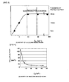
- Fig. 3 is a graph showing the relationship between the quantity of the silicone-based resin 40 placed in the oven 50 and the thickness of the siloxane film formed on the laminated substrate body 2. If the silicone-based resin 40 in the oven 50 is less than 10 g/m 3 , by changing the quantity of the silicone-based resin 40, the film thickness of the siloxane film can be adjusted. If the silicone-based resin 40 in the oven 50 is 10 g/m 3 or more, the film thickness becomes a constant value of about 20 nm. This is because the concentration of the siloxane in the oven 50 is saturated.
- Fig. 4 is a graph showing the relationship between the quantity of the silicone based resin 40 placed in the oven 50 and the wetted area of the laminated substrate body 2.
- the siloxane film is formed by means of a PVD process, the siloxane film is formed inside micro-level defects, thus, even migration or sulfuration originating from micro defects can also be suppressed.
- the thickness of the siloxane film is as thin as less than 100 nm, the levels of mountability of solder wettability and wire bondability of the lands 16 and 17 and the external electrodes 24 and 25, are accceptable.
- the surface of the siloxane film covering the laminated substrate body 2 is activated by cleaning by means of a process such as plasma (preferably oxygen plasma) irradiation or ultra-violet irradiation.
- a process such as plasma (preferably oxygen plasma) irradiation or ultra-violet irradiation.
- plasma preferably oxygen plasma
- ultra-violet irradiation a process such as oxygen plasma
- the external electrodes 13 and 14 of the mounting component 11 are electrically connected and firmly fixed to the lands 16 and 17 of the laminated substrate body 2 via solder 19.
- the resin sealing material 4 for sealing the mounting component 11 is formed on the laminated substrate body 2.
- a thermosetting resin such as an epoxy-based resin, or a photosensitive resin is desirable. Since the resin sealing material 4 has a good wettability with respect to the siloxane film, and the bonding strength between the silicone thin film and the laminated substrate body 2 is also high, the bonding strength between the resin sealing material 4 and the laminated substrate body 2 can be enhanced.
- soldering of the mounting component 11 may be performed either before or after the formation of the siloxane film.
- Table 2 is a table showing evaluated results of the ceramic multilayer substrate when soldering of the mounting component 11 is performed before and after the formation of the siloxane film.
- sample 1 is a ceramic multilayer substrate where, after the mounting component 11 is soldered to the laminated substrate body 2, the siloxane film is formed on the laminated substrate body 2, which is sealed with the resin sealing material 4.
- Sample 2 a ceramic multilayer substrate where, after the siloxane film is covered the laminated substrate body 2, the mounting component 11 is soldered to the laminated substrate body 2, which is sealed with the resin sealing material 4.
- sample 3 is a ceramic multilayer substrate where, without forming the siloxane film on the laminated substrate body 2, the mounting component 11 is soldered to the laminated substrate body 2, which is sealed with the resin sealing material 4.
- thermo cycle test was performed for 400 cycles at - 55°C/+125°C, and the state of peeling between the resin sealing material 4 and the laminated substrate body 2 was confirmed at the sides and at the cross section.
- the solder reflow test after moisture absorption was performed by standing samples for 40 hours under the conditions of 60°C and 60%RH, and subsequently, reflowing the samples at 260°C five times, and the state of peeling between the resin sealing material 4 and the laminated substrate body 2 was confirmed at the sides and at the cross section, and solder shortage was confirmed.
- the ceramic multilayer substrate 1A shown in Fig. 5 is substantially constituted by a laminated substrate body 2A, a mounting component 11 contained in a cavity 65 provided on the laminated substrate body 2A, and a resin sealing material 4A for sealing the mounting component 11.
- lands 16 and 17 are formed on the upper side of steps in the cavity 65 of the laminated substrate body 2A.
- the mounting component 11 is disposed in the cavity 65, and its external electrodes 13 and 14 are electrically connected to the lands 16 and 17 by wire bonding 61.
- internal electrode patterns 22 and 23 are formed in the inside of the laminated substrate body 2A.
- One end of the internal electrode pattern 22 and one end of the internal electrode pattern 23 are electrically connected to the lands 16 and 17, respectively, via via-hole conductors 20 formed in the laminated substrate body 2A.
- the other ends of the internal electrode patterns 22 and 23 are electrically connected to external electrodes 24 and 24, respectively.
- a Ni-Au plating film is formed on the lands 16 and 17 and on the external electrodes 24 and 25, a Ni-Au plating film is formed. Further, the entire laminated substrate body 2A including the lands 16 and 17 and the external electrodes 24 and 25 is covered with a siloxane film. The thickness of the siloxane film is set less than 100 nm. In Fig. 5, the siloxane film is not shown.
- a resin sealing material 4A for sealing the mounting component 11 is filled in the cavity 65 of the laminated substrate body 2A.
- a thermosetting resin such as an epoxy-based resin, or a photosensitive resin is desirable.
- the siloxane film covers the entire laminated substrate body 2A including the lands 16 and 17 and the external electrodes 24 and 25, the migration property is improved markedly. Meanwhile, since the thickness of the siloxane film is as thin as less than 100 nm, the levels of mountability of solder wettability and wire bondability of the lands 16 and 17 and the external electrodes 24 and 25 of the lands 16 and 17 and the external electrodes 24 and 25, are accceptable.
- the wire bonding may be performed either before or after the formation of the siloxane film.
- the resin sealing material 4A has a good wettability with respect to the siloxane film, and the bonding strength between the siloxane film and the laminated substrate body 2A is also high, the bonding strength between the resin sealing material 4 and the laminated substrate body 2A can be enhanced.
- the ceramic multilayer substrate 1B shown in Fig. 6, is constituted by a laminated substrate body 2, lands 16 formed on the upper surface of the laminated substrate body 2, and a siloxane film 70 provided so as to cover the laminated substrate body 2 and the lands 16.
- via-holes 20 for connecting between a conductive pattern 22 formed at an interface between layers and another conductive pattern 22 formed at another interface between layers, or the land 16, are formed.
- the laminated substrate body 2 is manufactured by the following manufacturing procedures. First, crystallized glass powder made of SiO 2 , Al 2 O 3 , B 2 O 3 , and CaO, and alumina powder are blended at an equal weight ratio. By adding polyvinyl-butyral of 15 parts by weight, isopropyl-alcohol of 40 parts by weight, and trole of 20 parts by weight to the blended powder of 100 parts by weight, and blending them in a ball mill for 24 hours, a slurry is made. By shaping the slurry to a sheet with a thickness of 120 ⁇ m by means of a doctor blade process, a ceramic green sheet is obtained.
- holes for via-holes are formed in predetermined ceramic green sheets. Subsequently, conductive paste is filled in the holes for via-holes to form via-hole conductors 20, and inner conductor patterns 22 are formed on eac.h ceramic green sheet by means of a screen printing process. Additionally, the via-hole conductors 20 may be formed by filling a conductive paste in holes for via-holes at the same time when the inner conductor patterns 22 are formed on each ceramic green sheet by means of the screen printing process.
- the ceramic green sheets After being stacked, the ceramic green sheets are contact bonded at a pressure of 50 MPa, and at a temperature of 60°C to form a laminated block. After the laminated block is cut into pieces having a predetermined size, the pieces are sintered in a lump. In this manner, they are made as low-temperature sintered ceramic laminated substrate bodies 2.
- lands 16 are formed.
- the lands 16 may be formed by forming a land pattern on a ceramic green sheet, and by sintering the land pattern and the ceramic green sheet, simultaneously.
- a plating film may be formed by subjecting the lands 16 to Ni-Au plating. In addition, the plating film may not be formed.
- a ceramic multilayer substrate 1B is produced by forming a siloxane film 70 with a thickness less than 100 nm on the laminated substrate body 2 so as to cover the laminated substrate body 2 and the lands 16.
- a siloxane film 70 with a thickness less than 100 nm on the laminated substrate body 2 so as to cover the laminated substrate body 2 and the lands 16.
- the whole surface of the laminated substrate body 2 is covered with the siloxane film, at least the principal surface on which the lands 16 are formed, should be covered, for example, the bottom surface may not be covered.
- the siloxane film 70 covers the entire laminated substrate body 2 including the lands 16, the migration resistance can be improved markedly, and environmental characteristics such as sulfuration and oxidization are also improved. Meanwhile, since the thickness of the siloxane film 70 is as thin as less than 100 nm, the levels of mountability of solder wettability and wire bondability of the lands 16, are acceptable.
- the ceramic multilayer substrate 1C shown in Fig. 7 is substantially constituted by a laminated substrate body 2, mounting components 11 mounted on the laminated substrate body 2, and a siloxane film 70 provided so as to cover the laminated substrate body 2 and the mounting components 11.
- lands 16 are formed on the upper surface of the laminated substrate body 2.
- the siloxane film 70 is not formed, however, the siloxane film 70 may be formed on these parts.
- the ceramic multilayer substrate 1C is manufactured by the following procedures.
- the laminated substrate body 2 is formed by means of a method similar to that of the above-mentioned second embodiment.
- a siloxane film 70 with a thickness less than 100 nm is formed.
- the mounting components 11 are mounted on the lands 16 on which the siloxane film 70 is formed, via the solder 19.
- the siloxane film 70 is formed again so as to cover the mounting components 11 and at a least part of such a part of the solder 19 that is not contacted to the lands 16 and the external electrodes 13, and exposed.
- the siloxane film 70 may be formed further on the laminated substrate body 2.
- the siloxane film 70 covers the entire laminated substrate body 2 including the lands 16, the migration resistance can be improved markedly, and environmental characteristics such as sulfuration and oxidization are also improved. Moreover, since the mounting components 11 are also covered with the siloxane film 70, chemical envioronmental characteristics such as sulfuration or oxidation of the mounting components 11 is also improved. Meanwhile, since the thickness of the siloxane film 70 is as thin as less than 100 nm, the levels of mountability of solder wettability and wire bondability of the lands 16, are acceptable.
- the siloxane film 70 covers at least a part of the solder 19, in a reflow step when the ceramic multilayer substrate 1C is mounted on the other substrate, flushing out of the solder 19 is suppressed.
- FOURTH EMBODIMENT see Fig. 8
- the ceramic multilayer substrate 1D shown in Fig. 8 is substantially constituted by a laminated substrate body 2, mounting components 11 mounted on the laminated substrate body 2, and a siloxane film 70 provided so as to cover the laminated substrate body 2 and the mounting components 11.
- lands 16 are formed on the upper surface of the laminated substrate body 2.
- at least a part of such a part of the solder 19 that is not contacted to the lands 16 and the external electrodes 13, and exposed, is covered with the siloxane film 70.
- via-holes 20 for connecting between a conductive pattern 22 formed at an interface between layers and another conductive pattern 22 formed at another interface between layers, or the land 16, are formed.
- the siloxane film 70 is not formed, however, the siloxane film 70 may be formed on these parts.
- the ceramic multilayer substrate 1D is manufactured by the following procedures.
- the laminated substrate body 2 is formed by means of a method similar to that of the above-mentioned second embodiment.
- the mounting components 11 are mounted on the lands 16 via the solder 19.
- the siloxane film 70 is formed again so as to cover the mounting components 11 and at a least part of such a part of the solder 19 that is not contacted to the lands 16 and the external electrodes 13, and exposed.
- the siloxane film 70 covers the laminated substrate body 2 mounting components 11, ant at least a part of the lands 16, the migration resistance can be improved markedly, and environmental characteristics such as sulfuration and oxidization are also improved. Moreover, since the mounting components 11 are also covered with the siloxane film 70, chemical envioronmental characteristics such as sulfuration or oxidation of the mounting components 11 is also improved. Moreover, since the siloxane film 70 covers at least a part of the solder 19, in a reflow step when the ceramic multilayer substrate 1D is mounted on the other substrate, flushing out of the solder 19 is suppressed.
- the ceramic multilayer substrate IE shown in Fig. 9 is constituted by a laminated substrate body 1B (see the second embodiment and Fig. 6), mounting components 11 mounted on the laminated substrate body 1B, a resin sealing material 4 for sealing the mounting components, and a siloxane film 70 provided so as to cover the resin sealing material 4.
- lands 16 covered with the siloxane film 70 are formed on the upper surface of the ceramic multilayer substrate 1B.
- the ceramic multilayer substrate 1E is manufactured by the following procedures.
- the surface of the siloxane film 70 covering the ceramic multilayer substrate 1B produced by means of a method similar to that of the above-mentioned second embodiment is activated by cleaning by means of a process such as plasma (preferably, oxygen plasma) irradiation or ultraviolet irradiation.
- a process such as plasma (preferably, oxygen plasma) irradiation or ultraviolet irradiation.
- the mounting components 11 are mounted via the solder 19.
- a resin sealing material 4 for sealing the mounting components 11 is formed.
- the material of the resin sealing material 4 a material similar to that described in the first embodiment can be used.
- the siloxane film 70 is formed so as to cover the resin sealing material 4.
- the siloxane film 70 may be formed further on the laminated substrate body 2.
- the siloxane film 70 is formed on the resin sealing material 4, rather, the siloxane film 70 may not be formed so as to cover the resin sealing material 4.
- ceramic multilayer substrates 1F and 1G shown in Figs. 10 and 11, they respectively include the ceramic multilayer substrate 1C (see the third embodiment and Fig. 7) and the resin sealing material 4 on which a siloxane film 70 is formed, and the ceramic multilayer substrate 1D (see the fourth embodiment and Fig. 8) and the resin sealing material 4 on which a siloxane film 70 is formed.
- the methods for forming the resin sealing material 4 and the siloxane film 70 are similar to those of in the first embodiment. Although, in Figs. 10 and 11, the siloxane film 70 is formed on the resin sealing material 4, rather, the siloxane film 70 may not be formed so as to cover the resin sealing material 4.
- the siloxane film 70 is formed on the interface between the resin sealing material 4 and the laminated substrate body 2, the bonding strength between the resin sealing material 4 and the laminated substrate body 2 can be enhanced.
- the resin sealing material 4 is covered with the siloxane film 70, the moisture absorption of the resin sealing material 4 can be suppressed, thereby, enabling to suppress the change of the characteristics of the mounting components 11 due to the moisture absorbed by the resin sealing material 4, or impurities occurred by hydrolytic cleavage of the resin sealing material 4.
- the siloxane film 70 covers the sides of the interface between the resin sealing material 4 and the laminated substrate body 2, peeling of the interface between the laminated substrate body 2 and the resin sealing material 4 can be suppressed more surely.
- the ceramic multilayer substrate 1H shown in Fig. 12 is constituted by a laminated substrate body 2, mounting components 11 mounted on the laminated substrate body 2, a resin sealing material 4 for sealing the mounting components 11, and a siloxane film 70 provided so as to cover the laminated substrate body 2 and the resin sealing material 4.
- lands 16 are formed on the upper surface of the laminated substrate body 2.
- the ceramic multilayer substrate 1H is manufactured by the following procedures. On the lands 16 of the ceramic multilayer substrate 2 produced by means of a method similar to that of the second embodiment, the mounting components 11 are mounted via the solder 19. Next, the resin sealing material 4 for sealing the mounting components 11 is formed. As for the material of the resin sealing material 4, a material similar to that described in the first embodiment can be used. After that, by means of a method similar to that of the first embodiment, the siloxane film is formed so as to cover the laminated substrate body 2 and the resin sealing material 4.
- the siloxane film 70 is covered with the siloxane film 70, the moisture absorption of the resin sealing material 4 can be suppressed, thereby, enabling to suppress the change of the characteristics of the mounting components 11 due to the moisture absorbed by the resin sealing material 4, or impurities occurred by hydrolytic cleavage of the resin sealing material 4. Further, since the siloxane film 70 covers the sides of the interface between the resin sealing material 4 and the laminated substrate body 2, peeling of the interface between the laminated substrate body 2 and the resin sealing material 4 can be suppressed more surely.
- the ceramic multilayer substrate 1I shown in Fig. 13(a) is constituted by a laminated substrate body 2, lands 16 formed on the upper side of the laminated substrate body 2, a mounting component 11 mounted on the lands 16 via solder 19, and a siloxane film 70 provided so as to cover the laminated substrate body 2 the mounting component 11 and at least a part of the solder 19.
- via-holes 20 for connecting between a conductive pattern 22 formed at an interface between layers and another conductive pattern 22 formed at another interface between layers, or the land 16 are formed.
- the ceramic multilayer substrate 1I is manufactured by the following procedures. As shown in Fig. 13(b), first, by means of a method similar to that of the above-mentioned second embodiment, a ceramic multilayer substrate 1B, in which the laminated substrate body 2 and lands 1,6 formed on the upper surface of the laminated substrate body 2 are covered with the siloxane film 70, is produced. Meanwhile, solder balls 19A are formed on the external electrodes 13 of the mounting component 11, after that, the siloxane film 70 is formed so as to cover the mounting component 11 and the solder balls 19A.
- the siloxane film 70 is formed by means of a method similar to that of the above-mentioned first embodiment.
- the mounting component 11 is connected to the upper surface of the ceramic multilayer substrate 1B, thereby resulting in the production of the ceramic multilayer substrate 1l.
- the migration resistance can be improved markedly, thereby, chemical environmental characteristics such as sulfuration or the oxidation is also improved.
- the mounting component 11 is also covered with the siloxane film 70, chemical environmental characteristics such as sulfuration or the oxidation of the mounting component 11, is also improved.
- the ceramic multilayer substrate 1J shown in Fig. 14(a) is constituted by a laminated substrate body 2, lands 16 formed on the upper side of the laminated substrate body 2, a mounting component 11 mounted on the lands 16 via solder 19, and a siloxane film 70 provided so as to cover the laminated substrate body 2 the mounting component 11 and at least a part of the solder 19.
- via-holes 20 for connecting between a conductive pattern 22 formed at an interface between layers and another conductive pattern 22 formed at another interface between layers, or the land 16 are formed.
- the ceramic multilayer substrate 1J is manufactured by the following procedures. As shown in Fig. 14(b), first, solder balls 19A are formed on the lands 16 formed on the upper surface of the laminated substrate body 2. Next, the siloxane film 70 is formed so as to cover the laminated substrate body 2 and the solder balls 19A. Meanwhile, the siloxane film 70 is formed so as to cover the mounting component 11 and its external electrodes 13. The siloxane film 70 is formed by means of a method similar to that of the first embodiment.
- the mounting component 11 is connected to the upper surface of the laminated substrate body 2, thereby, resulting in the production of the ceramic multilayer substrate 1J.
- the siloxane film 70 covers the sides of the lands 16 that are not contacted to the solder 19 and the entire laminated substrate body 2, the migration resistance can be improved markedly, thereby, chemical environmental characteristics such as sulfuration or the oxidation is also improved. Moreover, since the mounting component 11 is also covered with the siloxane film 70, thereby, chemical environmental characteristics such as sulfuration or the oxidation of the mounting component 11 is also improved.
- the ceramic multilayer substrate 1K shown in Fig. 15, is constituted by a laminated substrate body 1I (see the seventh embodiment and Fig. 13) or a laminated substrate body 1J (see the eighth embodiment and Fig. 14), a resin sealing material 4 for sealing the mounting component 11 on the ceramic multilayer substrate 1I or 1J, and a siloxane film 70 provided so as to cover the resin sealing material 4.
- the ceramic multilayer substrate 1K is manufactured by the following procedures.
- the surface of the siloxane film 70 covering the ceramic multilayer substrate 1I or 1J produced by means of a method similar to that of the above-mentioned seventh and eighth embodiments, is activated by cleaning by means of a process such as plasma (preferably, oxygen plasma) irradiation or ultraviolet irradiation.
- the resin sealing material 4 for sealing the mounting component 11 is formed on the ceramic multilayer substrate 1I or 1J.
- the material of the resin sealing material 4 a material similar to that described in the first embodiment can be used.
- the siloxane film 70 is formed so as to cover the resin sealing material 4.
- the siloxane film 70 may be formed further on the laminated substrate body 2.
- the siloxane film 70 may not be formed so as to cover the resin sealing material 4.
- the siloxane film 70 is formed at the interface between the resin sealing material 4 and the laminated substrate body 2, the bonding strength between the resin sealing material 4 and the laminated substrate body 2 can be enhanced.
- the resin sealing material 4 is covered with the siloxane film 70, the moisture absorption of the resin sealing material 4 can be suppressed, thereby, enabling to suppress the change of the characteristics of the mounting component 11 due to the moisture absorbed by the resin sealing material 4, or impurities occurred by hydrolytic cleavage of the resin sealing material 4.
- the siloxane film 70 covers the sides of the interface between the resin sealing material 4 and the laminated substrate body 2, peeling of the interface between the laminated substrate body 2 and the resin sealing material 4 can be suppressed more surely.
- ceramic multilayer substrates according to the present invention and its manufacturing methods are not intended to be limited to the above-mentioned embodiments, rather, they can be changed variously within the scope of the present invention.
- the laminated substrate body is formed by stacking ceramic green sheets, were shown, however, an embodiment where the laminated substrate body is formed by means of a method of alternately recoating ceramic paste and conductive paste, may be possible.
- the present invention is useful for a ceramic multilayer substrate for mounting an electronic component such as IC component on the surface thereof, and its manufacturing method, especially, it is excellent in that the migration resistance is good, and the bonding strength between a resin sealing material and a ceramic multilayer substrate body becomes higher.
Landscapes
- Engineering & Computer Science (AREA)
- Manufacturing & Machinery (AREA)
- Microelectronics & Electronic Packaging (AREA)
- Non-Metallic Protective Coatings For Printed Circuits (AREA)
- Production Of Multi-Layered Print Wiring Board (AREA)
- Structures Or Materials For Encapsulating Or Coating Semiconductor Devices Or Solid State Devices (AREA)
Abstract
Description
- The present invention relates to a ceramic multilayer substrate, especially, to a ceramic multilayer substrate for mounting an electronic component such as an IC component on its surface, and its manufacturing method.
- In general, in a ceramic multilayer substrate, Ag- or Cu- based lands for mounting a mounting component and further external electrodes for mounting the multilayer substrate itself are formed on the substrate surface. On the lands and the external electrodes, a solderable and wire-bondable plating film is formed. The plating film also has an effect of suppressing the migration of the lands and the external electrodes.
- However, previously, when a ceramic multilayer substrate was used under a high electric field, since the plating film formed on the lands and the external electrodes did not sufficiently suppress the migration, the formation of a protective film made of glass or resin in addition to the plating film has been required. Consequently, there have been problems related to design constraints and the increase in the manufacturing cost, due to the formation of the protective film.
- Moreover, as described in
Patent Document 1, in order to protect the mounting component mounted on the ceramic multilayer substrate, in some cases, the mounting component is sealed with a resin sealing material. However, since the wettability between the resin sealing material and the ceramic multilayer substrate body is not good, there has also been a problem that the bonding strength between the resin sealing material and the ceramic multilayer substrate body is not sufficient. - In addition, as for the technologies for forming a siloxane film by means of sputtering, they are described in
Patent Document 2 and Patent Document 3. - Patent Document 1:
Japanese Unexamined Patent Application Publication No. 2003-249840 - Patent Document 2:
Japanese Unexamined Patent Application Publication No. 06-152109 - Patent Document 3:
Japanese Unexamined Patent Application Publication No. 08-213742 - Consequently, the object of the present invention is to provide a ceramic multilayer substrate that has excellent migration resistance and high bonding strength between the resin sealing material and the ceramic multilayer substrate body, and its manufacturing method.
- In order to achieve the above-mentioned object, the ceramic multilayer substrate according to a first invention characterized in including a laminated substrate body constituted by stacking a plurality of ceramic layers and inner conductor layers, lands provided on the surface of the laminated substrate body for being electrically connected to the external electrodes of the mounting component; and a siloxane film provided so as to cover the laminated substrate body and the land, and having a thickness less than 100 nm.
- As for the ceramic multilayer substrate according to the first invention, further, it is preferable for the siloxane film to be provided so as to cover the mounting component mounted on the lands via solder and at least a par of the solder.
- The ceramic multilayer substrate according to a second invention characterized in including a laminated substrate body constituted by stacking a plurality of ceramic layers and inner conductor layers; lands provided on the surface of the laminated substrate body for being electrically connected to the external electrodes of the mounting component; a mounting component mounted on the lands via solder; and a siloxane film provided so as to cover the laminated substrate body, the mounting component, and at least a part of the solder, and having a thickness less than 100 nm.
- As for the ceramic multilayer substrates according to the first and second inventions, further they are preferable to include a resin sealing material for sealing the mounting component. Further, it is preferable for the resin sealing material to be covered with a siloxane film.
- The ceramic multilayer substrate according to a third invention characterized in including a laminated substrate body constituted by stacking a plurality of ceramic layers and inner conductor layers; lands provided on the surface of the laminated substrate body for being electrically connected to the external electrodes of the mounting component; the mounting component mounted on the lands via solder; a resin sealing material for sealing the mounting component; and a siloxane film provided so as to cover the laminated substrate body and the resin sealing material, and having a thickness less than 100 nm.
- In the ceramic multilayer substrates according to the first to third inventions, it is preferable for the mounting component to include an IC component and to be electrically connected to the lands by means of wire bonding. The IC component may be contained in a cavity provided on one principal surface of the laminated substrate body. Moreover, a plating film may also be formed on the lands.
- The manufacturing method of a ceramic multilayer substrate according to a fourth invention characterized in including steps of constituting a laminated substrate body by stacking a plurality of ceramic layers and inner conductor layers; forming lands on the surface of the laminated substrate body to be electrically connected to the external electrodes of a mounting component; and forming a siloxane film with a thickness less than 100 nm so as to cover the laminated substrate body and the lands by means of a PVD process.
- As for the manufacturing method of a ceramic multilayer substrate according to the fourth invention, further they may include steps of mounting a mounting component on the lands on which the siloxane film is formed, via solder; and forming a siloxane film with a thickness less than 100 nm so as to cover the mounting component and at least a part of the solder by means of a PVD process.
- The manufacturing method of a ceramic multilayer substrate according to a fifth invention characterized in including steps of constituting a laminated substrate body by stacking a plurality of ceramic layers and inner conductor layers; forming lands to be electrically connected to the external electrodes of a mounting component on the surface of the laminated substrate body; mounting the mounting component on the lands via solder; and forming a siloxane film with a thickness less than 100 nm so as to cover the mounting component and at least a part of the solder by means of a PVD process.
- As for the manufacturing methods of a ceramic multilayer substrate according to the fourth and fifth inventions, they may include a step of sealing the mounting component with a resin sealing material subsequent to the step of forming the siloxane film so as to cover the mounting component by means of the PVD process. Further they may include a step of forming a siloxane film with a thickness less than 100 nm so as to cover the resin sealing
material 1 by means of the PVD process. - The manufacturing method of a ceramic multilayer substrate according to a sixth invention characterized in including steps of constituting a laminated substrate body by stacking a plurality of ceramic layers and inner conductor layers; forming lands to be electrically connected to the external electrodes of a mounting component on the surface of the laminated substrate body; mounting the mounting component, on the lands via solder; sealing the mounting component with a resin sealing material; and forming a siloxane film with a thickness less than 100 nm so as to cover the laminated substrate body and the resin sealing material by means of a PVD process.
- The manufacturing method of a ceramic multilayer substrate according to a seventh invention characterized in including steps of constituting a laminated substrate body by stacking a plurality of ceramic layers and inner conductor layers; forming lands to be electrically connected to the external electrodes of a mounting component, on the surface of the laminated substrate body; forming solder balls on the lands; forming a siloxane film with a thickness below 100 nm so as to cover the lands and the solder balls by means of a PVD process; forming a siloxane film with a thickness less than 100 nm so as to cover the mounting component by means of a PVD process; and mounting the mounting component on the lands via solder balls.
- The manufacturing method of a ceramic multilayer substrate according to an eighth invention characterized in including steps of constituting a laminated substrate body by superposing a plurality of ceramic layers and inner conductor layers; forming lands to be electrically connected to the external electrodes of a mounting component, on the surface of the laminated substrate body; forming solder balls on the lands; forming a siloxane film with a thickness less than 100 nm so as to cover the laminated substrate body and the lands by means of a PVD process; forming solder balls on the mounting component; forming a siloxane film with a thickness less than 100 nm so as to cover the mounting component and the solder balls by means of a PVD process; and mounting the mounting component on the lands via solder balls.
- As for the manufacturing methods of a ceramic multilayer substrate according to the seventh and eighth inventions, they may include a step of sealing the mounting component with a resin sealing material subsequent to the step of mounting the mounting component. Further they may include a step of forming a siloxane film with a thickness less than 100 nm so as to cover the laminated substrate body and the resin sealing material by means of the PVD process.
- As for the manufacturing methods of a ceramic multilayer substrate according to the fourth to eighth inventions, they preferably include a step of activating the surface of the siloxane film. The step of activating the siloxane film preferably performed by subjecting the surface of the siloxane film to cleaning using oxygen plasma. Advantages of the Invention
- According to the present invention, since a siloxane film with a thickness less than 100 nm is provided so as to cover a laminated substrate body and lands, by a water repellent effect, the migration resistance can be improved, and chemical environmental characteristics such as sulfuration and oxidation, is also improved. Further, since the thickness of the siloxane film is less than 100 nm, soldering and wire bonding can be performed without problems.
- If both of the laminated substrate body and the mounting component mounted via solder are covered with a siloxane film, the siloxane film covers the exposed portion of the solder, thereby, enabling to suppress flushing out of the solder.
- Moreover, when a resin sealing material for sealing the mounting component is included, the wettability between the resin sealing material and the siloxane film is good, and the bonding strength between the siloxane film and the laminated substrate body is also high, thereby, enabling to enhance the bonding strength between the resin sealing material and the laminated substrate body.
- If the resin sealing material is provided so as to cover the siloxane film, the moisture absorption of the resin sealing material is suppressed, thereby, enabling to suppress the change of the characteristics of the mounting component due to the moisture absorbed by the resin sealing material, or impurities occurred by hydrolysis of the resin sealing material.
- Moreover, if the laminated substrate body and the resin sealing material are simultaneously covered with a siloxane film, the sides of the interface between the laminated substrate body and the resin sealing material are covered with the siloxane film, thereby, enabling to suppress peeling of the interface between the laminated substrate body and the resin sealing material.
- If a mounting component is mounted on the substrate body via solder balls covered with the siloxane film, the flushing out of the solder can be further surely suppressed.
-
- [Fig. 1] Fig. 1 is a sectional view showing a first embodiment of a ceramic multilayer substrate according to the present invention.
- [Fig. 2] Fig. 2 is an illustrative view showing the step of forming a siloxane film.
- [Fig. 3] Fig. 3 is a graph showing the relationship between the quantity of silicone based resin and the thickness of the siloxane film.
- [Fig. 4] Fig. 4 is a graph showing the relationship between the quantity of silicone based resin and the area of wetting.
- [Fig. 5] Fig. 5 is a sectional view showing a modified embodiment of a first embodiment of a ceramic multilayer substrate according to the present invention.
- [Fig. 6] Fig. 6 is a sectional view showing a second embodiment of a ceramic multilayer substrate according to the present invention.
- [Fig. 7] Fig. 7 is a sectional view showing a third embodiment of a ceramic multilayer substrate according to the present invention.
- [Fig. 8] Fig. 8 is a sectional view showing a fourth embodiment of a ceramic multilayer substrate according to the present invention.
- [Fig. 9] Fig. 9 is a sectional view showing a fifth embodiment of a ceramic multilayer substrate according to the present invention.
- [Fig. 10] Fig. 10 is a sectional view showing a modified embodiment of a fifth embodiment of a ceramic multilayer substrate according to the present invention.
- [Fig. 11] Fig. 11 is a sectional view showing another modified embodiment of the fifth embodiment 5 of a ceramic multilayer substrate according to the present invention.
- [Fig. 12] Fig. 12 is a sectional view showing a sixth embodiment 6 of a ceramic multilayer substrate according to the present invention.
- [Fig. 13] Fig. 13 is a sectional view showing a seventh embodiment 7 of a ceramic multilayer substrate according to the present invention.
- [Fig. 14] Fig. 14 is a sectional view showing an eighth embodiment of a ceramic multilayer substrate according to the present invention.
- [Fig. 15] Fig. 15 is a sectional view showing a ninth embodiment of a ceramic multilayer substrate according to the present invention.
- Hereinafter, referring to the appended drawings, embodiments of a ceramic multilayer substrate and its manufacturing method according to the present invention will be described.
- The
ceramic multilayer substrate 1 shown in Fig. 1, is substantially constituted by a laminatedsubstrate body 2, a mounting component (IC component) 11 mounted on the laminatedsubstrate body 2, and a resin sealing material 4 for sealing themounting component 11. -
Lands laminated substrate body 2. The mountingcomponent 11, whoseexternal electrodes lands solder 19, is mounted on thelaminated substrate body 2. - In the inside of the
laminated substrate body 2,inner conductor patterns inner conductor pattern 22 and one end of theinner conductor pattern 23 are electrically connected tolands hole conductors 20 formed in thelaminated substrate body 2. The other ends of theinner conductor patterns external electrodes laminated substrate body 2. - The
laminated substrate body 2 is manufactured by the following manufacturing procedures. First, crystallized glass powder made of SiO2, Al2O3, B2O3, and CaO, and alumina powder are blended at an equal weight ratio. By adding polyvinyl-butyral of 15 parts by weight, isopropyl-alcohol of 40 parts by weight, and trole of 20 parts by weight to the blended powder of 100 parts by weight, and blending them in a ball mill for 24 hours, a slurry is made. By shaping the slurry to a sheet with a thickness of 120 µm by means of a doctor blade process, a ceramic green sheet is obtained. - Next, holes for via-holes are formed in predetermined ceramic green sheets. Subsequently, conductive paste is filled in the holes for via-holes to form via-
hole conductors 20, andinner conductor patterns hole conductors 20 may be formed by filling a conductive paste in holes for via-holes at the same time when theinner conductor patterns - After being stacked, the ceramic green sheets are contact bonded at a pressure of 50 MPa, and at a temperature of 60°C to form a laminated block. After the laminated block is cut into pieces having a predetermined size, the pieces are sintered in a lump. In this manner, they are made as low-temperature sintered ceramic
laminated substrate bodies 2. - Next, by coating conductive paste on the surface of the
laminated substrate body 2, and subsequent baking thereof, lands 16 and 17, andexternal electrodes lands external electrodes - Next, as shown in Fig. 2, silicone based
resin 40 contained in acrucible 51 and thelaminated substrate body 2 are placed together in anoven 50 to be sealed, and heated by aheater 52. At this time,siloxane 42 that is a constituent of the silicone basedresin 40 is vaporized to be deposited on the surface of thelaminated substrate body 2. In this manner, the entirelaminated substrate body 2 including thelands external electrodes - As the siloxane film is formed by means of a PVD process, rather than a CVD (Chemical Vapor Deposition) process or a plasma process, since only heating the siloxane film together with the silicone-based
resin 40 is required, the siloxane film can be formed easily and at a low price. - The curing conditions for the silicone based
resin 40 are, for example, 150°C for 2 hours. When the silicone-basedresin 40 is cured, itsconstituent siloxane 42 is vaporized, the concentration of the siloxane in theoven 50 becomes highest at 150°C, and together with the vaporization, deposition on the surface of thelaminated substrate body 2 also occurs. After the silicone-basedresin 40 is cured, when the temperature within theoven 50 is lowered, thesiloxane 42 is further deposited on the surface of thelaminated substrate body 2, as its saturated vaporization pressure becomes smaller. - Fig. 3 is a graph showing the relationship between the quantity of the silicone-based
resin 40 placed in theoven 50 and the thickness of the siloxane film formed on thelaminated substrate body 2. If the silicone-basedresin 40 in theoven 50 is less than 10 g/m3, by changing the quantity of the silicone-basedresin 40, the film thickness of the siloxane film can be adjusted. If the silicone-basedresin 40 in theoven 50 is 10 g/m3 or more, the film thickness becomes a constant value of about 20 nm. This is because the concentration of the siloxane in theoven 50 is saturated. - Items as shown in Table 1 were evaluated with respect to a
laminated substrate body 2 thus produced. For comparison, a laminated substrate body on which a siloxane film was not formed, was also evaluated. The occurrence of migration was evaluated under testing conditions of 85°C, 85% RH, and 50VDC. Sulfuration was evaluated by standing thesubstrate bodies 2 in an atmosphere of hydrogen sulfide for one minute. Solder wettability was determined as acceptable when 95% or more of a square land of 2 mm x 2 mm dipped with Sn-Pb solder was wet with solder. Wire bondability was determined as acceptable when a square land of 2 mm x 2 mm bonded to a wire and had a bonding strength of 2 gf or more.Table 1 Siloxane PVD protective film present not present Occurrence of migration none occurred Evaluation of sulfuration acceptable silver sulfide precipitated on the edge part Solder wettability acceptable acceptable Wire bondability min:3.9 gf min:4.0 gf - As is clear from Table 1, since the siloxane film covers the entire
laminated substrate body 2 includinglands external electrodes resin 40 placed in theoven 50 and the wetted area of thelaminated substrate body 2. - Further, environmental characteristics such as sulfuration and oxidization are also improved. Since the siloxane film is formed by means of a PVD process, the siloxane film is formed inside micro-level defects, thus, even migration or sulfuration originating from micro defects can also be suppressed.
- Meanwhile, since the thickness of the siloxane film is as thin as less than 100 nm, the levels of mountability of solder wettability and wire bondability of the
lands external electrodes - Next, the surface of the siloxane film covering the
laminated substrate body 2 is activated by cleaning by means of a process such as plasma (preferably oxygen plasma) irradiation or ultra-violet irradiation. This enables further improvement in the wettability with respect to the resin sealing material 4. After that, theexternal electrodes component 11 are electrically connected and firmly fixed to thelands laminated substrate body 2 viasolder 19. - Next, the resin sealing material 4 for sealing the mounting
component 11 is formed on thelaminated substrate body 2. As for the material of the resin sealing material 4, a thermosetting resin such as an epoxy-based resin, or a photosensitive resin is desirable. Since the resin sealing material 4 has a good wettability with respect to the siloxane film, and the bonding strength between the silicone thin film and thelaminated substrate body 2 is also high, the bonding strength between the resin sealing material 4 and thelaminated substrate body 2 can be enhanced. - In addition, soldering of the mounting
component 11 may be performed either before or after the formation of the siloxane film. Table 2 is a table showing evaluated results of the ceramic multilayer substrate when soldering of the mountingcomponent 11 is performed before and after the formation of the siloxane film. - In other words,
sample 1 is a ceramic multilayer substrate where, after the mountingcomponent 11 is soldered to thelaminated substrate body 2, the siloxane film is formed on thelaminated substrate body 2, which is sealed with the resin sealing material 4. Sample 2 a ceramic multilayer substrate where, after the siloxane film is covered thelaminated substrate body 2, the mountingcomponent 11 is soldered to thelaminated substrate body 2, which is sealed with the resin sealing material 4. For comparison, sample 3 is a ceramic multilayer substrate where, without forming the siloxane film on thelaminated substrate body 2, the mountingcomponent 11 is soldered to thelaminated substrate body 2, which is sealed with the resin sealing material 4.
- The thermo cycle test was performed for 400 cycles at - 55°C/+125°C, and the state of peeling between the resin sealing material 4 and the
laminated substrate body 2 was confirmed at the sides and at the cross section. The solder reflow test after moisture absorption was performed by standing samples for 40 hours under the conditions of 60°C and 60%RH, and subsequently, reflowing the samples at 260°C five times, and the state of peeling between the resin sealing material 4 and thelaminated substrate body 2 was confirmed at the sides and at the cross section, and solder shortage was confirmed. - Moreover, the ceramic multilayer substrate 1A shown in Fig. 5, is substantially constituted by a
laminated substrate body 2A, a mountingcomponent 11 contained in acavity 65 provided on thelaminated substrate body 2A, and aresin sealing material 4A for sealing the mountingcomponent 11. - On the upper side of steps in the
cavity 65 of thelaminated substrate body 2A, lands 16 and 17 are formed. The mountingcomponent 11 is disposed in thecavity 65, and itsexternal electrodes lands wire bonding 61. - In the inside of the
laminated substrate body 2A,internal electrode patterns internal electrode pattern 22 and one end of theinternal electrode pattern 23 are electrically connected to thelands hole conductors 20 formed in thelaminated substrate body 2A. The other ends of theinternal electrode patterns external electrodes - On the
lands external electrodes laminated substrate body 2A including thelands external electrodes - Further, a
resin sealing material 4A for sealing the mountingcomponent 11 is filled in thecavity 65 of thelaminated substrate body 2A. As for the material of theresin sealing material 4A, a thermosetting resin such as an epoxy-based resin, or a photosensitive resin is desirable. - In the ceramic multilayer substrate 1A composed of the above-mentioned configuration, since the siloxane film covers the entire
laminated substrate body 2A including thelands external electrodes lands external electrodes lands external electrodes resin sealing material 4A has a good wettability with respect to the siloxane film, and the bonding strength between the siloxane film and thelaminated substrate body 2A is also high, the bonding strength between the resin sealing material 4 and thelaminated substrate body 2A can be enhanced. - Next, a second embodiment of a ceramic multilayer substrate according to the present invention and its manufacturing method will be described. The
ceramic multilayer substrate 1B shown in Fig. 6, is constituted by alaminated substrate body 2, lands 16 formed on the upper surface of thelaminated substrate body 2, and asiloxane film 70 provided so as to cover thelaminated substrate body 2 and thelands 16. In the inside of thelaminated substrate body 2, via-holes 20 for connecting between aconductive pattern 22 formed at an interface between layers and anotherconductive pattern 22 formed at another interface between layers, or theland 16, are formed. - The
laminated substrate body 2 is manufactured by the following manufacturing procedures. First, crystallized glass powder made of SiO2, Al2O3, B2O3, and CaO, and alumina powder are blended at an equal weight ratio. By adding polyvinyl-butyral of 15 parts by weight, isopropyl-alcohol of 40 parts by weight, and trole of 20 parts by weight to the blended powder of 100 parts by weight, and blending them in a ball mill for 24 hours, a slurry is made. By shaping the slurry to a sheet with a thickness of 120 µm by means of a doctor blade process, a ceramic green sheet is obtained. - Next, holes for via-holes are formed in predetermined ceramic green sheets. Subsequently, conductive paste is filled in the holes for via-holes to form via-
hole conductors 20, andinner conductor patterns 22 are formed on eac.h ceramic green sheet by means of a screen printing process. Additionally, the via-hole conductors 20 may be formed by filling a conductive paste in holes for via-holes at the same time when theinner conductor patterns 22 are formed on each ceramic green sheet by means of the screen printing process. - After being stacked, the ceramic green sheets are contact bonded at a pressure of 50 MPa, and at a temperature of 60°C to form a laminated block. After the laminated block is cut into pieces having a predetermined size, the pieces are sintered in a lump. In this manner, they are made as low-temperature sintered ceramic
laminated substrate bodies 2. - Next, by coating conductive paste on the surface of the
laminated substrate body 2, and subsequent baking thereof, lands 16 are formed. In addition, thelands 16 may be formed by forming a land pattern on a ceramic green sheet, and by sintering the land pattern and the ceramic green sheet, simultaneously. Further, a plating film may be formed by subjecting thelands 16 to Ni-Au plating. In addition, the plating film may not be formed. - Next, by means of a method similar to that of the above-mentioned first embodiment, a
ceramic multilayer substrate 1B is produced by forming asiloxane film 70 with a thickness less than 100 nm on thelaminated substrate body 2 so as to cover thelaminated substrate body 2 and thelands 16. In addition, in Fig. 6, although the whole surface of thelaminated substrate body 2 is covered with the siloxane film, at least the principal surface on which thelands 16 are formed, should be covered, for example, the bottom surface may not be covered. - In the
ceramic multilayer substrate 1B composed of the above-mentioned configuration, since thesiloxane film 70 covers the entirelaminated substrate body 2 including thelands 16, the migration resistance can be improved markedly, and environmental characteristics such as sulfuration and oxidization are also improved. Meanwhile, since the thickness of thesiloxane film 70 is as thin as less than 100 nm, the levels of mountability of solder wettability and wire bondability of thelands 16, are acceptable. - Next, a third embodiment of a ceramic multilayer substrate according to the present invention and its manufacturing method will be described. The
ceramic multilayer substrate 1C shown in Fig. 7, is substantially constituted by alaminated substrate body 2, mountingcomponents 11 mounted on thelaminated substrate body 2, and asiloxane film 70 provided so as to cover thelaminated substrate body 2 and the mountingcomponents 11. - On the upper surface of the
laminated substrate body 2, lands 16 are formed. The mountingcomponent 11, whose external electrodes provided on its bottom surface are bonded to thelands 16 viasolder 19, is mounted on thelaminated substrate body 2. At least a part of such a part of thelands 16 that is not contacted to thesolder 19 and exposed, is covered with thesiloxane film 70. At least a part of the part of thesolder 19 which is exposed and not contacted to thelands 16 and theexternal electrodes 13, is covered with thesiloxane film 70. In the inside of thelaminated substrate body 2, via-holes 20 for connecting between aconductive pattern 22 formed at an interface between layers and anotherconductive pattern 22 formed at another interface between layers, or theland 16, are formed. In addition, in Fig. 7, as for the mountingcomponent 11, whoseexternal electrodes 13 are formed on its bottom surface, of the mountingcomponents 11, on the sides of theexternal electrodes 13 formed on the center of the mountingcomponent 11 and on the sides of thesolder 19 connected to theexternal electrodes 13, thesiloxane film 70 is not formed, however, thesiloxane film 70 may be formed on these parts. - The
ceramic multilayer substrate 1C is manufactured by the following procedures. Thelaminated substrate body 2 is formed by means of a method similar to that of the above-mentioned second embodiment. Next, by means of a method similar to that of the above-mentioned first embodiment, asiloxane film 70 with a thickness less than 100 nm is formed. Next, the mountingcomponents 11 are mounted on thelands 16 on which thesiloxane film 70 is formed, via thesolder 19. After that, by means of the method similar to that of the above-mentioned first embodiment, thesiloxane film 70 is formed again so as to cover the mountingcomponents 11 and at a least part of such a part of thesolder 19 that is not contacted to thelands 16 and theexternal electrodes 13, and exposed. In addition, at that time, thesiloxane film 70 may be formed further on thelaminated substrate body 2. - In the
ceramic multilayer substrate 1C composed of the above-mentioned configuration, since thesiloxane film 70 covers the entirelaminated substrate body 2 including thelands 16, the migration resistance can be improved markedly, and environmental characteristics such as sulfuration and oxidization are also improved. Moreover, since the mountingcomponents 11 are also covered with thesiloxane film 70, chemical envioronmental characteristics such as sulfuration or oxidation of the mountingcomponents 11 is also improved. Meanwhile, since the thickness of thesiloxane film 70 is as thin as less than 100 nm, the levels of mountability of solder wettability and wire bondability of thelands 16, are acceptable. Further, since thesiloxane film 70 covers at least a part of thesolder 19, in a reflow step when theceramic multilayer substrate 1C is mounted on the other substrate, flushing out of thesolder 19 is suppressed. FOURTH EMBODIMENT (see Fig. 8) - Next, a fourth embodiment of a ceramic multilayer substrate according to the present invention and its manufacturing method will be described. The ceramic multilayer substrate 1D shown in Fig. 8, is substantially constituted by a
laminated substrate body 2, mountingcomponents 11 mounted on thelaminated substrate body 2, and asiloxane film 70 provided so as to cover thelaminated substrate body 2 and the mountingcomponents 11. - On the upper surface of the
laminated substrate body 2, lands 16 are formed. The mountingcomponent 11, whoseexternal electrodes 13 provided on its bottom surface are connected to thelands 16 viasolder 19, is mounted on thelaminated substrate body 2. At least a part of thelands 16 which is exposed and not contacted to thesolder 19, is covered with thesiloxane film 70. Moreover, at least a part of such a part of thesolder 19 that is not contacted to thelands 16 and theexternal electrodes 13, and exposed, is covered with thesiloxane film 70. - In the inside of the
laminated substrate body 2, via-holes 20 for connecting between aconductive pattern 22 formed at an interface between layers and anotherconductive pattern 22 formed at another interface between layers, or theland 16, are formed. In addition, in Fig. 8, as for the mountingcomponent 11, whoseexternal electrodes 13 are formed on its bottom surface, of the mountingcomponents 11, on the sides of theexternal electrodes 13 formed on the center of the mountingcomponent 11 and on the sides of thesolder 19 and lands 16 connected to theexternal electrodes 13, thesiloxane film 70 is not formed, however, thesiloxane film 70 may be formed on these parts. - The ceramic multilayer substrate 1D is manufactured by the following procedures. The
laminated substrate body 2 is formed by means of a method similar to that of the above-mentioned second embodiment. Next, the mountingcomponents 11 are mounted on thelands 16 via thesolder 19. After that, by means of the method similar to that of the above-mentioned first embodiment, thesiloxane film 70 is formed again so as to cover the mountingcomponents 11 and at a least part of such a part of thesolder 19 that is not contacted to thelands 16 and theexternal electrodes 13, and exposed. - In the ceramic multilayer substrate 1D composed of the above-mentioned configuration, since the
siloxane film 70 covers thelaminated substrate body 2 mountingcomponents 11, ant at least a part of thelands 16, the migration resistance can be improved markedly, and environmental characteristics such as sulfuration and oxidization are also improved. Moreover, since the mountingcomponents 11 are also covered with thesiloxane film 70, chemical envioronmental characteristics such as sulfuration or oxidation of the mountingcomponents 11 is also improved. Moreover, since thesiloxane film 70 covers at least a part of thesolder 19, in a reflow step when the ceramic multilayer substrate 1D is mounted on the other substrate, flushing out of thesolder 19 is suppressed. - Next, a fifth embidiment of a ceramic multilayer substrate according to the present invention and its manufacturing method will be described. The ceramic multilayer substrate IE shown in Fig. 9, is constituted by a
laminated substrate body 1B (see the second embodiment and Fig. 6), mountingcomponents 11 mounted on thelaminated substrate body 1B, a resin sealing material 4 for sealing the mounting components, and asiloxane film 70 provided so as to cover the resin sealing material 4. - On the upper surface of the
ceramic multilayer substrate 1B, lands 16 covered with thesiloxane film 70 are formed. The mountingcomponent 11, whoseexternal electrodes 13 provided on its bottom surface is bonded to thelands 16 viasolder 19, is mounted on alaminated substrate body 2. - The
ceramic multilayer substrate 1E is manufactured by the following procedures. The surface of thesiloxane film 70 covering theceramic multilayer substrate 1B produced by means of a method similar to that of the above-mentioned second embodiment is activated by cleaning by means of a process such as plasma (preferably, oxygen plasma) irradiation or ultraviolet irradiation. Next, on thelands 16 of theceramic multilayer substrate 1B, the mountingcomponents 11 are mounted via thesolder 19. Next a resin sealing material 4 for sealing the mountingcomponents 11 is formed. As for the material of the resin sealing material 4, a material similar to that described in the first embodiment can be used. After that, by means of a method similar to that of the above-mentioned first embodiment, thesiloxane film 70 is formed so as to cover the resin sealing material 4. In addition, at this time, thesiloxane film 70 may be formed further on thelaminated substrate body 2. In Fig. 9, although thesiloxane film 70 is formed on the resin sealing material 4, rather, thesiloxane film 70 may not be formed so as to cover the resin sealing material 4. - Similarly, as for
ceramic multilayer substrates 1F and 1G, shown in Figs. 10 and 11, they respectively include theceramic multilayer substrate 1C (see the third embodiment and Fig. 7) and the resin sealing material 4 on which asiloxane film 70 is formed, and the ceramic multilayer substrate 1D (see the fourth embodiment and Fig. 8) and the resin sealing material 4 on which asiloxane film 70 is formed. The methods for forming the resin sealing material 4 and thesiloxane film 70 are similar to those of in the first embodiment. Although, in Figs. 10 and 11, thesiloxane film 70 is formed on the resin sealing material 4, rather, thesiloxane film 70 may not be formed so as to cover the resin sealing material 4. - In the
ceramic multilayer substrates ceramic multilayer substrates siloxane film 70 is formed on the interface between the resin sealing material 4 and thelaminated substrate body 2, the bonding strength between the resin sealing material 4 and thelaminated substrate body 2 can be enhanced. When the resin sealing material 4 is covered with thesiloxane film 70, the moisture absorption of the resin sealing material 4 can be suppressed, thereby, enabling to suppress the change of the characteristics of the mountingcomponents 11 due to the moisture absorbed by the resin sealing material 4, or impurities occurred by hydrolytic cleavage of the resin sealing material 4. Further, when thesiloxane film 70 covers the sides of the interface between the resin sealing material 4 and thelaminated substrate body 2, peeling of the interface between thelaminated substrate body 2 and the resin sealing material 4 can be suppressed more surely. - Next, a sixth embodiment of a ceramic multilayer substrate according to the present invention and its manufacturing method will be described. The ceramic multilayer substrate 1H shown in Fig. 12, is constituted by a
laminated substrate body 2, mountingcomponents 11 mounted on thelaminated substrate body 2, a resin sealing material 4 for sealing the mountingcomponents 11, and asiloxane film 70 provided so as to cover thelaminated substrate body 2 and the resin sealing material 4. - On the upper surface of the
laminated substrate body 2, lands 16 are formed. The mountingcomponent 11, whoseexternal electrodes 13 provided on its bottom surface is bonded to thelands 16 viasolder 19, is mounted on thelaminated substrate body 2. - The ceramic multilayer substrate 1H is manufactured by the following procedures. On the
lands 16 of theceramic multilayer substrate 2 produced by means of a method similar to that of the second embodiment, the mountingcomponents 11 are mounted via thesolder 19. Next, the resin sealing material 4 for sealing the mountingcomponents 11 is formed. As for the material of the resin sealing material 4, a material similar to that described in the first embodiment can be used. After that, by means of a method similar to that of the first embodiment, the siloxane film is formed so as to cover thelaminated substrate body 2 and the resin sealing material 4. - In the ceramic multilayer substrate 1H composed of the above-mentioned configuration, since the
siloxane film 70 is covered with thesiloxane film 70, the moisture absorption of the resin sealing material 4 can be suppressed, thereby, enabling to suppress the change of the characteristics of the mountingcomponents 11 due to the moisture absorbed by the resin sealing material 4, or impurities occurred by hydrolytic cleavage of the resin sealing material 4. Further, since thesiloxane film 70 covers the sides of the interface between the resin sealing material 4 and thelaminated substrate body 2, peeling of the interface between thelaminated substrate body 2 and the resin sealing material 4 can be suppressed more surely. - Next, a seventh embodiment of a ceramic multilayer substrate according to the present invention and its manufacturing method will be described. The
ceramic multilayer substrate 1I shown in Fig. 13(a), is constituted by alaminated substrate body 2, lands 16 formed on the upper side of thelaminated substrate body 2, a mountingcomponent 11 mounted on thelands 16 viasolder 19, and asiloxane film 70 provided so as to cover thelaminated substrate body 2 the mountingcomponent 11 and at least a part of thesolder 19. In the inside of thelaminated substrate body 2, via-holes 20 for connecting between aconductive pattern 22 formed at an interface between layers and anotherconductive pattern 22 formed at another interface between layers, or theland 16, are formed. - The
ceramic multilayer substrate 1I is manufactured by the following procedures. As shown in Fig. 13(b), first, by means of a method similar to that of the above-mentioned second embodiment, aceramic multilayer substrate 1B, in which thelaminated substrate body 2 and lands 1,6 formed on the upper surface of thelaminated substrate body 2 are covered with thesiloxane film 70, is produced. Meanwhile,solder balls 19A are formed on theexternal electrodes 13 of the mountingcomponent 11, after that, thesiloxane film 70 is formed so as to cover the mountingcomponent 11 and thesolder balls 19A. Thesiloxane film 70 is formed by means of a method similar to that of the above-mentioned first embodiment. Next, by arranging the mountingcomponent 11 covered with thesiloxane film 70 on theceramic multilayer substrate 1B such that thesolder balls 19A and thelands 16 correspond respectively, and subjecting the mountingcomponent 11 to a heat treatment, the mountingcomponent 11 is connected to the upper surface of theceramic multilayer substrate 1B, thereby resulting in the production of the ceramic multilayer substrate 1l. - In the
ceramic multilayer substrate 1I composed of the above-mentioned configuration since thesiloxane film 70 covers the sides of thelands 16 that are not contacted to thesolder 19 and the entirelaminated substrate body 2, the migration resistance can be improved markedly, thereby, chemical environmental characteristics such as sulfuration or the oxidation is also improved. Moreover, since the mountingcomponent 11 is also covered with thesiloxane film 70, chemical environmental characteristics such as sulfuration or the oxidation of the mountingcomponent 11, is also improved. Further, since all of the sides of thesolder 19 which are not contacted to thelands 16 and theexternal electrodes 13 of the mountingcomponent 11, are covered with thesiloxane film 70, in a reflow step when theceramic multilayer substrate 1I is mounted on the other substrate, flushing out of thesolder 19 is surely suppressed. Meanwhile, since the thickness of the siloxane film is as thin as less than 100 nm, the siloxane film is caused to be moved due to the heat treatment in a soldering step, thereby, connectability via solder is acceptable. EIGHTH EMBODIMENT (see Fig. 14) - Next., an eighth embodiment of a ceramic multilayer Substrate according to the present invention and its manufacturing method will be described. The
ceramic multilayer substrate 1J shown in Fig. 14(a), is constituted by alaminated substrate body 2, lands 16 formed on the upper side of thelaminated substrate body 2, a mountingcomponent 11 mounted on thelands 16 viasolder 19, and asiloxane film 70 provided so as to cover thelaminated substrate body 2 the mountingcomponent 11 and at least a part of thesolder 19. In the inside of thelaminated substrate body 2, via-holes 20 for connecting between aconductive pattern 22 formed at an interface between layers and anotherconductive pattern 22 formed at another interface between layers, or theland 16, are formed. - The
ceramic multilayer substrate 1J is manufactured by the following procedures. As shown in Fig. 14(b), first,solder balls 19A are formed on thelands 16 formed on the upper surface of thelaminated substrate body 2. Next, thesiloxane film 70 is formed so as to cover thelaminated substrate body 2 and thesolder balls 19A. Meanwhile, thesiloxane film 70 is formed so as to cover the mountingcomponent 11 and itsexternal electrodes 13. Thesiloxane film 70 is formed by means of a method similar to that of the first embodiment. Next, by arranging the mountingcomponent 11 covered with thesiloxane film 70 on theceramic multilayer substrate 1B such that thesolder balls 19A and thelands 16 correspond respectively, and subjecting the mountingcomponent 11 to a heat treatment, the mountingcomponent 11 is connected to the upper surface of thelaminated substrate body 2, thereby, resulting in the production of theceramic multilayer substrate 1J. - In the
ceramic multilayer substrate 1J composed of the above-mentioned configuration, since thesiloxane film 70 covers the sides of thelands 16 that are not contacted to thesolder 19 and the entirelaminated substrate body 2, the migration resistance can be improved markedly, thereby, chemical environmental characteristics such as sulfuration or the oxidation is also improved. Moreover, since the mountingcomponent 11 is also covered with thesiloxane film 70, thereby, chemical environmental characteristics such as sulfuration or the oxidation of the mountingcomponent 11 is also improved. Further, since all of the sides of thesolder 19 which are not contacted to thelands 16 and theexternal electrodes 13 of the mountingcomponent 11, are covered with thesiloxane film 70, in a reflow step when theceramic multilayer substrate 1J is mounted on the other substrate, flushing out of thesolder 19 is surely suppressed. Meanwhile, since the thickness of the siloxane film is as thin as less than 100 nm, the siloxane film is caused to be moved due to the heat treatment in a soldering step, thereby, connectability via solder is acceptable. NINTH EMBODIMENT (see Fig. 15) - Next, a ninth embodiment of a ceramic multilayer substrate according to the present invention and its manufacturing method will be described. The
ceramic multilayer substrate 1K shown in Fig. 15, is constituted by alaminated substrate body 1I (see the seventh embodiment and Fig. 13) or alaminated substrate body 1J (see the eighth embodiment and Fig. 14), a resin sealing material 4 for sealing the mountingcomponent 11 on theceramic multilayer substrate siloxane film 70 provided so as to cover the resin sealing material 4. - The
ceramic multilayer substrate 1K is manufactured by the following procedures. The surface of thesiloxane film 70 covering theceramic multilayer substrate ceramic multilayer substrate component 11 is formed. As for the material of the resin sealing material 4, a material similar to that described in the first embodiment can be used. After that, by means of a method similar to that of the above-mentioned first embodiment, thesiloxane film 70 is formed so as to cover the resin sealing material 4. In addition, at this time, thesiloxane film 70 may be formed further on thelaminated substrate body 2. In Fig. 15, although thesiloxane film 70 is formed on the resin sealing material 4, rather, thesiloxane film 70 may not be formed so as to cover the resin sealing material 4. - In the
ceramic multilayer substrate 1K composed of the above-mentioned configuration, in addition to the effects of theceramic multilayer substrates siloxane film 70 is formed at the interface between the resin sealing material 4 and thelaminated substrate body 2, the bonding strength between the resin sealing material 4 and thelaminated substrate body 2 can be enhanced. When the resin sealing material 4 is covered with thesiloxane film 70, the moisture absorption of the resin sealing material 4 can be suppressed, thereby, enabling to suppress the change of the characteristics of the mountingcomponent 11 due to the moisture absorbed by the resin sealing material 4, or impurities occurred by hydrolytic cleavage of the resin sealing material 4. Further, when thesiloxane film 70 covers the sides of the interface between the resin sealing material 4 and thelaminated substrate body 2, peeling of the interface between thelaminated substrate body 2 and the resin sealing material 4 can be suppressed more surely. - In addition, the ceramic multilayer substrates according to the present invention and its manufacturing methods are not intended to be limited to the above-mentioned embodiments, rather, they can be changed variously within the scope of the present invention.
- For example, in the above-mentioned embodiments, embodiments where the laminated substrate body is formed by stacking ceramic green sheets, were shown, however, an embodiment where the laminated substrate body is formed by means of a method of alternately recoating ceramic paste and conductive paste, may be possible.
- As above, the present invention is useful for a ceramic multilayer substrate for mounting an electronic component such as IC component on the surface thereof, and its manufacturing method, especially, it is excellent in that the migration resistance is good, and the bonding strength between a resin sealing material and a ceramic multilayer substrate body becomes higher.
Claims (21)
- A ceramic multilayer substrate comprising:a laminated substrate body constituted by stacking a plurality of ceramic layers and inner conductor layers;a land provided on a surface of the laminated substrate body, for electrical connection to external electrodes of a mounting component; anda siloxane film provided so as to cover the laminated substrate body and the land, the siloxane film having a thickness less than 100 nm.
- The ceramic multilayer substrate according to claim 1, wherein the siloxane film is provided further so as to cover the mounting component mounted on the land via solder and at least a part of the solder.
- A ceramic multilayer substrate comprising:a laminated substrate body constituted by stacking a plurality of ceramic layers and inner conductor layers;a land provided on a surface of the laminated substrate body, for electrical connection to external electrodes of a mounting component;the mounting component mounted on the land via solder; anda siloxane film provided so as to cover the laminated substrate body, the mounting component, and at least a part of the solder, and the siloxane film having a thickness less than 100 nm.
- The ceramic multilayer substrate according to any one of claims 1 to 3, further comprising a resin sealing material for sealing the mounting component.
- The ceramic multilayer substrate according to claim 4, wherein the resin sealing material is covered with the siloxane film.
- A ceramic multilayer substrate comprising:a laminated substrate body constituted by stacking a plurality of ceramic layers and inner conductor layers;a land provided on a surface of the laminated substrate body, for electrical connection to external electrodes of a mounting component;the mounting component mounted on the land via solder;a resin sealing material for sealing the mounting component; anda siloxane film provided so as to cover the laminated substrate body and the resin sealing material, and the siloxane film having a thickness less than 100 nm.
- The ceramic multilayer substrate according to any one of claims 1 to 6, wherein the mounting component includes an IC component and is electrically connected to the lands by means of wire bonding.
- The ceramic multilayer substrate according to claim 7, wherein the IC component is contained in a cavity provided on one principal surface of the laminated substrate body.
- The ceramic multilayer substrate according to any one of claims 1 to 8, wherein a plating film is formed on the land.
- A method of manufacturing a ceramic multilayer substrate, comprising steps of:forming a laminated substrate body by stacking a plurality of ceramic layers and inner conductor layers;forming land, on a surface of the laminated substrate body, for electrical connection to external electrodes of a mounting component; andforming a siloxane film with a thickness less than 100 nm by means of a PVD process so as to cover the laminated substrate body and the land.
- The method of manufacturing of a ceramic multilayer substrate according to claim 10, further comprising steps of:mounting the mounting component on the lands, on which the siloxane film is formed, via solder; andforming a siloxane film with a thickness less than 100 nm by means of a PVD process so as to cover the mounting component and at least a part of the solder.
- A method of manufacturing of a ceramic multilayer substrate, comprising steps of:forming a laminated substrate body by stacking a plurality of ceramic layers and inner conductor layers;forming land, on a surface of the laminated substrate body, for electrical connection to external electrodes of a mounting component;mounting the mounting component on the land via solder; andforming a siloxane film with a thickness less than 100 nm by means of a PVD process so as to cover the laminated substrate body, the mounting component, and at least a part of the solder.
- The method of manufacturing of a ceramic multilayer substrate according to one of claims 10 to 12, further comprising a step of sealing the mounting component with a sealing material, subsequent to the step of forming the siloxane film with a thickness less than 100 nm by means of the PVD process so as to cover the mounting substrate.
- The method of manufacturing of a ceramic multilayer substrate according to claim 13, further comprising a step of forming a siloxane film with a thickness less than 100 nm by means of a PVD process so as to cover the resin sealing material.
- A method of manufacturing of a ceramic multilayer substrate, comprising steps of:forming a laminated substrate body by stacking a plurality of ceramic layers and inner conductor layers;forming land on the surface of the laminated substrate body, for electrical connection to external electrodes of a mounting component;mounting the mounting component on the land via solder;sealing the mounting component with a sealing material; andforming a siloxane film with a thickness less than 100 nm by means of a PVD process so as to cover the laminated substrate body and the resin sealing material.
- A method of manufacturing of a ceramic multilayer substrate, comprising steps of:forming a laminated substrate body by stacking a plurality of ceramic layers and inner conductor layers;forming land on a surface of the laminated substrate body, for electrical connection to external electrodes of a mounting component;forming solder balls on the land;forming a siloxane film with a thickness less than 100 nm by means of a PVD process so as to cover the laminated substrate body, the land, and the solder ball;forming another siloxane film with a thickness less tha,n 100 nm by means of the PVD process so as to cover the mounting substrate; andmounting the mounting component on the land via the solder ball.
- A method of manufacturing of a ceramic multilayer substrate, comprising steps of:forming a laminated substrate body by stacking a plurality of ceramic layers and inner conductor layers;forming land on the surface of the laminated substrate body, for electrical connection to external electrodes of a mounting component;forming a siloxane film with a thickness less than 100 nm by means of a PVD process so as to cover the laminated substrate body and the land;forming a solder ball on the mounting component;forming another siloxane film with a thickness less than 100 nm by means of the PVD process so as to cover the mounting component and the solder ball; andmounting the mounting component on the land via the solder ball.
- The method of manufacturing of a ceramic multilayer substrate according to claim 16 or 17, further comprising a step of sealing the mounting component with a resin sealing material, subsequent to the step of mounting the mounting component.
- The method of manufacturing of a ceramic multilayer substrate according to claim 18, further comprising a step of forming a siloxane film with a thickness less than 100 nm by means of a PVD process so as to cover the laminated substrate body and the resin sealing material.
- The method of manufacturing of a ceramic multilayer substrate according to any one of claims 10 to 19, comprising a step of activating a surface of the siloxane film.
- The method of manufacturing of a ceramic multilayer substrate according to claim 20, wherein the step of activating a surface of the siloxane film is performed by subjecting the surface of the siloxane film to cleaning using oxygen plasma.
Applications Claiming Priority (2)
| Application Number | Priority Date | Filing Date | Title |
|---|---|---|---|
| JP2005060769 | 2005-03-04 | ||
| PCT/JP2006/304162 WO2006093293A1 (en) | 2005-03-04 | 2006-03-03 | Ceramic multilayer board and method for manufacturing same |
Publications (2)
| Publication Number | Publication Date |
|---|---|
| EP1855516A1 true EP1855516A1 (en) | 2007-11-14 |
| EP1855516A4 EP1855516A4 (en) | 2010-07-28 |
Family
ID=36941323
Family Applications (1)
| Application Number | Title | Priority Date | Filing Date |
|---|---|---|---|
| EP06715221A Withdrawn EP1855516A4 (en) | 2005-03-04 | 2006-03-03 | MULTILAYER CERAMIC PLATE AND METHOD FOR MANUFACTURING THE SAME |
Country Status (6)
| Country | Link |
|---|---|
| US (2) | US20070256859A1 (en) |
| EP (1) | EP1855516A4 (en) |
| JP (1) | JPWO2006093293A1 (en) |
| KR (1) | KR100857011B1 (en) |
| CN (1) | CN101116382A (en) |
| WO (1) | WO2006093293A1 (en) |
Families Citing this family (5)
| Publication number | Priority date | Publication date | Assignee | Title |
|---|---|---|---|---|
| EP2709150A1 (en) * | 2012-09-18 | 2014-03-19 | ABB Technology AG | Humidity protection of semiconductor modules |
| JP5958558B2 (en) * | 2012-12-18 | 2016-08-02 | 株式会社村田製作所 | Resin multilayer board |
| US9373558B2 (en) * | 2013-02-22 | 2016-06-21 | Hitachi, Ltd. | Resin-sealed electronic control device |
| FR3061404B1 (en) * | 2016-12-27 | 2022-09-23 | Packaging Sip | METHOD FOR THE COLLECTIVE MANUFACTURING OF HERMETIC ELECTRONIC MODULES |
| US12170252B2 (en) | 2021-09-29 | 2024-12-17 | International Business Machines Corporation | Electronic substrate stacking |
Family Cites Families (25)
| Publication number | Priority date | Publication date | Assignee | Title |
|---|---|---|---|---|
| USRE33691E (en) * | 1984-12-21 | 1991-09-17 | General Electric Company | Piezoelectric ceramic switching devices and systems and method of making the same |
| JPS63311794A (en) * | 1987-06-12 | 1988-12-20 | Sumitomo Electric Ind Ltd | Manufacture of flexible wiring board |
| EP0456963B1 (en) * | 1990-05-18 | 1996-01-17 | International Business Machines Corporation | Superconducting multilayer ceramic substrate |
| JPH06152111A (en) * | 1992-11-02 | 1994-05-31 | Matsushita Electric Ind Co Ltd | Printed circuit board and manufacturing method thereof |
| JPH06152109A (en) * | 1992-11-02 | 1994-05-31 | Matsushita Electric Ind Co Ltd | Printed board and maufacture thereof |
| US5492730A (en) * | 1992-12-28 | 1996-02-20 | Aluminum Company Of America | Siloxane coating process for metal or ceramic substrates |
| JPH06244316A (en) * | 1993-02-19 | 1994-09-02 | Sony Corp | Semiconductor device, manufacturing method and manufacturing apparatus |
| JPH0752395A (en) * | 1993-08-20 | 1995-02-28 | Seiko Epson Corp | Method for manufacturing ink jet recording head |
| JP2738303B2 (en) * | 1994-07-15 | 1998-04-08 | 株式会社デンソー | Manufacturing method of electronic component mounted circuit board |
| US5600181A (en) * | 1995-05-24 | 1997-02-04 | Lockheed Martin Corporation | Hermetically sealed high density multi-chip package |
| AU6973296A (en) * | 1995-09-12 | 1997-04-01 | Gelest, Inc. | Beta-substituted organosilsesquioxanes and use thereof |
| US5956605A (en) * | 1996-09-20 | 1999-09-21 | Micron Technology, Inc. | Use of nitrides for flip-chip encapsulation |
| JPH10293201A (en) | 1997-04-17 | 1998-11-04 | Ito Kogaku Kogyo Kk | Water-repellent treatment optical element |
| US5935638A (en) * | 1998-08-06 | 1999-08-10 | Dow Corning Corporation | Silicon dioxide containing coating |
| US6885522B1 (en) * | 1999-05-28 | 2005-04-26 | Fujitsu Limited | Head assembly having integrated circuit chip covered by layer which prevents foreign particle generation |
| JP3883094B2 (en) * | 1999-05-28 | 2007-02-21 | 富士通株式会社 | Manufacturing method of head IC chip |
| DE19930782A1 (en) * | 1999-07-03 | 2001-01-04 | Bosch Gmbh Robert | Process for the selective coating of ceramic surface areas |
| JP2001085823A (en) * | 1999-09-17 | 2001-03-30 | Denso Corp | Electronic component mounting structure |
| JP4370663B2 (en) * | 2000-03-22 | 2009-11-25 | 株式会社村田製作所 | MULTILAYER CERAMIC ELECTRONIC COMPONENT, ITS MANUFACTURING METHOD, AND ELECTRONIC DEVICE |
| JP3663120B2 (en) * | 2000-09-04 | 2005-06-22 | 株式会社日立製作所 | Mounting structure and mounting method for automobile engine control unit |
| DE10114897A1 (en) * | 2001-03-26 | 2002-10-24 | Infineon Technologies Ag | Electronic component |
| JP2003249840A (en) * | 2001-12-18 | 2003-09-05 | Murata Mfg Co Ltd | Surface acoustic wave device |
| JP4177993B2 (en) * | 2002-04-18 | 2008-11-05 | 株式会社ルネサステクノロジ | Semiconductor device and manufacturing method thereof |
| JP2004247334A (en) * | 2003-02-10 | 2004-09-02 | Murata Mfg Co Ltd | Laminated ceramic electronic component, method of manufacturing the same, and ceramic green sheet laminated structure |
| JP2005108950A (en) * | 2003-09-29 | 2005-04-21 | Matsushita Electric Ind Co Ltd | Ceramic module component and manufacturing method thereof |
-
2006
- 2006-03-03 CN CNA2006800040962A patent/CN101116382A/en active Pending
- 2006-03-03 EP EP06715221A patent/EP1855516A4/en not_active Withdrawn
- 2006-03-03 KR KR1020077016249A patent/KR100857011B1/en not_active Expired - Lifetime
- 2006-03-03 WO PCT/JP2006/304162 patent/WO2006093293A1/en not_active Ceased
- 2006-03-03 JP JP2006524158A patent/JPWO2006093293A1/en active Pending
-
2007
- 2007-07-13 US US11/777,354 patent/US20070256859A1/en not_active Abandoned
-
2009
- 2009-09-02 US US12/552,389 patent/US20090321121A1/en not_active Abandoned
Also Published As
| Publication number | Publication date |
|---|---|
| JPWO2006093293A1 (en) | 2008-08-07 |
| KR100857011B1 (en) | 2008-09-04 |
| EP1855516A4 (en) | 2010-07-28 |
| KR20070094787A (en) | 2007-09-21 |
| US20070256859A1 (en) | 2007-11-08 |
| US20090321121A1 (en) | 2009-12-31 |
| CN101116382A (en) | 2008-01-30 |
| WO2006093293A1 (en) | 2006-09-08 |
Similar Documents
| Publication | Publication Date | Title |
|---|---|---|
| US7804677B2 (en) | Electronic component and method for producing the same | |
| KR101074227B1 (en) | Ceramic electronic component and method for manufacturing the same | |
| EP1956876B1 (en) | Ceramic substrate, electronic device, and process for producing a ceramic substrate | |
| EP1267596A2 (en) | Printed circuit board and its manufacturing method | |
| US20110036622A1 (en) | Laminated ceramic electronic component and method for manufacturing the same | |
| JP5195921B2 (en) | Manufacturing method of ceramic body | |
| US20090321121A1 (en) | Ceramic multilayer substrate and its manufacturing method | |
| KR101751058B1 (en) | The multilayer ceramic capacitor and a fabricating method thereof | |
| JP5293605B2 (en) | Ceramic multilayer substrate and manufacturing method thereof | |
| JP3818030B2 (en) | Multilayer substrate manufacturing method | |
| JP2005501795A (en) | Method for manufacturing ceramic substrate and ceramic substrate | |
| JP4720425B2 (en) | Electronic components | |
| JP2002043757A (en) | Multilayer substrate and manufacturing method thereof | |
| US7110241B2 (en) | Substrate | |
| CN100586256C (en) | Ceramic substrate, electronic device, and method for manufacturing ceramic substrate | |
| JP4780995B2 (en) | Glass ceramic sintered body and wiring board using the same | |
| KR100800509B1 (en) | Conductive Paste and Multilayer Ceramic Substrates | |
| CN101202186A (en) | SMD fuse and manufacturing method thereof | |
| JP3652184B2 (en) | Conductive paste, glass-ceramic wiring board and manufacturing method thereof | |
| JP2006156523A (en) | Ceramic wiring board | |
| JP2001233665A (en) | Glass ceramic sintered body and wiring board using the same |
Legal Events
| Date | Code | Title | Description |
|---|---|---|---|
| PUAI | Public reference made under article 153(3) epc to a published international application that has entered the european phase |
Free format text: ORIGINAL CODE: 0009012 |
|
| 17P | Request for examination filed |
Effective date: 20070712 |
|
| AK | Designated contracting states |
Kind code of ref document: A1 Designated state(s): AT BE BG CH CY CZ DE DK EE ES FI FR GB GR HU IE IS IT LI LT LU LV MC NL PL PT RO SE SI SK TR |
|
| DAX | Request for extension of the european patent (deleted) | ||
| STAA | Information on the status of an ep patent application or granted ep patent |
Free format text: STATUS: THE APPLICATION HAS BEEN WITHDRAWN |
|
| A4 | Supplementary search report drawn up and despatched |
Effective date: 20100630 |
|
| RIC1 | Information provided on ipc code assigned before grant |
Ipc: H01L 23/12 20060101ALI20100624BHEP Ipc: H01L 23/28 20060101ALI20100624BHEP Ipc: H05K 3/28 20060101AFI20060913BHEP |
|
| 18W | Application withdrawn |
Effective date: 20100719 |