EP1845410A1 - Element d'affichage et methode de pilotage de celui-ci - Google Patents
Element d'affichage et methode de pilotage de celui-ci Download PDFInfo
- Publication number
- EP1845410A1 EP1845410A1 EP06702561A EP06702561A EP1845410A1 EP 1845410 A1 EP1845410 A1 EP 1845410A1 EP 06702561 A EP06702561 A EP 06702561A EP 06702561 A EP06702561 A EP 06702561A EP 1845410 A1 EP1845410 A1 EP 1845410A1
- Authority
- EP
- European Patent Office
- Prior art keywords
- group
- silver
- display element
- electrolyte layer
- formula
- Prior art date
- Legal status (The legal status is an assumption and is not a legal conclusion. Google has not performed a legal analysis and makes no representation as to the accuracy of the status listed.)
- Withdrawn
Links
Images


Classifications
-
- G—PHYSICS
- G02—OPTICS
- G02F—OPTICAL DEVICES OR ARRANGEMENTS FOR THE CONTROL OF LIGHT BY MODIFICATION OF THE OPTICAL PROPERTIES OF THE MEDIA OF THE ELEMENTS INVOLVED THEREIN; NON-LINEAR OPTICS; FREQUENCY-CHANGING OF LIGHT; OPTICAL LOGIC ELEMENTS; OPTICAL ANALOGUE/DIGITAL CONVERTERS
- G02F1/00—Devices or arrangements for the control of the intensity, colour, phase, polarisation or direction of light arriving from an independent light source, e.g. switching, gating or modulating; Non-linear optics
- G02F1/01—Devices or arrangements for the control of the intensity, colour, phase, polarisation or direction of light arriving from an independent light source, e.g. switching, gating or modulating; Non-linear optics for the control of the intensity, phase, polarisation or colour
- G02F1/15—Devices or arrangements for the control of the intensity, colour, phase, polarisation or direction of light arriving from an independent light source, e.g. switching, gating or modulating; Non-linear optics for the control of the intensity, phase, polarisation or colour based on an electrochromic effect
- G02F1/1506—Devices or arrangements for the control of the intensity, colour, phase, polarisation or direction of light arriving from an independent light source, e.g. switching, gating or modulating; Non-linear optics for the control of the intensity, phase, polarisation or colour based on an electrochromic effect caused by electrodeposition, e.g. electrolytic deposition of an inorganic material on or close to an electrode
-
- G—PHYSICS
- G09—EDUCATION; CRYPTOGRAPHY; DISPLAY; ADVERTISING; SEALS
- G09G—ARRANGEMENTS OR CIRCUITS FOR CONTROL OF INDICATING DEVICES USING STATIC MEANS TO PRESENT VARIABLE INFORMATION
- G09G3/00—Control arrangements or circuits, of interest only in connection with visual indicators other than cathode-ray tubes
- G09G3/20—Control arrangements or circuits, of interest only in connection with visual indicators other than cathode-ray tubes for presentation of an assembly of a number of characters, e.g. a page, by composing the assembly by combination of individual elements arranged in a matrix no fixed position being assigned to or needed to be assigned to the individual characters or partial characters
- G09G3/34—Control arrangements or circuits, of interest only in connection with visual indicators other than cathode-ray tubes for presentation of an assembly of a number of characters, e.g. a page, by composing the assembly by combination of individual elements arranged in a matrix no fixed position being assigned to or needed to be assigned to the individual characters or partial characters by control of light from an independent source
- G09G3/3433—Control arrangements or circuits, of interest only in connection with visual indicators other than cathode-ray tubes for presentation of an assembly of a number of characters, e.g. a page, by composing the assembly by combination of individual elements arranged in a matrix no fixed position being assigned to or needed to be assigned to the individual characters or partial characters by control of light from an independent source using light modulating elements actuated by an electric field and being other than liquid crystal devices and electrochromic devices
-
- G—PHYSICS
- G02—OPTICS
- G02F—OPTICAL DEVICES OR ARRANGEMENTS FOR THE CONTROL OF LIGHT BY MODIFICATION OF THE OPTICAL PROPERTIES OF THE MEDIA OF THE ELEMENTS INVOLVED THEREIN; NON-LINEAR OPTICS; FREQUENCY-CHANGING OF LIGHT; OPTICAL LOGIC ELEMENTS; OPTICAL ANALOGUE/DIGITAL CONVERTERS
- G02F1/00—Devices or arrangements for the control of the intensity, colour, phase, polarisation or direction of light arriving from an independent light source, e.g. switching, gating or modulating; Non-linear optics
- G02F1/01—Devices or arrangements for the control of the intensity, colour, phase, polarisation or direction of light arriving from an independent light source, e.g. switching, gating or modulating; Non-linear optics for the control of the intensity, phase, polarisation or colour
- G02F1/15—Devices or arrangements for the control of the intensity, colour, phase, polarisation or direction of light arriving from an independent light source, e.g. switching, gating or modulating; Non-linear optics for the control of the intensity, phase, polarisation or colour based on an electrochromic effect
- G02F1/163—Operation of electrochromic cells, e.g. electrodeposition cells; Circuit arrangements therefor
-
- G—PHYSICS
- G09—EDUCATION; CRYPTOGRAPHY; DISPLAY; ADVERTISING; SEALS
- G09G—ARRANGEMENTS OR CIRCUITS FOR CONTROL OF INDICATING DEVICES USING STATIC MEANS TO PRESENT VARIABLE INFORMATION
- G09G2310/00—Command of the display device
- G09G2310/06—Details of flat display driving waveforms
- G09G2310/061—Details of flat display driving waveforms for resetting or blanking
-
- G—PHYSICS
- G09—EDUCATION; CRYPTOGRAPHY; DISPLAY; ADVERTISING; SEALS
- G09G—ARRANGEMENTS OR CIRCUITS FOR CONTROL OF INDICATING DEVICES USING STATIC MEANS TO PRESENT VARIABLE INFORMATION
- G09G2320/00—Control of display operating conditions
- G09G2320/02—Improving the quality of display appearance
- G09G2320/0252—Improving the response speed
Definitions
- the present invention relates to an electrochemical display element utilizing dissolution and deposition of silver and to a method to drive the display element.
- emissive displays such as organic EL displays are drawn attention.
- electronic information reading means are conventional liquid crystal displays as well as CRTs, and in recent years, emissive displays such as organic EL displays are drawn attention.
- emissive displays exhibit the following disadvantages: screen flickering results in eye fatigue; display devices are not portable; reading posture is limited; operators tend to gaze at a still screen; and reading over an extended period of time results in an increase of electric power consumption.
- displays employing polarized plates such as reflective liquid crystals exhibit reflectance as low as approximately 40 percent, resulting in having a problem in displaying white.
- the production methods employed to prepare constituting members are not simple.
- Polymer dispersion type liquid crystal displays require relatively high voltage, in addition, since only the difference in the refractive index among organic materials is utilized, the resulting images do not exhibit sufficient contrast.
- Polymer network type liquid crystal displays result in problems in which a high voltage is required and in order to enhance memory functyions, complicated TFE circuits are required.
- Display elements based on an electrophoretic method necessitate voltage as high as at least 10 V, and durability problems may occur due to coagulation of electrophoretic particles.
- Electrochromic display elements can be driven at as low as 3 V, however, color qualities of black and other colors (for example, yellow, magenta, cyan, blue, green, and red) are not sufficient, and in addition, in order to keep the memory function of the display, complicated display constitution may be needed, for example, a constituting layer prepared by an evaporation technique.
- color qualities of black and other colors for example, yellow, magenta, cyan, blue, green, and red
- ED electrodeposition display
- the ED display exhibits advantages such that it is possible to drive the ED system at a voltage below 3 V, the cell structure is simple, the contrast between black and white, as well as the quality of black are excellent.
- Various methods on ED displays have been disclosed (refer, for example, to Patent Documents 1 - 3) .
- the present inventor has examined in detail the prior art disclosed in each of the above Patent Documents and have found that, in the prior art, as well as the blackening operation, a whitening operation depending on the extent of blackening has been necessary for each pixel, even in a whitening operation, resulting in the delay of time necessary for whole screen switching, and thus the present invention was motivated.
- An object of the present invention is to provide a display element having a simple display construction and exhibiting a low drive voltage, a high display contrast and a shortened screen switching time, and to provide a driving method of the same.
- a display element having a simple display construction and exhibiting a low drive voltage, a high display contrast and a shortened screen switching time, as well as a driving method of the same can be obtained.
- a display element having a simple display construction and exhibiting a low drive voltage, high display contrast and a shortened screen switching time is achieved by a display element containing opposed electrodes having therebetween an electrolyte layer containing silver or a compound containing silver in the chemical structure, the display element being driven by a driving operation so as to electrochemically dissolve silver or to electrochemically deposit silver using the opposed electrodes, whereby a pixel of the display element is whitened or blaclkened, wherein the electrolyte layer substantially does not contain iodine; and at least two pixels each having a different extent of blackening are simultaneously whitened, instead of whitening each pixel one by one.
- the display element of the present invention is an ED method display containing opposed electrodes having therebetween an electrolyte layer containing silver or a compound containing silver in the chemical structure, in which the display element is driven by a driving operation so as to dissolve silver or to deposit silver using the opposed electrodes.
- the present inventor has found that, when an excessive voltage is applied to whiten each pixel in the electrolyte composition disclosed in Patent Document 3, yellowish stain is formed in the electrolyte, which is deduced to be originated from the oxidant of iodine contained in the electrolyte. Namely, it is difficult to simultaneously reset all the pixels to white by applying a uniform voltage which is independent to the extent of blackening of each pixel. As a result of the extensive studies by the present inventors under such circumstances, it was found that, even in the ED method, resetting to white is possible, specifically, by use of the electrolyte composition of the present invention, excellent resetting to white is possible.
- silver or a compound containing silver in the chemical structure is a general term referring to compounds such as silver oxide, silver sulfide, metallic silver, colloidal silver particles, silver halide, a silver complex compound, or silver ions, and phase states such as a solid state, a dissolved state in a liquid, or a gaseous state, as well as charge states such as a neutral state, an anionic state, or a cationic state are not particularly specified.
- Fig. 1 is a schematic cross-sectional view showing the basic structure of the display element of the present invention.
- the display element of the present invention incorporates electrolyte layer 2 between a pair of opposed electrodes 1.
- the display state is varied utilizing differences in optical properties of the silver-containing compound such as transmission and absorption of light.
- the optical properties of silver-containing compound is changed by dissolving silver in electrolyte layer 2 or depositing silver from electrolyte layer 2 by applying voltage or current through the opposed electrodes 1 from power source 3.
- the display element and the driving method of the same of the present invention are characterized in that least two pixels each having a different extent of blackening are simultaneously reset to white.
- Deposition of silver continues when the voltage moves beyond the peak of the triangular wave voltage and decreases again, even to a voltage lower than the threshold potential for deposition.
- the deposition of silver stops when the voltage decreases as low as the threshold potential for dissolution.
- a voltage of reverse polarity (positive) is applied between column electrode - row electrode, dissolution of silver begins and disappears when the voltage reaches the maximum voltage for dissolution.
- the simplest method is to apply a voltage which exceeds the deposition threshold potential in address driving to deposit silver and write the pixel.
- this method may cause unevenness in concentration of writing or prolonged address time, whereby the screen switching time is increased.
- a data sustaining pulse immediately after a data-address period, by which the amount of deposited silver is controlled independently to the address pulse.
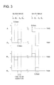
- a monochrome display having 2x2 pixels as shown in Fig. 2 is used for an example to explain the wave pattern of driving voltage.
- FIG.3 an example of a wave pattern of driving voltage to display or erase a pixel according to the conventional method in such a display element in which a negative voltage is applied to a column electrode, and when the voltage becomes larger than the deposition threshold potential, deposition of silver occurs on the column electrode, while, when a positive voltage is applied to the column electrode, the deposited silver is dissolved.
- Fig. 3 shows row voltages applied to the row electrodes A 1 , A 2 and column voltages applied to the column electrodes B 1 , B 2 .
- a scanning voltage which is smaller than the deposition threshold potential is applied to each of the row electrodes A 1 , A 2 and an address pulse voltage for signal writing, which is smaller than the deposition threshold potential, is applied to each of the column electrode B 1 , B 2 .
- the selection operation is carried out sequentially from the top.
- a larger voltage than deposition threshold potential is applied only to the pixel to have silver deposition, thus, silver is deposited on the column electrode to form silver nuclei.
- the address pulse voltage applied to the column electrode B 1 and the address pulse voltage applied to the row electrode A 1 are added to apply a voltage larger than the deposition threshold potential to the pixel.
- silver is deposited and thus black display is carried out.
- the pixel (A 1 , B 2 ) there is no period when the address pulse voltage of the column electrode and the address pulse voltage of the row electrode is added, and only a voltage lower than the deposition threshold potential is applied to the pixel. Therefore, since no deposition of silver occurs, it serves as a white display.
- a data sustaining pulse voltage to the row electrodes A 1 , A 2 , ⁇ , ⁇ in the data sustaining period after the data address period.
- the amount of deposited silver can be controlled by applying the data sustaining pulse voltage to uniformize the density of each pixel.
- a data sustaining pulse voltage is applied, deposition of silver is continued only in the pixel to which a voltage larger than the deposition threshold potential has been applied, and in the pixel to which no such high voltage larger than the deposition threshold potential has been applied, no deposition of silver occurs even when the data sustaining pulse voltage Vsus is applied, and no-deposition state is maintained.
- Conversion of the black display of the image (A 1 , B 1 ) to a white display is carried out by reversing the polarity of each of the address pulse voltage of the column electrode and the address pulse voltage of the row electrode, whereby deposited silver is dissolved again to give a white display.
- conversion of the black display to the white display namely a whitening operation, has been carried out independently in each black display pixel in a similar manner as the blackening operation.
- the display element and its driving method of the present invention is characterized in that at least two pixels each having a different extent of blackening are simultaneously reset to white.
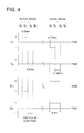
- Fig. 4 illustrates an example of a wave pattern of driving voltage used for the driving method of the display element of the present invention.
- conversion to white display is carried out by scanning the row electrodes (A 1 , A 2 ), but, not by selectively scanning the column electrodes.
- the whitening operation is carried by applying an address pulse voltage (positive voltage) necessary to whitening uniformly to all the column electrodes. As the result, the driving time is shortened, since no selective scanning is carried out, and also because electric current is supplied to the neighboring pixels.
- Fig. 5 illustrates another example of a wave pattern of driving voltage used for the driving method of the display element of the present invention.
- conversion to white display is carried out by applying a negative address pulse voltage to all the row electrodes (A 1 , A 2 ) and applying a positive address pulse voltage to all the column electrodes (B 1 , B 2 ), without scanning the row electrodes (A 1 , A 2 ) and the column electrodes (B 1 , B 2 ) .
- the driving time is shortened, since no selective scanning of each of the row electrodes (A 1 , A 2 ) and the column electrodes (B 1 , B 2 ) is carried out, and also because electric current is supplied to the neighboring pixels.
- the electrolyte layer preferably contains at least one compound represented by above mentioned Formula (1) or Formula (2) and at least one compound represented by above mentioned Formula (3) and Formula (4)
- L represents an oxygen atom or CH 2
- R 1 - R 4 each represent a hydrogen atom, an alkyl group, an alkenyl group, an aryl group, a cycloalkyl group, an alkoxy alkyl group or an alkoxy group.
- Examples of an alkyl group include: a methyl group, an ethyl group, a propyl group, an isopropyl group, a tert-butyl group, a pentyl group, a hexyl group, an octyl group, a dodecyl group, a tridecyl group, a tetradecyl group and a pentadecyl group;
- examples of an aryl group include: a phenyl group and a naphthyl group;
- examples of a cycloalkyl group include: a cyclopentyl group and a cyclohexyl group;
- examples of an alkoxyalkyl group include: ⁇ -methoxyethyl group and ⁇ -methoxypropyl group; and examples of an alkoxy group include: a methoxy group, an ethoxy group, a propyloxy group, a pentyl
- the compounds represented by Formula (1) are commercially available, for example, propylene carbonate produced by Showa Denko K. K. and propylene carbonate produced by Kanto Chemical Co., Inc. Also, these compounds can be synthesized according to the method given in AIST Today, 2003, 05 Vol. 3-5.
- R 5 , R 6 each represent a hydrogen atom, an alkyl group, an alkenyl group, an aryl group, a cycloalkyl group, an alkoxyalkyl group or an alkoxy group.
- Examples of an alkyl group include: a methyl group, an ethyl group, a propyl group, an isopropyl group, a tert-butyl group, a pentyl group, a hexyl group, an octyl group, a dodecyl group, a tridecyl group, a tetradecyl group and a pentadecyl group;
- examples of an aryl group include: a phenyl group and a naphthyl group;
- examples of a cycloalkyl group include: a cyclopentyl group and a cyclohexyl group;
- examples of an alkoxyalkyl group include: ⁇ -methoxyethyl group and ⁇ -methoxypropyl group; and examples of an alkoxy group include: a methoxy group, an ethoxy group, a propyloxy group, a pentyl
- the compounds represented by Formula (2) are commercially available, for example, ethylene carbonate produced by Maruzen Petrochemical Co., Ltd. and ethylene carbonate produced by Kanto Chemical Co., Inc. Also, these compounds can be synthesized according to the method given in AIST Today, 2003, 05 Vol. 3-5 .
- the compounds represented by Formula (1) and Formula (2) of the present invention belong to one sort of an electrolyte solvent.
- another solvent can be used in combination, provided that the object effect of the present invention is not lost.
- a solvent include: tetramethylurea, sulfolane, dimethyl sulfoxide, 1,3-dimethyl-2-imidazolidinone, 2-(N-methyl)-2-pyrrolidinone, hexamethylphosphortriamide, N-methyl propione amide, N,N-dimethylacetamide, N-methylacetamide, N,N-dimethylformamide, N-methylformamide, butyronitrile, propionitrile, acetonitrile, acetylacetone, 4-methyl-2-pentanone, 2-butanol, 1-butanol, 2-propanol, 1-propanol, ethanol, methanol, acetic anhydride, ethylacetate, ethylpropionate
- At least one solvent having a freezing point of -20 °C or lower and a boiling point of 120 °C or more is incorporated.
- solvent employable in the present invention are the compounds shown in: J.A.Riddick, W.B.Bunger, T.KSakano, "Organic Solvents", 4th. ed., John Wiley & Sons (1986 ), Y.Marcus, “Ion Solvation”, John Wiley & Sons (1985 ), C. Reichardt, "Solvents and Solvent Effects in Chemistry", 2nd ed., VCH (1988 ) and G.J. Janz, R.P.T.Tomkins, "Nonaqueous Electorlytes Handbook", Vol.1, Academic Press (1972 ).
- the electrolyte solvent may be a single kind or may be a mixture, however, a mixed solvent containing ethylene carbonate is preferable.
- the added amount of ethylene carbonate is preferably 10 mass % or more but 90 mass % or less.
- a mixed electrolyte solvent having a propylene carbonate/ethylene carbonate mass ratio of 7/3 to 3/7 is specifically preferable. When the propylene carbonate mass ratio is larger than 7/3, ionic conductivity of the electrolyte may become lower, resulting in decrease of response rate, while when it is smaller than 3/7, deposition of electrolyte tends to occur at a lower temperature.
- R 7 and R 8 each represent a substituted or unsubstituted hydrocarbon group, which may contain a normal chain group or a branched chain group of an aromatic compound.
- the hydrocarbon group may contain one or more nitrogen atoms, oxygen atoms, phosphorus atoms, sulfur atoms, or halogen atoms, provided that, when a ring containing S atom is formed, no aromatic group is contained.
- Examples of a substituent of the hydrocarbon group include an amino group, a guanidino group, a quarternary ammonium group, a hydroxyl group, a halogen compound, a carboxylic acid group, a carboxylate group, an amide group, a sulfinic acid group, a sulfonic acid group, a sulfate group, a phosphonic acid group, a phosphate group, a nitro group and a cyano group.
- a method by which silver or a compound containing silver is converted to a soluble compound by coexisting silver or a compound containing silver with a compound having a chemical structure which can interact with silver, for example, to form a coordinate bond with silver or to form a weak covalent bond with silver.
- a chemical structure include: a halogen atom, a mercapto group, a carboxyl group and an imino group.
- a thioether group is also useful and works as a silver resolvent having less influence to the coexixting compounds and a high solbility to the solvent.
- the compounds represented by Formula (3) are commercially available, for example, 3-thia-1,5-pentanediol produced by Kanto Chemical Co., Inc. Also, these compounds can be synthesized according to the method given in US Patent No. 4126459 or JP-A No. 2003-267899 .
- exemplified compound (3-2) is specifically preferable to fully achieve the effect of the present invention.
- M represents a hydrogen atom, a metal atom or a quarternary ammonium
- Z represents a nitrogen-containing heterocyle, provided that Z is not an imidazole ring
- n represents an integer of 0 to 5
- R 9 represents a hydrogen atom, a halogen atom, an alkyl group, an aryl group, an alkylcarbonamide group, an arylcarbonamide group, an alkylsulfonamide group, an arylsulfonamide group, an alkoxy group, an aryloxy group, an alkylthio group, an arylthio group, an alkylcarbamoyl group, an arylcarbamoyl group, a carbamoyl group, an alkylsulfamoyl group, an arylsulfamoyl group, a sulfamoyl group, a cyano group, an alkylsulfonyl group, an aryls
- Examples of a metal atom represented by M include Li, Na, K, Mg, Ca, Zn and Ag.
- Examples of a quarternary ammonium include NH 4 , N(CH 3 ) 4 , N(C 4 H 9 ) 4 , N(CH 3 ) 3 C 12 H 25 , N(CH 3 ) 3 C 16 H 33 , and N (CH 3 ) 3 CH 2 C 6 H 5 .
- Examples of a nitrogen-containing heterocyclic ring represented by Z in Formula (4) include a tetrazole ring, a triazole ring, an oxydiazole ring, a thiadiazole ring, an indole ring, an oxazole ring, a benzoxazole ring, a benzothiazole ring, a benzoselenazole ring and a naphthoxazole ring.
- R 9 represents one of the atoms or groups listed below:
- the compounds represented by Formula (4) are commercially available, for example, 2-mercaptobenzoxazole produced by Tokyo Chemical Industry Co. Also, these compounds can be synthesized according to the method disclosed in JP-A No. 1-4739 or No. 3-10172 .
- exemplified compounds (4-12) and (4-18) are specifically preferable to fully achieve the effect of the present invention.
- a halogen atom means an iodine atom, a chlorine atom, a bromine atom or a fluorine atom.
- the molar content of halogen is preferably as low as possible against the molar content of silver. In the present invention, more preferable is 0 ⁇ [X] / [Ag] ⁇ 0.001.
- the total molar content of each halogen species preferably satisfies [I] ⁇ [Br] ⁇ [Cl] ⁇ [F].
- the present invention is characterized in that the electrolyte layer contains substantially no iodine.
- substantially no iodine means, in the present invention, that, when a molar content of iodine ions or iodine atoms contained in the electrolyte layer of the display element is represented as [I] (mole/kg) and a total molar content of silver or silver contained in the compound having silver in the chemical structure is represented as [Ag] (mole/kg), it is preferable that following Condition (2) is satisfied: 0 ⁇ X / Ag ⁇ 0.001
- the yellowish stain due to the oxidized iondine contained in the electrolyte layer can be avoided, even when an excessive voltage is applied to each pixel to whiten the pixel.
- silver salts known in the art can be used.
- examples of such silver salts include: silver iodide, silver chloride, silver bromide, silver oxide, silver sulfide, silver citrate, silver acetate, silver behenate, a silver salt of p-toluenesulfonic acid, a silver salt of mercapto compound and a silver complex with an iminodiacetic acid.
- a silver salt which does not contain a nitrogen atom having coordinating property with halogen, carboxylic acid or silver for example, a silver salt of p-toluenesulfonic acid is preferable.
- the content of silver ions in the electrolyte layer of the present invention is preferably 0.2 mole/kg ⁇ [Ag] ⁇ 2.0 mole/kg.
- the content of silver ions is smaller than 0.2 mole/kg, the silver solution becomes too diluted and the driving rate is reduced, while, when the content of silver ions is larger than 2 mole/kg, the solubility becomes too low, and precipitation tends to occur while stored at a lower temperature, which is disadvantageous.
- electrolytes when electrolytes are in liquid form, it is possible to incorporate, in the electrolytes, the following compounds.
- potassium compounds are KCl, KI, and KBr; listed as lithium compounds are LiBF 4 , LiClO 4 , LiPF 6 , and LiCF 3 SO 3 ; while listed as tetraalkylammonium compounds are tetraethylammonium perchlorate, tetrabutylammonium perchlorate, tetraethylammonim borofluoride, tetrabutylammonium borofluoride, and tetrabutylammonium halide.
- fused salt electrolyte compositions described in paragraphs [0062] - [0081] of JP-A No. 2003-187881 are fused salt electrolyte compositions described in paragraphs [0062] - [0081] of JP-A No. 2003-187881 .
- Further employed are compounds which form oxidation-reduction pairs such as I - /I 3 - , Br - /Br 3 - and quinone/hydroquinone.
- electrolytes when electrolytes are in solid form, it is possible to incorporate, in the electrolytes, the following compounds which exhibit electronic or ionic conductivity.
- fluorinated vinyl based polymers containing perfluorosulfonic acid polythiophene; polyaniline; polypyrrole, triphenylamines; polyvinylcarbazoles; polymethylphenylsilanes; calcogenides such as Cu 2 S, Ag 2 S, Cu 2 Se, or AgCrSe 2 ; fluorine compounds such as CaF 2 , PbF 2 , SrF 2 , LaF 3 , TlSn 2 F 5 , or CeF 3 ; lithium salts such as Li 2 SO 4 or Li 4 SiO 4 ; as well as compounds such as ZrO 2 , CaO, Cd 2 O 3 , HfO 2 , Y 2 O 3 , Nb 2 O 5 , WO 3 , Bi 2 O 3 , AgBr, AgI, CuCl, CuBr, CuBr, CuI, LiI, LiBr, LiCl, LiAlCl 4 , LiAlF 4 , AgSB
- electrolytes in gel form.
- electrolytes are nonaqueous, it is possible to employ oil gelling agents described in paragraphs [0057] - [0059] of JP-A No. 11-185836 .
- the electrolyte layer incorporates white particles.
- white particles include: titanium dioxide (an anatase type or a rutile type), barium sulfate, calcium carbonate, aluminum oxide, zinc oxide, magnesium oxide, zinc hydroxide, magnesium hydroxide, magnesium phosphate, magnesium hydrogenphosphate, alkaline earth metal salts, talc, kaolin, zeolite, acid clay, glass, as well as organic compounds such as polyethylene, polystyrene, acryl resins, ionomers, ethylene-vinyl acetate copolymer resins, benzoguanamine resins, urea-formalin resins, melamine-formalin resins, or polyamide resins. These particle may be used alone or in combination. Also, the particles may contain voids to alter the refractive index.
- titanium dioxide preferably employed are titanium dioxide, zinc oxide, and zinc hydroxide.
- titanium dioxide which has been subjected to a surface treatment employing inorganic oxides (for example, Al 2 O 3 , AlO(OH), and SiO 2 ).
- titanium dioxide particles may be subjected to a treatment employing organic compounds such as trimethylolethane, triethanolamine acetic acid salts or trimethylcyclosilane.
- titanium oxide or zinc oxide are preferably used in order to prevent coloring at a higher temperature or with respect to the reflectance of the display element which is influenced by the refractive index.
- thickening agents in the electrolyte layer.
- thickening agents include gelatin, gum Arabic, poly(vinyl alcohol), hydroxyethyl cellulose, hydroxypropyl cellulose, cellulose acetate, cellulose acetate butyrate, poly(vinylpyrrolidone), poly(alkylene glycol), casein, starch, poly(acrylic acid), poly(methylmethacrylic acid), poly(vinyl chloride), poly(methacrylic acid), copoly(styrene-maleic anhydride), copoly(styrene-acrylonitrile), copoly(styrene-butadiene), poly(vinyl acetals) (for example, poly(vinyl formal), poly(vinyl butyral)), poly(vinyl esters), poly(urethanes), phenoxy resins, poly(vinylidene chloride), poly(epoxides), poly(carbonates), poly(vinyl
- thickening agents may be employed in combinations of at least two types. Further listed are the compounds described on pages 71 - 75 of JP-A No. 64-13546 . Of these, in view of compatibility with various types of additives and enhancement of dispersion stability of white particles, preferably employed compounds are polyvinyl alcohols, polyvinylpyrrolidones, hydroxypropyl celluloses, and polyalkylene glycols.
- constitution layers include ancillary layers such as a protective layer, a filter layer, an antihalation layer, a cross-over light cutting layer, or a backing layer.
- ancillary layers may be various chemical sensitizers, noble metal sensitizers, photosensitive dyes, supersensitizers, couplers, high boiling point solvents, antifoggants, stabilizers, development inhibitors, bleach accelerators, fixing accelerators, color mixing inhibitors, formalin scavengers, toners, hardeners, surface active agents, thickening agents, plasticizers, lubricants, UV absorbers, antirradiation dyes, filter light absorbing dyes, mildewcides, polymer latexes, heavy metals, antistatic agents, and matting agents.
- RD Volume 176 Item/17643 (December 1978 ), RD Volume 184 Item/18431 (March 1979 ), DR Volume 187 Item/18716 (November 1979 ), and RD Volume 308 Item/308119 (December 1989 ).
- positive hole transport materials include aromatic amines, triphenylene derivatives, oligochiophene compounds, polypyrroles, polyacetylene derivatives, polyphenylene vinylene derivatives, polythienylene vinylene derivatives, polythiophene derivatives, polyaniline derivatives, polytoluidine derivatives, CuI, CUSCN, CuInSe 2 , Cu(In,Ga)Se, CuGaSe 2 , Cu 2 O, CuS, CuGaS 2 , CuInS 2 , CuAlSe 2 , GaP, NiO, CoO, FeO, Bi 2 O 3 , MoO 2 , and Cr 2 O 3 .
- Examples of a support employable in the display element of the present invention include: polyolefins such as polyethylene or polypropylene, polycarbonates, cellulose acetate, polyethylene terephthalate, polyethylene dinaphthalene dicarboxylate, polystyrene naphthalates, polyvinyl chloride, polyimide, polyvinyl acetals, and polystyrene.
- polyolefins such as polyethylene or polypropylene
- polycarbonates such as polyethylene or polypropylene, polycarbonates, cellulose acetate, polyethylene terephthalate, polyethylene dinaphthalene dicarboxylate, polystyrene naphthalates, polyvinyl chloride, polyimide, polyvinyl acetals, and polystyrene.
- syndioctatic structured polystyrenes are prepared employing the methods described, for example, in each of JP-A Nos. 62-117708 , 1-46912
- metal substrates including stainless steel, paper supports such as baryta paper or resin coated paper, supports including the above plastic film having thereon a reflection layer, and those which are described in JP-A No. 62-253195 (pages 29 - 31) as a support. Further preferably employed are those described on page 28 of RD No. 17643, from the right column to the left column on page 648 of RD No. 18716, and on page 879 of RD No. 307105. As described in U.S. Patent No. 4,142,735 , these supports may be subjected to a thermal treatment at a temperature lower than Tg so that core-set curl is decreased.
- the surface of these supports may be subjected to a surface treatment with the aim of enhancement of adhesion of the support to other constituting layers.
- employed as surface treatments may be a glow discharge treatment, an ultraviolet radiation irradiation treatment, a corona treatment and a flame treatment.
- Further employed may be supports described on pages 44 - 149 of Kochi Gijutsu (Prior Art Technology) No. 5 (published by AZTEC Corp., dated March 22, 1991 ). Further listed are those described on page 1009 of RD No. 308119, as well as in the item " Supports" on page 108 of Product Licensing Index Volume 92 .
- employed may be glass substrates as well as epoxy resins kneaded with glass powder.
- At least one of the opposed electrodes is a metal electrode.
- metal electrodes may be metals such as platinum, gold, silver, copper, aluminum, zinc, nickel, titanium, or bismuth, as well as alloys thereof, which are known in the art.
- Preferred metals employed in the metal electrodes are those which exhibit a work function near the oxidation-reduction potential of silver in electrolytes.
- a silver electrode or an electrode composed of silver in an amount of at least 80 percent is advantageous to maintain a reduced state of silver, and in addition, results in anti-staining of electrodes.
- Employed as methods for preparing electrodes may be conventional ones such as a evaporating method, a printing method, an ink-jet method, a spin coating method, or a CVD method.
- At least one of the opposed electrodes is a transparent electrode.
- Transparent electrodes are not particularly limited as long as they are transparent and electrically conductive. Examples include indium tin oxide (ITO), indium zinc oxide (IZO), tin oxide, fluorine-containing tin oxide (FTO), indium oxide, zinc oxide, platinum, gold, silver rhodium, copper, chromium, carbon, aluminum, silicon, amorphous silicon, and BSO (bismuth silicon oxide).
- an ITO layer may be subjected to mask evaporation on a substrate employing a sputtering method, or after forming an ITO layer on the entire surface, patterning may be performed employing a photolithographic method.
- the surface resistance value is preferably 100 ⁇ /sq or less, but is more preferably 10 ⁇ /sq or less.
- the thickness of the transparent electrodes is not particularly limited but is commonly 0.1 - 20 ⁇ m.
- employed in the display element of the present invention may be sealing agents, column-structured materials, and spacer particles.
- Sealing agents are those to seal materials so that they do not leak out.
- Employed as sealing agents may be heat curing, light curing, moisture curing, and anaerobic curing type resins such as epoxy resins, urethane resins, acryl resins, vinyl acetate resins, enethiol resins, silicone resins, or modified polymer resins.
- Column-structured materials provides strong self-supporting (strength) between substrates.
- listed may be a cylindrical form, a quadrangular form, an elliptic cylindrical form, and a trapezoidal form which are arranged at definite intervals in a specified pattern such as a lattice. Further, employed may be stripe-shaped ones arranged at definite intervals.
- the column-structured materials are not randomly arranged but arranged at an equal distance, arranged so that the interval gradually varies, or a predetermined pattern is repeated at a definite cycle so that the distance between substrates is appropriately maintained and image display is not hindered.
- the column-structured materials are such that the ratio of the area occupied by the display region of a display element is 1 - 40 percent, sufficient strength for commercial viability is obtained as a display element.
- spacers between them In order to maintain a uniform gap between paired substrates, provided may be spacers between them. As such spacers, exemplified may be spheres composed of resins or inorganic oxides. Further, suitably employed are adhesion spacers the surface of which is coated with thermoplastic resins. In order to maintain the uniform gap between substrates, provided may only be column-structured materials. However, both spacers and column-structure materials may be provided. In place of the column-structured materials, only spacers may be employed as a space- maintaining member. The diameter of spacers, when a column-structured material is formed, is at most its height, but is preferably equal to the height. When the column-structured material is not formed, the diameter of spacers corresponds to the distance of the cell gap.
- sealing agents In the present invention, it is possible to form sealing agents, column-structured materials, and electrode patterns, employing a screen printing method.
- screen printing methods a screen on which predetermined patterns are formed is covered on the electrode surface, and printing materials (compositions to form column-structured materials such as light-curing resins) are placed on the screen. Subsequently a squeegee is moved at predetermined pressure, angle and rate. By such action, the printing materials are transferred onto the above substrate via the pattern of the screen. Then, the transferred materials are thermally cured and dried.
- resinous materials are not limited to light-curing resins, but also employed, for example, may be heat curable resins such as epoxy resins or acryl resins, as well as thermoplastic resins.
- thermoplastic resins are polyvinyl chloride resins, polyvinylidene chloride resins, polyvinyl acetate resins, polymethacrylic acid ester resins, polyacrylic acid ester resins, polystyrene resins, polyamide resins, polyethylene resins, polypropylene resins, fluorocarbon resins, polyurethane resins, polyacrylonitrile resins, polyvinyl ether resins, polyvinylketone resins, polyether resins, polyvinylpyrrolidone resins, saturated polyester resins, polycarbonate resins, and chlorinated polyether resins. It is preferable that resinous materials are employed in the form of a paste while dissolved in suitable solvents.
- spacers are provided on at least one side of the substrate, and paired substrates are placed so that the electrode forming surfaces face each other, whereby a vacant cell is formed.
- paired substrates are placed so that the electrode forming surfaces face each other, whereby a vacant cell is formed.
- Preparation of a display element may be performed by injecting an electrolyte composition between the substrates, employing a vacuum injection method.
- an electrolyte composition may be dripped on the surface of one of the substrates and then liquid crystal composition may be sealed simultaneously when the substratres are allowed to adhere to each other.
- the preferable driving operation include depositing blackened silver by applying a voltage larger than the deposition overpotential potential to the pixel, followed by continuing the deposition of blackened silver by applying a voltage lower than the deposition overpotential potential to the pixel.
- the overpotentioal is found page 121 of "Denshi-ido no kagaku - Denkikagaku Nyuumon" (1996, Asakura Publishing Co., Ltd. ).
- the between the electrode and silver contained in the electrolyte is considered to be an electrochemical reaction, and it is easily understood that an overpotential exists when the dissolution and deposition of silver are carried out.
- the extent of an overpotential depends on the exchange current density. Accordingly, it can be deduced that the surface of blackened silver has less excess electrical energy and injection of electrons is more easily carried out, because deposition of blackened silver can be continued at a lower applying voltage than the deposition overpotential of silver.
- the driving operation of the display element of the present invention may be via a simple matrix drive or an active matrix drive.
- “Simple matrix drive”, as described in the present invention, refers to the driving method in which a plurality of positive electrode lines and a plurality of negative electrode lines are placed face to face so that the positive electrode lines and the negative electrode lines cross in right angles, and electric current is sequentially applied to these positive electrode lines and negative electrode lines.
- By employing the simple matrix driving it is possible to simplify the circuit structure and the driving IC, resulting in advantages such as lower production cost.
- Active matrix drive refers to a system in which scanning lines, data lines, and current feeding lines are formed in a checkered pattern and driving is performed by TFT circuits arranged in each of the squares of the checkered pattern. Since switching is performed for each pixel, advantages result in gradation as well as memory function. For example, a circuit disclosed in Fig. 5 of JP-A No. 2004-29327 is usable.
- the display element of the present invention can be applied to electronic book related field, ID card related fields, public information related fields, transportation related fields, broadcasting related fields, account settling fields, and distribution and logistics related fields.
- Specific examples include door keys, student identification cards, corporate member identification cards, various club membership cards, convenience store cards, department store cards, vending machine cards, gas station cards, subway and railroad cards, bus cards, cash cards, credit cards, highway cards, driver licenses, hospital medical examination cards, health insurance cards, residents' basic registers, passports and electronic books.
- Silver paste ink (produced by TOYOBO Co., Ltd.) was screen printed with a thickness of 10 ⁇ m so as to form lines of 4 mm width with 1 mm interval on a 1.5 mm thick 2 cm x 4 cm glass substrate and heated for 30 minutes in a vacuum oven at 150 °C, whereby a silver electrode (Electrode 2) was obtained.
- Electrolyte liquid 3 was prepared in the same manner as Electrolyte liquid 2, except that dimethylsulfoxide was used instead of propylene carbonate/ethylene carbonate.
- Electrolyte liquid 4 was prepared in the same manner as Electrolyte liquid 3, except that 3,6-dithia-1,8-octanediol was not used and 300 mg of mercaptotriazole was used.
- Electrolyte liquid 5 was prepared in the same manner as Electrolyte liquid 3, except that mercaptotriazole was not used.
- Electrolyte liquid 6 was prepared in the same manner as Electrolyte liquid 2, except that silver bromide was used instead of silver p-toluenesulfonate.
- Electrolyte liquid 7 was prepared in the same manner as Electrolyte liquid 2, except that silver chloride was used instead of silver p-toluenesulfonate.
- Display Elements 2 - 7 were prepared in the same manner as Display Element 1, except that Electrolyte liquids 2 - 7 were used instead of Electrolyte liquid 1.
- dissolution - deposition reaction of silver in the electrolyte was carried out with an electricity of 5 mC/cm 2 per pixel to switch white display (dissolution state of silver) and black display (deposit state of silver).
- Display Element 1 which is a comparative example did not give a W2/W1 value close to 1.0 due to the effect of the yellowish stain.
- whitening of the pixels was completed with 1 pulse applying time of shorter than 1.6 when the driving method prescribed in the present invention was used. Accordingly, it was confirmed that the display elements of the present invention having the construction prescribed by the present invention have superior whole display resetting property to white display compared to the comparative display elements.
Landscapes
- Physics & Mathematics (AREA)
- Nonlinear Science (AREA)
- General Physics & Mathematics (AREA)
- Engineering & Computer Science (AREA)
- Chemical & Material Sciences (AREA)
- Inorganic Chemistry (AREA)
- Optics & Photonics (AREA)
- Computer Hardware Design (AREA)
- Theoretical Computer Science (AREA)
- Electrochromic Elements, Electrophoresis, Or Variable Reflection Or Absorption Elements (AREA)
- Control Of Indicators Other Than Cathode Ray Tubes (AREA)
- Devices For Indicating Variable Information By Combining Individual Elements (AREA)
Applications Claiming Priority (2)
| Application Number | Priority Date | Filing Date | Title |
|---|---|---|---|
| JP2005028671 | 2005-02-04 | ||
| PCT/JP2006/300244 WO2006082697A1 (fr) | 2005-02-04 | 2006-01-12 | Élément d’affichage et méthode de pilotage de celui-ci |
Publications (2)
| Publication Number | Publication Date |
|---|---|
| EP1845410A1 true EP1845410A1 (fr) | 2007-10-17 |
| EP1845410A4 EP1845410A4 (fr) | 2009-02-11 |
Family
ID=36777086
Family Applications (1)
| Application Number | Title | Priority Date | Filing Date |
|---|---|---|---|
| EP06702561A Withdrawn EP1845410A4 (fr) | 2005-02-04 | 2006-01-12 | Element d'affichage et methode de pilotage de celui-ci |
Country Status (4)
| Country | Link |
|---|---|
| US (1) | US7602543B2 (fr) |
| EP (1) | EP1845410A4 (fr) |
| JP (1) | JP4968061B2 (fr) |
| WO (1) | WO2006082697A1 (fr) |
Cited By (1)
| Publication number | Priority date | Publication date | Assignee | Title |
|---|---|---|---|---|
| US7602543B2 (en) * | 2005-02-04 | 2009-10-13 | Konica Minolta Holdings, Inc. | Display element and driving method thereof |
Families Citing this family (7)
| Publication number | Priority date | Publication date | Assignee | Title |
|---|---|---|---|---|
| EP1950607B1 (fr) * | 2005-11-17 | 2010-06-16 | Konica Minolta Holdings, Inc. | Procédé de production d'un élément d'affichage |
| EP1975692A4 (fr) * | 2006-01-19 | 2009-01-14 | Konica Minolta Holdings Inc | Element d'affichage |
| JP5083307B2 (ja) * | 2007-02-21 | 2012-11-28 | コニカミノルタホールディングス株式会社 | 表示素子の駆動方法 |
| JP5381720B2 (ja) * | 2008-02-22 | 2014-01-08 | コニカミノルタ株式会社 | 表示装置、表示装置の制御方法 |
| JP4666118B2 (ja) * | 2009-06-16 | 2011-04-06 | コニカミノルタホールディングス株式会社 | 電気化学表示素子の駆動方法および情報表示装置 |
| JP2012238444A (ja) * | 2011-05-11 | 2012-12-06 | Seiko Epson Corp | 高分子固体電解質及びその製造方法、リチウムイオン二次電池 |
| WO2018213411A1 (fr) | 2017-05-17 | 2018-11-22 | University Of South Florida | Dispositifs électrochromiques à couche active unique |
Citations (2)
| Publication number | Priority date | Publication date | Assignee | Title |
|---|---|---|---|---|
| JP2004177491A (ja) * | 2002-11-25 | 2004-06-24 | Sony Corp | エレクトロデポジション型表示装置とその駆動方法 |
| JP2004191838A (ja) * | 2002-12-13 | 2004-07-08 | Sony Corp | 電気化学表示装置及びその製造方法 |
Family Cites Families (10)
| Publication number | Priority date | Publication date | Assignee | Title |
|---|---|---|---|---|
| US4240716A (en) | 1978-12-15 | 1980-12-23 | Bell Telephone Laboratories, Incorporated | Electrodeposition display device |
| US5764401A (en) * | 1994-11-11 | 1998-06-09 | Sony Corporation | Optical apparatus |
| JPH11142895A (ja) * | 1997-09-08 | 1999-05-28 | Sony Corp | 光学装置及び電解液 |
| JP2003241227A (ja) | 2002-02-14 | 2003-08-27 | Sony Corp | 電気化学表示素子及び電気化学表示装置 |
| JP4356283B2 (ja) * | 2002-05-20 | 2009-11-04 | ソニー株式会社 | 表示素子の駆動方法 |
| JP4508544B2 (ja) * | 2003-04-07 | 2010-07-21 | ソニー株式会社 | 電気化学表示装置 |
| EP1845410A4 (fr) * | 2005-02-04 | 2009-02-11 | Konica Minolta Holdings Inc | Element d'affichage et methode de pilotage de celui-ci |
| JP5003485B2 (ja) * | 2005-05-31 | 2012-08-15 | コニカミノルタホールディングス株式会社 | 表示素子 |
| EP1887419A4 (fr) * | 2005-06-02 | 2008-09-17 | Konica Minolta Holdings Inc | Élément d´affichage |
| WO2007010653A1 (fr) * | 2005-07-19 | 2007-01-25 | Konica Minolta Holding, Inc. | Sel fondu a temperature ambiante et dispositif d'affichage |
-
2006
- 2006-01-12 EP EP06702561A patent/EP1845410A4/fr not_active Withdrawn
- 2006-01-12 WO PCT/JP2006/300244 patent/WO2006082697A1/fr active Application Filing
- 2006-01-12 JP JP2007501519A patent/JP4968061B2/ja not_active Expired - Fee Related
- 2006-01-12 US US11/883,455 patent/US7602543B2/en not_active Expired - Fee Related
Patent Citations (2)
| Publication number | Priority date | Publication date | Assignee | Title |
|---|---|---|---|---|
| JP2004177491A (ja) * | 2002-11-25 | 2004-06-24 | Sony Corp | エレクトロデポジション型表示装置とその駆動方法 |
| JP2004191838A (ja) * | 2002-12-13 | 2004-07-08 | Sony Corp | 電気化学表示装置及びその製造方法 |
Non-Patent Citations (1)
| Title |
|---|
| See also references of WO2006082697A1 * |
Cited By (1)
| Publication number | Priority date | Publication date | Assignee | Title |
|---|---|---|---|---|
| US7602543B2 (en) * | 2005-02-04 | 2009-10-13 | Konica Minolta Holdings, Inc. | Display element and driving method thereof |
Also Published As
| Publication number | Publication date |
|---|---|
| EP1845410A4 (fr) | 2009-02-11 |
| US20080170288A1 (en) | 2008-07-17 |
| JP4968061B2 (ja) | 2012-07-04 |
| US7602543B2 (en) | 2009-10-13 |
| WO2006082697A1 (fr) | 2006-08-10 |
| JPWO2006082697A1 (ja) | 2008-06-26 |
Similar Documents
| Publication | Publication Date | Title |
|---|---|---|
| US7184198B2 (en) | Display element | |
| JP4905353B2 (ja) | 表示素子の駆動方法 | |
| EP1887419A1 (fr) | Élément d´affichage | |
| JP4876921B2 (ja) | 表示素子 | |
| US8264423B2 (en) | Method of driving display element | |
| US7602543B2 (en) | Display element and driving method thereof | |
| JP5003485B2 (ja) | 表示素子 | |
| US7864407B2 (en) | Display element | |
| EP1950607A1 (fr) | Element d'affichage et procede de production associe | |
| JP2006227488A (ja) | 表示素子 | |
| JP4876544B2 (ja) | 表示素子 | |
| EP2028539B1 (fr) | Element d'affichage | |
| JP2007264011A (ja) | 表示素子 | |
| JP2007199147A (ja) | 表示素子 | |
| JP2007072368A (ja) | 表示素子 | |
| JP4569425B2 (ja) | 表示素子 | |
| JP2007025218A (ja) | 表示素子の作製方法 | |
| JP2007025219A (ja) | 表示素子 | |
| JP4997807B2 (ja) | 多孔質白色散乱層の形成方法及び表示素子 | |
| JP2007025327A (ja) | 表示素子 | |
| JP2006227254A (ja) | 電気化学トランジスタ、及びこれを用いた表示素子 | |
| JP2008185684A (ja) | 表示素子 | |
| JP2008003279A (ja) | 表示素子 | |
| JP2008122829A (ja) | 表示素子 |
Legal Events
| Date | Code | Title | Description |
|---|---|---|---|
| PUAI | Public reference made under article 153(3) epc to a published international application that has entered the european phase |
Free format text: ORIGINAL CODE: 0009012 |
|
| 17P | Request for examination filed |
Effective date: 20070711 |
|
| AK | Designated contracting states |
Kind code of ref document: A1 Designated state(s): AT BE BG CH CY CZ DE DK EE ES FI FR GB GR HU IE IS IT LI LT LU LV MC NL PL PT RO SE SI SK TR |
|
| DAX | Request for extension of the european patent (deleted) | ||
| A4 | Supplementary search report drawn up and despatched |
Effective date: 20090113 |
|
| STAA | Information on the status of an ep patent application or granted ep patent |
Free format text: STATUS: THE APPLICATION HAS BEEN WITHDRAWN |
|
| 18W | Application withdrawn |
Effective date: 20090831 |