EP1840582A1 - Resonating inertial micro-sensor with variable thickness made using surface technologies - Google Patents
Resonating inertial micro-sensor with variable thickness made using surface technologies Download PDFInfo
- Publication number
- EP1840582A1 EP1840582A1 EP07104737A EP07104737A EP1840582A1 EP 1840582 A1 EP1840582 A1 EP 1840582A1 EP 07104737 A EP07104737 A EP 07104737A EP 07104737 A EP07104737 A EP 07104737A EP 1840582 A1 EP1840582 A1 EP 1840582A1
- Authority
- EP
- European Patent Office
- Prior art keywords
- zone
- thickness
- resonator
- sensor
- hinge
- Prior art date
- Legal status (The legal status is an assumption and is not a legal conclusion. Google has not performed a legal analysis and makes no representation as to the accuracy of the status listed.)
- Granted
Links
- 238000005516 engineering process Methods 0.000 title description 19
- 238000000034 method Methods 0.000 claims abstract description 30
- 238000001514 detection method Methods 0.000 claims abstract description 29
- 238000005530 etching Methods 0.000 claims abstract description 29
- 239000000758 substrate Substances 0.000 claims abstract description 15
- 238000006073 displacement reaction Methods 0.000 claims abstract description 8
- 239000010410 layer Substances 0.000 claims description 28
- 230000005284 excitation Effects 0.000 claims description 17
- 239000004065 semiconductor Substances 0.000 claims description 15
- 239000000463 material Substances 0.000 claims description 10
- 230000015572 biosynthetic process Effects 0.000 claims description 9
- 239000002344 surface layer Substances 0.000 claims description 8
- 238000012545 processing Methods 0.000 claims description 6
- 238000001914 filtration Methods 0.000 claims description 3
- XUIMIQQOPSSXEZ-UHFFFAOYSA-N Silicon Chemical compound [Si] XUIMIQQOPSSXEZ-UHFFFAOYSA-N 0.000 abstract description 12
- 229910052710 silicon Inorganic materials 0.000 abstract description 11
- 239000010703 silicon Substances 0.000 abstract description 11
- 239000012212 insulator Substances 0.000 abstract 1
- 230000035945 sensitivity Effects 0.000 description 15
- 229910004298 SiO 2 Inorganic materials 0.000 description 10
- 238000001459 lithography Methods 0.000 description 10
- 238000000708 deep reactive-ion etching Methods 0.000 description 9
- 230000007423 decrease Effects 0.000 description 8
- 239000011347 resin Substances 0.000 description 7
- 229920005989 resin Polymers 0.000 description 7
- 230000000694 effects Effects 0.000 description 6
- 238000013459 approach Methods 0.000 description 5
- 238000003754 machining Methods 0.000 description 5
- 238000005259 measurement Methods 0.000 description 5
- 230000001133 acceleration Effects 0.000 description 4
- 238000013461 design Methods 0.000 description 4
- 238000004519 manufacturing process Methods 0.000 description 4
- 238000000151 deposition Methods 0.000 description 3
- 230000008021 deposition Effects 0.000 description 3
- 238000000407 epitaxy Methods 0.000 description 3
- 239000002184 metal Substances 0.000 description 3
- 229910052751 metal Inorganic materials 0.000 description 3
- 238000001020 plasma etching Methods 0.000 description 3
- 238000005452 bending Methods 0.000 description 2
- 210000001520 comb Anatomy 0.000 description 2
- 230000010354 integration Effects 0.000 description 2
- 238000005457 optimization Methods 0.000 description 2
- 230000003071 parasitic effect Effects 0.000 description 2
- 239000010453 quartz Substances 0.000 description 2
- VYPSYNLAJGMNEJ-UHFFFAOYSA-N silicon dioxide Inorganic materials O=[Si]=O VYPSYNLAJGMNEJ-UHFFFAOYSA-N 0.000 description 2
- 238000012360 testing method Methods 0.000 description 2
- 208000031968 Cadaver Diseases 0.000 description 1
- 101100460147 Sarcophaga bullata NEMS gene Proteins 0.000 description 1
- 229910000577 Silicon-germanium Inorganic materials 0.000 description 1
- 241001080024 Telles Species 0.000 description 1
- 238000004873 anchoring Methods 0.000 description 1
- 230000001419 dependent effect Effects 0.000 description 1
- 230000005484 gravity Effects 0.000 description 1
- 230000001939 inductive effect Effects 0.000 description 1
- 229910021421 monocrystalline silicon Inorganic materials 0.000 description 1
- 230000035939 shock Effects 0.000 description 1
- 238000005549 size reduction Methods 0.000 description 1
- 238000012546 transfer Methods 0.000 description 1
- 238000001039 wet etching Methods 0.000 description 1
Images


Classifications
-
- G—PHYSICS
- G01—MEASURING; TESTING
- G01P—MEASURING LINEAR OR ANGULAR SPEED, ACCELERATION, DECELERATION, OR SHOCK; INDICATING PRESENCE, ABSENCE, OR DIRECTION, OF MOVEMENT
- G01P15/00—Measuring acceleration; Measuring deceleration; Measuring shock, i.e. sudden change of acceleration
- G01P15/02—Measuring acceleration; Measuring deceleration; Measuring shock, i.e. sudden change of acceleration by making use of inertia forces using solid seismic masses
- G01P15/08—Measuring acceleration; Measuring deceleration; Measuring shock, i.e. sudden change of acceleration by making use of inertia forces using solid seismic masses with conversion into electric or magnetic values
- G01P15/097—Measuring acceleration; Measuring deceleration; Measuring shock, i.e. sudden change of acceleration by making use of inertia forces using solid seismic masses with conversion into electric or magnetic values by vibratory elements
-
- G—PHYSICS
- G01—MEASURING; TESTING
- G01C—MEASURING DISTANCES, LEVELS OR BEARINGS; SURVEYING; NAVIGATION; GYROSCOPIC INSTRUMENTS; PHOTOGRAMMETRY OR VIDEOGRAMMETRY
- G01C19/00—Gyroscopes; Turn-sensitive devices using vibrating masses; Turn-sensitive devices without moving masses; Measuring angular rate using gyroscopic effects
- G01C19/56—Turn-sensitive devices using vibrating masses, e.g. vibratory angular rate sensors based on Coriolis forces
- G01C19/5719—Turn-sensitive devices using vibrating masses, e.g. vibratory angular rate sensors based on Coriolis forces using planar vibrating masses driven in a translation vibration along an axis
- G01C19/5733—Structural details or topology
- G01C19/574—Structural details or topology the devices having two sensing masses in anti-phase motion
-
- G—PHYSICS
- G01—MEASURING; TESTING
- G01C—MEASURING DISTANCES, LEVELS OR BEARINGS; SURVEYING; NAVIGATION; GYROSCOPIC INSTRUMENTS; PHOTOGRAMMETRY OR VIDEOGRAMMETRY
- G01C19/00—Gyroscopes; Turn-sensitive devices using vibrating masses; Turn-sensitive devices without moving masses; Measuring angular rate using gyroscopic effects
- G01C19/56—Turn-sensitive devices using vibrating masses, e.g. vibratory angular rate sensors based on Coriolis forces
- G01C19/5719—Turn-sensitive devices using vibrating masses, e.g. vibratory angular rate sensors based on Coriolis forces using planar vibrating masses driven in a translation vibration along an axis
- G01C19/5733—Structural details or topology
- G01C19/5755—Structural details or topology the devices having a single sensing mass
-
- G—PHYSICS
- G01—MEASURING; TESTING
- G01C—MEASURING DISTANCES, LEVELS OR BEARINGS; SURVEYING; NAVIGATION; GYROSCOPIC INSTRUMENTS; PHOTOGRAMMETRY OR VIDEOGRAMMETRY
- G01C19/00—Gyroscopes; Turn-sensitive devices using vibrating masses; Turn-sensitive devices without moving masses; Measuring angular rate using gyroscopic effects
- G01C19/56—Turn-sensitive devices using vibrating masses, e.g. vibratory angular rate sensors based on Coriolis forces
- G01C19/5719—Turn-sensitive devices using vibrating masses, e.g. vibratory angular rate sensors based on Coriolis forces using planar vibrating masses driven in a translation vibration along an axis
- G01C19/5769—Manufacturing; Mounting; Housings
-
- G—PHYSICS
- G01—MEASURING; TESTING
- G01P—MEASURING LINEAR OR ANGULAR SPEED, ACCELERATION, DECELERATION, OR SHOCK; INDICATING PRESENCE, ABSENCE, OR DIRECTION, OF MOVEMENT
- G01P15/00—Measuring acceleration; Measuring deceleration; Measuring shock, i.e. sudden change of acceleration
- G01P15/02—Measuring acceleration; Measuring deceleration; Measuring shock, i.e. sudden change of acceleration by making use of inertia forces using solid seismic masses
- G01P15/08—Measuring acceleration; Measuring deceleration; Measuring shock, i.e. sudden change of acceleration by making use of inertia forces using solid seismic masses with conversion into electric or magnetic values
- G01P15/0802—Details
Definitions
- the invention relates to the field of micro-sensors, in particular silicon, for example inertial sensors, including accelerometers or gyrometers.
- Inertial sensors made in volume technology are based on off-plane electrostatic excitation of the resonator. As a result, they require the transfer of 2 substrates, one of which serves to produce the excitation / detection electrode (s) and the second serves to close the vacuum cavity. The technologies involved are therefore heavy.
- the resonator then has a thickness different from the seismic mass. This thinning is, among other things, made necessary by the vibration mode of the beam which is off plan.
- the resonator is placed on the surface of the substrate.
- the resonator should be as close as possible to the hinge (axis of rotation of the mass).
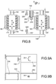
- FIGS. 9A and 9B respectively in plan view and in sectional view.
- an axis XX '201 is the sensitive axis of the sensor.
- References 202, 204, 206 respectively denote a seismic mass, a resonator, and a hinge. The sectional view shows that the mass 202 and the resonator 204 have the same thickness.
- the sensitive element 202 has a surface (in top view) of the order of mm 2 .
- a first approach is to postpone the MEMS on the MOS circuit once realized.
- the MEMS is in this case made by deposited layers.
- the metrological performances of the sensors thus produced are then quite limited, since the mechanical properties of the deposited materials are quite low compared to what is used when using the monocrystalline Si.
- the "In IC” approach consists in making the MEMS at the same level as the CMOS circuits. In this case, it is possible to have access to the Si monocrystalline to achieve the MEMS and thus obtain good performance.
- the homothetic miniaturization results in a "relative stiffening" of the mechanical structure with respect to the forces of inertia.
- the invention proposes making MEMS sensors with resonator detection using a "3D" planar technology.
- the invention relates to a resonant MEMS sensor in surface technology and excitation of the resonator in a plane, with multiple thicknesses. It is for example an accelerometer or a gyrometer. Typically one can have 2 different thicknesses on the same component, but also more than two thicknesses, for example three.
- a first thick zone has a first thickness and is used for the seismic mass part, for example an accelerometer or a gyrometer.
- a second zone, thin has a second thickness less than the first. The ratio between these two thicknesses is for example between 2 and 10. The second zone is used for the detection and possibly for the production of the hinges (or a torsion axis in the case of a gyroscope).
- the design of the resonant sensors made in surface technology is modified by decorrelating the seismic mass part of the detection part.
- the first zone preferably has a surface S less than 0.1 mm 2 for an accelerometer, and less than 5 mm 2 for a gyrometer.
- the first and second regions may be formed in the superficial semiconductor layer of an SOI substrate.
- a sensor according to the invention may further comprise a third hinge zone (or a torsion axis in the case of a gyrometer), this third zone having a thickness between that of the first zone and that of the second zone, or equal to that of the first zone, or equal to that of the second zone.
- Mechanical stops may be provided to limit the displacement of the seismic mass.
- Digital detection means may also be provided, for example comprising digital filtering means and / or digital signal processing.
- the invention also relates to a method for producing a device according to the invention, implementing differentiated etching steps, in depth, perpendicularly to a plane of the seismic mass, first and / or second and / or third areas.
- the thick zone and the thin zone may be formed by etching a layer of semiconductor material, in 3 dimensions.
- They can be formed by etching a superficial layer of semiconductor material of an SOI substrate in a direction (z) perpendicular to a main plane of this SOI substrate.
- Such a method may furthermore comprise the formation of a third zone, called the hinge zone or torsion axis, of thickness lying between that of the first zone and that of the second zone, or equal to one of the thicknesses of these zones. two areas.
- a third zone called the hinge zone or torsion axis
- the thin zone is formed in a semiconductor surface layer, the thick zone being made in an epitaxial semiconductor layer on said surface layer and in this superficial layer.
- Such a sensor 100 may be for example an accelerometer or a gyrometer. It's about of a sensor in surface technology and excitation of the resonator in a plane.
- an axis XX '1 is the sensitive axis of the sensor.
- References 2, 4 respectively denote a seismic mass, a resonator.
- the reference 6 designates a hinge in the case of an accelerometer and a torsion axis in the case of a gyrometer (a gyrometer is described below in connection with FIG. 8).
- the sectional view (FIG. 1B) shows that the mass 2 and the resonator 4 do not have the same thickness: the mass 2 has a first thickness E 1 , for example of the order of 1 ⁇ m, greater than the thickness E 2 of the resonator.
- the ratio E 1 / E 2 is for example between 2 and 10.
- the hinge makes it possible to maintain the seismic mass in the same plane, that of FIG. 1A or else that defined by the seismic mass 2, the dimensions of which in the plane of FIG. 1A are much larger than in a direction perpendicular to this plane.
- the hinge has a thickness E 3 which may be equal to E 1 , or E 2 , or between E 1 and E 2 .
- E 3 which may be equal to E 1 , or E 2 , or between E 1 and E 2 .
- the hinge 6 and the resonator 4 are made parallel to a plane defined by the seismic mass 2, but (FIG. 1B) at different depths in a direction z substantially perpendicular to the plane of the mass 2
- the hinge 6 is not necessarily parallel to the resonant portion 4; it may be arranged differently, for example as illustrated in FIG.
- FIGS. 1A and 1B designate identical elements or correspondents.
- the hinge is substantially perpendicular to the resonator. In the plane of the figures, arrangements other than those of FIGS. 1A-1B and 1C can be realized.
- Reference numeral 10 designates means for digital processing of a signal from the system 100. These means can be used in the embodiments illustrated in the other figures, although they are not represented.
- FIG. 1D are schematically represented, on the one hand, a structure 100 such as that described above, and on the other hand a second structure 200, of the same type, but in "head-to-tail” or differential mounting .
- an acceleration sensor according to the invention has a surface S (surface of the seismic mass 2, seen from above, or in the plane of FIG. 1A) less than 0.1 mm 2 or even 0, 05 mm 2 . In the case of a gyrometer, this upper value is preferably of the order of 5 mm 2 .
- a resonant sensor measures the natural frequency variation of a resonator (tuning fork type or vibrating beam) under the effect of an external constraint (inertia force in the present case).
- the the answer being a frequency
- a certain number of advantages related to the processing of electrical signals result from this, such as the possibility of being able to filter the signal (noise limitation) and to be able to process the information directly in digital mode by means 10 digital filtering and / or digital signal processing.
- the references 15, 15 'respectively denote an excitation electrode and a detection electrode.
- a measurement via a MOS can also be performed, the current of the channel being modulated by the displacement of the resonant structure which constitutes the gate of the transistor
- the significant increase of the sensitivity is equal to ⁇ f / f, where ⁇ f is the variation of resonance frequency under the effect of a mechanical stress induced by the displacement of the seismic mass or mass, a function of the acceleration, in the case of an accelerometer, or of a rotation speed in the case of a gyrometer.
- This increase can lead to a significant increase in the non-linearity of the sensor response as a function of the level of the acceleration (accelerometer case) or the speed of rotation (case of a gyrometer).
- We will therefore seek a good balance between the measuring range, the mass of the sensitive element 2 and the section of the resonator 4.
- the thinning of the mechanical zones results in a displacement of the force exerted by the seismic mass 2 on each zone.
- This thinning leads indeed to shift the center of gravity of the mass of the point of application of the force on the resonator (in z, that is to say according to the thickness, see Figure 1B).
- This offset can lead to a parasitic torque effect inducing for example a sensitivity to transverse accelerations.
- the thinning of the resonator also leads to a decrease in the excitation and / or detection capacity of the vibration.
- the electronics In order to limit the loss of electrical sensitivity it is possible to put the electronics to the nearest (possibly by an embodiment "In-IC" of the sensor) to limit the capacitances and / or parasitic resistances likely to degrade the signal / noise ratio.
- a resonant sensor In a resonant sensor according to the invention, the implementation of a "3D" planar technology (that is to say with etching in the plane of the mass 2, but also perpendicularly to this plane) makes it possible to decorrelate the detection part of the sensor (beam 4 or resonant tuning fork) of the inertial part (mass 2). This makes it possible to optimize these two elements separately in order to compensate for the decrease in sensitivity brought about by the miniaturization of the inertial sensors. This separate optimization is for example obtained during the production method, for example by separate engravings of the corresponding areas, as explained below.
- a decrease in the lateral dimensions of the beam 2 results in a gain in sensitivity.
- This decrease in lateral dimensions is nevertheless limited by the technology, that is to say by the resolution of the lithography and the aspect ratio of the engraving (the width of the pattern to be engraved is less than approximately 10 times the thickness to be engraved for a DRIE type equipment the decrease in the width of the resonator also tends to reduce its quality factor).
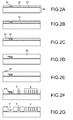
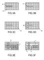
- FIGS. 2A - 2G and 3A - 3F A first method will be described in connection with FIGS. 2A - 2G and 3A - 3F.
- This first method uses a semiconductor epitaxy (here: Silicon, the SiGe is another example), which makes it possible to produce the resonant part in a first, low thickness, then the seismic mass and the hinge in a second thickness, epitaxial on the first thickness and greater than this first thickness.
- a semiconductor epitaxy here: Silicon, the SiGe is another example
- An SOI substrate 20 is first selected (Figure 2A). For example, it comprises a layer 22 of Si 1 ⁇ m thick for a layer 24 of SiO 2 oxide 0.4 ⁇ m thick.
- the etching is stopped on the layer 24 of SiO 2 .
- a layer (not shown) of SiO 2 for example of thickness 2 ⁇ m, is then deposited, followed by a planarization with a stop on layer 22 of Si, then with a deposit 32 of SiO 2 , for example about 0.4 ⁇ m thick ( Figure 2B).
- FIGS. 2C and 3B lithography by etching, in layer 32 of SiO 2 , of a protection 34 above the resonator, with overflow at the level of the excitation / detection electrode.
- Silicon epitaxy 35 is then carried out (FIGS. 2D and 3C) on the initial semiconductor surface layer 22, for example to a thickness of approximately 3 ⁇ m, greater than the thickness of layer 32.
- the device is finally released by HF etching (wet or vapor) of the layer 24 (FIGS. 2G and 3F).
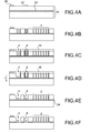
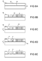
- a second method according to the invention implements a thinning of the resonator 4 and the hinge 6 by etching (FIGS. 4A-4F and 5A-5E).
- An SOI substrate 20 is first selected ( Figure 4A). For example, it comprises a layer 22 of Si of 4 microns thickness for oxide layer 24 of SiO 2 of 0.4 .mu.m thick.
- a Ti / Ni / Au metal deposit and a litho-etching are then made to form contacts 36 (FIGS. 4A and 5A).
- lithography is carried out (FIGS. 4C and 5C), which makes it possible to open the resonator 4, with overflow at the excitation electrode / detection and opening on the hinge 6.
- the device is released by HF etching (wet or vapor) of the layer 24 (FIGS. 4F and 5E).
- the hinge and resonant zones have identical thicknesses because they are etched in depth, along the z axis, during the same step, whereas the patterns of the seismic mass zone are not engraved in this direction.
- a third method according to the invention is a variant of the second embodiment, with, in addition, a differential thinning of the resonator 4 and the hinge 6 (or of another mechanical part).
- a SOI substrate 20 is first of all selected ( Figure 6A). For example, it comprises a layer 22 of Si of 4 microns thickness for oxide layer 24 of SiO 2 of 0.4 .mu.m thick.
- a Ti / Ni / Au metal deposit and a litho-etching are then made to form contacts 36 (FIGS. 6A and 7A).
- This step therefore makes it possible to etch the patterns of the seismic mass zone, the resonator zone and the hinge zone.
- the patterns of these last two zones will then be able to be engraved in depth, along the z axis (FIGS. 6C and 6D), but separately to be able to control their relative final thickness.
- an opening of the resonator is produced by lithography, with overflow at the level of the excitation / detection electrode.
- the resonator is etched (RIE or DRIE) along the z axis and then removed from the resin 35.
- FIG. 6D after another deposit of resin 37, a lithographic opening is made at the hinge 6.
- a DRIE etching is carried out along the z axis, but of the hinge 6, then at a removal of the resin 37.
- the device is released by HF etching (wet or vapor) of the layer 24 (FIGS. 6E and 7E).
- the hinge and resonant zones have different thicknesses from one another, and different from the thickness of the seismic zone, because they are etched in depth, along the z axis, during different stages, while the grounds of the seismic mass zone are not etched in this direction.
- the first embodiment although a little more complex (it implements additional steps of planarization and epitaxy), makes it possible to optimize the electrical sensitivity of the electromechanical resonator (optimization of the signal / noise ratio by increasing the capacitances helpful).
- the air gap between the resonator and the excitation / detection electrodes is made directly in a very thin part of silicon. Since the etching of the air gap is done with a thin thickness, a high machining resolution can be achieved.
- resonators and gaps are made on a thick silicon, limiting the fineness of the machining, before being thinned.
- the invention uses zones of different thicknesses in a sensor.
- a sensor according to the invention can be produced by machining silicon or a semiconductor material in the 3 dimensions.
- a resonator according to the invention obtained by 3D machining in a semiconductor material, is particularly well suited for a resonator detection gyro.
- the principle of such a gyrometer is indicated in the document FR-2,874,257 , which is also shown diagrammatically in FIG. 8. It comprises a support, not shown, and two seismic masses 120, 120 'which are movable in the plane (X, Y) of the support, and in particular which can vibrate. These two masses are coupled by connecting means, also moving relative to the support.
- two link arms 140, 140 ' here parallel, are connected to the moving masses via means 160, 160' having sufficient flexibility to allow the relative movements of the two masses 120, 120 'relative to each other.
- the link arms 140, 140 'and the flexible means, or bending arm, 160, 160' form a rectangular frame; the flexible means 160, 160 'may for example be bending springs or an attachment tongue.
- Means are provided to put the masses 120, 120 'in vibration in the plane (X, Y) of the support, for example excitation combs 180, 180' interlocking in one or both sides of each mobile mass 120 , 120 '.
- the masses 120, 120 ' are excited, preferably at resonance or in the vicinity of the resonance, by means of electrostatic forces applied via the inter-digit comb structures 180, 180' together.
- masses 120, 120 'and connecting means 140, 140', 160, 160 'thus form a first resonator
- the resonance operation makes it possible to obtain a high amplitude of displacement, and a large quality factor, thereby increasing the sensitivity of the gyrometer.
- the vibration of the masses 120, 120 ' is in phase opposition, that is to say that their movements are in the opposite direction at each instant: the distance separating the two masses 120, 120' is variable, this variation being tolerated by the flexible means 160, 160 '. This allows detection by second resonators.
- the rotational speed ⁇ about the Z axis is then deduced from the measured frequency displacement.
- the resonator 220 is excited and controlled preferably on its resonance peak or in its vicinity; a digital electronic system makes it possible to easily go back to the resonant frequency at any moment.
- the resonator 220 may for example be in the form of a vibrating beam as shown diagrammatically in FIG. 8, one end of which is connected to the connecting arm 140 and the other end is anchored to the substrate by any known means 240.
- the resonator 220 is excited capacitively resonance by fixed electrodes which are also used for detection. It is also possible to have a detection electrode 260 that is dissociated from the excitation electrode 280.
- Electromagnetic excitation is also possible, as can detection by piezoelectric gage.
- each arm 140, 140 ' is located a torsion axis 300, 300' intended to transform the forces of Coriolis acting at the masses 120, 120 in a pair of forces around this torsion axis 300, 300 ', by a lever effect which makes it possible to exert the greatest possible stress on the resonator.
- Each of the torsion axes is thus attached at one end to the support by an anchor 320, 320 'and at the other end to the connecting arm 140, 140', 160, 160 ', towards the center of the structure 200 to limit the temperature drifts of the gyrometer.
- FIGS. 4A-4D of the document FR-2874257 for example two resonators on one and the same link arm 140 (FIG. 4A), or located on the same side of an axis of the mobile device defined by the torsion axes (FIG. 4B), or else with tuning fork type resonators (FIG. FIG. 4C), or again with resonators arranged as in FIG. 4D of this same document.
- FIGS. 4A-4D of the document FR-2874257 for example two resonators on one and the same link arm 140 (FIG. 4A), or located on the same side of an axis of the mobile device defined by the torsion axes (FIG. 4B), or else with tuning fork type resonators (FIG. FIG. 4C), or again with resonators arranged as in FIG. 4D of this same document.
- the invention makes it possible to produce one or more resonators with a thickness or section smaller than that of the seismic mass or masses.
- the invention makes it possible to have inertial sensors (accelerometers or gyrometers) of very good performance (sensitivity) for very small dimensions.
Landscapes
- Physics & Mathematics (AREA)
- General Physics & Mathematics (AREA)
- Engineering & Computer Science (AREA)
- Radar, Positioning & Navigation (AREA)
- Remote Sensing (AREA)
- Manufacturing & Machinery (AREA)
- Gyroscopes (AREA)
- Pressure Sensors (AREA)
- Micromachines (AREA)
- Diaphragms For Electromechanical Transducers (AREA)
Abstract
Description
L'invention concerne le domaine des micro-capteurs, notamment en silicium, par exemple les capteurs inertiels, notamment accéléromètres ou gyromètres.The invention relates to the field of micro-sensors, in particular silicon, for example inertial sensors, including accelerometers or gyrometers.
Elle trouve application dans des domaines variés, tels que l'automobile, la téléphonie mobile ou l'avionique.It finds application in various fields, such as automotive, mobile telephony or avionics.
De manière connue, les capteurs résonants peuvent être réalisés :
- Soit en technologie de volume, auquel cas l'élément sensible du capteur est réalisé sur toute l'épaisseur d'un substrat en silicium ou en quartz, en utilisant des gravures humides ; une telle technique est décrite dans le
document FR 2 763 694 - Soit en technologie de surface : cette technique est décrite dans le document
« Resonant accelerometer with self test », de M.Aikele et al., Sensors and Actuators, A92, 2001, p. 161-167
- Either in volume technology, in which case the sensing element of the sensor is made over the entire thickness of a silicon or quartz substrate, using wet etchings; such a technique is described in the
document FR 2 763 694 - Or in surface technology: this technique is described in the document
"Resonant accelerometer with self test", by M.Aikele et al., Sensors and Actuators, A92, 2001, p. 161-167
Les capteurs inertiels réalisés en technologie de volume sont basés sur une excitation électrostatique hors plan du résonateur. De ce fait ils nécessitent le report de 2 substrats, dont l'un sert à réaliser la (ou les) électrode(s) d'excitation/détection et le second sert à fermer la cavité sous vide. Les technologies mises en jeu sont donc lourdes.Inertial sensors made in volume technology are based on off-plane electrostatic excitation of the resonator. As a result, they require the transfer of 2 substrates, one of which serves to produce the excitation / detection electrode (s) and the second serves to close the vacuum cavity. The technologies involved are therefore heavy.
De plus le résonateur a alors une épaisseur différente de la masse sismique. Cet amincissement est, entre autre, rendu nécessaire par le mode de vibration de la poutre qui se fait hors plan.In addition, the resonator then has a thickness different from the seismic mass. This thinning is, among other things, made necessary by the vibration mode of the beam which is off plan.
Un autre problème de ce type de technique réside dans le positionnement du résonateur, qui ne peut pas être optimisé pour augmenter l'effet de bras de levier. En effet, afin de minimiser l'entrefer entre le résonateur et son électrode d'excitation, le résonateur est placé en surface du substrat. De manière optimum, le résonateur devrait se situer le plus près possible de la charnière (axe de rotation de la masse).Another problem with this type of technique is the positioning of the resonator, which can not be optimized to increase the leverage effect. Indeed, in order to minimize the gap between the resonator and its excitation electrode, the resonator is placed on the surface of the substrate. Optimally, the resonator should be as close as possible to the hinge (axis of rotation of the mass).
Dans un capteur inertiel réalisé en technologie de surface le résonateur vibre dans un plan. Le principe d'un capteur inertiel selon l'art antérieur est illustré sur les figures 9A et 9B, respectivement en vue de dessus et en vue en coupe.In an inertial sensor realized in surface technology the resonator vibrates in a plane. The principle of an inertial sensor according to the prior art is illustrated in FIGS. 9A and 9B, respectively in plan view and in sectional view.
Sur ces figures, un axe XX' 201 est l'axe sensible du capteur. Les références 202, 204, 206 désignent respectivement une masse sismique, un résonateur, et une charnière. La vue en coupe montre que la masse 202 et le résonateur 204 ont une même épaisseur.In these figures, an axis XX '201 is the sensitive axis of the sensor.
L'élément sensible 202 a une surface (en vue de dessus) de l'ordre du mm2.The
Or, dans de multiples applications, et notamment des applications grand public comme l'automobile ou la téléphonie mobile, où la demande en capteurs est croissante, la miniaturisation des composants reste un enjeu important, du fait en particulier de la course à la réduction du prix, à l'accroissement des fonctionnalités (nombre de capteurs de plus en plus important), à l'intégration avec l'électronique de traitement et à la réduction de la consommation.However, in many applications, including consumer applications such as automotive or mobile telephony, where the demand for sensors is increasing, the miniaturization of components remains an important issue, in particular because of the race for price reduction, the increase in functionalities (a growing number of sensors), the integration with electronic processing and the reduction of consumption.
Il faut donc trouver une nouvelle conception de composants, encore plus miniaturisés, de masse encore plus faible que ceux connus actuellement, présentant un encombrement, pour les accéléromètres, de préférence inférieur à 0,1 mm2 ou même à 0,01 mm2.It is therefore necessary to find a new design of components, even more miniaturized, even smaller mass than those currently known, having a footprint, for accelerometers, preferably less than 0.1 mm 2 or even 0.01 mm 2 .
De même, toujours aux fins de miniaturisation, on cherche à associer électronique et MEMS et/ou NEMS sur un même substrat. Pour cette association, deux options existent.In the same way, always for the purpose of miniaturization, one seeks to associate electronics and MEMS and / or NEMS on the same substrate. For this association, two options exist.
Une première approche, dite « Above IC» (ou AIC), consiste à reporter le MEMS sur le circuit MOS une fois réalisé. Le MEMS est dans ce cas réalisé par couches déposées. Les performances métrologiques des capteurs ainsi réalisés sont alors assez limitées, puisque les qualités mécaniques des matériaux déposés sont assez faibles au regard de ce que l'on a en utilisant le Si monocristallin.A first approach, called "Above IC" (or AIC), is to postpone the MEMS on the MOS circuit once realized. The MEMS is in this case made by deposited layers. The metrological performances of the sensors thus produced are then quite limited, since the mechanical properties of the deposited materials are quite low compared to what is used when using the monocrystalline Si.
L'approche « In IC » consiste à réaliser le MEMS au même niveau que les circuits CMOS. Dans ce cas, il est possible d'avoir accès au Si monocristallin pour réaliser le MEMS et ainsi obtenir de bonnes performances.The "In IC" approach consists in making the MEMS at the same level as the CMOS circuits. In this case, it is possible to have access to the Si monocrystalline to achieve the MEMS and thus obtain good performance.
Pour des capteurs de classe 10-2 (et au-delà), il parait illusoire d'obtenir le niveau de performance requis par une technologie AIC dans les dimensions visées. L'approche « In-IC » apparaît à ce titre beaucoup plus prometteuse. Cette approche n'a cependant de sens que si l'on dispose d'une miniaturisation suffisamment poussée des structures mécaniques. En effet, pour rendre cette intégration réaliste d'un point de vue économique il convient de minimiser au maximum la surface de silicium occupée par le capteur au profit des circuits CMOS. On estime à environ 0.05mm2 l'encombrement maximum à ne pas dépasser pour un accéléromètre de ce type. A titre de comparaison, la surface classique de l'élément sensible d'un accéléromètre MEMS (de classe 10-2 ou de gamme de mesure 10G) descend rarement en dessous de 0.5mm2 (sans tenir compte des plots de contact). Pour un gyroscope MEMS, la surface usuelle de l'élément sensible est de plus de 20 mm2.For
D'une manière générale, quel que soit le type de capteur inertiel, la miniaturisation par simple réduction homothétique des dimensions se traduit inexorablement par une perte de sensibilité significative. C'est ce qu'indique l'article de
Autrement dit, la miniaturisation homothétique se traduit par une « rigidification relative » de la structure mécanique par rapport aux forces d'inertie.In other words, the homothetic miniaturization results in a "relative stiffening" of the mechanical structure with respect to the forces of inertia.
Il se pose donc, outre le problème de trouver une nouvelle conception de composants, encore plus miniaturisés, celui de devoir pallier cette baisse significative de sensibilité qui accompagne toute réduction de la taille des composants.It raises therefore, in addition to the problem of finding a new design of components, even more miniaturized, that of having to mitigate this decline significant sensitivity that accompanies any reduction in the size of the components.
Pour résoudre ces problèmes, l'invention propose de réaliser des capteurs MEMS à détection par résonateur utilisant une technologie planaire « 3D ».To solve these problems, the invention proposes making MEMS sensors with resonator detection using a "3D" planar technology.
L'invention concerne un capteur résonant MEMS en technologie de surface et à excitation du résonateur dans un plan, à épaisseurs multiples. C'est par exemple un accéléromètre ou un gyromètre. Typiquement on peut avoir 2 épaisseurs différentes sur le même composant, mais aussi plus de deux épaisseurs, par exemple trois.The invention relates to a resonant MEMS sensor in surface technology and excitation of the resonator in a plane, with multiple thicknesses. It is for example an accelerometer or a gyrometer. Typically one can have 2 different thicknesses on the same component, but also more than two thicknesses, for example three.
Une première zone épaisse, présente une première épaisseur, et est utilisée pour la partie masse sismique, par exemple d'un accéléromètre ou d'un gyromètre. Une seconde zone, mince, a une deuxième épaisseur inférieure à la première. Le rapport entre ces deux épaisseurs est par exemple compris entre 2 et 10. La seconde zone est utilisée pour la détection et éventuellement pour la réalisation des charnières (ou d'un axe de torsion dans le cas d'un gyroscope).A first thick zone has a first thickness and is used for the seismic mass part, for example an accelerometer or a gyrometer. A second zone, thin, has a second thickness less than the first. The ratio between these two thicknesses is for example between 2 and 10. The second zone is used for the detection and possibly for the production of the hinges (or a torsion axis in the case of a gyroscope).
Selon l'invention, on modifie le design des capteurs résonants réalisés en technologie de surface en décorrélant la partie masse sismique de la partie détection.According to the invention, the design of the resonant sensors made in surface technology is modified by decorrelating the seismic mass part of the detection part.
La première zone présente de préférence une surface S inférieure à 0,1 mm2 pour un accéléromètre, et inférieure à 5 mm2 pour un gyromètre.The first zone preferably has a surface S less than 0.1 mm 2 for an accelerometer, and less than 5 mm 2 for a gyrometer.
La première et la deuxième zone peuvent être formées dans la couche superficielle de semi-conducteur d'un substrat SOI.The first and second regions may be formed in the superficial semiconductor layer of an SOI substrate.
Un capteur selon l'invention peut en outre comporter une troisième zone formant charnière (ou un axe de torsion dans le cas d'un gyromètre), cette troisième zone ayant une épaisseur comprise entre celle de la première zone et celle de la deuxième zone, ou égale à celle de la première zone, ou égale à celle de la deuxième zone.A sensor according to the invention may further comprise a third hinge zone (or a torsion axis in the case of a gyrometer), this third zone having a thickness between that of the first zone and that of the second zone, or equal to that of the first zone, or equal to that of the second zone.
L'invention permet d'optimiser différentes parties du capteur séparément:
- le (les) résonateur(s),
- la (les) charnière(s), ou l'axe de torsion,
- la (les) masse(s) sismique(s).
- the resonator (s),
- the hinge (s), or the torsion axis,
- the seismic mass (es).
Elle est en outre compatible avec une approche « In-IC » à très bas coût.It is also compatible with an "In-IC" approach at very low cost.
Des butées mécaniques peuvent être prévues, afin de limiter le déplacement de la masse sismique.Mechanical stops may be provided to limit the displacement of the seismic mass.
Des moyens numériques de détection peuvent en outre être prévus, par exemple comportant des moyens de filtrage numérique et/ou de traitement numérique du signal.Digital detection means may also be provided, for example comprising digital filtering means and / or digital signal processing.
L'invention concerne en outre un procédé de réalisation d'un dispositif selon l'invention, mettant en oeuvre des étapes de gravure différenciées, en profondeur, perpendiculairement à un plan de la masse sismique, des première et/ou deuxième et/ou troisièmes zones.The invention also relates to a method for producing a device according to the invention, implementing differentiated etching steps, in depth, perpendicularly to a plane of the seismic mass, first and / or second and / or third areas.
L'invention concerne en particulier un procédé de réalisation d'un capteur résonant MEMS, du type de surface, comportant un résonateur à excitation dans le plan, ce procédé comportant :
- la formation d'une zone épaisse, présentant une première épaisseur (E1), formant masse sismique,
- la formation d'une zone mince, présentant une deuxième épaisseur (E2), inférieure à la première, pour la détection.
- the formation of a thick zone, having a first thickness (E 1 ) forming a seismic mass,
- forming a thin zone, having a second thickness (E 2 ), less than the first, for the detection.
La zone épaisse et la zone mince peuvent être formées par gravure d'une couche de matériau semi-conducteur, suivant 3 dimensions.The thick zone and the thin zone may be formed by etching a layer of semiconductor material, in 3 dimensions.
Elles peuvent être formée par gravure d'une couche superficielle de matériau semi-conducteur d'un substrat SOI, suivant une direction (z) perpendiculaire à un plan principal de ce substrat SOI.They can be formed by etching a superficial layer of semiconductor material of an SOI substrate in a direction (z) perpendicular to a main plane of this SOI substrate.
Un tel procédé peut en outre comporter la formation d'une troisième zone, dite zone charnière ou axe de torsion, d'épaisseur comprise entre celle de la première zone et celle de la deuxième zone, ou égale à l'une des épaisseurs de ces deux zones.Such a method may furthermore comprise the formation of a third zone, called the hinge zone or torsion axis, of thickness lying between that of the first zone and that of the second zone, or equal to one of the thicknesses of these zones. two areas.
Avantageusement, la zone mince est réalisée dans une couche superficielle de semi-conducteur, la zone épaisse étant réalisée dans une couche de semi-conducteur épitaxiée sur ladite couche superficielle et dans cette couche superficielle.Advantageously, the thin zone is formed in a semiconductor surface layer, the thick zone being made in an epitaxial semiconductor layer on said surface layer and in this superficial layer.
- Les figures 1A et 1B représentent, respectivement en vue de dessus et en vue de côté, un capteur inertiel selon l'invention.Figures 1A and 1B show, respectively in top view and in side view, an inertial sensor according to the invention.
- La figure 1C représente, en vue de dessus, un capteur inertiel selon l'invention avec une autre disposition des éléments dans un plan.FIG. 1C represents, in top view, an inertial sensor according to the invention with another arrangement of the elements in a plane.
- La figure 1D représente, en vue de dessus, un dispositif selon l'invention, avec deux capteurs inertiels selon l'invention montés en différentiel.FIG. 1D represents, in a view from above, a device according to the invention, with two inertial sensors according to the invention mounted in differential.
- Les figures 2A - 2G et 3A - 3F représentent un premier mode de réalisation d'un procédé selon l'invention,FIGS. 2A-2G and 3A-3F represent a first embodiment of a method according to the invention,
- Les figures 4A - 4F et 5A - 5E représentent un deuxième mode de réalisation d'un procédé selon l'invention.FIGS. 4A-4F and 5A-5E show a second embodiment of a method according to the invention.
- Les figures 6A - 6E et 7A - 7E représentent un troisième mode de réalisation d'un procédé selon l'invention.Figures 6A-6E and 7A-7E show a third embodiment of a method according to the invention.
- La figure 8 représente un gyromètre.Figure 8 shows a gyrometer.
- Les figures 9A et 9B représentent, respectivement en vue de dessus et en vue de côté, un capteur inertiel selon l'art antérieur.Figures 9A and 9B show, respectively in top view and in side view, an inertial sensor according to the prior art.
Un exemple de capteur inertiel résonant 100 selon l'invention va être décrit en liaison avec les figures 1A et 1B. Un tel capteur 100 peut être par exemple un accéléromètre ou un gyromètre. Il s'agit d'un capteur en technologie de surface et à excitation du résonateur dans un plan.An example of a resonant
Sur ces figures, un axe XX' 1 est l'axe sensible du capteur. Les références 2, 4 désignent respectivement une masse sismique, un résonateur. La référence 6 désigne une charnière dans le cas d'un accéléromètre et un axe de torsion dans le cas d'un gyromètre (un gyromètre est décrit plus loin en liaison avec la figure 8). La vue en coupe (figure 1B) montre que la masse 2 et le résonateur 4 n'ont pas la même épaisseur : la masse 2 a une première épaisseur E1, par exemple de l'ordre du µm, supérieure à l'épaisseur E2 du résonateur. Le rapport E1/E2 est par exemple compris entre 2 et 10.In these figures, an axis XX '1 is the sensitive axis of the sensor.
La charnière permet de maintenir la masse sismique dans un même plan, celui de la figure 1A ou encore celui défini par la masse sismique 2 dont les dimensions dans le plan de la figure 1A sont nettement plus importantes que dans une direction perpendiculaire à ce plan. La charnière a une épaisseur E3 qui peut être égale à E1, ou à E2, ou comprise entre E1 et E2. Comme on le voit sur la figure 1A, la charnière 6 et le résonateur 4 sont réalisés parallèlement à un plan défini par la masse sismique 2, mais (figure 1B) à des profondeurs différentes suivant une direction z sensiblement perpendiculaire au plan de la masse 2. La charnière 6 n'est pas nécessairement parallèle à la portion résonante 4 ; elle peut être disposée autrement, par exemple comme illustré sur la figure 1C sur laquelle des références identiques à celles des figures 1A et 1B désignent des éléments identiques ou correspondants. Sur cette figure 1C, qui représente un dispositif selon l'invention en vue de dessus, la charnière est sensiblement perpendiculaire au résonateur. Dans le plan des figures, des dispositions autres que celles des figures 1A-1B et 1C peuvent être réalisées.The hinge makes it possible to maintain the seismic mass in the same plane, that of FIG. 1A or else that defined by the
La référence 10 (figure 1A) désigne des moyens de traitement numérique d'un signal provenant du système 100. Ces moyens peuvent être utilisés dans les modes de réalisation illustrés sur les autres figures, bien qu'ils n'y soient pas représentés.Reference numeral 10 (FIG. 1A) designates means for digital processing of a signal from the
L'invention s'applique également à une structure différentielle, c'est-à-dire à une structure dans laquelle des capteurs sont montés en différentiel. Ainsi, sur la figure 1D, sont représentées schématiquement, d'une part une structure 100 telle que celle décrite ci-dessus, et d'autre part une deuxième structure 200, de même type, mais en montage « tête bêche », ou différentiel.The invention also applies to a differential structure, that is to say to a structure in which sensors are mounted in differential. Thus, in FIG. 1D, are schematically represented, on the one hand, a
La mesure par résonateur est bien adaptée à une miniaturisation des dimensions. Par exemple, un capteur d'accélération selon l'invention présente une surface S (surface de la masse sismique 2, en vue de dessus, ou dans le plan de la figure 1A) inférieure à 0,1 mm2 ou même à 0,05 mm2. Dans le cas d'un gyromètre, cette valeur supérieure est de préférence de l'ordre de 5 mm2.The resonator measurement is well adapted to a miniaturization of the dimensions. For example, an acceleration sensor according to the invention has a surface S (surface of the
Un capteur résonant mesure la variation de fréquence propre d'un résonateur (type diapason ou poutre vibrante) sous l'effet d'une contrainte extérieure (force d'inertie dans le cas présent). La réponse exploitée étant une fréquence, un certain nombre d'avantages, liés au traitement des signaux électriques, en découlent, comme la possibilité de pouvoir filtrer le signal (limitation du bruit) et de pouvoir traiter l'information directement en numérique par des moyens 10 de filtrage numérique et/ou de traitement numérique du signal. En fait c'est une mesure d'une fréquence de vibration par le biais d'une mesure capacitive (i = d (CV) /dt = CdV/dt + V dC/dt, la quantité mesurée étant V dC/dt). Sur la figure 1A , les références 15, 15' désignent respectivement une électrode d'excitation et une électrode de détection. Une mesure via un MOS peut aussi être réalisée, le courant du canal étant modulé par le déplacement de la structure résonante qui constitue la grille du transistor.A resonant sensor measures the natural frequency variation of a resonator (tuning fork type or vibrating beam) under the effect of an external constraint (inertia force in the present case). The the answer being a frequency, a certain number of advantages related to the processing of electrical signals result from this, such as the possibility of being able to filter the signal (noise limitation) and to be able to process the information directly in digital mode by means 10 digital filtering and / or digital signal processing. In fact it is a measure of a frequency of vibration by means of a capacitive measurement (i = d (CV) / dt = CdV / dt + V dC / dt, the measured quantity being V dC / dt). In FIG. 1A, the
Ce principe de mesure résonante permet également :
- De travailler à la résonance mécanique, c'est-à-dire avec des amplitudes de déflexion du corps vibrant 2 optimisées, et ainsi de permettre une détection capacitive plus propre.
- D'avoir une précision de mesure faiblement dépendante du bruit électrique lié à la variation de capacité.
- To work on mechanical resonance, that is to say with amplitudes of deflection of the vibrating
body 2 optimized, and thus to allow a cleaner capacitive detection. - To have a measurement accuracy that is slightly dependent on the electrical noise related to the variation of capacity.
En terme de dimensionnement, le fait de réduire notablement la section du résonateur n'est pas sans conséquence.In terms of dimensioning, significantly reducing the section of the resonator is not inconsequential.
L'augmentation importante de la sensibilité est égale à Δf/f, où Δf est la variation de fréquence de résonance sous l'effet d'une contrainte mécanique induite par le déplacement de la ou des masse sismique, fonction de l'accélération, dans le cas d'un accéléromètre, ou d'une vitesse de rotation dans le cas d'un gyromètre. Cette augmentation peut conduire à une augmentation notable de la non linéarité de réponse du capteur en fonction du niveau de l'accélération (cas de l'accéléromètre) ou de la vitesse de rotation (cas d'un gyromètre). On recherchera donc un bon équilibre entre la gamme de mesure, la masse de l'élément sensible 2 et la section du résonateur 4.The significant increase of the sensitivity is equal to Δf / f, where Δf is the variation of resonance frequency under the effect of a mechanical stress induced by the displacement of the seismic mass or mass, a function of the acceleration, in the case of an accelerometer, or of a rotation speed in the case of a gyrometer. This increase can lead to a significant increase in the non-linearity of the sensor response as a function of the level of the acceleration (accelerometer case) or the speed of rotation (case of a gyrometer). We will therefore seek a good balance between the measuring range, the mass of the
La diminution de section des différents éléments mécaniques dans les zones amincies peut conduire à une concentration importante des contraintes. Ces contraintes peuvent être analysées pour éviter le flambage et la rupture de ces éléments, sous l'effet d'un choc par exemple. Pour résoudre ou limiter ce problème, il est possible d'ajouter des butées mécaniques limitant le déplacement de la masse. De telles butées 12 sont représentées sur la figure 1B.The reduction in section of the different mechanical elements in the thinned zones can lead to a high concentration of the stresses. These constraints can be analyzed to avoid buckling and breaking of these elements, under the effect of a shock for example. To solve or limit this problem, it is possible to add mechanical stops limiting the movement of the mass. Such stops 12 are shown in FIG. 1B.
L'amincissement des zones mécaniques résulte en un déplacement de l'effort exercé par la masse sismique 2 sur chaque zone. Cet amincissement conduit en effet à décaler le centre de gravité de la masse du point d'application de la force sur le résonateur (en z, c'est à dire suivant l'épaisseur, voir figure 1B). Ce décalage peut conduire à un effet de couple parasite induisant par exemple une sensibilité aux accélérations transverses.The thinning of the mechanical zones results in a displacement of the force exerted by the
L'amincissement du résonateur conduit à diminuer également la capacité d'excitation et/ou de détection de la vibration. Afin de limiter la perte de sensibilité électrique il est possible de mettre l'électronique au plus proche (éventuellement par une réalisation « In-IC » du capteur) pour limiter les capacités et/ou résistances parasites susceptibles de dégrader le rapport Signal/Bruit.The thinning of the resonator also leads to a decrease in the excitation and / or detection capacity of the vibration. In order to limit the loss of electrical sensitivity it is possible to put the electronics to the nearest (possibly by an embodiment "In-IC" of the sensor) to limit the capacitances and / or parasitic resistances likely to degrade the signal / noise ratio.
Pour dimensionner un dispositif selon l'invention, on peut utiliser un logiciel de type « éléments finis » comme ANSYS ou Coventor ou tout autre logiciel d'aide à la conception comme FEMLab ou Matlab.In order to size a device according to the invention, it is possible to use a "finite element" type software such as ANSYS or Coventor or any other design assistance software such as FEMLab or Matlab.
Dans un capteur résonant selon l'invention, la mise en oeuvre d'une technologie planaire « 3D » (c'est-à-dire avec gravure dans le plan de la masse 2, mais aussi perpendiculairement à ce plan) permet de décorréler la partie détection du capteur (poutre 4 ou diapason résonant) de la partie inertielle (masse 2). Ceci permet d'optimiser séparément ces deux éléments pour palier la diminution de sensibilité amenée par la miniaturisation des capteurs inertiels. Cette optimisation séparée est par exemple obtenue lors du procédé de réalisation, par exemple par gravures séparées des zones correspondantes, comme expliqué plus loin.In a resonant sensor according to the invention, the implementation of a "3D" planar technology (that is to say with etching in the plane of the
En effet la force d'inertie qui s'applique sur le résonateur est directement proportionnelle au volume de la masse sismique mise en jeu. Donc toute réduction de dimension résulte en une diminution de cette force et donc en une perte de sensibilité.Indeed the inertial force that applies to the resonator is directly proportional to the volume of the seismic mass involved. So any reduction in size results in a decrease in this force and therefore in a loss of sensitivity.
Dans le cas du résonateur de détection, la réduction de certaines dimensions (sections) du résonateur conduit à une augmentation de sensibilité, c'est-à-dire à une variation de fréquence de résonance plus importante pour une contrainte donnée. En d'autres termes, plus la section du résonateur est petite, plus la fréquence de résonance du résonateur varie en fonction de la contrainte qui y est appliquée. Pour une force extérieure donnée s'exerçant sur le résonateur, la variation de sa fréquence f de résonance sera d'autant plus importante que la section du résonateur 4 sera faible : 
avec :
- f : fréquence propre du résonateur sur lequel s'exerce la contrainte axiale Fi;
- f0 : la fréquence centrale sans effort (Fi = 0),
- Fi : la force d'inertie appliquée sur la poutre 4,
- L, t et 1 : respectivement la longueur, l'épaisseur et la largeur de la poutre 4,
- E: le module d'Young.
- Δf = fFi≠0 - f0 ; Δf/f0 est la susceptibilité du capteur, et augmente lorsque la section du résonateur diminue.
with:
- f: eigenfrequency of the resonator on which the axial stress F i is exerted;
- f 0 : the central frequency without effort (F i = 0),
- F i : the inertial force applied to the
beam 4, - L, t and 1: respectively the length, the thickness and the width of the
beam 4, - E: the Young's modulus.
- Δf = f Fi ≠ 0 - f 0 ; Δf / f 0 is the susceptibility of the sensor, and increases when the section of the resonator decreases.
On cherche à réduire le terme tl3 pour accroître le rapport Δf/f.We seek to reduce the term tl 3 to increase the ratio Δf / f.
Une diminution des dimensions latérales de la poutre 2 se traduit par un gain en sensibilité. Cette diminution des dimensions latérales est néanmoins limitée par la technologie, c'est-à-dire par la résolution de la lithographie et le rapport de forme de la gravure (la largeur du motif à graver est inférieure à environ 10 fois l'épaisseur à graver pour un équipement de type DRIE ; la diminution de la largeur du résonateur tend également à faire chuter son facteur de qualité).A decrease in the lateral dimensions of the
Pour aller encore plus loin dans la réduction de section du résonateur, on peut amincir le résonateur 2, sans toucher à la masse sismique 4 et aux zones d'ancrages ; il peut en effet être avantageux d'amincir d'autres parties mobiles du capteur comme les charnières 6, dans le cas d'un accéléromètre, ou l'axe de torsion dans le cas d'un gyromètre. Cela revient à utiliser une technologie de surface (ou technologie planaire) « 3D », ou une méthode selon l'invention, dans laquelle on amincit sélectivement certaines parties du MEMS.To go further in reducing the section of the resonator, it is possible to thin the
Trois exemples de réalisations d'un dispositif selon l'invention sont présentés ci-dessous. Ces trois exemples peuvent en outre être combinés entre eux. Ils sont décrits dans le cas d'un accéléromètre. Dans le cas d'un gyromètre, on remplace le terme « charnière » par l'expression « axe de torsion ».Three examples of embodiments of a device according to the invention are presented below. These three examples can further be combined with each other. They are described in the case of an accelerometer. In the case of a gyrometer, the term "hinge" is replaced by the expression "torsion axis".
Un premier procédé va être décrit en liaison avec les figures 2A - 2G et 3A - 3F.A first method will be described in connection with FIGS. 2A - 2G and 3A - 3F.
Ce premier procédé met en oeuvre une épitaxie de semi-conducteur (ici : Silicium ; le SiGe est un autre exemple), ce qui permet de réaliser la partie résonante dans une première épaisseur, faible, puis la masse sismique et la charnière dans une deuxième épaisseur, épitaxiée sur la première épaisseur et plus importante que cette première épaisseur.This first method uses a semiconductor epitaxy (here: Silicon, the SiGe is another example), which makes it possible to produce the resonant part in a first, low thickness, then the seismic mass and the hinge in a second thickness, epitaxial on the first thickness and greater than this first thickness.
Un substrat SOI 20 est tout d'abord sélectionné (figure 2A). Par exemple, il comporte une couche 22 de Si de 1 µm d'épaisseur pour une couche 24 d'oxyde SiO2 de 0.4 µm d'épaisseur.An
Il est ensuite procédé à une lithographie puis une gravure de la couche 22 de Si pour définir l'entrefer 30 du résonateur (figures 2A et 3A). Cet entrefer est donc défini dans la couche superficielle de semi-conducteur, d'épaisseur faible.It is then proceeded with a lithography and etching of the
La gravure est arrêtée sur la couche 24 de SiO2. On procède ensuite au dépôt d'une couche (non représentée) de SiO2, par exemple d'épaisseur 2 µm, suivi d'une planarisation avec arrêt sur la couche 22 de Si, puis à un dépôt 32 de SiO2, par exemple d'environ 0.4 µm d'épaisseur (figure 2B).The etching is stopped on the
On procède ensuite (figures 2C et 3B) à une lithographie par gravure, dans la couche 32 de SiO2, d'une protection 34 au-dessus du résonateur, avec débordement au niveau de l'électrode d'excitation/détection. Une épitaxie 35 de Silicium est ensuite réalisée (figures 2D et 3C), sur la couche superficielle 22 initiale de semi-conducteur, par exemple sur une épaisseur d'environ 3 µm, supérieure à l'épaisseur de la couche 32.Next, (FIGS. 2C and 3B) lithography by etching, in
Un dépôt métallique Ti/Ni/Au, puis une lithographie par gravure, sont ensuite réalisés (figures 2E et 3D) en vue de former des contacts 36.A Ti / Ni / Au metal deposit, then an etching lithography, are then made (FIGS. 2E and 3D) to form
Il est ensuite procédé à une lithographie et à une gravure anisotrope (par exemple : DRIE) de la structure mécanique (figures 2F et 3E), avec arrêt sur la couche de dioxyde SiO2 24. Cette étape permet de réaliser, au cours de la même opération, la masse sismique et la charnière 6, sur une même épaisseur de matériau.It is then proceeded with lithography and anisotropic etching (for example: DRIE) of the mechanical structure (FIGS. 2F and 3E), with stopping on the SiO 2 dioxide layer 24. This step makes it possible, during the same operation, the seismic mass and the
Le dispositif est enfin libéré par gravure HF (humide ou vapeur) de la couche 24 (figures 2G et 3F).The device is finally released by HF etching (wet or vapor) of the layer 24 (FIGS. 2G and 3F).
Un deuxième procédé selon l'invention met en oeuvre un amincissement du résonateur 4 et de la charnière 6 par gravure (figures 4A - 4F et 5A - 5E).A second method according to the invention implements a thinning of the
Un substrat SOI 20 est tout d'abord sélectionné (figure 4A). Par exemple, il comporte une couche 22 de Si de 4 µm d'épaisseur pour une couche 24 d'oxyde SiO2 de 0.4 µm d'épaisseur.An
Un dépôt métallique Ti/Ni/Au puis une litho-gravure sont ensuite réalisés en vue de former des contacts 36 (figures 4A et 5A).A Ti / Ni / Au metal deposit and a litho-etching are then made to form contacts 36 (FIGS. 4A and 5A).
Il est ensuite procédé à une lithographie et à une gravure DRIE de la structure mécanique (figures 4B et 5B), avec arrêt sur la couche de dioxyde SiO2 24. Cette étape permet de réaliser, au cours de la même opération et dans une même épaisseur de matériau, d'une part la masse sismique 2, et d'autre part les zones dans lesquelles seront réalisées la charnière 6 et la partie résonante 4.It is then proceeded to a lithography and a DRIE etching of the mechanical structure (FIGS. 4B and 5B), with a stop on the layer of
Après dépôt d'une couche de résine 35, il est procédé à une lithographie (figures 4C et 5C), ce qui permet de réaliser une ouverture du résonateur 4, avec débordement au niveau de l'électrode d'excitation/détection et ouverture sur la charnière 6.After deposition of a
Les zones de la charnière 6 et du résonateur 4 sont amincies, par exemple gravées (par RIE ou DRIE par exemple) (figures 4D et 5D). Puis la résine 35 est éliminée (figure 4E).The areas of the
Le dispositif est libéré par gravure HF (humide ou vapeur) de la couche 24 (figures 4F et 5E).The device is released by HF etching (wet or vapor) of the layer 24 (FIGS. 4F and 5E).
Dans ce procédé, les zones charnière et résonante ont des épaisseurs identiques car elles sont gravées en profondeur, suivant l'axe z, au cours d'une même étape, tandis que les motifs de la zone formant masse sismique ne sont quant à eux pas gravés suivant cette direction.In this process, the hinge and resonant zones have identical thicknesses because they are etched in depth, along the z axis, during the same step, whereas the patterns of the seismic mass zone are not engraved in this direction.
Un troisième procédé selon l'invention est une variante du deuxième mode de réalisation, avec, en outre, un amincissement différentiel du résonateur 4 et de la charnière 6 (ou d'une autre partie mécanique)Un substrat SOI 20 est tout d'abord sélectionné (figure 6A). Par exemple, il comporte une couche 22 de Si de 4 µm d'épaisseur pour une couche 24 d'oxyde SiO2 de 0.4 µm d'épaisseur.A third method according to the invention is a variant of the second embodiment, with, in addition, a differential thinning of the
Un dépôt métallique Ti/Ni/Au puis une litho-gravure sont ensuite réalisés en vue de former des contacts 36 (figures 6A et 7A).A Ti / Ni / Au metal deposit and a litho-etching are then made to form contacts 36 (FIGS. 6A and 7A).
Il est ensuite procédé à un dépôt de résine, à une lithographie et à une gravure (RIE ou DRIE) de la structure mécanique (figures 6B et 7B), avec arrêt sur la couche de dioxyde SiO2 24. Cette étape permet de réaliser, au cours de la même opération et dans une même épaisseur de matériau, d'une part la masse sismique 2, et d'autre part les zones dans lesquelles seront réalisées la charnière 6 et la partie résonante 4.It is then proceeded to a resin deposition, a lithography and an etching (RIE or DRIE) of the mechanical structure (FIGS. 6B and 7B), with stopping on the layer of
Cette étape permet donc de graver les motifs de la zone formant masse sismique, de la zone formant résonateur et de la zone de charnières. Les motifs de ces deux dernières zones vont ensuite pouvoir être gravées en profondeur, selon l'axe z (figures 6C et 6D), mais de manière séparée pour pouvoir contrôler leur épaisseur finale relative.This step therefore makes it possible to etch the patterns of the seismic mass zone, the resonator zone and the hinge zone. The patterns of these last two zones will then be able to be engraved in depth, along the z axis (FIGS. 6C and 6D), but separately to be able to control their relative final thickness.
Ainsi, après un dépôt de résine 35 (figure 6C), on réalise, par lithographie, une ouverture du résonateur, avec débordement au niveau de l'électrode d'excitation/détection. On procède à une gravure (RIE ou DRIE) du résonateur selon l'axe z, puis à une élimination de la résine 35.Thus, after a resin deposition 35 (FIG. 6C), an opening of the resonator is produced by lithography, with overflow at the level of the excitation / detection electrode. The resonator is etched (RIE or DRIE) along the z axis and then removed from the
Ensuite (figure 6D), après un autre dépôt de résine 37, une ouverture par lithographie est réalisée au niveau de la charnière 6. Là encore, il est procédé à une gravure DRIE selon l'axe z, mais de la charnière 6, puis à une élimination de la résine 37.Then (FIG. 6D), after another deposit of
Le dispositif est libéré par gravure HF (humide ou vapeur) de la couche 24 (figures 6E et 7E).The device is released by HF etching (wet or vapor) of the layer 24 (FIGS. 6E and 7E).
Dans ce troisième procédé, les zones charnière et résonante ont des épaisseurs différentes l'une de l'autre, et différentes de l'épaisseur de la zone sismique, car elles sont gravées en profondeur, suivant l'axe z, au cours d'étapes différentes, tandis que les motifs de la zone formant masse sismique ne sont quant à eux pas gravés suivant cette direction.In this third method, the hinge and resonant zones have different thicknesses from one another, and different from the thickness of the seismic zone, because they are etched in depth, along the z axis, during different stages, while the grounds of the seismic mass zone are not etched in this direction.
Le premier mode de réalisation, bien qu'un peu plus complexe (il met en oeuvre des étapes supplémentaires de planarisation et d'épitaxie), permet d'optimiser la sensibilité électrique du résonateur électromécanique (optimisation du rapport signal/bruit par accroissement des capacités utiles). En effet, l'entrefer entre le résonateur et les électrodes d'excitation/détection est réalisé directement dans une partie très fine de silicium. La gravure de l'entrefer se faisant sur une épaisseur fine, on peut atteindre une forte résolution d'usinage. Dans les deux autres modes de réalisation, résonateurs et entrefers sont réalisés sur une forte épaisseur de silicium, limitant la finesse de l'usinage, avant d'être amincis. Par exemple, en estimant un « aspect ratio » de 10 pour la gravure DRIE, on pourra obtenir un entrefer de 0.2 µm sur 2 µm de silicium, alors que l'on ne pourra pas descendre en dessous de 2 µm d'entrefer pour 20 µm de silicium. L'amincissement après gravure de l'entrefer conduit de plus à dégrader encore l'espace inter-électrodes.The first embodiment, although a little more complex (it implements additional steps of planarization and epitaxy), makes it possible to optimize the electrical sensitivity of the electromechanical resonator (optimization of the signal / noise ratio by increasing the capacitances helpful). Indeed, the air gap between the resonator and the excitation / detection electrodes is made directly in a very thin part of silicon. Since the etching of the air gap is done with a thin thickness, a high machining resolution can be achieved. In the other two embodiments, resonators and gaps are made on a thick silicon, limiting the fineness of the machining, before being thinned. For example, by estimating an "aspect ratio" of 10 for the DRIE etching, it will be possible to obtain an air gap of 0.2 μm on 2 μm of silicon, whereas it will not be possible to go below 2 μm of air gap for 20 μm. μm of silicon. Thinning after etching of the air gap further leads to further degrade the inter-electrode space.
L'invention met en oeuvre des zones d'épaisseurs différentes dans un capteur. Un capteur selon l'invention peut être réalisé par usinage du silicium ou d'un matériau semi-conducteur dans les 3 dimensions.The invention uses zones of different thicknesses in a sensor. A sensor according to the invention can be produced by machining silicon or a semiconductor material in the 3 dimensions.
Un résonateur selon l'invention, obtenu par usinage 3D dans un matériau semi-conducteur, est particulièrement bien adapté pour un gyromètre à détection par résonateur. Le principe d'un tel gyromètre est indiqué dans le document
En particulier, les masses 120, 120' sont excitées, de préférence à la résonance ou au voisinage de la résonance, par le biais de forces électrostatiques appliquées par l'intermédiaire des structures en peignes « inter digités » 180, 180' l'ensemble des masses 120, 120' et moyens de liaison 140, 140', 160, 160' forme ainsi un premier résonateur d'excitation 200. Le fonctionnement à la résonance permet en effet d'obtenir une forte amplitude de déplacement, et un grand facteur de qualité, augmentant d'autant la sensibilité du gyromètre. Avantageusement, la vibration des masses 120, 120' est en opposition de phase, c'est-à-dire que leurs mouvements sont en direction opposée à chaque instant : la distance séparant les deux masses 120, 120' est variable, cette variation étant tolérée par les moyens flexibles 160, 160'. Ceci permet la détection par des deuxièmes résonateurs.In particular, the
Lorsque le gyromètre subit un déplacement angulaire autour d'un axe Z perpendiculaire au support, une force de Coriolis est générée sur chaque masse 120, 120', perpendiculaire aux axes X et Z et donc ici dans la direction verticale Y de la feuille, issue de la composition de la vibration forcée par les éléments 180, 180' avec la vitesse angulaire Ω. Les forces de Coriolis sont transmises aux bras 140, 140' par les moyens flexibles 160, 160' si un deuxième résonateur 220 est couplé à un bras 140, il subit lui aussi une contrainte issue de la force de Coriolis. Cette contrainte déplace la fréquence de résonance du résonateur de détection 220. La vitesse de rotation Ω autour de l'axe Z est alors déduite du déplacement en fréquence mesuré. En particulier, le résonateur 220 est excité et asservi de préférence sur son pic de résonance ou à son voisinage ; un système électronique numérique permet de remonter aisément à la fréquence de résonance à chaque instant. Le résonateur 220 peut par exemple être sous la forme d'une poutre vibrante telle que schématisée sur la figure 8, dont une première extrémité est reliée au bras de liaison 140 et l'autre est ancrée au substrat par tout moyen 240 connu. Selon un mode de réalisation préféré, le résonateur 220 est excité à la résonance de façon capacitive par des électrodes fixes qui servent également à la détection. On peut également avoir une électrode de détection 260 dissociée de l'électrode d'excitation 280. Une excitation électromagnétique est également envisageable, tout comme une détection par jauge piézoélectrique. Afin d'augmenter la détection possible et la sensibilité du résonateur 220, avantageusement, sur chaque bras 140, 140' est localisé un axe de torsion 300, 300' destiné à transformer les forces de Coriolis s'exerçant au niveau des masses 120, 120' en un couple de forces autour de cet axe de torsion 300, 300', par un effet de bras de levier qui permet d'exercer la contrainte la plus importante possible sur le résonateur. Chacun des axes de torsion est ainsi rattaché à une extrémité au support par un ancrage 320, 320' et à l'autre extrémité au bras de liaison 140, 140', 160, 160', vers le centre de la structure 200 pour limiter les dérives en température du gyromètre.When the gyro is angularly displaced about a Z axis perpendicular to the support, a Coriolis force is generated on each mass 120, 120 ', perpendicular to the X and Z axes and thus here in the vertical direction Y of the sheet, issue of the composition of the forced vibration by the
D'autres modes de réalisation sont possibles, comme illustré sur les figures 4A - 4D du document
Pour tous ces dispositifs, l'invention permet de réaliser un ou des résonateurs d'épaisseur ou de section inférieure à celle de la ou des masses sismiques.For all these devices, the invention makes it possible to produce one or more resonators with a thickness or section smaller than that of the seismic mass or masses.
Les forces mises en jeu pour ce type de composant sont extrêmement faibles à l'échelle des micro-capteurs (forces de Coriolis). L'utilisation des technologies de surface classiques conduit à une sensibilité très réduite, même en poussant la technologie à ses limites, en essayant de réduire la largeur du résonateur au maximum (limites imposées par la lithographie et la DRIE). La possibilité de réduire la section du résonateur par un usinage 3D permet de viser des sensibilités très élevées difficilement atteignables par les autres concepts de gyromètres à détection capacitive.The forces involved for this type of component are extremely small at the microsensor scale (Coriolis forces). The use of conventional surface technologies leads to a very low sensitivity, even pushing the technology to its limits, trying to reduce the width of the resonator to the maximum (limits imposed by lithography and DRIE). The possibility of reducing the section of the resonator by 3D machining makes it possible to target very high sensitivities that are difficult to attain by the other concepts of capacitive detection gyrometers.
L'invention permet d'avoir des capteurs inertiels (accéléromètres ou gyromètres) de très bonnes performances (sensibilité) pour des dimensions très réduites.The invention makes it possible to have inertial sensors (accelerometers or gyrometers) of very good performance (sensitivity) for very small dimensions.
Claims (22)
Applications Claiming Priority (1)
| Application Number | Priority Date | Filing Date | Title |
|---|---|---|---|
| FR0651053A FR2898884B1 (en) | 2006-03-27 | 2006-03-27 | INERTIAL MICRO-SENSOR RESONANT TO VARIABLE THICKNESS PRODUCED IN SURFACE TECHNOLOGIES |
Publications (2)
| Publication Number | Publication Date |
|---|---|
| EP1840582A1 true EP1840582A1 (en) | 2007-10-03 |
| EP1840582B1 EP1840582B1 (en) | 2009-12-09 |
Family
ID=37429311
Family Applications (1)
| Application Number | Title | Priority Date | Filing Date |
|---|---|---|---|
| EP07104737A Active EP1840582B1 (en) | 2006-03-27 | 2007-03-23 | Resonating inertial micro-sensor with variable thickness made using surface technologies |
Country Status (6)
| Country | Link |
|---|---|
| US (1) | US8783107B2 (en) |
| EP (1) | EP1840582B1 (en) |
| JP (1) | JP5562517B2 (en) |
| AT (1) | ATE451621T1 (en) |
| DE (1) | DE602007003625D1 (en) |
| FR (1) | FR2898884B1 (en) |
Cited By (10)
| Publication number | Priority date | Publication date | Assignee | Title |
|---|---|---|---|---|
| WO2009083326A1 (en) * | 2007-12-27 | 2009-07-09 | Robert Bosch Gmbh | Method for controlling the energy use of electrical and/or electronic components and apparatus |
| WO2010006122A1 (en) * | 2008-07-09 | 2010-01-14 | The Charles Stark Draper Laboratory, Inc. | High-performance sensors and methods for forming the same |
| EP2211143A1 (en) * | 2009-01-23 | 2010-07-28 | Commissariat à l'Énergie Atomique et aux Énergies Alternatives | Micromachined planar gyrometer with an out-of-plane detection by strain gauge |
| EP2211185A1 (en) * | 2009-01-23 | 2010-07-28 | Commissariat à l'Énergie Atomique et aux Énergies Alternatives | Inertial sensor unit or resonant sensor with surface technology, with out-of-plane detection by strain gauge |
| US8616059B2 (en) | 2010-03-15 | 2013-12-31 | Commissariat à l'énergie atomique et aux énergies alternatives | Force sensor with reduced noise |
| EP2711696A1 (en) | 2012-09-19 | 2014-03-26 | Commissariat à l'Énergie Atomique et aux Énergies Alternatives | Thermal flow sensor with vibrating element and gas sensor with at least one such thermal flow sensor |
| WO2016075098A1 (en) | 2014-11-10 | 2016-05-19 | Tronic's Microsystems | Method for manufacturing an electromechanical device and corresponding device |
| WO2017098101A1 (en) | 2015-12-11 | 2017-06-15 | Tronic's Microsystems | Method for manufacturing a microelectromechanical device and corresponding device |
| US9709536B2 (en) | 2012-09-19 | 2017-07-18 | Commissariat à l'énergie atomique et aux énergies alternatives | Thermal flow sensor, gas sensor comprising at least one such sensor and Pirani gauge comprising at least one such sensor |
| US9746384B2 (en) | 2012-09-19 | 2017-08-29 | Commissariat à l'énergie atomique et aux énergies alternatives | Heat flux sensor with increased resolution |
Families Citing this family (29)
| Publication number | Priority date | Publication date | Assignee | Title |
|---|---|---|---|---|
| JP2008092230A (en) * | 2006-09-29 | 2008-04-17 | Toshiba Corp | Broadcast receiver and decoding method of broadcast receiver |
| FR2924422B1 (en) * | 2007-11-30 | 2009-12-25 | Commissariat Energie Atomique | SUSPENDED PIEZORESISTIVE STRAIN GAUGE DETECTION DEVICE COMPRISING A STRAIN AMPLIFICATION CELL. |
| DE102007060942A1 (en) * | 2007-12-18 | 2009-06-25 | Robert Bosch Gmbh | Rotation rate sensor and method for operating a rotation rate sensor |
| US8945912B2 (en) | 2008-09-29 | 2015-02-03 | The Board Of Trustees Of The University Of Illinois | DNA sequencing and amplification systems using nanoscale field effect sensor arrays |
| JP4858547B2 (en) * | 2009-01-09 | 2012-01-18 | 株式会社デンソー | Semiconductor device and manufacturing method thereof |
| FR2941534B1 (en) | 2009-01-26 | 2011-12-23 | Commissariat Energie Atomique | MAGNETIC FIELD SENSOR HAS SUSPENDED STRAIN GAUGE |
| FR2951826B1 (en) * | 2009-10-23 | 2012-06-15 | Commissariat Energie Atomique | SENSOR WITH PIEZORESISTIVE DETECTION IN THE PLAN |
| FR2954505B1 (en) | 2009-12-22 | 2012-08-03 | Commissariat Energie Atomique | MICROMECHANICAL STRUCTURE COMPRISING A MOBILE PART HAVING STOPS FOR OFFLINE SHIFTS OF THE STRUCTURE AND METHOD FOR CARRYING OUT THE SAME |
| FR2958030B1 (en) * | 2010-03-23 | 2012-04-20 | Sagem Defense Securite | METHOD AND DEVICE FOR ANGULAR MEASUREMENT WITH NON-LINEARITY COMPENSATION |
| GB201009062D0 (en) * | 2010-05-28 | 2010-07-14 | Cambridge Entpr Ltd | MEMS inertial sensor and method of inertial sensing |
| US9250113B2 (en) | 2010-06-21 | 2016-02-02 | The Board Of Trustees Of The University Of Illinois | Cell mass measurement and apparatus |
| FR2963099B1 (en) | 2010-07-22 | 2013-10-04 | Commissariat Energie Atomique | DYNAMIC MEMS PRESSURE SENSOR, IN PARTICULAR FOR MICROPHONE APPLICATIONS |
| FR2963192B1 (en) | 2010-07-22 | 2013-07-19 | Commissariat Energie Atomique | MEMS TYPE PRESSURE PULSE GENERATOR |
| FR2965349B1 (en) | 2010-09-23 | 2017-01-20 | Commissariat Energie Atomique | BOLOMETER WITH FREQUENCY DETECTION |
| US8779534B2 (en) | 2010-11-04 | 2014-07-15 | Meggitt (Orange County), Inc. | Low-G MEMS acceleration switch |
| US9470708B2 (en) * | 2011-09-30 | 2016-10-18 | Microinfinity, Inc. | MEMS resonant accelerometer |
| WO2013104828A1 (en) * | 2012-01-12 | 2013-07-18 | Murata Electronics Oy | A vibration tolerant accelaration sensor structure |
| JP5874609B2 (en) * | 2012-03-27 | 2016-03-02 | 株式会社デンソー | Semiconductor device and manufacturing method thereof |
| FR3017463B1 (en) | 2014-02-13 | 2020-11-13 | Commissariat Energie Atomique | SUSPENDED-STRUCTURE GAS CONCENTRATION SENSOR |
| JP6044607B2 (en) * | 2014-08-28 | 2016-12-14 | 横河電機株式会社 | Vibration sensor device |
| US9903718B2 (en) * | 2015-05-28 | 2018-02-27 | Invensense, Inc. | MEMS device mechanical amplitude control |
| US10634499B2 (en) | 2015-06-11 | 2020-04-28 | Georgia Tech Research Corporation | MEMS inertial measurement apparatus having slanted electrodes for quadrature tuning |
| WO2017056920A1 (en) * | 2015-09-30 | 2017-04-06 | 株式会社デンソー | Semiconductor device production method |
| US11137250B2 (en) | 2015-10-28 | 2021-10-05 | Georgia Tech Research Corporation | Comb-driven substrate decoupled annulus pitch/roll BAW gyroscope with slanted quadrature tuning electrode |
| WO2018057071A1 (en) | 2016-06-07 | 2018-03-29 | Georgia Tech Research Corporation | Pitch/roll annulus gyroscope with slanted quadrature tuning electrodes and related fabrication methods |
| GB2561889B (en) | 2017-04-27 | 2022-10-12 | Cambridge Entpr Ltd | High performance micro-electro-mechanical systems accelerometer with electrostatic control of proof mass |
| US10895457B2 (en) | 2018-03-08 | 2021-01-19 | Analog Devices, Inc. | Differential z-axis resonant accelerometry |
| RU2692122C1 (en) * | 2018-11-23 | 2019-06-21 | Федеральное государственное автономное образовательное учреждение высшего образования "Национальный исследовательский университет "Московский институт электронной техники" | Solid-state linear acceleration sensor |
| US11754591B2 (en) * | 2019-11-07 | 2023-09-12 | Honeywell International Inc. | Vibrating beam accelerometer with pressure damping |
Citations (3)
| Publication number | Priority date | Publication date | Assignee | Title |
|---|---|---|---|---|
| FR2763694A1 (en) * | 1997-05-23 | 1998-11-27 | Sextant Avionique | CAPACITIVE RESONATOR MICRO-ACCELEROMETER |
| FR2784752A1 (en) * | 1998-10-20 | 2000-04-21 | Onera (Off Nat Aerospatiale) | Miniature monolithic accelerometer has moving parts with resonators attached such that a measured frequency difference between the resonators can be related to the acceleration experienced |
| FR2874257A1 (en) * | 2004-08-13 | 2006-02-17 | Commissariat Energie Atomique | MICRO GYROMETER WITH FRENQUENTIAL DETECTION |
Family Cites Families (16)
| Publication number | Priority date | Publication date | Assignee | Title |
|---|---|---|---|---|
| FR2627592B1 (en) * | 1988-02-22 | 1990-07-27 | Sagem | PENDULUM ACCELEROMETER NOT SERVED WITH RESONANT BEAM |
| FR2685964B1 (en) | 1992-01-06 | 1996-06-07 | Onera (Off Nat Aerospatiale) | MINIATURE ACCELEROMETRIC SENSOR WITH BENDING VIBRATING BLADES. |
| JP3161057B2 (en) | 1992-06-26 | 2001-04-25 | 株式会社村田製作所 | Vibrator of vibration type sensor |
| JPH1026532A (en) | 1996-07-12 | 1998-01-27 | Mitsubishi Electric Corp | Semiconductor angular-velocity detecting device |
| JPH10122867A (en) | 1996-08-26 | 1998-05-15 | Fuji Electric Co Ltd | Microgyro |
| US5996411A (en) * | 1996-11-25 | 1999-12-07 | Alliedsignal Inc. | Vibrating beam accelerometer and method for manufacturing the same |
| DE19649715C2 (en) | 1996-11-30 | 2001-07-12 | Telefunken Microelectron | Arrangement for measuring accelerations |
| US6250158B1 (en) * | 1997-05-09 | 2001-06-26 | Litton Systems, Inc. | Monolithic vibrating beam angular velocity sensor |
| JPH11214706A (en) | 1998-01-27 | 1999-08-06 | Toyota Motor Corp | Semiconductor sensor and its manufacture |
| DE19812773C2 (en) * | 1998-03-24 | 2002-11-14 | Conti Temic Microelectronic | Microsensor with a resonator structure |
| JP2000146592A (en) | 1998-11-16 | 2000-05-26 | Toyota Central Res & Dev Lab Inc | Oscillatory detector |
| JPWO2005012923A1 (en) * | 2003-08-04 | 2006-09-21 | 株式会社村田製作所 | Acceleration sensor |
| JP4556454B2 (en) | 2004-03-15 | 2010-10-06 | パナソニック電工株式会社 | Manufacturing method of semiconductor device |
| JP4847686B2 (en) | 2004-05-26 | 2011-12-28 | パナソニック電工株式会社 | Semiconductor acceleration sensor |
| FR2880128B1 (en) | 2004-12-29 | 2007-02-02 | Commissariat Energie Atomique | MICRO-FACTORY ACCELEROMETER WITH CAPACITIVE FEEDERS |
| FR2880127B1 (en) | 2004-12-29 | 2007-03-02 | Commissariat Energie Atomique | MICRO-FACTORY ACCELEROMETER WITH CAPACITIVE FEEDERS |
-
2006
- 2006-03-27 FR FR0651053A patent/FR2898884B1/en not_active Expired - Fee Related
-
2007
- 2007-03-15 US US11/724,795 patent/US8783107B2/en active Active
- 2007-03-23 AT AT07104737T patent/ATE451621T1/en not_active IP Right Cessation
- 2007-03-23 EP EP07104737A patent/EP1840582B1/en active Active
- 2007-03-23 DE DE602007003625T patent/DE602007003625D1/en active Active
- 2007-03-27 JP JP2007080397A patent/JP5562517B2/en active Active
Patent Citations (3)
| Publication number | Priority date | Publication date | Assignee | Title |
|---|---|---|---|---|
| FR2763694A1 (en) * | 1997-05-23 | 1998-11-27 | Sextant Avionique | CAPACITIVE RESONATOR MICRO-ACCELEROMETER |
| FR2784752A1 (en) * | 1998-10-20 | 2000-04-21 | Onera (Off Nat Aerospatiale) | Miniature monolithic accelerometer has moving parts with resonators attached such that a measured frequency difference between the resonators can be related to the acceleration experienced |
| FR2874257A1 (en) * | 2004-08-13 | 2006-02-17 | Commissariat Energie Atomique | MICRO GYROMETER WITH FRENQUENTIAL DETECTION |
Non-Patent Citations (2)
| Title |
|---|
| AIKELE M ET AL: "Resonant accelerometer with self-test", SENSORS AND ACTUATORS A, ELSEVIER SEQUOIA S.A., LAUSANNE, CH, vol. 92, no. 1-3, 1 August 2001 (2001-08-01), pages 161 - 167, XP004274041, ISSN: 0924-4247 * |
| CHRISTOFER HIEROLD ET AL: "From micro- to nanosystems: mechanical sensors go nano", JOURNAL OF MICROMECHANICS & MICROENGINEERING, INSTITUTE OF PHYSICS PUBLISHING, BRISTOL, GB, vol. 14, no. 9, 1 September 2004 (2004-09-01), pages S1 - S11, XP020069754, ISSN: 0960-1317 * |
Cited By (16)
| Publication number | Priority date | Publication date | Assignee | Title |
|---|---|---|---|---|
| WO2009083326A1 (en) * | 2007-12-27 | 2009-07-09 | Robert Bosch Gmbh | Method for controlling the energy use of electrical and/or electronic components and apparatus |
| US8187902B2 (en) | 2008-07-09 | 2012-05-29 | The Charles Stark Draper Laboratory, Inc. | High performance sensors and methods for forming the same |
| WO2010006122A1 (en) * | 2008-07-09 | 2010-01-14 | The Charles Stark Draper Laboratory, Inc. | High-performance sensors and methods for forming the same |
| US8375788B2 (en) | 2009-01-23 | 2013-02-19 | Commissariat A L'energie Atomique | Gyrometer in surface technology, with out-of-plane detection by strain gauge |
| FR2941533A1 (en) * | 2009-01-23 | 2010-07-30 | Commissariat Energie Atomique | SURFACE TECHNOLOGY INERTIAL OR SURFACE SENSOR WITH DETECTION DETECTION BY STRAIN GAUGE. |
| FR2941525A1 (en) * | 2009-01-23 | 2010-07-30 | Commissariat Energie Atomique | GYROMETER IN SURFACE TECHNOLOGY, DETECTION OFFLINE BY MEASURING GAUGE. |
| EP2211185A1 (en) * | 2009-01-23 | 2010-07-28 | Commissariat à l'Énergie Atomique et aux Énergies Alternatives | Inertial sensor unit or resonant sensor with surface technology, with out-of-plane detection by strain gauge |
| US8371166B2 (en) | 2009-01-23 | 2013-02-12 | Commissariat A L'energie Atomique | Inertial or resonating sensor in surface technology, with out of plane detection by strain gauge |
| EP2211143A1 (en) * | 2009-01-23 | 2010-07-28 | Commissariat à l'Énergie Atomique et aux Énergies Alternatives | Micromachined planar gyrometer with an out-of-plane detection by strain gauge |
| US8616059B2 (en) | 2010-03-15 | 2013-12-31 | Commissariat à l'énergie atomique et aux énergies alternatives | Force sensor with reduced noise |
| EP2711696A1 (en) | 2012-09-19 | 2014-03-26 | Commissariat à l'Énergie Atomique et aux Énergies Alternatives | Thermal flow sensor with vibrating element and gas sensor with at least one such thermal flow sensor |
| US9599495B2 (en) | 2012-09-19 | 2017-03-21 | Commissariat à l'énergie atomique et aux énergies alternatives | Thermal flow sensor with vibrating element and gas sensor comprising at least one such sensor |
| US9709536B2 (en) | 2012-09-19 | 2017-07-18 | Commissariat à l'énergie atomique et aux énergies alternatives | Thermal flow sensor, gas sensor comprising at least one such sensor and Pirani gauge comprising at least one such sensor |
| US9746384B2 (en) | 2012-09-19 | 2017-08-29 | Commissariat à l'énergie atomique et aux énergies alternatives | Heat flux sensor with increased resolution |
| WO2016075098A1 (en) | 2014-11-10 | 2016-05-19 | Tronic's Microsystems | Method for manufacturing an electromechanical device and corresponding device |
| WO2017098101A1 (en) | 2015-12-11 | 2017-06-15 | Tronic's Microsystems | Method for manufacturing a microelectromechanical device and corresponding device |
Also Published As
| Publication number | Publication date |
|---|---|
| US20070222011A1 (en) | 2007-09-27 |
| FR2898884B1 (en) | 2008-05-02 |
| JP2007316056A (en) | 2007-12-06 |
| DE602007003625D1 (en) | 2010-01-21 |
| ATE451621T1 (en) | 2009-12-15 |
| EP1840582B1 (en) | 2009-12-09 |
| FR2898884A1 (en) | 2007-09-28 |
| JP5562517B2 (en) | 2014-07-30 |
| US8783107B2 (en) | 2014-07-22 |
Similar Documents
| Publication | Publication Date | Title |
|---|---|---|
| EP1840582B1 (en) | Resonating inertial micro-sensor with variable thickness made using surface technologies | |
| EP2211143B1 (en) | Micromachined planar gyrometer with an out-of-plane detection by strain gauge | |
| EP2211185B1 (en) | Inertial sensor unit or resonant sensor with surface technology, with out-of-plane detection by strain gauge | |
| EP2008965B1 (en) | Resonant device with piezoresistive detection made using surface technologies | |
| EP2367015B1 (en) | Force sensor with reduced noise | |
| EP2541222B1 (en) | Pressure-measurement device with optimised sensitivity | |
| EP1626282B1 (en) | Microgyroscope with frequency detection | |
| EP2343556B1 (en) | Micromechanical structure including a mobile part equipped with stops for out-of-plane movements of the structure, and the method for making said structure | |
| EP2617129B1 (en) | Suspended-beam device and piezoresistive means for detecting the displacement thereof | |
| EP2065713B1 (en) | Detection device with a hanging piezoresistive strain gauge comprising a strain amplification cell | |
| EP2617130B1 (en) | Resonant piezoresistive detector having a resonator connected elastically to the supporting member of the detector, and process for manufacturing said detector | |
| EP2520900B1 (en) | Gyroscope with reduced parasitic capacitance | |
| EP2616386B1 (en) | In-plane actuated resonant device and method of manufacturing the device | |
| WO2012085456A2 (en) | Planar structure for a triaxial gyrometer | |
| EP3599469B1 (en) | Accelerometer with detection by strain gauge with improved precision | |
| FR3059312A1 (en) | METHOD FOR PRODUCING AN ELECTROMECHANICAL DEVICE | |
| FR2947096A1 (en) | METHOD FOR MAKING A FLAT MEMBRANE | |
| EP2949621B1 (en) | Capacitive micro and/ or nanoelectronic device having increased compactness | |
| FR2973608A1 (en) | METHOD FOR ADJUSTING THE RESONANCE FREQUENCY OF A MICRO-FACTORY VIBRATION ELEMENT |
Legal Events
| Date | Code | Title | Description |
|---|---|---|---|
| PUAI | Public reference made under article 153(3) epc to a published international application that has entered the european phase |
Free format text: ORIGINAL CODE: 0009012 |
|
| AK | Designated contracting states |
Kind code of ref document: A1 Designated state(s): AT BE BG CH CY CZ DE DK EE ES FI FR GB GR HU IE IS IT LI LT LU LV MC MT NL PL PT RO SE SI SK TR |
|
| AX | Request for extension of the european patent |
Extension state: AL BA HR MK YU |
|
| 17P | Request for examination filed |
Effective date: 20080402 |
|
| AKX | Designation fees paid |
Designated state(s): AT BE BG CH CY CZ DE DK EE ES FI FR GB GR HU IE IS IT LI LT LU LV MC MT NL PL PT RO SE SI SK TR |
|
| GRAP | Despatch of communication of intention to grant a patent |
Free format text: ORIGINAL CODE: EPIDOSNIGR1 |
|
| GRAS | Grant fee paid |
Free format text: ORIGINAL CODE: EPIDOSNIGR3 |
|
| GRAA | (expected) grant |
Free format text: ORIGINAL CODE: 0009210 |
|
| AK | Designated contracting states |
Kind code of ref document: B1 Designated state(s): AT BE BG CH CY CZ DE DK EE ES FI FR GB GR HU IE IS IT LI LT LU LV MC MT NL PL PT RO SE SI SK TR |
|
| REG | Reference to a national code |
Ref country code: GB Ref legal event code: FG4D Free format text: NOT ENGLISH |
|
| REG | Reference to a national code |
Ref country code: CH Ref legal event code: EP |
|
| REG | Reference to a national code |
Ref country code: IE Ref legal event code: FG4D |
|
| REF | Corresponds to: |
Ref document number: 602007003625 Country of ref document: DE Date of ref document: 20100121 Kind code of ref document: P |
|
| REG | Reference to a national code |
Ref country code: NL Ref legal event code: VDEP Effective date: 20091209 |
|
| PG25 | Lapsed in a contracting state [announced via postgrant information from national office to epo] |
Ref country code: FI Free format text: LAPSE BECAUSE OF FAILURE TO SUBMIT A TRANSLATION OF THE DESCRIPTION OR TO PAY THE FEE WITHIN THE PRESCRIBED TIME-LIMIT Effective date: 20091209 Ref country code: LT Free format text: LAPSE BECAUSE OF FAILURE TO SUBMIT A TRANSLATION OF THE DESCRIPTION OR TO PAY THE FEE WITHIN THE PRESCRIBED TIME-LIMIT Effective date: 20091209 Ref country code: SE Free format text: LAPSE BECAUSE OF FAILURE TO SUBMIT A TRANSLATION OF THE DESCRIPTION OR TO PAY THE FEE WITHIN THE PRESCRIBED TIME-LIMIT Effective date: 20091209 |
|
| LTIE | Lt: invalidation of european patent or patent extension |
Effective date: 20091209 |
|
| PG25 | Lapsed in a contracting state [announced via postgrant information from national office to epo] |
Ref country code: PL Free format text: LAPSE BECAUSE OF FAILURE TO SUBMIT A TRANSLATION OF THE DESCRIPTION OR TO PAY THE FEE WITHIN THE PRESCRIBED TIME-LIMIT Effective date: 20091209 Ref country code: LV Free format text: LAPSE BECAUSE OF FAILURE TO SUBMIT A TRANSLATION OF THE DESCRIPTION OR TO PAY THE FEE WITHIN THE PRESCRIBED TIME-LIMIT Effective date: 20091209 Ref country code: SI Free format text: LAPSE BECAUSE OF FAILURE TO SUBMIT A TRANSLATION OF THE DESCRIPTION OR TO PAY THE FEE WITHIN THE PRESCRIBED TIME-LIMIT Effective date: 20091209 |
|
| PG25 | Lapsed in a contracting state [announced via postgrant information from national office to epo] |
Ref country code: AT Free format text: LAPSE BECAUSE OF FAILURE TO SUBMIT A TRANSLATION OF THE DESCRIPTION OR TO PAY THE FEE WITHIN THE PRESCRIBED TIME-LIMIT Effective date: 20091209 |
|
| REG | Reference to a national code |
Ref country code: IE Ref legal event code: FD4D |
|
| PG25 | Lapsed in a contracting state [announced via postgrant information from national office to epo] |
Ref country code: EE Free format text: LAPSE BECAUSE OF FAILURE TO SUBMIT A TRANSLATION OF THE DESCRIPTION OR TO PAY THE FEE WITHIN THE PRESCRIBED TIME-LIMIT Effective date: 20091209 Ref country code: IE Free format text: LAPSE BECAUSE OF FAILURE TO SUBMIT A TRANSLATION OF THE DESCRIPTION OR TO PAY THE FEE WITHIN THE PRESCRIBED TIME-LIMIT Effective date: 20091209 Ref country code: RO Free format text: LAPSE BECAUSE OF FAILURE TO SUBMIT A TRANSLATION OF THE DESCRIPTION OR TO PAY THE FEE WITHIN THE PRESCRIBED TIME-LIMIT Effective date: 20091209 Ref country code: NL Free format text: LAPSE BECAUSE OF FAILURE TO SUBMIT A TRANSLATION OF THE DESCRIPTION OR TO PAY THE FEE WITHIN THE PRESCRIBED TIME-LIMIT Effective date: 20091209 Ref country code: PT Free format text: LAPSE BECAUSE OF FAILURE TO SUBMIT A TRANSLATION OF THE DESCRIPTION OR TO PAY THE FEE WITHIN THE PRESCRIBED TIME-LIMIT Effective date: 20100409 Ref country code: IS Free format text: LAPSE BECAUSE OF FAILURE TO SUBMIT A TRANSLATION OF THE DESCRIPTION OR TO PAY THE FEE WITHIN THE PRESCRIBED TIME-LIMIT Effective date: 20100409 Ref country code: ES Free format text: LAPSE BECAUSE OF FAILURE TO SUBMIT A TRANSLATION OF THE DESCRIPTION OR TO PAY THE FEE WITHIN THE PRESCRIBED TIME-LIMIT Effective date: 20100320 Ref country code: BG Free format text: LAPSE BECAUSE OF FAILURE TO SUBMIT A TRANSLATION OF THE DESCRIPTION OR TO PAY THE FEE WITHIN THE PRESCRIBED TIME-LIMIT Effective date: 20100309 |
|
| PG25 | Lapsed in a contracting state [announced via postgrant information from national office to epo] |
Ref country code: CZ Free format text: LAPSE BECAUSE OF FAILURE TO SUBMIT A TRANSLATION OF THE DESCRIPTION OR TO PAY THE FEE WITHIN THE PRESCRIBED TIME-LIMIT Effective date: 20091209 Ref country code: SK Free format text: LAPSE BECAUSE OF FAILURE TO SUBMIT A TRANSLATION OF THE DESCRIPTION OR TO PAY THE FEE WITHIN THE PRESCRIBED TIME-LIMIT Effective date: 20091209 |
|
| BERE | Be: lapsed |
Owner name: COMMISSARIAT A L'ENERGIE ATOMIQUE Effective date: 20100331 |
|
| PLBE | No opposition filed within time limit |
Free format text: ORIGINAL CODE: 0009261 |
|
| STAA | Information on the status of an ep patent application or granted ep patent |
Free format text: STATUS: NO OPPOSITION FILED WITHIN TIME LIMIT |
|
| PG25 | Lapsed in a contracting state [announced via postgrant information from national office to epo] |
Ref country code: CY Free format text: LAPSE BECAUSE OF FAILURE TO SUBMIT A TRANSLATION OF THE DESCRIPTION OR TO PAY THE FEE WITHIN THE PRESCRIBED TIME-LIMIT Effective date: 20091209 Ref country code: GR Free format text: LAPSE BECAUSE OF FAILURE TO SUBMIT A TRANSLATION OF THE DESCRIPTION OR TO PAY THE FEE WITHIN THE PRESCRIBED TIME-LIMIT Effective date: 20100310 Ref country code: MC Free format text: LAPSE BECAUSE OF NON-PAYMENT OF DUE FEES Effective date: 20100331 |
|
| 26N | No opposition filed |
Effective date: 20100910 |
|
| PG25 | Lapsed in a contracting state [announced via postgrant information from national office to epo] |
Ref country code: DK Free format text: LAPSE BECAUSE OF FAILURE TO SUBMIT A TRANSLATION OF THE DESCRIPTION OR TO PAY THE FEE WITHIN THE PRESCRIBED TIME-LIMIT Effective date: 20091209 |
|
| PG25 | Lapsed in a contracting state [announced via postgrant information from national office to epo] |
Ref country code: BE Free format text: LAPSE BECAUSE OF NON-PAYMENT OF DUE FEES Effective date: 20100331 |
|
| PG25 | Lapsed in a contracting state [announced via postgrant information from national office to epo] |
Ref country code: MT Free format text: LAPSE BECAUSE OF FAILURE TO SUBMIT A TRANSLATION OF THE DESCRIPTION OR TO PAY THE FEE WITHIN THE PRESCRIBED TIME-LIMIT Effective date: 20091209 |
|
| PGRI | Patent reinstated in contracting state [announced from national office to epo] |
Ref country code: IT Effective date: 20110501 |
|
| REG | Reference to a national code |
Ref country code: CH Ref legal event code: PL |
|
| PG25 | Lapsed in a contracting state [announced via postgrant information from national office to epo] |
Ref country code: CH Free format text: LAPSE BECAUSE OF NON-PAYMENT OF DUE FEES Effective date: 20110331 Ref country code: LI Free format text: LAPSE BECAUSE OF NON-PAYMENT OF DUE FEES Effective date: 20110331 |
|
| PG25 | Lapsed in a contracting state [announced via postgrant information from national office to epo] |
Ref country code: HU Free format text: LAPSE BECAUSE OF FAILURE TO SUBMIT A TRANSLATION OF THE DESCRIPTION OR TO PAY THE FEE WITHIN THE PRESCRIBED TIME-LIMIT Effective date: 20100610 Ref country code: LU Free format text: LAPSE BECAUSE OF NON-PAYMENT OF DUE FEES Effective date: 20100323 |
|
| PG25 | Lapsed in a contracting state [announced via postgrant information from national office to epo] |
Ref country code: TR Free format text: LAPSE BECAUSE OF FAILURE TO SUBMIT A TRANSLATION OF THE DESCRIPTION OR TO PAY THE FEE WITHIN THE PRESCRIBED TIME-LIMIT Effective date: 20091209 |
|
| REG | Reference to a national code |
Ref country code: FR Ref legal event code: PLFP Year of fee payment: 10 |
|
| REG | Reference to a national code |
Ref country code: FR Ref legal event code: PLFP Year of fee payment: 11 |
|
| REG | Reference to a national code |
Ref country code: FR Ref legal event code: PLFP Year of fee payment: 12 |
|
| PGFP | Annual fee paid to national office [announced via postgrant information from national office to epo] |
Ref country code: DE Payment date: 20240321 Year of fee payment: 18 Ref country code: GB Payment date: 20240318 Year of fee payment: 18 |
|
| PGFP | Annual fee paid to national office [announced via postgrant information from national office to epo] |
Ref country code: IT Payment date: 20240329 Year of fee payment: 18 Ref country code: FR Payment date: 20240320 Year of fee payment: 18 |