EP1834792B1 - Thermal head and printer - Google Patents
Thermal head and printer Download PDFInfo
- Publication number
- EP1834792B1 EP1834792B1 EP07005298A EP07005298A EP1834792B1 EP 1834792 B1 EP1834792 B1 EP 1834792B1 EP 07005298 A EP07005298 A EP 07005298A EP 07005298 A EP07005298 A EP 07005298A EP 1834792 B1 EP1834792 B1 EP 1834792B1
- Authority
- EP
- European Patent Office
- Prior art keywords
- thermal head
- head
- glass layer
- thermal
- ink ribbon
- Prior art date
- Legal status (The legal status is an assumption and is not a legal conclusion. Google has not performed a legal analysis and makes no representation as to the accuracy of the status listed.)
- Expired - Fee Related
Links
Images






Classifications
-
- B—PERFORMING OPERATIONS; TRANSPORTING
- B41—PRINTING; LINING MACHINES; TYPEWRITERS; STAMPS
- B41J—TYPEWRITERS; SELECTIVE PRINTING MECHANISMS, i.e. MECHANISMS PRINTING OTHERWISE THAN FROM A FORME; CORRECTION OF TYPOGRAPHICAL ERRORS
- B41J2/00—Typewriters or selective printing mechanisms characterised by the printing or marking process for which they are designed
- B41J2/315—Typewriters or selective printing mechanisms characterised by the printing or marking process for which they are designed characterised by selective application of heat to a heat sensitive printing or impression-transfer material
- B41J2/32—Typewriters or selective printing mechanisms characterised by the printing or marking process for which they are designed characterised by selective application of heat to a heat sensitive printing or impression-transfer material using thermal heads
- B41J2/335—Structure of thermal heads
- B41J2/33585—Hollow parts under the heater
-
- B—PERFORMING OPERATIONS; TRANSPORTING
- B41—PRINTING; LINING MACHINES; TYPEWRITERS; STAMPS
- B41J—TYPEWRITERS; SELECTIVE PRINTING MECHANISMS, i.e. MECHANISMS PRINTING OTHERWISE THAN FROM A FORME; CORRECTION OF TYPOGRAPHICAL ERRORS
- B41J33/00—Apparatus or arrangements for feeding ink ribbons or like character-size impression-transfer material
- B41J33/14—Ribbon-feed devices or mechanisms
-
- B—PERFORMING OPERATIONS; TRANSPORTING
- B41—PRINTING; LINING MACHINES; TYPEWRITERS; STAMPS
- B41J—TYPEWRITERS; SELECTIVE PRINTING MECHANISMS, i.e. MECHANISMS PRINTING OTHERWISE THAN FROM A FORME; CORRECTION OF TYPOGRAPHICAL ERRORS
- B41J2202/00—Embodiments of or processes related to ink-jet or thermal heads
- B41J2202/30—Embodiments of or processes related to thermal heads
- B41J2202/31—Thermal printer with head or platen movable
Definitions
- the first reinforcing portion 32 and the second reinforcing portion 33 are provided on both sides of the glass layer 21 in the linear arrangement direction of the heating areas 22a.
- physical strength of the glass layer 21 can be increased, and deformation and breakage of the glass layer 21, particularly deformation and breakage of the projecting portion 25 having a reduced thickness can be prevented even when large pressure is applied to the glass layer 21.
- the adhesive layer 60 is made of resin having thermal conductivity such as hot setting type and liquid silicone rubber, and contains fillers 61 having high hardness and thermal conductivity.
- the fillers 61 contained in the adhesive layer 60 are particulate or linear fillers such as aluminum oxide.
- the fillers 61 contained in the adhesive layer 60 function as spacers between the head 20 and the heat release member 50.
- the fillers 61 are not contracted by the head 20 pressed by the platen 5, and maintain a constant thickness of the adhesive layer 60 while preventing depression of the ends 29a at the base end 29 of the glass layer 21 toward the heat release member 50.
- the rigid substrate 70 can be disposed at arbitrary positions around the head 20. As illustrated in Figs. 3 and 18 , the semiconductor chips 91 of the thermal head 2 are opposed to the second notch 54 formed on the heat release member 50.
- the power supply flexible substrate 80 and the signal flexible substrates 90 are curved along the taper 52 of the heat release member 50 such that the semiconductor chips 91 are located inside.
- the rigid substrate 70 is disposed in the first notch 53 of the heat release member 50. Since the rigid substrate 70 is positioned facing to the side of the heat release member 50, the thermal head 2 is made compact, resulting in reduction of the entire size of the printer 1. Accordingly, the printer 1 including the thermal head 2 can be made compact, which has been demanded especially for household printers.
- the color material of the ink ribbon 3 is thermally transferred onto the printing medium 4 moving between the thermal head 2 and the platen 5.
- the serial signal corresponding to the printing data given from the control circuit of the rigid substrate 70 is converted into the parallel signal by the shift registers 93 of the semiconductor chips 91 provided on the signal flexible substrates 90.
- the converted parallel signal is latched, and on and off time of the switching element 94 provided for each of the discrete electrodes 23b is controlled based on the latched signal.
- the thermal head 2 when the switching element 94 is turned on, current flows in the heating area 22a connected with this switch element 94 for a predetermined period of time.
Landscapes
- Electronic Switches (AREA)
Description
- The present invention contains subject matter related to
Japanese Patent Applications JP 2006-075628 JP 2006-075636 both filed in the Japanese Patent Office on March 17, 2006 - The invention relates to a thermal head which thermally transfers color material of an ink ribbon onto a printing medium, and a printer including the thermal head.
- As a printer for printing images and characters on a printing medium, such a thermal transfer type printer (hereinafter referred to as printer) is known which sublimates color material of an ink layer formed on one surface of an ink ribbon and thermally transfers the color material onto a printing medium to print color images and characters thereon. This type of printer includes a thermal head for thermally transferring the color material of the ink ribbon onto the printing medium, and a platen disposed at a position opposed to the thermal head to support the ink ribbon and the printing medium.
- In this printer, the ink ribbon disposed on the thermal head side and the printing medium on the platen side overlap with each other. The ink ribbon and the printing medium move between the thermal head and the platen while being pressed onto the thermal head by the platen. During this period, the printer applies thermal energy to the ink layer from the back surface of the ink ribbon by using the thermal head and sublimates the color material through utilization of the thermal energy, thereby thermally transferring the color material onto the printing medium and printing color images and characters thereon.
- According to this thermal transfer type printer, the power consumption of the printer is large since prompt increase of the temperature of the thermal head by heating is necessary at the time of high-speed printing. It is therefore difficult, particularly for a household printer, to increase the printing speed while saving power. For achieving high-speed printing by the household thermal transfer type printer, it is necessary to increase thermal efficiency of the thermal head while decreasing power consumption.
- A
thermal head 100 shown inFig. 20 is an example of a thermal head included in a thermal transfer type printer in related art. Thethermal head 100 has aglass layer 102 on aceramic substrate 101, and aheating resistor 103, a pair ofelectrodes heating resistor 103 to generate heat, and aprotection layer 105 for protecting theheating resistor 103 and theelectrodes thermal head 100, an area exposed between the pair of theelectrodes heating area 103a which generates heat. Theglass layer 102 is substantially circular-arc-shaped so that theheating area 103a can be opposed to an ink ribbon and a printing medium. - Since the
thermal head 100 uses theceramic substrate 101 having high thermal conductivity, thermal energy generated from theheating area 103a is released from theglass layer 102 through theceramic substrate 101. Thus, the temperature immediately drops with excellent responsiveness. However, because the temperature of thethermal head 100 easily lowers due to the structure in which the thermal energy from theheating area 103a is released toward theceramic substrate 101, the power consumption necessary for raising the temperature to the sublimation temperature increases and thus thermal efficiency decreases. According to thethermal head 100 which has high responsiveness but low thermal efficiency, it is necessary to heat theheating area 103a for a long time so as to obtain a desired concentration. As a result, the power consumption rises, and therefore increase in printing speed with power saving is difficult to achieve. - In order to overcome these drawbacks, the present inventors developed a
thermal head 110 shown inFig. 21 . Thisthermal head 110 is now explained as art related to the invention. Thethermal head 110 uses not a ceramic substrate but aglass layer 111 having lower thermal conductivity than that of the ceramic substrate so as to prevent transmission of thermal energy toward the substrate at the time of thermal transfer of color material onto a printing medium. According to the structure of thethermal head 110, aheating resistor 112, a pair ofelectrodes protection layer 114 are formed in this order on theglass layer 111 which has a substantially circular-arc-shaped projecting portion 111a. The projectingportion 111a of theglass layer 111 is exposed between the pair of theelectrodes heating area 112a of theheating resistor 112 can be opposed to the ink ribbon and the printing medium. - Since the
glass layer 111 having lower thermal conductivity than that of theceramic substrate 101 shown inFig. 20 functions as theceramic substrate 101 in thethermal head 110, thermal energy generated from theheating area 112a is not easily released toward theglass layer 111. As a result, the quantity of heat supplied to the ink ribbon increases in thethermal head 110, and the temperature immediately rises at the time of thermal transfer of the color material onto the printing medium. Thus, the power consumption necessary for raising the temperature to the sublimation temperature of the color material decreases, which leads to improvement of thermal efficiency. However, since the thermal energy accumulated on theglass layer 111 is not easily released in thethermal head 110, the temperature does not immediately drop due to the presence of the thermal energy accumulated on theglass layer 111. Thus, the responsiveness lowers in contrast to thethermal head 100, and the printing speed of thethermal head 110 having low responsiveness is difficult to increase though its thermal efficiency is improved. - For achieving high-speed printing of high-quality images and characters with reduced power consumption, it is desirable that a thermal transfer type printer has both high thermal efficiency which is insufficient in the case of the
thermal head 100 and high responsiveness which is insufficient in the case of thethermal head 110. Thus, the present inventors further developed athermal head 120 shown inFig. 22 . Thisthermal head 120 is now discussed as other art related to the invention. Similarly to thethermal head 110 described above, thethermal head 120 includes aglass layer 121 having a substantially circular-arc-shaped projecting portion 121a, and aheating resistor 122, a pair ofelectrodes protection layer 124 are formed on theglass layer 121 in this order. The projectingportion 121a is formed such that aheating area 122a of theheating resistor 122 exposed between the pair of theelectrodes groove 125 filled with air is formed inside theglass layer 121. - According to the
thermal head 120 having thegroove 125 on theglass layer 121, thermal conductivity of thegroove 125 decreases due to the characteristic of the air having lower thermal conductivity than that of glass. As a result, heat release toward theglass layer 121 is further reduced compared with thethermal head 100 using theceramic substrate 101 shown inFig. 20 . In this case, the quantity of heat supplied to the ink ribbon increases in thethermal head 120, and therefore the power consumption necessary for raising the temperature to the sublimation temperature of color material decreases and thermal efficiency increases. Moreover, since the thickness of theglass layer 121 is reduced by providing thegroove 125 on theglass layer 121 in thethermal head 120, the quantity of accumulated heat on theglass layer 121 decreases and thus the thermal energy accumulated in theglass layer 121 can be released in a shorter time than in the case of thethermal head 110 having no groove on theglass layer 111 shown inFig. 21 . As a result, the temperature rapidly drops when the color material is not thermally transferred, which contributes to higher responsiveness. Accordingly, thethermal head 120 improves both thermal efficiency and responsiveness by providing thegroove 125 on theglass layer 121. That is, thethermal head 120 can solve both the drawback of thethermal head 100 and the drawback of thethermal head 110. - As illustrated in
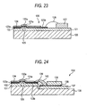
Fig. 23 , thethermal head 120 is affixed to aheat release member 126 for releasing thermal energy generated from theheating area 122a by adhesive in most cases. In addition, asemiconductor chip 127 having a driving circuit for driving theheating resistor 122 is provided on the same surface of theglass layer 121 as the surface where theheating resistor 122, the pair of theelectrodes protection layer 124 are provided, and thesemiconductor chip 127 is electrically connected with theelectrode 123b by awire 128 in most cases. - There is a demand for a miniaturization of a printer using the
thermal head 120, particularly in the case of a household printer. In order to reduce the size of the printer, miniaturization of thethermal head 120 is necessary. - However, since the
semiconductor chip 127 is disposed on the same surface of theglass layer 121 as the surface where theheating resistor 122 and other components are located in thethermal head 120, the size of theglass layer 121 is inevitably large. Therefore, miniaturization of thethermal head 120 and thus size reduction of the printer are difficult. Additionally, the cost increases since the large-sized glass layer 121 is used in thethermal head 120. - As illustrated in
Fig. 23 , thethermal head 120 is affixed to theheat release member 126 for releasing thermal energy from theheating area 122a by adhesive, and thesemiconductor chip 127 having the driving circuit for driving theheating area 122a is provided on the same surface of theglass layer 121 as the surface where theheating resistor 122, the pair of theelectrodes protection layer 124. Thesemiconductor chip 127 is electrically connected with theelectrode 123b facing to thesemiconductor chip 127 by thewire 128. Thesemiconductor chip 127 is higher than a portion where theheating area 122a is provided in thethermal head 120. Thus, in the printer using thethermal head 120, it is necessary to dispose the positions of moving paths of an ink ribbon and a printing medium away from thethermal head 120 so that the ink ribbon and the printing medium do not contact thesemiconductor chip 127. This requirement imposes limitation on the locations of the moving paths of the ink ribbon and the printing medium. - There is a demand for miniaturization of a printer using the
thermal head 120, particularly in the case of a household printer. In order to miniaturize the printer, size reduction of thethermal head 120 is necessary. - In the case of the
thermal head 120, the ink ribbon and the printing medium moving between thethermal head 120 and the platen are positioned substantially perpendicular to thethermal head 120 so that color material can be appropriately transferred onto the printing medium by heat during movement of the ink ribbon and the printing medium between thethermal head 120 and the platen. When the movement of the ink ribbon and the printing medium is substantially perpendicular to thethermal head 120 in the printer, there is a possibility of contact between thesemiconductor chip 127 and the ink ribbon and the printing medium since thesemiconductor chip 127 is higher than the portion having theheating area 122a. In the structure of thethermal head 120, therefore, it is necessary to dispose thesemiconductor chip 127 away from the portion of theheating area 122a so that the contact between thesemiconductor chip 127 and the ink ribbon and the printing medium can be avoided. This requirement increases the size of theglass layer 121 of thethermal head 120, and therefore the cost rises and miniaturization becomes difficult. - In order to overcome these drawbacks, the present inventors further developed a
thermal head 130 shown inFig. 24 . Thethermal head 130 is now discussed as further art related to the invention. Similarly to thethermal head 120 described above, thethermal head 130 includes aglass layer 131 having a substantially circular-arc-shaped projectingportion 131a, and aheating resistor 132, a pair ofelectrodes protection layer 134 are formed on theglass layer 131 in this order. The projectingportion 131a is formed such that aheating area 132a of theheating resistor 132 exposed between the pair of theelectrodes groove 135 filled with air is formed inside theglass layer 131. Thethermal head 130 is affixed to aheat release member 136 by adhesive. According to thethermal head 130, asemiconductor chip 136 is not provided on theglass layer 131 but on another component as arigid substrate 137. In thethermal head 130, theelectrode 133b facing to thesemiconductor chip 136 is electrically connected with aconnection terminal 138 of thesemiconductor chip 136 provided on therigid substrate 137 by awire 139, and the wire bonding portion is sealed byresin 140. According to thethermal head 130, the size of theglass layer 131 is reduced compared with the case of thethermal head 120, and therefore the cost is lowered. - According to the structure of the
thermal head 130, the height of thesemiconductor chip 136 is smaller than the height of the portion having theheating area 132a. However, there is a possibility that the wire bonding portion between theelectrode 133b on theglass layer 131 and theconnection terminal 138 on therigid substrate 137 is positioned higher than the portion of theheating area 132a. Thus, even in thethermal head 130, the positions of the moving paths of the ink ribbon and the printing medium are limited with a necessity for disposing the wire bonding portion away from the portion of theheating area 132a. This requirement makes miniaturization difficult. Accordingly, even in the case of the printer using thethermal head 130, the positions of the moving paths of the ink ribbon and the printing medium moving in the vicinity of thethermal head 130 are limited. -
JP-A-8-216443 -
EP 1403075 A1 describes a thermal head capable of printing two lines at the same time using two lines of heating elements, and to a thermal head capable of performing preheating using one of two lines of heating elements while performing printing using the other one of two lines of heating elements thereby achieving a highspeed printing operation. The thermal head comprises a stainless steel substrate having a substrate projection and a radiating fin for radiating heat generated by heating elements. The substrate projection is formed integrally with the stainless steel substrate so that heat is transferred from a glaze glass layer formed directly on the stainless steel substrate and the substrate projection to the radiating fin. The glaze glass is an insulating element serving to absorb heat remaining in the heating elements and transfer the absorbed heat to the stainless steel substrate. The heating element consists of a pair of heater segments. An intermediate electrode is connected to the heater segments. A common electrode is connected to a conductor pattern of the heating element and also to a power source. A conductor pattern is connected to the heater segment of the heating element and also to a bonding wire. Reference numeral Another conductor pattern is connected to the heater segment of the heating element and also to the common electrode. A control IC is connected to the conductor pattern via the bonding wire. The control IC is connected to the power supply and serves to control an on-off operation of the heating element in accordance with a printer control signal. - Accordingly, there is a need for a compact thermal head, and a compact printer including the thermal head.
- In addition, there is a need for a compact thermal and a compact printer including the thermal head, in which an ink ribbon and a printing medium move along paths disposed at arbitrary positions.
- The above objects are solved by the claimed matter according to the independent claim.
- According to an embodiment of the invention, there is provided a thermal head which includes a head containing a glass layer. The glass layer has a projecting portion on one surface and a concave groove on the other surface at a position opposed to the projecting portion. The head further contains a heating resistor disposed on the projecting portion, and a pair of electrodes disposed on both sides of the heating resistor. The thermal head further includes a rigid substrate on which a control circuit for the head is provided, and a flexible substrate for electrically connecting the head and the rigid substrate.
- According to another embodiment of the invention, there is provided a printer which includes a thermal head. The thermal head contains a head containing a glass layer. The glass layer has a projecting portion on one surface and a concave groove on the other surface at a position opposed to the projecting portion. The head further contains a heating resistor disposed on the projecting portion, and a pair of electrodes disposed on both sides of the heating resistor. The thermal head further contains a rigid substrate on which a control circuit for the head is provided, and a flexible substrate for electrically connecting the head and the rigid substrate.
- According to the thermal head and the printer in these embodiments of the invention, the head and the rigid substrate on which the control circuit is provided are connected by the flexible substrate. Thus, the position of the rigid substrate can be disposed at an arbitrary position. According to the embodiments of the invention, the rigid substrate is disposed along the side of the heat release member by miniaturizing the head and the heat release member, for example, by bending the flexible substrate, so as to make the entire structure compact.
- According to a further embodiment of the invention, there is provided a thermal head disposed at a position opposed to a platen such that an ink ribbon and a printing medium can move between the platen and the thermal head for thermally transferring color material of the ink ribbon onto the printing medium by applying thermal energy to the ink ribbon. The thermal head includes a head containing a glass layer. The glass layer has a projecting portion on one surface and a concave groove on the other surface at a position opposed to the projecting portion. The head further contains a heating resistor disposed on the projecting portion, and a pair of electrodes disposed on both sides of the heating resistor. The thermal head includes a heat release member on which the head is provided, a rigid substrate on which a control circuit for the head is provided, and a flexible substrate for electrically connecting the head and the rigid substrate. A semiconductor chip having a driving circuit for driving the heating resistor is mounted on one of the surfaces of the flexible substrate. The flexible substrate is bent so that the rigid substrate can be disposed along the side of the heat release member.
- According to a still further embodiment of the invention, there is provided a printer which includes a thermal head disposed at a position opposed to a platen such that an ink ribbon and a printing medium can move between the platen and the thermal head for thermally transferring color material of the ink ribbon onto the printing medium by applying thermal energy to the ink ribbon. The thermal head includes a head containing a glass layer. The glass layer has a projecting portion on one surface and a concave groove on the other surface at a position opposed to the projecting portion. The head further contains a heating resistor disposed on the projecting portion, and a pair of electrodes disposed on both sides of the heating resistor. The thermal head further includes a heat release member on which the head is provided, a rigid substrate on which a control circuit for the head is provided, and a flexible substrate for electrically connecting the head and the rigid substrate. A semiconductor chip having a driving circuit for driving the heating resistor is mounted on one of the surfaces of the flexible substrate. The flexible substrate is bent so that the rigid substrate can be disposed along the side of the heat release member.
- According to the thermal head and the printer in these embodiments of the invention, the head and the rigid substrate on which the control circuit is provided are connected by the flexible substrate. The rigid substrate is disposed along the side of the heat release member by bending the flexible substrate. Accordingly, the structure can be compact, and the ink ribbon and the printing medium can move along paths disposed at arbitrary positions.
-
-
Fig. 1 schematically illustrates a printer including a thermal head according to an embodiment of the invention. -
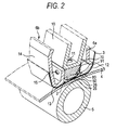
Fig. 2 is a partial perspective view showing the positional relation between the thermal head and ribbon guides. -
Fig. 3 is a perspective view of the thermal head. -
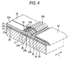
Fig. 4 is a partial perspective view of the thermal head. -
Figs. 5A and 5B are cross-sectional views of a head, whereFig. 5A is a cross-sectional view showing the entire structure of the head, andFig. 5B is an enlarged partial cross-sectional view showing a distal end area of a groove. -
Fig. 6 is a plan view of the head. -
Fig. 7 is a cross-sectional view of a head in another example. -
Figs. 8A and 8B are cross-sectional views of a head in a further example, whereFig. 8A is a cross-sectional view showing the entire structure of the head, andFig. 8B is an enlarged partial cross-sectional view showing a projecting portion. -
Fig. 9 is a cross-sectional view only showing a glass layer of the head shown inFigs. 8A and 8B . -
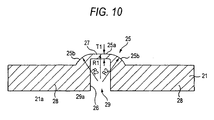
Fig. 10 is a cross-sectional view of the glass layer where a radius of curvature on both sides of the projecting portion is smaller than a radius of curvature at the central area of the projecting portion. -
Fig. 11 is a cross-sectional view of the glass layer having reinforcing portions. -
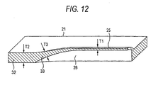
Fig. 12 is a partial cross-sectional view of the glass layer shown inFig. 11 . -
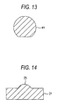
Fig. 13 is a cross-sectional view of glass as a material for the glass layer. -
Fig. 14 is a cross-sectional view of the glass layer. -
Fig. 15 is a cross-sectional view of a condition where a heating resistor and a pair of electrodes are provided on the glass layer by pattern formation. -
Fig. 16 is a cross-sectional view showing a condition where a resistor protecting layer is provided over the heating resistor and the pair of the electrodes. -
Fig. 17 is a partial cross-sectional view of a condition where the groove is formed by a cutter. -
Fig. 18 is a partial perspective view of the thermal head. -
Fig. 19 is a cross-sectional view showing a condition where the glass layer is bonded to a heat release member by an adhesive layer. -
Fig. 20 is a cross-sectional view of a thermal head in related art. -
Fig. 21 is a cross-sectional view of the thermal head shown as an art related to the embodiment of the invention. -
Fig. 22 is a cross-sectional view of the thermal head shown as another art related to the embodiment of the invention. -
Fig. 23 is a cross-sectional view showing a condition where the thermal head shown inFig. 22 is disposed on a heat release member with a semiconductor chip provided on a glass layer. -
Fig. 24 is a cross-sectional view showing a condition where the thermal head shown as the art related to the embodiment of the invention and a semiconductor chip provided on a rigid substrate are electrically connected by wire bonding. - A thermal transfer type printer using a thermal head according to an embodiment of the invention is hereinafter described in detail with reference to the drawings.
- A thermal transfer type printer 1 (hereinafter referred to as printer 1) shown in
Fig. 1 is a sublimation type printer which sublimates color material of an ink ribbon and transfers the sublimated color material onto a printing medium. The printer 1 uses athermal head 2 according to the embodiment of the invention as a recording head. The printer 1 sublimates color material of anink ribbon 3 and thermally transfers the color material onto aprinting medium 4 by applying thermal energy generated from thethermal head 2 to theink ribbon 3, thereby printing color images and characters on theprinting medium 4. The printer 1 is a household printer, and can print on the printing medium such as post cards. - The
ink ribbon 3 used herein is made of long resin film. Theink ribbon 3 before thermal transfer is wound around asupply spool 3a, and theink ribbon 3 after thermal transfer is wound around a windingspool 3b and accommodated in an ink cartridge. Atransfer layer 3c which includes an ink layer having yellow color material, an ink layer having magenta color material, an ink layer having cyan color material, and a laminate layer having a laminate film to be thermally transferred on theprinting medium 4 so as to increase retainability of images and characters printed on theprinting medium 4 is repeatedly formed on one surface of the long resin film of theink ribbon 3. - As illustrated in
Fig. 1 , the printer 1 includes thethermal head 2, aplaten 5 disposed at a position opposed to thethermal head 2, a plurality of ribbon guides 6a and 6b for determining the movement direction of the attachedink ribbon 3, apinch roller 7a and acapstan roller 7b for guiding theprinting medium 4 such that theprinting medium 4 can move between thethermal head 2 and theplaten 5 with theink ribbon 3, adischarge roller 8 for discharging theprinting medium 4 after printing, and aconveyance roller 9 for conveying theprinting medium 4 toward thethermal head 2. As illustrated inFig. 2 , thethermal head 2 is attached to anattachment member 10 provided on a housing of the printer 1 by a fixingmember 11 such as a screw, and in this manner thethermal head 2 is fixed to the printer 1. - The ribbon guides 6a and 6b for guiding the
ink ribbon 3 are disposed before and behind thethermal head 2, i.e., the entrance side and the discharge side of theink ribbon 3 with respect to thethermal head 2. The ribbon guides 6a and 6b positioned before and behind thethermal head 2 guide theink ribbon 3 and theprinting medium 4 into the space between thethermal head 2 and theplaten 5 such that the overlappedink ribbon 3 and theprinting medium 4 can contact thethermal head 2 substantially at right angles. Thus, thermal energy generated from thethermal head 2 can be securely applied to theink ribbon 3. - The
ribbon guide 6a is disposed on the entrance side of theink ribbon 3 with respect to thethermal head 2. Theribbon guide 6a has a curvedlower end surface 12 so that theink ribbon 3 supplied from thesupply spool 3a positioned above thethermal head 2 can enter between thethermal head 2 and theplaten 5. - The
ribbon guide 6b is disposed on the discharge side of theink ribbon 3 with respect to thethermal head 2. Theribbon guide 6b has aflat portion 13 having a flat lower end, and a separatingportion 14 projecting upward substantially in the vertical direction from the end of theflat portion 13 opposite to thethermal head 2 to separate theink ribbon 3 from theprinting medium 4. Theribbon guide 6b cools the heat of theink ribbon 3 after thermal transfer by theflat portion 13. After cooled on theflat portion 13, theink ribbon 3 rises in the direction substantially perpendicular to theprinting medium 4 along the separatingportion 14 to be separated from theprinting medium 4. Theribbon guide 6b is attached to thethermal head 2 by a fixingmember 15 such as a screw. - According to the printer 1 having this structure, the
ink ribbon 3 moves between thethermal head 2 and theplaten 5 in the winding direction in accordance with rotation of the windingspool 3b in the winding direction with theplaten 5 pressed against thethermal head 2 as illustrated inFig. 1 . Theprinting medium 4 sandwiched between thepinch roller 7a and thecapstan roller 7b moves in the discharge direction (direction indicated by arrow A inFig. 1 ) in accordance with the rotation of thecapstan roller 7b and thedischarge roller 8 in the discharge direction. In printing, thermal energy is initially applied from thethermal head 2 to the yellow ink layer of theink ribbon 3 to thermally transfer the yellow color material onto theprinting medium 4 overlapping with theink ribbon 3 during movement. After thermal transfer of the yellow color material, theconveyance roller 9 is rotated toward the thermal head 2 (direction indicated by arrow B inFig. 1 ) so that the magenta color material can be thermally transferred to the image forming area for forming images and characters to which area the yellow color material has been thermally transferred. As a result, theprinting medium 4 moves in the reverse direction toward thethermal head 2 to reach a position where the starting end of the image forming area comes opposed to thethermal head 2, thereby the magenta ink layer of theink ribbon 3 comes opposed to thethermal head 2. Then, thermal energy is applied to the magenta ink layer in the same manner as in the thermal transfer of the yellow ink layer so that the magenta color material can be thermally transferred to the image forming area of theprinting medium 4. The cyan color material and the laminate film are thermally transferred in the similar manner to the method of the thermal transfer of the magenta color material. After sequential thermal transfer of the cyan color material and the laminate film onto theprinting medium 4, printing of color images and characters is completed. - The
thermal head 2 used in the printer 1 can print images having edges as margins at both ends in the direction perpendicular to the moving direction of theprinting medium 4, that is, in the width direction of theprinting medium 4. In addition, the printer 1 can print images having no edge as margin. Thethermal head 2 has a width larger than the width of theprinting medium 4 in a direction indicated by an arrow L inFig. 3 so that color material can be thermally transferred onto theprinting medium 4 including both ends of the medium 4 in the width direction. - According to the structure of the
thermal head 2, ahead 20 for carrying out thermal transfer of the color material of theink ribbon 3 to theprinting medium 4 is attached to aheat release member 50 as illustrated inFig. 3 . As can be seen fromFigs. 4 and5A , thehead 20 has aglass layer 21, and aheating resistor 22, a pair ofelectrodes heating resistor 22, and aresistor protecting layer 24 provided on and around theheating resistor 22 are formed on theglass layer 21. Thethermal head 2 hasheating areas 22a as portions of theheating resistor 22 exposed between the pair of theelectrodes electrode 23a, theheating resistor 22, and theresistor protecting layer 24 are formed on the upper surface of theglass layer 21 as a base layer of thehead 20. - As illustrated in
Figs. 4 and5A , theglass layer 21 has a substantially circular-arc-shaped projectingportion 25 on the outer surface facing theink ribbon 3, and agroove 26 on the inner surface. Theglass layer 21 is substantially rectangular and made of glass having a softening point of about 500 degrees Celsius, for example. The projectingportion 25 is positioned substantially at the center of theglass layer 21 in the width direction, and is substantially semi-cylindrical in the length direction (L direction inFig. 4 ). Since the substantially circular-arc-shaped projectingportion 25 is provided on the surface of theglass layer 21 opposed to theink ribbon 3, theheating areas 22a disposed on the projectingportion 25 can smoothly contact theink ribbon 3. Thus, the thermal energy generated from theheating areas 22a of theheating resistor 22 can be appropriately applied to theink ribbon 3. - A
central area 25a of the projectingportion 25 may be substantially flat. Theglass layer 21 may be made of any material as long as it has predetermined surface properties and thermal characteristics, for which material glass is typically used. Examples of glass herein include synthetic jewelry and artificial stone such as artificial crystal, artificial ruby, and artificial sapphire, high-density ceramic, and others. - As illustrated in
Figs. 4 and5A , thegroove 26 formed on the inner surface of theglass layer 21 is opposed to arow 22b of theheating areas 22a formed substantially in a linear direction along the length of the thermal head 2 (L direction inFig. 4 ) on the projectingportion 25, and concaved toward theheating areas 22a. In theglass layer 21, a space between the projectingportion 25 and thegroove 26 is aheat accumulating portion 27 for accumulating thermal energy generated from theheating areas 22a. - Since the
glass layer 21 has thegroove 26, the thermal energy does not conduct throughout the layer because of the characteristic of the air that the air has lower thermal conductivity than that of glass. Thus, thermal energy is easily accumulated on theheat accumulating portion 27 formed between theheating areas 22a and thegroove 26. Since thermal energy is not released throughout the layer by the presence of thegroove 26 in the structure of theglass layer 21, heat release of thermal energy generated from theheating areas 22a can be reduced and therefore the quantity of heat supplied to theink ribbon 3 can be increased. As a result, thermal efficiency of thethermal head 2 can be improved by the adoption of theglass layer 21. Moreover, at the time of thermal transfer of the color material onto theprinting medium 4, the temperature of the color material can be immediately increased to the sublimation temperature with reduced power by utilizing the thermal energy accumulated on theheat accumulating portion 27 according to the structure of theglass layer 21. Thus, thermal efficiency of thethermal head 2 can be enhanced. Furthermore, according to theglass layer 21 having thegrove 26, the thickness of theheat accumulating portion 27 is reduced and therefore the quantity of accumulated heat is decreased. As a result, heat can be released in a short time, and the temperature of thethermal head 2 can be immediately lowered when theheating areas 22a do not generate heat. According to theglass layer 21 having thegroove 26, therefore, thermal efficiency and responsiveness of thethermal head 2 can be improved. Thus, thethermal head 2 having excellent responsiveness can print high-quality images and characters at high speed with reduced power without causing problems such as blur of images and characters. - As illustrated in
Fig. 5A , theheating resistor 22 for generating thermal energy is formed on the surface of theglass layer 21 on which the projectingportion 25 is provided. Theheating resistor 22 is made of material which is highly resistant and has thermal resistance such as Ta-N and Ta-SiO2. Theheating areas 22a of theheating resistor 22, which are exposed between the pair of theelectrodes portion 25 substantially in a linear direction. Each of theheating areas 22a is slightly larger than the dot size of thermal transfer so that thermal energy can be dispersed, and has a substantially rectangular or square shape. Theheating resistor 22 is provided on theglass layer 21 by pattern formation using photolithography technology. - The pair of the
electrodes heating resistor 22 supplies current from a power source not shown in detail to theheating areas 22a such that theheating areas 22a can generate heat. The pair of theelectrodes Figs. 4 and6 , the pair of theelectrodes common electrode 23a electrically connected with all theheating areas 22a anddiscrete electrodes 23b each of which is electrically and individually connected with the correspondingheating area 22a, respectively. Thecommon electrode 23a and thediscrete electrodes 23b are separated from each other with theheating areas 22a interposed therebetween. - The
common electrode 23a is disposed on theglass layer 21 on the side opposite to the side to which a power supplyflexible substrate 80 to be described later is affixed with the projectingportion 25 of theglass layer 21 interposed between thecommon electrode 23a and the power supplyflexible substrate 80. Thecommon electrode 23a is electrically connected with all theheating areas 22a. Both ends of thecommon electrode 23a are expanded toward the side to which the power supplyflexible substrate 80 is affixed along the shorter side of theglass layer 21 to be electrically connected with the power supplyflexible substrate 80. Thecommon electrode 23a is electrically connected via the power supplyflexible substrate 80 with arigid substrate 70 which is electrically connected with a not-shown power source such that the power source and therespective heating areas 22a can be electrically connected. - The
discrete electrodes 23b are disposed on theglass layer 21 on the side to which signalflexible substrates 90 to be described later are affixed with the projectingportion 25 of theglass layer 21 interposed between thediscrete electrodes 23b and the signalflexible substrates 90. Each of thediscrete electrodes 23b is provided for thecorresponding heating area 22a with one-to-one correspondence. Thediscrete electrodes 23b are electrically connected with the signalflexible substrates 90 connected with a control circuit for controlling the operation of theheating areas 22a on therigid substrate 70. - The
common electrode 23a and thediscrete electrodes 23b supply current to theheating areas 22a selected by the circuit for controlling the operation of theheating areas 22a for a predetermined period of time to cause theheating areas 22a to generate heat until the temperature of the color material rises to the sublimation temperature sufficient for thermal transfer. - According to the structure of the
head 20, it is not necessary to provide theheating resistor 22 on the entire surface of theglass layer 21. It is possible to provide theheating resistor 22 on a part of the projectingportion 25 and dispose the ends of thecommon electrode 23a and thediscrete electrodes 23b on theheating resistor 22. - As illustrated in
Fig. 4 , theresistor protecting layer 24 disposed at the outermost position of thehead 20 covers the entire surfaces of theheating resistor 22 and thecommon electrode 23a and the ends of thediscrete electrodes 23b on theheating area 22a side to protect theheating areas 22a and the pair of theelectrodes heating areas 22a from friction caused by the contact between thethermal head 2 and theink ribbon 3 or others. Theresistor protecting layer 24 is made of inorganic material including metal which has excellent mechanical properties such as high strength and abrasion resistance and excellent thermal properties such as heat resistance, thermal shock resistance and thermal conductivity under a high-temperature environment. An example of the material for theresistor protecting layer 24 is SIALON (product name) containing silicon (Si), aluminum (Al), oxygen (O), and nitrogen (N). - According to the
head 20 having the above structure, thegroove 26 is formed such that a width W1 of thegroove 26 formed at the position opposed to therow 22b of theheating areas 22a provided on the inner surface of theglass layer 21 substantially in a linear direction along the length of the head 20 (L direction inFig. 4 ), that is, a width between the cross points of extension lines of wall surfaces 30 of thegroove 26 and an extension line of aceiling surface 31a of thegroove 26, becomes equivalent to or larger than a length. L1 of theheating areas 22a as illustrated inFigs. 4 ,5A and 5B . By setting the width W1 of thegroove 26 of theglass layer 21 to a length equivalent to or larger than the length L1 of theheating areas 22a, thermal efficiency of thethermal head 2 can be further improved. - More specifically, when the width W1 of the
groove 26 of theglass layer 21 is established as a length equivalent to or larger than the length L1 of theheating areas 22a, the thickness at both ends of theheat accumulating portion 27 becomes smaller than that in the case where the width W1 of thegroove 26 is smaller than the length L1 of theheating areas 22a. Thus, thermal energy accumulated on theheat accumulating portion 27 is not easily released from both ends of theheat accumulating portion 27 toward an area therearound, that is, a surroundingarea 28 around thegroove 26. Heat release is reduced particularly when the width W1 of thegroove 26 of theglass layer 21 is larger than the length of theheating areas 22a compared with the case where the width W1 is equal to the length of theheating areas 22a since the thickness at both ends of theheat accumulating portion 27 in the former case is smaller than that in the latter case. In the structure of theglass layer 21, therefore, heat release toward the surroundingarea 28 is reduced. As a result, the quantity of heat supplied to theink ribbon 3 is further increased, and thermal efficiency of thethermal head 2 can be further improved. - The length of the
heating areas 22a is 200 µm, for example. The allowable width of thegroove 26 is in the range from 50 µm to 700 µm, and preferably in the range from 200 µm to 400 µm. - As illustrated in
Figs. 5A and10 , a radius of curvature R2 at bothsides 25b of the projectingportion 25 of theglass layer 21 is smaller than a radius of curvature R1 at thecentral area 25a (R1>R2) . For example, the radius of curvature R1 at thecentral area 25a of theglass layer 21 is 2.5 µm, and the radius of curvature R2 at thesides 25b is 1.0 µm. When the projectingportion 25 of theglass layer 21 is formed such that the radius of curvature R2 at thesides 25b is smaller than the radius of curvature R1 at thecentral area 25a, the thickness of theglass layer 21 at the position between thesides 25b and thegroove 26 becomes smaller, that is, the thickness at both ends of theheat accumulating portion 27 becomes smaller, than that in the case where the radius of curvature R2 at thesides 25b is equal to or larger than the radius of curvature R1 at thecentral area 25a (R1≤R2). As a result, the quantity of accumulated heat on theheat accumulating portion 27 is further decreased, and thus the quantity of heat released from both ends to the surroundingarea 28 of thegroove 26 is further reduced. Consequently, thermal efficiency can be further increased. When the radius of curvature R2 at thesides 25b of the projectingportion 25 of theglass layer 21 is smaller than the radius of curvature R1 at thecentral area 25a, the width of the projectingportion 25 of theglass layer 21 is reduced. As a result, the entire layer can be made compact. - As illustrated in
Fig. 5A , the wall surfaces 30 extend upward substantially in the vertical direction from the sides of thegroove 26 opposite to theheating areas 22a, that is, abase end 29 of thegroove 26. According to theglass layer 21 having thegroove 26 thus formed, pressure applied from the projectingportion 25 to bothends 29a at thebase end 29 of thegroove 26 is not concentrated on theends 29a but dispersed toward abottom surface 21a of theglass layer 21 when theplaten 5 presses thethermal head 2. Thus, physical strength against the press by theplaten 5 can be increased. Accordingly, deformation and breakage of theends 29a of theglass layer 21 caused by the press from theplaten 5 can be prevented, and therefore deformation and breakage of theglass layer 21 can be avoided. - As illustrated in
Fig. 7 , the width between the wall surfaces 30 of theglass layer 21 opposed to each other in the length direction of theheating areas 22a may be determined such that the width at thebase end 29 is larger than the width at adistal end 31. In the case of theglass layer 21 having this structure, thegroove 26 can be easily separated from a metal mold when thegroove 26 is formed by heat pressing using the metal mold for the reason that the width between the wall surfaces 30 of theglass layer 21 opposed to each other in the length direction of theheating areas 22a at thebase end 29 is larger than the width at thedistal end 31. Thus, theglass layer 21 can be easily formed by using a metal mold, and the production efficiency can be increased. - As illustrated in
Figs. 5A and 5B , bothcorners 31b of theceiling surface 31a at thedistal end 31 of thegroove 26 of theglass layer 21 are substantially circular-arc-shaped, and theceiling surface 31a between thecorners 31b is substantially flat. Since thecorners 31b at thedistal end 31 of thegroove 26 are substantially circular-arc-shaped, pressure applied from the projectingportion 25 to thecorners 31b when theplaten 5 presses thethermal head 2 is dispersed and the physical strength against the press by theplaten 5 is increased. Thus, deformation and breakage of thecorners 31b at thedistal end 31 of thegroove 26 of theglass layer 21 caused by the press from theplaten 5 can be prevented. - As illustrated in
Figs. 8A, 8B and9 , theceiling surface 31a of thegroove 26 may be substantially circular-arc-shaped similarly to the surface of thecentral area 25a of the projectingportion 25 such that the thickness of theglass layer 21 of thehead 20 shown inFigs. 5A and 5B in the area between theceiling surface 31a at thedistal end 31 of thegroove 26 and the surface of thecentral area 25a of the projectingportion 25, that is, a thickness T1 of the projectingportion 25 becomes substantially constant, or substantially uniform. When theceiling surface 31a of thegroove 26 of theglass layer 21 is concentric with thecentral area 25a of the projectingportion 25 as illustrated inFig. 9 , the thickness T1 of the projectingportion 25 becomes substantially uniform. The thickness T1 of the projectingportion 25 is in the range from 10 µm to 100 µm, preferably in the range from 20 µm to 40 µm. For example, the thickness T1 of 27.5 µm is particularly preferable. According to this structure of theglass layer 21 having the thickness T1 of the projectingportion 25 which is substantially uniform with no variation, stress applied by the press from theplaten 5 is not concentrated on theend corners 31b of thegroove 26. Thus, physical strength increases even when the thickness T1 of the projectingportion 25 of theglass layer 21 is extremely small. Moreover, since the thickness T1 of the projectingportion 25 is substantially uniform, the thickness of theheat accumulating portion 27 becomes substantially uniform. As the thickness of theheat accumulating portion 27 is not variable, thermal balance of theheat accumulating portion 27 is improved, and thermal efficiency and responsiveness of thethermal head 2 are enhanced accordingly. - According to the
thermal head 2 having thehead 20 constructed as above, thermal energy generated from theheating areas 22a is not easily released to theglass layer 21 by the presence of thegroove 26 on theglass layer 21. In addition, theheating areas 22a can generate heat with reduced power until the temperature of the color material reaches the sublimation temperature by utilizing the heat accumulated on theheat accumulating portion 27. Thus, thermal efficiency is improved. Moreover, since the thickness of theheat accumulating portion 27 is reduced and the quantity of accumulated heat is decreased by the presence of thegroove 26 on theglass layer 21, heat is easily released and the responsiveness is enhanced. Accordingly, thermal efficiency and responsiveness of thethermal head 2 can be improved by the presence of thegroove 26 on theglass layer 21. - Furthermore, according to the structure of the
thermal head 2, the width W1 of thegroove 26 of theglass layer 21 is equivalent to the width of theheating areas 22a or larger than the length L1 of theheating areas 22a. Thus, the thickness at both ends of theheat accumulating portion 27 is reduced, and heat is not easily released from theheat accumulating portion 27. As a result, release of thermal energy generated from theheating areas 22a is decreased, and thermal efficiency is further improved. - Concerning thermal efficiency, since the radius of curvature R2 at both sides of the projecting
portion 25 of theglass layer 21 in thethermal head 2 is smaller than the radius of curvature R1 at thecentral area 25a of the projectingportion 25, the thickness at both sides of theheat accumulating portion 27 is decreased and heat release from theheat accumulating portion 27 is further reduced. Thus, release of thermal energy generated from theheating areas 22a is further reduced, and thermal efficiency is further increased. - According to the structure of the
thermal head 2, thegroove 26 of theglass layer 21 is so formed as to extend upward substantially in the vertical direction with the circular-arc-shapedend corners 31b formed at thedistal end 31 as illustrated inFigs. 5A and 5B and/or to have the substantially uniform thickness T1 of the projectingportion 25 as illustrated inFigs. 8A and 8B . Thus, physical strength can be increased. Since theglass layer 21 of thethermal head 2 has high physical strength, deformation and breakage of theglass layer 21, particularly deformation and damage of the projectingportion 25 having reduced thickness, caused by the press from theplaten 5 at the time of printing are prevented even when large pressure of about 45 kg per unit area is applied to theglass layer 21. - Accordingly, the
thermal head 2 has excellent thermal efficiency and responsiveness, and theglass layer 21 and the projectingportion 25 are not deformed nor damaged by the press from theplaten 5. Thus, high-quality images and characters can be printed with reduced power at high speed. In addition, according to the structure of thethermal head 2, it is possible that thegroove 26 is so formed that the width between the wall surfaces 30 of thegroove 26 at thebase end 29 is larger than the width at thedistal end 31 as illustrated inFig. 7 . In this case, when thegroove 26 is formed by heat pressing using a metal mold, for example, the mold can be easily separated. Thus, production efficiency increases. - As illustrated in
Figs. 11 and12 , thegroove 26 of theglass layer 21 of thehead 20 is provided at the position opposed to therow 22b of theplural heating areas 22a arranged substantially in a linear direction along the length of the head 20 (L direction inFig. 11 ), and a first reinforcingportion 32 is provided on both sides of thegroove 26 in the linear arrangement direction of theheating areas 22a. The first reinforcingportion 32 is formed by increasing the thickness of theglass layer 21. A thickness T2 of the first reinforcingportion 32 is larger than the thickness T1 of the projecting portion 25 (T2>T1). Since the first reinforcingportion 32 having the thickness T2 larger than the thickness T1 of the projectingportion 25 is provided on both sides of thegroove 26 in the longitudinal direction, the projectingportion 25 of theglass layer 21 is reinforced. Thus, when theplaten 5 presses theglass layer 21, deformation and breakage of the projectingportion 25 of theglass layer 21 caused by the press from theplaten 5 can be prevented. - Additionally, as illustrated in
Figs. 11 and12 , a second reinforcingportion 33 having a thickness T3 which gradually increases from the ends of the projectingportion 25 toward the first reinforcingportion 32 is formed inside the first reinforcingportion 32 in addition to the first reinforcingportion 32. Since the second reinforcingportion 33 as well as the first reinforcingportion 32 is formed on theglass layer 21, the projectingportion 25 can be further reinforced. Thus, physical strength of the projectingportion 25 of theglass layer 21 can be increased, and deformation and breakage of the projectingportion 25 caused by the press from theplaten 5 can be further securely prevented. - According to the structure of the
thermal head 2, the first reinforcingportion 32 and the second reinforcingportion 33 are provided on both sides of theglass layer 21 in the linear arrangement direction of theheating areas 22a. Thus, physical strength of theglass layer 21 can be increased, and deformation and breakage of theglass layer 21, particularly deformation and breakage of the projectingportion 25 having a reduced thickness can be prevented even when large pressure is applied to theglass layer 21. - The
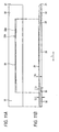
head 20 having theglass layer 21 constructed as above is manufactured by the following method. Initially, as illustrated inFig. 13 ,glass 41 as a material for theglass layer 21 is prepared. Then, as illustrated inFig. 14 , theglass layer 21 having the projectingportion 25 on the upper surface is formed from theglass 41 by heat pressing or other methods. - Subsequently, material which is highly resistant and has heat resistance is formed into a resistor film which will become the
heating resistor 22 and is provided on the surface of theglass layer 21 where the projectingportion 25 is provided by using a thin film formation technology such as sputtering, though the details of this method are not shown in the figure. Material having high electric conductivity such as aluminum is formed into conductive films which will become the pair of theelectrodes - Then, as illustrated in
Fig. 15 , theheating resistor 22 and the pair of theelectrodes heating resistor 22 is exposed between the pair of theelectrodes heating areas 22a. Theglass layer 21 is exposed in the areas where theheating resistor 22 and the pair of theelectrodes - Next, as illustrated in
Fig. 16 , SIALON or other material is formed into theresistor protecting layer 24 having a predetermined thickness and provided on theheating resistor 22 and the pair of theelectrodes - Subsequently, as illustrated in
Fig. 17 , theconcave groove 26 is formed on the surface of theglass layer 21 opposite to the surface where the projectingportion 25 has been formed, that is, the surface which becomes the inner surface of thethermal head 2 at the position opposed to therow 22b of theheating areas 22a by cutting using acutter 42, thereby completing manufacture of thehead 20. By using thecutter 42 for forming thegroove 26, the first reinforcingportion 32 and the second reinforcingportion 33 can be formed on theglass layer 21 by a series of cutting steps as illustrated inFig. 17 . - Hydrofluoric acid treatment may be applied to the inner surface of the
groove 26 after forming thegroove 26 by cutting so as to remove flaws given to the inner surface of thegroove 26. Thegroove 26 may be formed by other methods such as etching or heat pressing other than mechanical processing such as cutting. - In the case of forming the
groove 26 shown inFig. 7 which has the wall surfaces 30 expanding from thedistal end 31 toward thebase end 29, thegroove 26 may be formed by heat pressing using a metal mold since the metal mold can be easily separated. When thegroove 26 is formed by heat pressing, thegroove 26 may be formed simultaneously with the formation of the projectingportion 25 by using the upper mold for the projectingportion 25 and the lower mold for thegroove 26. - Since the entire structure of the
head 20 is formed by theglass layer 21 without using a ceramic substrate, the number of components not including the ceramic substrate is smaller than the number of components of thethermal head 100 which uses theceramic substrate 101 shown inFig. 20 . Thus, the structure of thehead 20 can be simplified. Accordingly, production efficiency of thethermal head 2 can be improved by the reduction of the number of components. - As illustrated in
Figs. 3 and18 , thethermal head 2 having thehead 20 thus constructed is disposed on theheat release member 50 via anadhesive layer 60. Thehead 20 and therigid substrate 70 having the control circuit for thehead 20 and the like are electrically connected by the power supplyflexible substrate 80 and the signalflexible substrates 90. According to the structure of thethermal head 2, therigid substrate 70 is brought to a position facing the side of theheat release member 50 by bending the power supplyflexible substrate 80 and the signalflexible substrates 90 toward theheat release member 50. - The
heat release member 50 efficiently releases thermal energy generated from thehead 20 at the time of thermal transfer of the color material, and is made of material having high heat conductivity such as aluminum. As illustrated inFigs. 3 and18 , anattachment projection 51 to which theheat 20 is attached is formed on the upper surface of theheat release member 50 substantially at the center in the width direction throughout the length of the heat release member 50 (L direction inFig. 18 ). Ataper 52 for bending the power supplyflexible substrate 80 and the signalflexible substrates 90 along the side of theheat release member 50 is provided at the upper end of the side of theheat release member 50 facing to the bent areas of the power supplyflexible substrate 80 and the signalflexible substrates 90. Afirst notch 53 for positioning therigid substrate 70 along the side of theheat release member 50 is formed at the lower end of thetaper 52. Also, asecond notch 54 is formed on theheat release member 50 so that semiconductor chips 91 to be described later formed on the signalflexible substrates 90 can be disposed at positions facing to theheat release member 50. - As illustrated in
Fig. 19 , thehead 20 is attached to theattachment projection 51 of theheat release member 50 via theadhesive layer 60. Theadhesive layer 60 is formed by adhesive having thermal conductivity and elasticity. Since theadhesive layer 60 has thermal conductivity, theadhesive layer 60 can efficiently release heat generated from thehead 20 to theheat release member 50. Since theadhesive layer 60 has elasticity, thehead 20 is not separated from theheat release member 50 by the heat release from thehead 20 even when thehead 20 and theheat release member 50 differently expand or contract due to different coefficients of thermal expansion of theheat release member 50 and thehead 20. The thickness of theadhesive layer 60 is about 50 µm, for example. - As illustrated in
Fig. 19 , theadhesive layer 60 is made of resin having thermal conductivity such as hot setting type and liquid silicone rubber, and containsfillers 61 having high hardness and thermal conductivity. Thefillers 61 contained in theadhesive layer 60 are particulate or linear fillers such as aluminum oxide. Thefillers 61 contained in theadhesive layer 60 function as spacers between thehead 20 and theheat release member 50. Thefillers 61 are not contracted by thehead 20 pressed by theplaten 5, and maintain a constant thickness of theadhesive layer 60 while preventing depression of theends 29a at thebase end 29 of theglass layer 21 toward theheat release member 50. Since theadhesive layer 60 keeps its thickness constant by thefillers 61, pressure applied from the projectingportion 25 to theends 29a at thebase end 29 of thegroove 26 at the time of the press of theplaten 5 against thehead 20 is dispersed to thebottom surface 21a of theglass layer 21 and received by the entirebottom surface 21a of theglass layer 21. Furthermore, in theadhesive layer 60, the pressure applied from theplaten 5 is released in a direction parallel with thebottom surface 21a by the rolling movement of thefillers 61. - Accordingly, depression of the
glass layer 21 of thethermal head 2 toward theheat release member 50 is prevented even when large pressure is applied from theplaten 5 to theglass layer 21, and therefore deformation and breakage of theglass layer 21 is prevented. - The
fillers 61 contained in theadhesive layer 60 may have a diameter equal to or larger than the thickness of theadhesive layer 60. According to theadhesive layer 60 which contains thefillers 61 having the thickness equivalent to or larger than the thickness of theadhesive layer 60, theadhesive layer 60 is not constricted by thehead 20 due to the presence of thefillers 61 at the time of the press of theplaten 5 against thehead 20. Thus, the thickness of theadhesive layer 60 can be more securely maintained, and deformation and breakage of theglass layer 21 can be more securely prevented. - A not-shown power supply line for supplying current from the power source to the
head 20, and a not-shown control circuit for controlling the operation of thehead 20 on which a plurality of electronic components are mounted are provided on therigid substrate 70 disposed facing to the side of theheat release member 50 shown inFig. 3 . As illustrated inFig. 3 ,flexible substrates 71 as power supply lines and signal lines are electrically connected with therigid substrate 70. Therigid substrate 70 is disposed in thefirst notch 53 formed on the side of theheat release member 50. Both ends of therigid substrate 70 are fixed to theheat release member 50 by fixingmembers 72 such as screws. - As illustrated in
Figs. 3 and6 , one end of the power supplyflexible substrate 80 electrically connected with therigid substrate 70 is electrically connected with the not-shown power supply line of therigid substrate 70, and the other end is electrically connected with thecommon electrode 23a of thehead 20 so as to electrically connect thecommon electrode 23a of thehead 20 and the line of therigid substrate 70 and supply current to therespective heating areas 22a. The power supplyflexible substrate 80 may electrically connect with thecommon electrode 23a via a film made of insulating resin material containing conductive particles such as anisotropic conductive film (ACF) interposed between the power supplyflexible substrate 80 and thecommon electrode 23a. Since the power supplyflexible substrate 80 and thecommon electrode 23a are electrically connected via the ACF, release of thermal energy generated from theheating areas 22a toward the power supplyflexible substrate 80 via thecommon electrode 23a is prevented. - As illustrated in
Figs. 3 and6 , one end of each of the signalflexible substrates 90 is electrically connected with the not-shown control circuit on therigid substrate 70, and the other end is electrically connected with the correspondingdiscrete electrodes 23b of thehead 20. The signalflexible substrates 90 are plural and disposed in parallel with one another along the length of the thermal head 2 (L direction inFig 3 ). - As illustrated in
Figs. 6 and18 , thesemiconductor chip 91 having driving circuits for driving the correspondingheating areas 22a of thehead 20 is provided on one surface of each of the signalflexible substrates 90. A connectingterminal 92 for electrically connecting thesemiconductor chip 91 and the correspondingdiscrete electrodes 23b is provided on each connecting side of the same surfaces of the signalflexible substrates 90 connected with thehead 20. - As illustrated in
Fig. 18 , thesemiconductor chip 91 provided on each of the signalflexible substrates 90 is disposed on the inner side of the signalflexible substrate 90. As illustrated inFig. 6 , each of the semiconductor chips 90 has ashift register 93 for converting a serial signal corresponding to printing data given from the control circuit of therigid substrate 70 into a parallel signal, and switchingelements 94 for controlling heat generation from theheating areas 22a. Theshift register 93 converts the serial signal corresponding to the printing data into the parallel signal and latches the converted parallel signal. Each of the switchingelements 94 is provided for the correspondingdiscrete electrode 23b equipped on thecorresponding heating area 22a. The parallel signal latched by theshift register 93 controls on and off of the switchingelements 94 to control heat generation from theheating areas 22a by controlling current supply, supply time and other conditions for therespective heating areas 22a. - As illustrated in
Fig. 6 , each of the connectingterminals 92 is provided for the correspondingdiscrete electrodes 23b which are equipped for theheating areas 22a with one-to-one correspondence to electrically connect thediscrete electrodes 23b and thesemiconductor chip 91. As illustrated inFig. 4 , afilm 95 such as an anisotropic conductive film (ACF) is interposed between theglass layer 21 on thediscrete electrodes 23b side and the signalflexible substrate 90 such that the connectingterminals 92 and thediscrete electrodes 23b are electrically connected via the ACF. According to the structure of thethermal head 2, since thediscrete electrodes 23b of thehead 20 and the signalflexible substrates 90 are connected by the ACF made of insulating resin material, release of thermal energy generated from theheating areas 22a toward the signalflexible substrate 90 via thediscrete electrodes 23b is prevented even when the signalflexible substrates 90 are connected in the vicinity of theheating areas 22a. Thus, thermal efficiency is not decreased. Accordingly, in the structure of thethermal head 2 in which thegroove 26 is formed on theglass layer 21 of thehead 20 and thediscrete electrodes 23b and the signalflexible substrates 90 are connected by the ACF, release of thermal energy generated from theheating areas 22a is further reduced, and thermal efficiency is further increased. Since release of thermal energy from theheating areas 22a toward the signalflexible substrates 90 via thediscrete electrodes 23b is prevented by the ACF connection in thethermal head 2, the semiconductor chips 91 provided on the signalflexible substrates 90 can be protected from heat. - Electrical connection between the connecting
terminals 92 and thediscrete electrodes 23b may be made by material which contains resin and has low thermal conductivity such as conductive paste in lieu of thefilm 95 such as ACF. The semiconductor chips 91 of thethermal head 2 may be disposed outside. - An insulating component may be interposed between the
heat release member 50 and the parts of therigid substrate 70, the power supplyflexible substrate 80, and the signalflexible substrates 90 in thethermal head 2 so as to prevent electrical contact and mechanical contact between theheat release member 50 and the semiconductor chips 91 and between therigid substrate 70 and theheat release member 50. - According to the
thermal head 2 thus constructed, the semiconductor chips 91 having the shift registers 93 for converting the serial signal into parallel signal are provided on the signalflexible substrates 90 which electrically connect thediscrete electrodes 23b of thehead 20 and the control circuit of therigid substrate 70. Thus, serial transmission between therigid substrate 70 and the signalflexible substrates 90 can be achieved, resulting in reduction of the number of electrical connections. - Since the
head 20 and therigid substrate 70 are connected by the power supplyflexible substrate 80 and the signalflexible substrates 90 in thethermal head 2 having the above structure, therigid substrate 70 can be disposed at arbitrary positions around thehead 20. As illustrated inFigs. 3 and18 , the semiconductor chips 91 of thethermal head 2 are opposed to thesecond notch 54 formed on theheat release member 50. The power supplyflexible substrate 80 and the signalflexible substrates 90 are curved along thetaper 52 of theheat release member 50 such that the semiconductor chips 91 are located inside. Therigid substrate 70 is disposed in thefirst notch 53 of theheat release member 50. Since therigid substrate 70 is positioned facing to the side of theheat release member 50, thethermal head 2 is made compact, resulting in reduction of the entire size of the printer 1. Accordingly, the printer 1 including thethermal head 2 can be made compact, which has been demanded especially for household printers. - According to the structure of the
thermal head 2, thehead 20 is equipped on theheat release member 50 via theadhesive layer 60. Thus, the structure is simplified and easily manufactured, resulting in increase of production efficiency. Since the semiconductor chips 91 are disposed on the inner side of thethermal head 2, the semiconductor chips 91 can be protected from static electricity. - In the structure of the
thermal head 2 miniaturized by disposing the semiconductor chips 91 inside and therigid substrate 70 facing to the side of theheat release member 50, theribbon guide 6a on the entrance side of theprinting medium 4 can be positioned close to thethermal head 2 as illustrated inFigs. 1 and2 . In the structure of the printer 1 having thethermal head 2, therefore, theink ribbon 3 and theprinting medium 4 can be guided to a position immediately before entrance into the space between thethermal head 2 and theplaten 5, and thereby theink ribbon 3 and theprinting medium 4 can appropriately enter between thethermal head 2 and theplaten 5. Since theink ribbon 3 and theprinting medium 4 enter between thethermal head 2 and theplaten 5 in a proper manner in the printer 1, theink ribbon 3 and theprinting medium 4 contact thethermal head 2 substantially in the vertical direction, allowing thermal energy from thethermal head 2 to be appropriately applied to theink ribbon 3. In addition, the size reduction of thethermal head 2 increases the degree of freedom in designing the moving paths of theink ribbon 3 and theprinting medium 4 which move near thethermal head 2. - Since the semiconductor chips 91 are equipped on the signal
flexible substrates 90 in thethermal head 2, the necessity for providing the semiconductor chips 91 on theglass layer 21 of thehead 20 is eliminated. Thus, the size of theglass layer 21 is reduced and the cost is lowered. - According to the printer 1 having the
thermal head 2 thus constructed, theink ribbon 3 and theprinting medium 4 move between thethermal head 2 and theplaten 5 while being pressed onto thethermal head 2 by theplaten 5 at the time of printing images and characters as illustrated inFigs. 1 and2 . - During this process, large force of about 45 kg per unit area is applied to the
thermal head 2 by theplaten 5. However, as discussed above, physical strength is increased by forming thegroove 26 extending upward substantially in the vertical direction with the circular-arc-shapedcorners 31b at thedistal end 31 on theglass layer 21 as illustrated inFigs. 5A and 5B , by forming the projectingportion 25 having the substantially uniform thickness T1 as illustrated inFigs. 8A and 8B , by forming the first reinforcingportion 32 and the second reinforcingportion 33 at both ends of thehead 20 in the longitudinal direction as illustrated inFig. 11 , and by inserting fillers into theadhesive layer 60 formed between thehead 20 and theheat release member 50. Thus, deformation and breakage of theglass layer 21 caused by the press from theplaten 5 can be prevented. - Then, the color material of the
ink ribbon 3 is thermally transferred onto theprinting medium 4 moving between thethermal head 2 and theplaten 5. During thermal transfer of the color material, the serial signal corresponding to the printing data given from the control circuit of therigid substrate 70 is converted into the parallel signal by the shift registers 93 of the semiconductor chips 91 provided on the signalflexible substrates 90. The converted parallel signal is latched, and on and off time of the switchingelement 94 provided for each of thediscrete electrodes 23b is controlled based on the latched signal. According to thethermal head 2, when the switchingelement 94 is turned on, current flows in theheating area 22a connected with thisswitch element 94 for a predetermined period of time. As a result, theheating area 22a generates heat and applies generated thermal energy to theink ribbon 3, thereby sublimating the color material and thermally transferring the color material on theprinting medium 4. When the switchingelement 94 is turned off, current does not flow in theheating area 22a connecting with this switchingelement 94 and no heat is generated from theheating area 22a. Since thermal energy is not applied to theink ribbon 3, the color material is not transferred to theprinting medium 4. According to the printer 1, serial signals per line of printing data are transmitted from the control circuit of thethermal head 2 to the semiconductor chips 91 of the signalflexible substrate 90, and the above operations are repeated to thermally transfer yellow on the image forming area. After thermal transfer of yellow, magenta, cyan, and the laminate film are sequentially transferred by heat so that an image corresponding one sheet can be printed. - Since the
groove 26 having the width W1 equivalent to or larger than the length L1 of theheating areas 22a is formed on theglass layer 21 of thehead 20 in thethermal head 2, thermal energy generated from theheat areas 22a is not easily released toward theglass layer 21 during thermal transfer of the color material on theink ribbon 3. Thus, thermal energy accumulated on theheat accumulating portion 27 of theglass layer 21 is not easily released to the surroundingarea 28 of thegroove 26, resulting in increase of the quantity of heat supplied to theink ribbon 3. Since the radius of curvature R2 at thesides 25b of the projectingportion 25 of theglass layer 21 is smaller than the radius of curvature R1 at thecentral area 25a of the projectingportion 25 in thethermal head 2, release of thermal energy accumulated on theheat accumulating portion 27 to the surroundingarea 28 is further reduced. Thus, the temperature of theheating portions 22a can be easily increased by utilizing the thermal energy accumulated on theheat accumulating portion 27 of theglass layer 21 in thethermal head 2. Accordingly, thermal efficiency of thethermal head 2 can be improved. Moreover, since thegroove 26 is formed on theglass layer 21 in thethermal head 2, the quantity of accumulated heat on theglass layer 21 is decreased. Thus, the temperature promptly drops when theheating areas 22a do not generate heat, which enhances responsiveness. Accordingly, the printer 1 having improved thermal efficiency and responsiveness can print high-quality images and characters with reduced power at high speed. - As obvious from above, according to the
thermal head 2 which is made compact, deformation and breakage of theglass layer 21 caused by the press from theplaten 5 is prevented, and thermal efficiency and responsiveness are improved. Thus, the printer 1 used as a household device can print high-quality images and characters with reduced power at high speed. - In this embodiment, the
thermal head 2 is included in the household printer 1 used for printing post cards. However, thethermal head 2 can be employed for printers for business use as well as the household printer 1. The size of the printing medium is not limited to that of post cards, but may be L-size photo sheets, ordinary sheets or the like. In the case of these printing media, the printer including thethermal head 2 can similarly print at high speed. - It should be understood by those skilled in the art that various modifications, combinations, sub-combinations and alterations may occur depending on design requirements and other factors insofar as they are within the scope of the appended claims.
Claims (7)
- A thermal head (2), comprising:a head (20) which includesa glass layer (21) containing a projecting portion (25) on one surface and a concave groove (26) on the other surface at a position opposed to the projecting portion (25),a heating resistor (22) disposed on the projecting portion, anda pair of electrodes (23a, 23b) disposed on both sides of the heating resistor (22);a rigid substrate (70) on which a control circuit for the head is provided; anda heat release member (50) on which the head (2) is disposed; characterized bya flexible substrate (80, 90) for electrically connecting the head (20) and the rigid substrate (70); whereinthe rigid substrate (70) is facing the side of the heat release member (50); andthe flexible substrate (80, 90) is bent toward the heat release member (50) so that the rigid substrate (70) can be disposed along the side of the heat release member (50).
- The thermal head (2) according to claim 1, wherein the electrodes of the head (20) and connection terminals of the flexible substrate (80, 90) are electrically connected by resin containing conductive particles.
- A printer (1) comprising:the thermal head (2) according to claim 1 or 2.
- A thermal head (2) according to claim 1 disposed at a position opposed to a platen (5) such that an ink ribbon (3) and a printing medium (4) can move between the platen (5) and the thermal head (2) for thermally transferring color material of the ink ribbon (3) onto the printing medium (4) by applying thermal energy to the ink ribbon (3), comprising:a semiconductor chip (91) having a circuit for driving the heating resistor (22) mounted on one of the surfaces of the flexible substrate (90).
- The thermal head (2) according to claim 4, wherein the semiconductor chip (91) is disposed on the inner surfaces of the bent flexible substrate (90).
- The thermal head (2) according to claim 4, wherein:the semiconductor chip (91) has a shift register (93) for converting a serial signal given from the control circuit on the rigid substrate (70) into a parallel signal; anda corresponding number of the flexible substrate (90) to the number of electrodes (23b) which are provided for the heating resistor (22) with one-to-one correspondence are disposed on the connecting side of the head (20) and have connection terminals for outputting the parallel signal.
- A printer (1) comprising:the thermal head (2) according to claim 4.
Applications Claiming Priority (2)
| Application Number | Priority Date | Filing Date | Title |
|---|---|---|---|
| JP2006075636A JP4506696B2 (en) | 2006-03-17 | 2006-03-17 | Thermal head and printer device |
| JP2006075628A JP4458054B2 (en) | 2006-03-17 | 2006-03-17 | Thermal head and printer device |
Publications (3)
| Publication Number | Publication Date |
|---|---|
| EP1834792A2 EP1834792A2 (en) | 2007-09-19 |
| EP1834792A3 EP1834792A3 (en) | 2010-03-17 |
| EP1834792B1 true EP1834792B1 (en) | 2012-05-23 |
Family
ID=38169291
Family Applications (1)
| Application Number | Title | Priority Date | Filing Date |
|---|---|---|---|
| EP07005298A Expired - Fee Related EP1834792B1 (en) | 2006-03-17 | 2007-03-14 | Thermal head and printer |
Country Status (3)
| Country | Link |
|---|---|
| US (1) | US7843476B2 (en) |
| EP (1) | EP1834792B1 (en) |
| KR (1) | KR20070094525A (en) |
Families Citing this family (9)
| Publication number | Priority date | Publication date | Assignee | Title |
|---|---|---|---|---|
| JP5200255B2 (en) * | 2007-10-23 | 2013-06-05 | セイコーインスツル株式会社 | Heating resistance element and manufacturing method thereof, thermal head and printer |
| US8154575B2 (en) | 2007-10-23 | 2012-04-10 | Seiko Instruments Inc. | Heating resistor element, manufacturing method for the same, thermal head, and printer |
| JP2009184272A (en) * | 2008-02-07 | 2009-08-20 | Sony Corp | Thermal head, thermal printer, and thermal head manufacturing method |
| JP5408695B2 (en) * | 2008-10-27 | 2014-02-05 | セイコーインスツル株式会社 | Manufacturing method of thermal head |
| JP2010100022A (en) | 2008-10-27 | 2010-05-06 | Seiko Instruments Inc | Heating resistance element part |
| US8111273B2 (en) * | 2009-09-30 | 2012-02-07 | Seiko Instruments Inc. | Thermal head, printer, and manufacturing method for thermal head |
| JP2013043335A (en) * | 2011-08-23 | 2013-03-04 | Seiko Instruments Inc | Thermal head, method of producing the same, and thermal printer |
| JP6676369B2 (en) * | 2015-12-25 | 2020-04-08 | ローム株式会社 | Thermal printhead and thermal printer |
| JP7147412B2 (en) | 2018-09-25 | 2022-10-05 | ブラザー工業株式会社 | Liquid ejection device and wiring member |
Family Cites Families (19)
| Publication number | Priority date | Publication date | Assignee | Title |
|---|---|---|---|---|
| DE3435407A1 (en) | 1984-09-27 | 1986-04-03 | Standard Elektrik Lorenz Ag, 7000 Stuttgart | Thermal print head |
| JPS6480433A (en) | 1987-09-22 | 1989-03-27 | Nippon Paint Co Ltd | Surface active agent having optical function and production thereof |
| JPH0242516A (en) * | 1988-08-03 | 1990-02-13 | Nec Corp | Wrong clock detecting system |
| JPH04152642A (en) | 1990-10-17 | 1992-05-26 | Fujitsu Ltd | Paste for adhesion use |
| JPH0516408A (en) | 1991-07-10 | 1993-01-26 | Tokyo Electric Co Ltd | Thermal head |
| JPH05270030A (en) | 1992-03-26 | 1993-10-19 | Tokyo Electric Co Ltd | Thermal head |
| JP2605970B2 (en) | 1993-06-21 | 1997-04-30 | 日本電気株式会社 | Die bonding resin for semiconductor chip and semiconductor device using the same. |
| JPH0890915A (en) | 1994-09-27 | 1996-04-09 | Toppan Printing Co Ltd | Thermal recording medium |
| JPH0890815A (en) | 1994-09-28 | 1996-04-09 | Kyocera Corp | Thermal head |
| JPH08216443A (en) | 1995-02-14 | 1996-08-27 | Ricoh Co Ltd | Thermal head |
| JP3757499B2 (en) | 1996-11-12 | 2006-03-22 | 神鋼電機株式会社 | Thermal head |
| DE69825324T2 (en) | 1998-05-08 | 2005-01-13 | Shinko Electric Co., Ltd. | THERMO HEAD AND THERMAL PRINTER |
| US6335750B2 (en) * | 1999-02-12 | 2002-01-01 | Kabushiki Kaisha Toshiba | Thermal print head |
| JP2001113738A (en) * | 1999-08-11 | 2001-04-24 | Riso Kagaku Corp | Thick film thermal head |
| JP2001253104A (en) | 2000-03-09 | 2001-09-18 | Shinko Electric Co Ltd | Thermal head |
| JP2002307732A (en) | 2001-04-16 | 2002-10-23 | Alps Electric Co Ltd | Thermal head |
| JP2004175085A (en) | 2002-11-24 | 2004-06-24 | Thermal Printer Institute Inc | High density circuit board and method of manufacturing the same |
| JP4398766B2 (en) | 2004-03-30 | 2010-01-13 | アルプス電気株式会社 | Thermal head and manufacturing method thereof |
| JP2006035836A (en) | 2004-07-26 | 2006-02-09 | Thermal Printer Institute Inc | Thermal print head and manufacturing method thereof |
-
2007
- 2007-03-06 US US11/682,606 patent/US7843476B2/en not_active Expired - Fee Related
- 2007-03-14 EP EP07005298A patent/EP1834792B1/en not_active Expired - Fee Related
- 2007-03-16 KR KR1020070025789A patent/KR20070094525A/en not_active Ceased
Also Published As
| Publication number | Publication date |
|---|---|
| US7843476B2 (en) | 2010-11-30 |
| US20080143810A1 (en) | 2008-06-19 |
| EP1834792A3 (en) | 2010-03-17 |
| KR20070094525A (en) | 2007-09-20 |
| EP1834792A2 (en) | 2007-09-19 |
Similar Documents
| Publication | Publication Date | Title |
|---|---|---|
| US7843476B2 (en) | Thermal head and printer | |
| EP1834791B1 (en) | Thermal head and printing device | |
| JP5815836B2 (en) | Thermal head and thermal printer equipped with the same | |
| US8098268B2 (en) | Thermal head and printing device | |
| EP1834794A2 (en) | Thermal head and printing device equipped with the same | |
| EP1834793A2 (en) | Thermal head and printing device | |
| CN101096148B (en) | Thermal head and printer | |
| JP2009184272A (en) | Thermal head, thermal printer, and thermal head manufacturing method | |
| JP2007245671A (en) | Thermal head and printer device | |
| JP4506696B2 (en) | Thermal head and printer device | |
| JP7857321B2 (en) | Thermal heads and thermal printers | |
| CN221067546U (en) | Spliced thermal print head | |
| JPS60242073A (en) | Vertical thermal head | |
| EP3842243B9 (en) | Thermal head and thermal printer | |
| JP6290632B2 (en) | Thermal head and thermal printer equipped with the same | |
| EP3842242B1 (en) | Thermal head and thermal printer | |
| CN108025558A (en) | Thermal head and thermal printer | |
| JP2019064128A (en) | Thermal head and thermal printer | |
| JP2011025629A (en) | Recording head and recorder |
Legal Events
| Date | Code | Title | Description |
|---|---|---|---|
| PUAI | Public reference made under article 153(3) epc to a published international application that has entered the european phase |
Free format text: ORIGINAL CODE: 0009012 |
|
| AK | Designated contracting states |
Kind code of ref document: A2 Designated state(s): AT BE BG CH CY CZ DE DK EE ES FI FR GB GR HU IE IS IT LI LT LU LV MC MT NL PL PT RO SE SI SK TR |
|
| AX | Request for extension of the european patent |
Extension state: AL BA HR MK YU |
|
| PUAL | Search report despatched |
Free format text: ORIGINAL CODE: 0009013 |
|
| AK | Designated contracting states |
Kind code of ref document: A3 Designated state(s): AT BE BG CH CY CZ DE DK EE ES FI FR GB GR HU IE IS IT LI LT LU LV MC MT NL PL PT RO SE SI SK TR |
|
| AX | Request for extension of the european patent |
Extension state: AL BA HR MK RS |
|
| 17P | Request for examination filed |
Effective date: 20100915 |
|
| 17Q | First examination report despatched |
Effective date: 20101026 |
|
| AKX | Designation fees paid |
Designated state(s): DE FR GB |
|
| GRAP | Despatch of communication of intention to grant a patent |
Free format text: ORIGINAL CODE: EPIDOSNIGR1 |
|
| GRAS | Grant fee paid |
Free format text: ORIGINAL CODE: EPIDOSNIGR3 |
|
| GRAA | (expected) grant |
Free format text: ORIGINAL CODE: 0009210 |
|
| AK | Designated contracting states |
Kind code of ref document: B1 Designated state(s): DE FR GB |
|
| REG | Reference to a national code |
Ref country code: GB Ref legal event code: FG4D |
|
| REG | Reference to a national code |
Ref country code: DE Ref legal event code: R096 Ref document number: 602007022796 Country of ref document: DE Effective date: 20120726 |
|
| PLBE | No opposition filed within time limit |
Free format text: ORIGINAL CODE: 0009261 |
|
| STAA | Information on the status of an ep patent application or granted ep patent |
Free format text: STATUS: NO OPPOSITION FILED WITHIN TIME LIMIT |
|
| 26N | No opposition filed |
Effective date: 20130226 |
|
| REG | Reference to a national code |
Ref country code: DE Ref legal event code: R097 Ref document number: 602007022796 Country of ref document: DE Effective date: 20130226 |
|
| GBPC | Gb: european patent ceased through non-payment of renewal fee |
Effective date: 20130314 |
|
| REG | Reference to a national code |
Ref country code: FR Ref legal event code: ST Effective date: 20131129 |
|
| REG | Reference to a national code |
Ref country code: DE Ref legal event code: R119 Ref document number: 602007022796 Country of ref document: DE Effective date: 20131001 |
|
| PG25 | Lapsed in a contracting state [announced via postgrant information from national office to epo] |
Ref country code: GB Free format text: LAPSE BECAUSE OF NON-PAYMENT OF DUE FEES Effective date: 20130314 Ref country code: FR Free format text: LAPSE BECAUSE OF NON-PAYMENT OF DUE FEES Effective date: 20130402 Ref country code: DE Free format text: LAPSE BECAUSE OF NON-PAYMENT OF DUE FEES Effective date: 20131001 |