EP1816480A1 - Oszilloskop mit Frequenzversatz im Eingangsbereich - Google Patents
Oszilloskop mit Frequenzversatz im Eingangsbereich Download PDFInfo
- Publication number
- EP1816480A1 EP1816480A1 EP07002350A EP07002350A EP1816480A1 EP 1816480 A1 EP1816480 A1 EP 1816480A1 EP 07002350 A EP07002350 A EP 07002350A EP 07002350 A EP07002350 A EP 07002350A EP 1816480 A1 EP1816480 A1 EP 1816480A1
- Authority
- EP
- European Patent Office
- Prior art keywords
- frequency
- oscilloscope
- signal
- local oscillator
- analog
- Prior art date
- Legal status (The legal status is an assumption and is not a legal conclusion. Google has not performed a legal analysis and makes no representation as to the accuracy of the status listed.)
- Granted
Links
Images

Classifications
-
- G—PHYSICS
- G01—MEASURING; TESTING
- G01R—MEASURING ELECTRIC VARIABLES; MEASURING MAGNETIC VARIABLES
- G01R1/00—Details of instruments or arrangements of the types included in groups G01R5/00 - G01R13/00 and G01R31/00
- G01R1/02—General constructional details
- G01R1/06—Measuring leads; Measuring probes
- G01R1/067—Measuring probes
- G01R1/06772—High frequency probes
Definitions
- the invention relates to a digital oscilloscope.
- Digital oscilloscopes ie oscilloscopes with digital memory
- the highest input frequency of digital oscilloscopes is basically limited by the analog / digital converter.
- the analog-to-digital converter samples the analog input signal at a fixed sampling rate. According to the Nyquist theorem, the sampling rate must be at least twice as high as the highest frequency in the spectrum of the analog signal to be sampled. In general, however, a much higher sampling frequency than the theoretical limit is used.
- the maximum usable sampling rate depends on the technology of the analog-to-digital converter. Even with modern parallel-operated flash converters, the sampling rate is limited to the lower GHz range.
- the invention has for its object to provide an oscilloscope, which also makes it possible to analyze band-limited signals whose center frequency is much higher than the frequency limit of the analog / digital converter.
- a frequency shifter in an input region of the oscilloscope, which shifts the input measurement signal into a lower frequency range, which shifts can still be processed by the analog / digital converter.
- the input area preferably contains a mixer which mixes the input measurement signal with the signal of a local oscillator for the purpose of frequency reduction.
- the frequency of the local oscillator is preferably variable and adaptable to the center frequency of the input measurement signal.
- the input section with the frequency shifter can be arranged in the main device of the oscilloscope.
- the frequency shifter is already arranged in the probe so that the signal offset in the lower frequency range is already transmitted on the connecting cable between the probe and the input socket of the main device.
- the oscilloscope 1 shows a first exemplary embodiment of the oscilloscope 1 according to the invention.
- the oscilloscope 1 according to the invention also has an analog / digital converter 3 to convert the analog signal and store the digital values in a memory 4.
- the analog / digital converter 3 generates one sample each time a sampling clock AT is sampled.
- the sampling clock AT is generated by a clock generator 5 which is in communication with the analog / digital converter 3.
- the digital values stored in the memory 4 can then be displayed in their chronological order on a display 6.
- the frequency of the sampling clock AT must be at least twice as high as the highest frequency in the spectrum of the analog signal.
- higher sampling rates are used to increase signal resolution.
- the sampling rate is 8 GHz and the bandwidth of the analog / digital converter is limited to 2 GHz, that is, in the analog / digital converter 3, an analog signal in the range between 0 and 2 GHz abut.
- the invention sets in and proposes to offset by a suitably designed input area 7, the input measurement signal in its frequency and thus supply the analysis.
- the input measurement signal MS must be band limited accordingly, ie the Bandwidth of the input measurement signal MS must not be greater than the frequency limitation of the analog / digital converter. In the example given above, the bandwidth must not exceed 2 GHz.
- the input region 7 of the oscilloscope 1 has a corresponding frequency conversion device 8, which in the exemplary embodiment consists of a mixer 9 and a local oscillator 10.
- the local oscillator signal generated by the local oscillator 10, which is supplied to the mixer 9, should correspond to the smallest frequency in the spectrum of the measuring signal MS.
- the frequency of the local oscillator 10 should be 50 GHz, for example, so that the spectrum shifted by 50 GHz arises at the output of the mixer 9 0 to 2 GHz and thus can be processed by the analog / digital converter 3.
- the inventive frequency offset 8 at the input of the oscilloscope 1 thus enables the analysis of band-limited measurement signals MS.
- band-limited measurement signals often occur in radio measurement technology, in particular in mobile radio measurement technology, as modulated carrier signals.
- FIG. 2 shows the spectrum of the input measurement signal MS, which has a bandwidth of 2 GHz and extends around the center frequency of 51 GHz.
- Fig. 3 shows the reduced by 50 GHz spectrum, which now extends between 0 and 2 GHz.
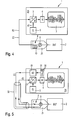
- Fig. 4 shows a first alternative embodiment. Already described elements are provided with matching reference numerals, so that a repetitive description is unnecessary.
- the input region 7 to the frequency converter 8 not within the main unit 20, but within a remote from a probe 21, which is connected via a connecting line 22 to the main unit 20.
- the advantage is that the very high-frequency measurement signal MS does not have to be transmitted directly via the connection line 22. Instead, the frequency-reduced converted analog signal KS is transmitted via the connection line 22.
- both the mixer 9 and the local oscillator 10 are located within the probe 21.
- FIG. 5 shows a third exemplary embodiment of the oscilloscope 1 according to the invention.
- the mixer 9 is arranged within the probe 21.
- the local oscillator 10 can also take a larger spatial design, which is usually required when the local oscillator is constructed as a high-precision synthesizer with multiple PLL stages.
- the mixer 9 can be formed in the simplest case as a diode-ring mixer, which is easily integrated within the probe 21.
- the oscillator signal LS of the local oscillator 10 and the converted analog signal KS generated by the mixer 9 can be guided within a common connection cable 32.
- the frequency converter 8 may also be designed differently and the Frequency conversion can take place over several stages, for example. All features described above or shown in the figures can be combined with each other in the invention as desired.
Landscapes
- Physics & Mathematics (AREA)
- General Physics & Mathematics (AREA)
- Measuring Frequencies, Analyzing Spectra (AREA)
Abstract
Description
- Die Erfindung betrifft ein digitales Oszilloskop.
- Digitale Oszilloskope, d. h. Oszilloskope mit digitalem Speicher, sind aus einer Vielzahl von Druckschriften, beispielsweise aus der
GB 2 399 647 A - In der Praxis besteht aber das Bedürfnis, auch höherfrequente Eingangssignale mit digitalen Oszilloskopen darzustellen. Dies war bisher jedoch nicht möglich.
- Der Erfindung liegt die Aufgabe zugrunde, ein Oszilloskop anzugeben, welches es auch ermöglicht, bandbegrenzte Signale zu analysieren, deren Mittenfrequenz wesentlich höher als die Frequenzbegrenzung des Analog/Digital-Wandlers ist.
- Die Aufgabe wird durch die Merkmale des Anspruchs 1 gelöst. Die Unteransprüche enthalten vorteilhafte Weiterbildungen der Erfindung.
- Erfindungsgemäß wird vorgeschlagen, in einem Eingangsbereich des Oszilloskops einen Frequenz-Shifter vorzusehen, welcher das Eingangs-Messsignal in einen niedrigeren Frequenzbereich versetzt (shiftet), welcher durch den Analog/Digital-Wandler noch verarbeitet werden kann.
- Der Eingangsbereich enthält dazu vorzugsweise einen Mischer, welcher das Eingangs-Messsignal mit dem Signal eines lokalen Oszillators für den Zweck der Frequenzverringerung mischt. Die Frequenz des lokalen Oszillators ist vorzugsweise veränderbar und an die Mittenfrequenz des Eingangs-Messsignals anpassbar.
- Der Eingangsbereich mit dem Frequenz-Shifter kann in dem Hauptgerät des Oszilloskops angeordnet sein. Besonders bevorzugt ist der Frequenz-Shifter aber bereits im Tastkopf angeordnet, so dass auf dem Verbindungskabel zwischen dem Tastkopf und der Eingangsbuchse des Hauptgeräts bereits das in den unteren Frequenzbereich versetzte Signal übertragen wird. Alternativ ist es auch möglich, nur den Mischer in dem Tastkopf anzuordnen und den lokalen Oszillator im Hauptgerät vorzusehen und über das Verbindungskabel das Signal des lokalen Oszillators zu übertragen. Wenn das lokale Oszillatorsignal durch einen Synthesizer erzeugt wird, welcher ein relativ großes Bauvolumen erfordert, kann diese Aufteilung sinnvoll sein. Auch ist es dann einfacher, die Frequenz des lokalen Oszillators entsprechend der Vorgabe durch die Bedienperson einzustellen.
- Ausführungsbeispiele der Erfindung werden nachfolgend unter Bezugnahme auf die Zeichnung näher erläutert. In der Zeichnung zeigen:
- Fig.1
- ein Blockschaltbild eines ersten Ausführungsbeispiels des erfindungsgemäßen Oszilloskops;
- Fig. 2
- das Spektrum des bandbegrenzten Eingangssignals;
- Fig. 3
- das Spektrum des im Eingangsbereich frequenzversetzten Messsignals;
- Fig. 4
- ein Blockschaltbild eines zweiten Ausführungsbeispiels des erfindungsgemäßen Oszilloskops und
- Fig. 5
- ein Blockschaltbild eines dritten Ausführungsbeispiels des erfindungsgemäßen Oszilloskops.
- Fig. 1 zeigt ein erstes Ausführungsbeispiel des erfindungsgemäßen Oszilloskops 1. Das Oszilloskop 1 dient zur Vermessung des Ausgangssignals eines Messobjekts (DUT = Device under Test) 2. Wie bei digitalen Oszilloskopen üblich, weist auch das erfindungsgemäße Oszilloskop 1 einen Analog/Digital-Wandler 3 auf, um das Analog-Signal zu konvertieren und die Digitalwerte in einem Speicher 4 abzulegen. Der Analog/Digital-Wandler 3 erzeugt dabei bei jeder Periode eines Abtasttakts AT jeweils einen Abtastwert. Der Abtasttakt AT wird durch einen Taktgenerator 5 erzeugt, der mit dem Analog/Digital-Wandler 3 in Verbindung steht. Die in dem Speicher 4 abgespeicherten Digitalwerte können dann in ihrer zeitlichen Reihenfolge auf einer Anzeigeeinrichtung (Display) 6 angezeigt werden.
- Entsprechend dem Nyquist-Theorem muss die Frequenz des Abtasttakts AT mindestens doppelt so groß sein wie die höchste Frequenz in dem Spektrum des Analog-Signals. Typischerweise werden aber höhere Abtastraten zur Vergrößerung der Signalauflösung verwendet. Im in Fig. 1 dargestellten Beispiel beträgt die Abtastrate 8 GHz und die Bandbreite des Analog/Digital-Wandlers ist auf 2 GHz begrenzt, das heißt im Analog/Digital-Wandler 3 kann ein Analog-Signal im Bereich zwischen 0 und 2 GHz anliegen.
- In der Praxis besteht aber das Bedürfnis auch höherfrequente Signale zu analysieren. An dieser Stelle setzt die Erfindung ein und schlägt vor, durch einen geeignet ausgestalteten Eingangsbereich 7 das Eingangs-Messsignal in seiner Frequenz zu versetzen und somit der Analyse zuzuführen. Das Eingangs-Messsignal MS muss allerdings entsprechend bandbegrenzt sein, d.h. die Bandbreite des Eingangs-Messsignals MS darf nicht größer sein als die Frequenzbegrenzung des Analog/Digital-Wandlers. Im oben angegebenen Beispiel darf die Bandbreite daher 2 GHz nicht überschreiten.
- Der Eingangsbereich 7 des Oszilloskops 1 weist eine entsprechende Frequenzumsetzeinrichtung 8 auf, die im Ausführungsbeispiel aus einem Mischer 9 und einem lokalen Oszillator 10 besteht. Das von dem lokalen Oszillator 10 erzeugte lokale Oszillatorsignal, welches dem Mischer 9 zugeführt wird, sollte der kleinsten Frequenz im Spektrum des Messsignals MS entsprechen. Wenn das Messsignal MS beispielsweise ein Spektrum hat, welches sich zwischen 50 GHz bis 52 GHz erstreckt, so sollte die Frequenz des lokalen Oszillators 10 beispielsweise 50 GHz betragen, so dass am Ausgang des Mischers 9 das um 50 GHz verschobene Spektrum entsteht, welches sich zwischen 0 bis 2 GHz erstreckt und somit von dem Analog/Digital-Wandler 3 verarbeitet werden kann.
- Durch den erfindungsgemäßen Frequenzversetzer 8 am Eingang des Oszilloskops 1 wird somit die Analyse bandbegrenzter Messsignale MS ermöglicht. Solche bandbegrenzten Messsignale treten in der Funk-Messtechnik, insbesondere der Mobilfunk-Messtechnik, häufig als modulierte Trägersignale auf.
- In Fig. 2 ist das Spektrum des Eingangs-Messsignals MS dargestellt, welches eine Bandbreite von 2 GHz hat und sich um die Mittenfrequenz von 51 GHz erstreckt.
- Fig. 3 zeigt das um 50 GHz herabgesetzte Spektrum, welches sich nun zwischen 0 und 2 GHz erstreckt.
- Fig. 4 zeigt ein erstes alternatives Ausführungsbeispiel. Bereits beschriebene Elemente sind mit übereinstimmenden Bezugszeichen versehen, so dass sich eine wiederholende Beschreibung erübrigt. Im Gegensatz zu dem anhand von Fig. 1 beschriebenen Ausführungsbeispiel befindet sich bei dem in Fig. 4 dargestellten Ausführungsbeispiel der Eingangsbereich 7 mit dem Frequenzkonverter 8 nicht innerhalb des Hauptgeräts 20, sondern innerhalb eines davon abgesetzten Tastkopfs 21, welche über eine Verbindungsleitung 22 mit dem Hauptgerät 20 verbunden ist. Der Vorteil besteht darin, dass das sehr hochfrequente Messsignal MS nicht unmittelbar über die Verbindungsleitung 22 übertragen werden muss. Statt dessen wird das in der Frequenz herabgesetzte konvertierte Analog-Signal KS über die Verbindungsleitung 22 übertragen. Bei dem in Fig. 4 dargestellten Ausführungsbeispiel befinden sich sowohl der Mischer 9 als auch der lokale Oszillator 10 innerhalb des Tastkopfs 21.
- Fig. 5 zeigt ein drittes Ausführungsbeispiels des erfindungsgemäßen Oszilloskops 1. Im Gegensatz zu dem in Fig. 4 erläuterten Ausführungsbeispiel ist bei dem in Fig. 5 gezeigten Ausführungsbeispiel nur der Mischer 9 innerhalb des Tastkopfs 21 angeordnet. Der lokale Oszillator 10 hingegen befindet sich innerhalb des Hauptgeräts 20. Dies hat insoweit Vorteile, als der lokale Oszillator 10 bei dieser Ausgestaltung in einfacher Weise beispielsweise durch innerhalb eines Bedienfelds 31 an der Frontseite des Oszilloskops 1 angeordnete Bedienelemente 30 in seiner Frequenz verändert werden kann. Der lokale Oszillator 10 kann dabei auch eine größere räumliche Bauform einnehmen, was in der Regel erforderlich ist, wenn der lokale Oszillator als hochgenauer Synthesizer mit mehreren PLL-Stufen aufgebaut wird. Der Mischer 9 hingegen kann im einfachsten Fall als Dioden-Ringmischer ausgebildet sein, der problemlos innerhalb des Tastkopfs 21 integrierbar ist. Das Oszillatorsignal LS des lokalen Oszillators 10 und das von dem Mischer 9 erzeugte konvertierte Analogsignal KS können innerhalb eines gemeinsamen Verbindungskabels 32 geführt werden.
- Die Erfindung ist nicht auf die dargestellten Ausführungsbeispiele beschränkt. Insbesondere kann der Frequenzkonverter 8 auch anders ausgebildet sein und die Frequenzkonvertierung kann beispielsweise über mehrere Stufen erfolgen. Alle vorstehend beschriebenen oder in den Figuren gezeigten Merkmale können im Rahmen der Erfindung beliebig miteinander kombiniert werden.
Claims (6)
- Oszilloskop (1) zum Messen eines Eingangs-Messsignals (MS) mit einem Analog/Digital-Wandler (3), der ein analoges Signal mit einer vorgegebenen Abtastrate abtastet,
gekennzeichnet durch,
einen Frequenzkonverter (8) der das Eingangs-Messsignal (MS) in ein konvertiertes Analog-Signal (KS) durch Verringerung der Frequenz konvertiert. - Oszilloskop nach Anspruch 1,
dadurch gekennzeichnet,
dass der Frequenzkonverter (8) einen Mischer (9) und einen lokalen Oszillator (10) aufweist. - Oszilloskop nach Anspruch 2,
dadurch gekennzeichnet,
dass die Frequenz des lokalen Oszillators (10) veränderbar ist. - Oszilloskop nach einem der Ansprüche 1 bis 3,
dadurch gekennzeichnet,
dass der Frequenzkonverter (8) zumindest teilweise in einem Tastkopf (21) des Oszilloskops (1) angeordnet ist. - Oszilloskop nach Anspruch 4,
dadurch gekennzeichnet,
dass nur der Mischer (9) des Frequenzkonverters (8) in dem Tastkopf (21) angeordnet ist und der lokale Oszillator (10) in einem Hauptgerät (20) des Oszilloskops (1) angeordnet ist. - Oszilloskop nach einem der Ansprüche 1 bis 5,
dadurch gekennzeichnet,
dass das Eingangs-Messsignal (MS) bandbegrenzt ist und die in dem Frequenzkonverter (8) vorgenommene Frequenzverschiebung im Wesentlichen der niedrigsten Frequenz des bandbegrenzten Eingangs-Messsignals (MS) entspricht.
Applications Claiming Priority (1)
| Application Number | Priority Date | Filing Date | Title |
|---|---|---|---|
| DE200610004841 DE102006004841A1 (de) | 2006-02-02 | 2006-02-02 | Oszilloskop mit Frequenzversatz im Eingangsbereich |
Publications (2)
| Publication Number | Publication Date |
|---|---|
| EP1816480A1 true EP1816480A1 (de) | 2007-08-08 |
| EP1816480B1 EP1816480B1 (de) | 2016-12-07 |
Family
ID=38042478
Family Applications (1)
| Application Number | Title | Priority Date | Filing Date |
|---|---|---|---|
| EP07002350.2A Active EP1816480B1 (de) | 2006-02-02 | 2007-02-02 | Oszilloskop mit Frequenzversatz im Eingangsbereich |
Country Status (2)
| Country | Link |
|---|---|
| EP (1) | EP1816480B1 (de) |
| DE (1) | DE102006004841A1 (de) |
Families Citing this family (1)
| Publication number | Priority date | Publication date | Assignee | Title |
|---|---|---|---|---|
| US11686750B2 (en) | 2018-10-31 | 2023-06-27 | Keysight Technologies, Inc. | Measurement instrument having time, frequency and logic domain channels |
Citations (9)
| Publication number | Priority date | Publication date | Assignee | Title |
|---|---|---|---|---|
| DE4203819A1 (de) * | 1991-02-11 | 1992-08-20 | Hewlett Packard Co | Abtast-signalanalysator |
| US5146171A (en) * | 1990-03-13 | 1992-09-08 | Wiltron Company | Full reversing millimeter test set |
| JPH0989933A (ja) * | 1995-09-28 | 1997-04-04 | Ando Electric Co Ltd | 高周波信号レベル表示装置 |
| US5847569A (en) * | 1996-08-08 | 1998-12-08 | The Board Of Trustees Of The Leland Stanford Junior University | Electrical contact probe for sampling high frequency electrical signals |
| US6242899B1 (en) * | 1998-06-13 | 2001-06-05 | Lecroy Corporation | Waveform translator for DC to 75 GHz oscillography |
| WO2002010776A1 (en) | 2000-07-31 | 2002-02-07 | Ifr Limited | Signal measurement |
| US20020016691A1 (en) * | 2000-02-24 | 2002-02-07 | Anritsu Corporation | Signal analyzing apparatus |
| WO2004038432A2 (en) | 2002-10-24 | 2004-05-06 | Lecroy Corporation | High bandwidth real time oscilloscope |
| GB2399647A (en) | 2003-03-19 | 2004-09-22 | Agilent Technologies Inc | Digital storage oscilloscope with phase locked loop |
Family Cites Families (4)
| Publication number | Priority date | Publication date | Assignee | Title |
|---|---|---|---|---|
| JPS5223591B2 (de) * | 1972-06-20 | 1977-06-25 | ||
| US5231349A (en) * | 1988-05-20 | 1993-07-27 | The Board Of Trustees Of The Leland Stanford Junior University | Millimeter-wave active probe system |
| JP2000206160A (ja) * | 1998-11-11 | 2000-07-28 | Advantest Corp | 電力測定装置、電力測定結果表示装置、方法および電力測定プログラム、電力測定結果表示プログラムを記録した記録媒体 |
| DE102005010363A1 (de) * | 2005-03-03 | 2006-09-21 | Technische Universität Braunschweig | Abbildender Mikrowellen-Prober |
-
2006
- 2006-02-02 DE DE200610004841 patent/DE102006004841A1/de not_active Withdrawn
-
2007
- 2007-02-02 EP EP07002350.2A patent/EP1816480B1/de active Active
Patent Citations (9)
| Publication number | Priority date | Publication date | Assignee | Title |
|---|---|---|---|---|
| US5146171A (en) * | 1990-03-13 | 1992-09-08 | Wiltron Company | Full reversing millimeter test set |
| DE4203819A1 (de) * | 1991-02-11 | 1992-08-20 | Hewlett Packard Co | Abtast-signalanalysator |
| JPH0989933A (ja) * | 1995-09-28 | 1997-04-04 | Ando Electric Co Ltd | 高周波信号レベル表示装置 |
| US5847569A (en) * | 1996-08-08 | 1998-12-08 | The Board Of Trustees Of The Leland Stanford Junior University | Electrical contact probe for sampling high frequency electrical signals |
| US6242899B1 (en) * | 1998-06-13 | 2001-06-05 | Lecroy Corporation | Waveform translator for DC to 75 GHz oscillography |
| US20020016691A1 (en) * | 2000-02-24 | 2002-02-07 | Anritsu Corporation | Signal analyzing apparatus |
| WO2002010776A1 (en) | 2000-07-31 | 2002-02-07 | Ifr Limited | Signal measurement |
| WO2004038432A2 (en) | 2002-10-24 | 2004-05-06 | Lecroy Corporation | High bandwidth real time oscilloscope |
| GB2399647A (en) | 2003-03-19 | 2004-09-22 | Agilent Technologies Inc | Digital storage oscilloscope with phase locked loop |
Also Published As
| Publication number | Publication date |
|---|---|
| DE102006004841A1 (de) | 2007-08-16 |
| EP1816480B1 (de) | 2016-12-07 |
Similar Documents
| Publication | Publication Date | Title |
|---|---|---|
| DE10148462C1 (de) | Übertragungsverfahren für ein analoges Magnetresonanzsignal und hiermit korrespondierende Einrichtungen | |
| DE102013222179A1 (de) | Ein auf digitaler Lokaloszillation basierendes, mit Hochgeschwindigkeitsabtastung betriebenes Hochfrequenzsignal-Spektralmesssystem und das zugehörige Verfahren | |
| DE102018124816A1 (de) | Radarzielsimulator und Verfahren zur Radarzielsimulation | |
| EP2544022B1 (de) | Radarsystem mit synthetischer Apertur | |
| DE102011077390B4 (de) | Messgerät und Verfahren zur Vermessung eines Signals mit mehreren Teilsignalen | |
| DE3851016T2 (de) | Signalanalysator mit analoger Teilabtastfunktion. | |
| DE10148467B4 (de) | Spulenanordnung für eine Magnetresonanzanlage, hiermit korrespondierende Empfangsschaltung und entsprechende Magnetresonanzanlage | |
| DE102007058872B4 (de) | Modulator für Hochfrequenzsignale | |
| DE3337041C1 (de) | Schaltungsvorrichtung zur Logarithmierung und Digitalisierung analoger Signale | |
| EP1816480B1 (de) | Oszilloskop mit Frequenzversatz im Eingangsbereich | |
| DE102014203491B3 (de) | Magnetresonanztomograph und Verfahren zur Messsignalerfassung in einem Magnetresonanztomographen | |
| EP1582890A1 (de) | Linear frequenzmoduliertes Impulsradar | |
| WO2019242794A1 (de) | Radaranordnung und verfahren zum betreiben einer radaranordnung | |
| EP2060036A1 (de) | Vorrichtung und verfahren zur analyse eines über ein mehrkanalsystem übertragenen messsignals | |
| EP2721422B1 (de) | Verfahren und messgerät zur unterdrückung von störsignalen | |
| DE102024106583A1 (de) | Echtzeit-äquivalenzbasiertes oszilloskop und breitband-echtzeitspektral-analysator | |
| DE102015100555A1 (de) | Füllstandmessgerät | |
| EP3171291B1 (de) | Verfahren und abfragevorrichtung zur abfrage von daten von einem passiven element | |
| DE2229610B2 (de) | Frequenzanalysator | |
| DE102011008916A1 (de) | Kommunikationseinrichtung mit Testfunktion | |
| DE10337913A1 (de) | Meß- oder Testgerät mit austauschbaren Funktionseinheiten | |
| DE102007019543A1 (de) | Messgerät mit serieller digitaler Schnittstelle | |
| WO2019206567A1 (de) | Verfahren zur erfassung einer kanalimpulsantwort in einem, insbesondere zur kommunikation betriebenen, system, sendeeinrichtung und empfangseinrichtung | |
| WO2001080200A2 (de) | System zum fernsteuern elektronischer messgeräte | |
| EP1908174B1 (de) | Mehrkanaliger hochfrequenz-empfänger |
Legal Events
| Date | Code | Title | Description |
|---|---|---|---|
| PUAI | Public reference made under article 153(3) epc to a published international application that has entered the european phase |
Free format text: ORIGINAL CODE: 0009012 |
|
| AK | Designated contracting states |
Kind code of ref document: A1 Designated state(s): AT BE BG CH CY CZ DE DK EE ES FI FR GB GR HU IE IS IT LI LT LU LV MC NL PL PT RO SE SI SK TR |
|
| AX | Request for extension of the european patent |
Extension state: AL BA HR MK YU |
|
| 17P | Request for examination filed |
Effective date: 20070712 |
|
| 17Q | First examination report despatched |
Effective date: 20070914 |
|
| AKX | Designation fees paid |
Designated state(s): AT BE BG CH CY CZ DE DK EE ES FI FR GB GR HU IE IS IT LI LT LU LV MC NL PL PT RO SE SI SK TR |
|
| GRAP | Despatch of communication of intention to grant a patent |
Free format text: ORIGINAL CODE: EPIDOSNIGR1 |
|
| INTG | Intention to grant announced |
Effective date: 20160707 |
|
| GRAS | Grant fee paid |
Free format text: ORIGINAL CODE: EPIDOSNIGR3 |
|
| GRAA | (expected) grant |
Free format text: ORIGINAL CODE: 0009210 |
|
| AK | Designated contracting states |
Kind code of ref document: B1 Designated state(s): AT BE BG CH CY CZ DE DK EE ES FI FR GB GR HU IE IS IT LI LT LU LV MC NL PL PT RO SE SI SK TR |
|
| REG | Reference to a national code |
Ref country code: GB Ref legal event code: FG4D Free format text: NOT ENGLISH |
|
| REG | Reference to a national code |
Ref country code: CH Ref legal event code: EP Ref country code: AT Ref legal event code: REF Ref document number: 852206 Country of ref document: AT Kind code of ref document: T Effective date: 20161215 |
|
| REG | Reference to a national code |
Ref country code: IE Ref legal event code: FG4D Free format text: LANGUAGE OF EP DOCUMENT: GERMAN |
|
| REG | Reference to a national code |
Ref country code: DE Ref legal event code: R096 Ref document number: 502007015309 Country of ref document: DE |
|
| REG | Reference to a national code |
Ref country code: FR Ref legal event code: PLFP Year of fee payment: 11 |
|
| PG25 | Lapsed in a contracting state [announced via postgrant information from national office to epo] |
Ref country code: LV Free format text: LAPSE BECAUSE OF FAILURE TO SUBMIT A TRANSLATION OF THE DESCRIPTION OR TO PAY THE FEE WITHIN THE PRESCRIBED TIME-LIMIT Effective date: 20161207 |
|
| REG | Reference to a national code |
Ref country code: LT Ref legal event code: MG4D |
|
| REG | Reference to a national code |
Ref country code: NL Ref legal event code: MP Effective date: 20161207 |
|
| PG25 | Lapsed in a contracting state [announced via postgrant information from national office to epo] |
Ref country code: LT Free format text: LAPSE BECAUSE OF FAILURE TO SUBMIT A TRANSLATION OF THE DESCRIPTION OR TO PAY THE FEE WITHIN THE PRESCRIBED TIME-LIMIT Effective date: 20161207 Ref country code: SE Free format text: LAPSE BECAUSE OF FAILURE TO SUBMIT A TRANSLATION OF THE DESCRIPTION OR TO PAY THE FEE WITHIN THE PRESCRIBED TIME-LIMIT Effective date: 20161207 Ref country code: GR Free format text: LAPSE BECAUSE OF FAILURE TO SUBMIT A TRANSLATION OF THE DESCRIPTION OR TO PAY THE FEE WITHIN THE PRESCRIBED TIME-LIMIT Effective date: 20170308 |
|
| PG25 | Lapsed in a contracting state [announced via postgrant information from national office to epo] |
Ref country code: FI Free format text: LAPSE BECAUSE OF FAILURE TO SUBMIT A TRANSLATION OF THE DESCRIPTION OR TO PAY THE FEE WITHIN THE PRESCRIBED TIME-LIMIT Effective date: 20161207 Ref country code: BE Free format text: LAPSE BECAUSE OF NON-PAYMENT OF DUE FEES Effective date: 20170228 Ref country code: ES Free format text: LAPSE BECAUSE OF FAILURE TO SUBMIT A TRANSLATION OF THE DESCRIPTION OR TO PAY THE FEE WITHIN THE PRESCRIBED TIME-LIMIT Effective date: 20161207 |
|
| PG25 | Lapsed in a contracting state [announced via postgrant information from national office to epo] |
Ref country code: NL Free format text: LAPSE BECAUSE OF FAILURE TO SUBMIT A TRANSLATION OF THE DESCRIPTION OR TO PAY THE FEE WITHIN THE PRESCRIBED TIME-LIMIT Effective date: 20161207 |
|
| PG25 | Lapsed in a contracting state [announced via postgrant information from national office to epo] |
Ref country code: RO Free format text: LAPSE BECAUSE OF FAILURE TO SUBMIT A TRANSLATION OF THE DESCRIPTION OR TO PAY THE FEE WITHIN THE PRESCRIBED TIME-LIMIT Effective date: 20161207 Ref country code: CZ Free format text: LAPSE BECAUSE OF FAILURE TO SUBMIT A TRANSLATION OF THE DESCRIPTION OR TO PAY THE FEE WITHIN THE PRESCRIBED TIME-LIMIT Effective date: 20161207 Ref country code: IS Free format text: LAPSE BECAUSE OF FAILURE TO SUBMIT A TRANSLATION OF THE DESCRIPTION OR TO PAY THE FEE WITHIN THE PRESCRIBED TIME-LIMIT Effective date: 20170407 Ref country code: SK Free format text: LAPSE BECAUSE OF FAILURE TO SUBMIT A TRANSLATION OF THE DESCRIPTION OR TO PAY THE FEE WITHIN THE PRESCRIBED TIME-LIMIT Effective date: 20161207 Ref country code: EE Free format text: LAPSE BECAUSE OF FAILURE TO SUBMIT A TRANSLATION OF THE DESCRIPTION OR TO PAY THE FEE WITHIN THE PRESCRIBED TIME-LIMIT Effective date: 20161207 |
|
| PG25 | Lapsed in a contracting state [announced via postgrant information from national office to epo] |
Ref country code: IT Free format text: LAPSE BECAUSE OF FAILURE TO SUBMIT A TRANSLATION OF THE DESCRIPTION OR TO PAY THE FEE WITHIN THE PRESCRIBED TIME-LIMIT Effective date: 20161207 Ref country code: PL Free format text: LAPSE BECAUSE OF FAILURE TO SUBMIT A TRANSLATION OF THE DESCRIPTION OR TO PAY THE FEE WITHIN THE PRESCRIBED TIME-LIMIT Effective date: 20161207 Ref country code: BG Free format text: LAPSE BECAUSE OF FAILURE TO SUBMIT A TRANSLATION OF THE DESCRIPTION OR TO PAY THE FEE WITHIN THE PRESCRIBED TIME-LIMIT Effective date: 20170307 Ref country code: PT Free format text: LAPSE BECAUSE OF FAILURE TO SUBMIT A TRANSLATION OF THE DESCRIPTION OR TO PAY THE FEE WITHIN THE PRESCRIBED TIME-LIMIT Effective date: 20170407 |
|
| REG | Reference to a national code |
Ref country code: DE Ref legal event code: R097 Ref document number: 502007015309 Country of ref document: DE |
|
| PG25 | Lapsed in a contracting state [announced via postgrant information from national office to epo] |
Ref country code: MC Free format text: LAPSE BECAUSE OF FAILURE TO SUBMIT A TRANSLATION OF THE DESCRIPTION OR TO PAY THE FEE WITHIN THE PRESCRIBED TIME-LIMIT Effective date: 20161207 |
|
| REG | Reference to a national code |
Ref country code: CH Ref legal event code: PL |
|
| PLBE | No opposition filed within time limit |
Free format text: ORIGINAL CODE: 0009261 |
|
| STAA | Information on the status of an ep patent application or granted ep patent |
Free format text: STATUS: NO OPPOSITION FILED WITHIN TIME LIMIT |
|
| PG25 | Lapsed in a contracting state [announced via postgrant information from national office to epo] |
Ref country code: LI Free format text: LAPSE BECAUSE OF NON-PAYMENT OF DUE FEES Effective date: 20170228 Ref country code: CH Free format text: LAPSE BECAUSE OF NON-PAYMENT OF DUE FEES Effective date: 20170228 |
|
| 26N | No opposition filed |
Effective date: 20170908 |
|
| REG | Reference to a national code |
Ref country code: IE Ref legal event code: MM4A |
|
| PG25 | Lapsed in a contracting state [announced via postgrant information from national office to epo] |
Ref country code: DK Free format text: LAPSE BECAUSE OF FAILURE TO SUBMIT A TRANSLATION OF THE DESCRIPTION OR TO PAY THE FEE WITHIN THE PRESCRIBED TIME-LIMIT Effective date: 20161207 Ref country code: SI Free format text: LAPSE BECAUSE OF FAILURE TO SUBMIT A TRANSLATION OF THE DESCRIPTION OR TO PAY THE FEE WITHIN THE PRESCRIBED TIME-LIMIT Effective date: 20161207 |
|
| PG25 | Lapsed in a contracting state [announced via postgrant information from national office to epo] |
Ref country code: LU Free format text: LAPSE BECAUSE OF NON-PAYMENT OF DUE FEES Effective date: 20170202 |
|
| REG | Reference to a national code |
Ref country code: BE Ref legal event code: MM Effective date: 20170228 |
|
| REG | Reference to a national code |
Ref country code: FR Ref legal event code: PLFP Year of fee payment: 12 |
|
| PG25 | Lapsed in a contracting state [announced via postgrant information from national office to epo] |
Ref country code: IE Free format text: LAPSE BECAUSE OF NON-PAYMENT OF DUE FEES Effective date: 20170202 |
|
| REG | Reference to a national code |
Ref country code: AT Ref legal event code: MM01 Ref document number: 852206 Country of ref document: AT Kind code of ref document: T Effective date: 20170202 |
|
| PG25 | Lapsed in a contracting state [announced via postgrant information from national office to epo] |
Ref country code: AT Free format text: LAPSE BECAUSE OF NON-PAYMENT OF DUE FEES Effective date: 20170202 |
|
| PG25 | Lapsed in a contracting state [announced via postgrant information from national office to epo] |
Ref country code: HU Free format text: LAPSE BECAUSE OF FAILURE TO SUBMIT A TRANSLATION OF THE DESCRIPTION OR TO PAY THE FEE WITHIN THE PRESCRIBED TIME-LIMIT; INVALID AB INITIO Effective date: 20070202 |
|
| PG25 | Lapsed in a contracting state [announced via postgrant information from national office to epo] |
Ref country code: CY Free format text: LAPSE BECAUSE OF NON-PAYMENT OF DUE FEES Effective date: 20161207 |
|
| PG25 | Lapsed in a contracting state [announced via postgrant information from national office to epo] |
Ref country code: TR Free format text: LAPSE BECAUSE OF FAILURE TO SUBMIT A TRANSLATION OF THE DESCRIPTION OR TO PAY THE FEE WITHIN THE PRESCRIBED TIME-LIMIT Effective date: 20161207 |
|
| P01 | Opt-out of the competence of the unified patent court (upc) registered |
Effective date: 20230525 |
|
| PGFP | Annual fee paid to national office [announced via postgrant information from national office to epo] |
Ref country code: GB Payment date: 20260219 Year of fee payment: 20 |
|
| PGFP | Annual fee paid to national office [announced via postgrant information from national office to epo] |
Ref country code: DE Payment date: 20260217 Year of fee payment: 20 |
|
| PGFP | Annual fee paid to national office [announced via postgrant information from national office to epo] |
Ref country code: FR Payment date: 20260223 Year of fee payment: 20 |