EP1811567A2 - Circuit intégré tridimensionel de type C-MOS et procédé de fabrication - Google Patents
Circuit intégré tridimensionel de type C-MOS et procédé de fabrication Download PDFInfo
- Publication number
- EP1811567A2 EP1811567A2 EP07354005A EP07354005A EP1811567A2 EP 1811567 A2 EP1811567 A2 EP 1811567A2 EP 07354005 A EP07354005 A EP 07354005A EP 07354005 A EP07354005 A EP 07354005A EP 1811567 A2 EP1811567 A2 EP 1811567A2
- Authority
- EP
- European Patent Office
- Prior art keywords
- transistors
- mos
- germanium
- semiconductor layer
- orientation
- Prior art date
- Legal status (The legal status is an assumption and is not a legal conclusion. Google has not performed a legal analysis and makes no representation as to the accuracy of the status listed.)
- Granted
Links
Images



Classifications
-
- H—ELECTRICITY
- H10—SEMICONDUCTOR DEVICES; ELECTRIC SOLID-STATE DEVICES NOT OTHERWISE PROVIDED FOR
- H10D—INORGANIC ELECTRIC SEMICONDUCTOR DEVICES
- H10D88/00—Three-dimensional [3D] integrated devices
-
- H—ELECTRICITY
- H10—SEMICONDUCTOR DEVICES; ELECTRIC SOLID-STATE DEVICES NOT OTHERWISE PROVIDED FOR
- H10D—INORGANIC ELECTRIC SEMICONDUCTOR DEVICES
- H10D84/00—Integrated devices formed in or on semiconductor substrates that comprise only semiconducting layers, e.g. on Si wafers or on GaAs-on-Si wafers
- H10D84/01—Manufacture or treatment
- H10D84/02—Manufacture or treatment characterised by using material-based technologies
- H10D84/03—Manufacture or treatment characterised by using material-based technologies using Group IV technology, e.g. silicon technology or silicon-carbide [SiC] technology
- H10D84/038—Manufacture or treatment characterised by using material-based technologies using Group IV technology, e.g. silicon technology or silicon-carbide [SiC] technology using silicon technology, e.g. SiGe
-
- H—ELECTRICITY
- H10—SEMICONDUCTOR DEVICES; ELECTRIC SOLID-STATE DEVICES NOT OTHERWISE PROVIDED FOR
- H10D—INORGANIC ELECTRIC SEMICONDUCTOR DEVICES
- H10D88/00—Three-dimensional [3D] integrated devices
- H10D88/01—Manufacture or treatment
Definitions
- the invention relates to a three-dimensional CMOS-type integrated circuit formed in a hybrid substrate and comprising transistors of different conductivity types, respectively formed in first and second semiconductor layers arranged on two superposed levels, respectively lower and upper.
- the invention also relates to a method of manufacturing such a circuit.
- the search for speed in C-MOS type integrated circuits involves a reduction in transistor switching times as well as propagation times in the interconnections of the circuit.
- the reduction in switching times can be achieved by reducing the length of the transistor channels as well as by increasing the carrier mobility in the semiconductor.
- the increase in carrier mobility can be achieved by the use of two layers of semiconductors each having improved mobility, respectively for electrons and for holes, in place of standard solid silicon, orientation (100 ), not constrained, conventionally used for both the n-MOS and p-MOS transistors of the circuit.
- the increase of the mobility, for the electrons in the n-MOS transistors and for the holes in the p-MOS transistors can be obtained by a choice of crystalline orientation, the stressing of the semiconductors, a change of material or a combination of several of these parameters.
- the gate dielectrics and the gate electrode materials are preferably adapted to both types of transistors, especially if they are made in two layers of different natures, constraints or orientations.
- a first method uses heteroepitaxy.
- Epitaxial layers 1 and 2 respectively intended to serve as a base for the n-MOS and p-MOS transistors, are formed successively on a substrate 3.
- a silicon substrate 3 of orientation (100) is grown, a first SiGe alloy buffer layer, by CVD, of gradually increasing composition until a surface-freed pure germanium layer is obtained.
- a thin layer 2 of constrained silicon is grown.
- the p-MOS transistors 4 are formed in the germanium layer 1 and the n-MOS 5 transistors in the strained silicon layer 2.
- Interconnections 6 between the p-MOS and n-MOS transistors are then formed, for example as shown diagrammatically in FIG. 3, between the drain and the source of the p-MOS and n-MOS transistors.
- a second method in particular described in the article " High Performance CMOS Fabricated on Hybrid Substrate With Different Crystal Orientations ", by Yang et al., In MEI 03-453, p.18.7.1-18.7.2 , and schematically illustrated in Figure 4, uses the layer transfer by molecular bonding.
- a silicon substrate 7, of given orientation, for example (110) is oxidized (insulating layer 8), then transferred by Smart Cut® technology (implantation of hydrogen, bonding and detachment at the location of the dotted line 9) on a silicon substrate 3 of different orientation, for example (100).
- the thin layer (thinned substrate 7 on insulator 8) thus constitutes a layer of silicon on insulator (SOI), in which the p-MOS transistors are subsequently formed.
- SOI silicon on insulator
- This layer is etched to expose the surface of the substrate 3 at the locations provided for the n-MOS transistors. Then, by homo-epitaxy located in the orifices thus formed, selectively, silicon of orientation (100) is made, in which the n-MOS transistors will be subsequently formed. In the aforementioned article, the n-MOS and p-MOS transistors are thus formed at the same level, in substrates of silicon of different orientations.
- a third method uses localized elastic deformations.
- the n-MOS and p-MOS transistors are then made of the same material (for example Si), in adjacent zones, respectively constituted by layers of high stress in tension and of high stress in compression.
- the reduction in the propagation time in the interconnections is essentially obtained by a decrease in the resistivity of the metals (use of copper) and / or the permittivity of the dielectrics used in the interconnections.
- the reduction of the permittivity dielectrics imply an increase in their porosity, causing a strong degradation of their mechanical and thermal properties. It is therefore difficult to go further in this direction.
- a reduction in the propagation time in the interconnections has also been obtained by a three-dimensional integration (3D integration) of the circuits, the transistors being stacked on each other.
- the patent application US 2004/0145399 describes a three-dimensional CMOS circuit constituted by the superposition of a p-MOS transistor on an n-MOS transistor (or vice versa).
- the upper semiconductor layer is formed by localized epitaxy using as seed a semiconductor via, itself formed by epitaxial growth of the lower semiconductor.
- the source and the drain of the n-MOS transistor are vertically aligned respectively with the source and the drain of the p-MOS transistor. The same goes for their grids.
- Interconnections are provided, in particular for connecting the two transistors in the manner shown in FIG. 5, to form an inverter.
- the two transistors are thus connected in series between a supply terminal and ground, the point common to the two series transistors constituting the output S of the inverter, and their gates are connected to the input E of the inverter.
- CMOS circuits are then formed in germanium, at the second level, without affecting the underlying structures.
- the invention aims a three-dimensional circuit does not have the disadvantages of known circuits, as well as its manufacturing process. More particularly, the invention aims to optimize the manufacture of such a circuit.
- this object is achieved by a circuit according to the appended claims and more particularly by the fact that the n-MOS type transistors are formed, at the lower level, in the first semiconductor layer, in orientation silicon. (100), the p-MOS transistors being formed, at the upper level, in the second semiconductor layer, in orientation germanium (110).
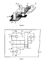
- the three-dimensional circuit shown in FIGS. 6 to 8 comprises, on a substrate 10 (not shown in the perspective view of FIG. 6), two superimposed levels, lower 11 and higher 12 respectively (FIG.
- the lower level 11 comprises transistors 13 of n-MOS type, formed in a first semiconductor layer. This is silicon having an orientation suitable for manufacturing n-MOS type transistors.
- the lower level is completed by a lower dielectric layer 14 (not shown in the perspective view of Figure 6), deposited on the transistors 13 and the substrate 10 and whose free face is flattened.
- the upper level 12 is disposed on the flattened free face of the lower dielectric layer 14. It comprises the p-MOS type transistors 15, formed in a second semiconductor layer and covered by an upper dielectric layer 16 (not shown in FIG. perspective view of Figure 6).
- the second semiconductor layer is made of germanium having a different orientation, suitable for the manufacture of p-MOS type transistors.
- the germanium layer is preferably pure germanium, but may optionally consist of highly concentrated germanium, for example an SiGe alloy comprising more than 80%, preferably more than 90%, of germanium.
- the physical properties, in particular the width of the band gap, of such an alloy are indeed comparable to those of pure germanium.
- the realization of the p-MOS transistors in the germanium layer can be carried out at a temperature of the order of 400 to 600 ° C., not affecting the n-MOS transistors 13, formed in the silicon at the lower level, more especially during manufacturing stages requiring a high temperature, such as the activation of dopants or the manufacture of the gate insulation.
- the choice of the stacking order of the transistors of the two levels is not random, but takes into account the maximum temperatures associated with the materials, in particular the semiconductor materials.
- the thermal budget for producing a MOS type transistor in germanium is less than approximately 600 ° C.
- the thermal budget for producing a MOS transistor in silicon is higher, generally higher than 800 ° C (typically of the order of 800 ° C to 1000 ° C).
- Transistors 13 of the lower level 11, which are of the n-MOS type, are preferably formed in a silicon orientation layer (100), whereas the higher level transistors 12, which are of type p MOS, are preferably made in an orientation germanium layer (110).
- At least one of the first and second semiconductor layers may have a constraint suitable for manufacturing the corresponding transistors.
- the silicon layer is preferably stress-stressed and the germanium layer in compression.
- the second semiconductor layer is preferably in biaxially constrained germanium. Germanium is preferably monocrystalline.
- the silicon layer, oriented (100), of the lower level 11 has a very good mobility for the electrons, while the germanium layer, oriented (110), of the upper level 12 offers excellent mobility for the holes .
- the semiconductor materials used are therefore optimal for both types of transistors.
- the optionally constrained silicon layer of the lower level 11 may be made by any suitable known method.
- this layer is formed on the silicon substrate 10 of orientation (100) by heteroepitaxy of a layer of relaxed SiGe, with a gradually increasing composition of germanium, until the desired composition is obtained. . Then a thin layer of silicon, less than the critical thickness (not relaxed) is formed by heteroepitaxy on the SiGe layer.
- the desired composition of the SiGe layer typically comprises of the order of 20 to 30% of germanium in silicon, which allows a significant increase in mobility in the constrained silicon layer, developed subsequently.
- the strained silicon layer is produced by transfer by the Smart Cut® process (implantation of hydrogen, bonding and detachment) of a surface layer containing the strained silicon layer and all or part of the SiGe layer on an SOI type structure, comprising a silicon substrate and an insulating layer.
- the SiGe layer is then removed by selective etching to leave only the silicon layer constrained.
- transistors 13, of n-MOS type are then conventionally made in the orientation silicon layer (100).
- This embodiment comprises the following successive steps: lateral isolation between transistors by etching and deposition of dielectrics, deposition of at least one gate dielectric, deposition and definition of patterns in a conductive material constituting the gate electrode G13, definition of spacers by dielectric deposition and dry etching, doping by ion implantation, activation of the dopants n of the source and the drain by annealing and production of silicides, for example NiSi.
- the dielectric 14 of the lower level 11 is then deposited on the substrate 10 and the transistors 13, then planarized, thus completing the manufacture of the lower level 11.
- a germanium orientation layer (110), derived from a substrate containing this material, is then transferred to the lower level 11, by molecular bonding and thinning or by the Smart Cut® process (implantation of hydrogen, bonding and detachment), as illustrated in FIG. 9.
- This type of substrate may be a monocrystalline germanium substrate of orientation (110), produced by conventional methods (for example Czochralski) or a silicon substrate.
- the germanium layer can also be obtained from a GeO1 substrate which is bonded and which is removed from the silicon support layer and the insulating layer (initially the buried oxide).
- This germanium layer may also be obtained by liquid phase epitaxy (LPE), in particular after opening a cavity opening on the substrate, in this case having an orientation (110) in order to obtain an oriented crystallization seed. followed by a step of cutting the germ.
- the transistors 15, of the p-MOS type are then conventionally produced in the germanium layer thus transferred on the lower level 11.
- This embodiment comprises, as previously, successively the lateral isolation between transistors by etching and deposition of dielectric, deposition of at least one gate dielectric, deposition and patterning in a conductive material constituting gate electrode G15, definition of spacers by dielectric deposition and dry etching, doping by ion implantation , activation of the dopants p of the source and of the drain by annealing and realization of the silicides.
- the use of a semiconductor layer of germanium, preferably monocrystalline allows the transistors 15 to be produced at temperatures as low as 400-600 ° C not affecting the transistors 13 already made at the lower level 11. These temperatures are, in particular, compatible with the stability of the silicides of the transistors of the lower level. Indeed, silicides currently used (NiSi) are stable up to about 600 ° C, by adding a few percent of Pt or Pd
- the dielectric 16 of the upper level 12 is then deposited on the dielectric 14 of the lower level 11 and on the transistors 15, and then possibly planarized, thus completing the fabrication of the upper level 12.
- first level of connections and interconnections of the circuit then begins with the etching and the metallization of vias through the different layers of the circuit.
- Simple vias V3 and V4, respectively associated with transistors 13 and 15, are etched through dielectrics 14 and / or 16 covering transistors 13 and 15, with stopping on the semiconductor layer of the corresponding transistor.
- Multiple vias V1 and V2 interconnect a lower level n-MOS transistor 13 to an associated higher level p-MOS transistor 15 to form a CMOS circuit.
- the vias are made by dry etching, preferably sequentially with several levels of lithography, so as to control the risks of overgrafting that may occur if one proceeds in a single step.
- the etching profile of the multiple vias V1 and V2, which respectively leave the drain or the source and the gate of the transistor 13 and successively pass through the dielectric 14, respectively the source or the drain and the gate of the associated transistor 15 and the dielectric 16, is preferably adapted to maximize the etching surface between the metal of the via and the material of the transistor. This can, for example, be achieved by a slight overgrading the dielectrics 14 and 16 with respect to the materials of the transistor 15 which are traversed by the via, as shown in Figure 10 for the via V1.
- the via V1 orifice is thus wider at the dielectrics 14 and 16 than at the semiconductor layer of the transistor 15 through which it passes.
- a second interconnection level is formed on the dielectric 16, for example to connect the vias V1 to V4, respectively to the output terminals S, input terminals E and the power supply terminals of the inverter or to other elements (not shown) of the circuit.
- the transistors 13 and 15 of the lower and upper levels are preferably arranged in such a way that the areas of these transistors intended to be interconnected overlap.
- the respective longitudinal axes A13 and A15 of a transistor 13 of the lower level and of a transistor 15 of the upper level respectively passing through the drain, the channel and the source of the transistor considered, are perpendicular.
- the transistors are asymmetrical, the drain or the source intended to be connected to the source or the drain of the associated transistor of the adjacent level being prolonged longitudinally, so as to form a first zone of recovery, in which is formed a first interconnection of the transistors of different levels, constituting the output S of the inverter.
- This first interconnection can then be constituted by a first vertical via V1.
- the gates G13 and G15 of the transistors are extended, perpendicular to their respective longitudinal axes, so as to form a second overlap zone at one of their ends.
- a second interconnection of the transistors of different levels, constituting the input E of the inverter can then be constituted by a second vertical via V2.
- Third and fourth vertical vias V3 and V4 are respectively formed at the ends of the transistors 13 and 15 opposite to the first overlap zone. These connections or simple vias can then serve as connections of the circuit, in particular to the supply terminals of the inverter.
- All the interconnections of the CMOS circuit are thus formed by means of vertical vias, directly interconnecting the connecting parts of two associated transistors of different levels and allowing their connection to other elements of the circuit. They can be formed at the same time as the single connections connecting a transistor to other circuit elements than the adjacent level complementary transistor.
- the vias can be made before making the germanium layer, which is easier to implement than after bonding. of Ge.
- each type of transistor N and P must be matched to the output work of the corresponding transistor.
- a first material is typically deposited to form first grids associated with one of the two types of transistors, then it is necessary to etch the material in order to form the second grids associated with the other type of transistors. This additional etching step is not necessary in the case of the three-dimensional technology according to the invention.
Landscapes
- Metal-Oxide And Bipolar Metal-Oxide Semiconductor Integrated Circuits (AREA)
Abstract
Description
- L'invention concerne un circuit intégré tridimensionnel de type CMOS formé dans un substrat hybride et comportant des transistors de types de conductivité différents, formés respectivement dans des première et seconde couches semi-conductrices disposées sur deux niveaux superposés, respectivement inférieur et supérieur.
- L'invention concerne également un procédé de fabrication d'un tel circuit.
- La recherche de rapidité dans les circuits intégrés de type C-MOS implique une diminution des temps de commutation des transistors ainsi que des temps de propagation dans les interconnexions du circuit.
- La diminution des temps de commutation peut être obtenue par une réduction de la longueur des canaux des transistors ainsi que par une augmentation de la mobilité des porteurs dans le semi-conducteur. L'augmentation de la mobilité des porteurs peut être obtenue par l'utilisation de deux couches de semi-conducteurs ayant chacun une mobilité améliorée, respectivement pour les électrons et pour les trous, à la place du silicium massif standard, d'orientation (100), non contraint, classiquement utilisé à la fois pour les transistors n-MOS et p-MOS du circuit. L'augmentation de la mobilité, pour les électrons dans les transistors n-MOS et pour les trous dans les transistors p-MOS, peut être obtenue par un choix d'orientation cristalline, la mise en contrainte des semi-conducteurs, un changement de matériau ou une combinaison de plusieurs de ces paramètres. Ainsi, une contrainte en tension dans le silicium améliore la mobilité des électrons, l'orientation de surface (110) procure une meilleure mobilité des trous mais une moins bonne mobilité des électrons que l'orientation (100), le germanium procure une meilleure mobilité des trous que le silicium, etc. Par ailleurs, les diélectriques de grille et les matériaux d'électrode de grille sont, de préférence, adaptés aux deux types de transistors, surtout si ceux-ci sont réalisés dans deux couches de natures, de contraintes ou d'orientations différentes.
- Il est ainsi connu d'utiliser pour la fabrication d'un circuit de type C-MOS un substrat hybride, c'est-à-dire un substrat sur lequel sont formées deux types de couches de semi-conducteur.
- Actuellement, il existe essentiellement trois méthodes de fabrication d'un substrat hybride.
- Une première méthode, illustrée aux figures 1 à 3, utilise l'hétéroépitaxie. Des couches épitaxiales 1 et 2, respectivement destinées à servir de base aux transistors n-MOS et p-MOS, sont formées successivement sur un substrat 3. Typiquement, on fait croître, sur un substrat 3 de silicium d'orientation (100), une première couche tampon d'alliage SiGe, par CVD, de composition graduellement croissante jusqu'à obtenir une couche de germanium pur relaxé en surface. Sur cette couche 1, on fait croître une fine couche 2 de silicium contraint. Après élimination sélective locale de la couche 2 de silicium contraint, les transistors p-MOS 4 sont formés dans la couche 1 de germanium et les transistors n-MOS 5 dans la couche 2 de silicium contraint. Des interconnexions 6 entre les transistors p-MOS et n-MOS, sont ensuite formées, par exemple comme représenté schématiquement sur la figure 3, entre le drain et la source des transistors p-MOS et n-MOS.
- Une seconde méthode, notamment décrite dans l'article "High Performance CMOS Fabricated on Hybrid Substrate With Different Crystal Orientations", de Yang et al., dans IEDM 03-453, p.18.7.1-18.7.2, et illustrée schématiquement à la figure 4, utilise le transfert de couche par collage moléculaire. Un substrat de silicium 7, d'orientation donnée, par exemple (110), est oxydé (couche isolante 8), puis transféré par la technologie Smart Cut® (implantation d'hydrogène, collage et détachement à l'emplacement de la ligne pointillée 9) sur un substrat de silicium 3 d'orientation différente, par exemple (100). La couche supérieure (substrat 7 sur isolant 8) amincie constitue ainsi une couche de silicium sur isolant (SOI), dans laquelle sont ultérieurement formés les transistors p-MOS. Cette couche est gravée pour exposer la surface du substrat 3 aux emplacements prévus pour les transistors n-MOS. On fait ensuite croître sélectivement, par homo-épitaxie localisée dans les orifices ainsi formés, du silicium d'orientation (100), dans lequel seront ultérieurement formés les transistors n-MOS. Dans l'article précité, les transistors n-MOS et p-MOS sont ainsi formés au même niveau, dans des substrats de silicium d'orientations différentes.
- Une troisième méthode, non représentée, utilise des déformations élastiques localisées. Les transistors n-MOS et p-MOS sont alors réalisés dans un même matériau (par exemple Si), dans des zones adjacentes, respectivement constituées par des couches de forte contrainte en tension et de forte contrainte en compression.
- Actuellement, la diminution du temps de propagation dans les interconnexions est essentiellement obtenue par une diminution de la résistivité des métaux (utilisation de cuivre) et/ou de la permittivité des diélectriques utilisés dans les interconnexions. La réduction de la permittivité des diélectriques implique une augmentation de leur porosité, provoquant une forte dégradation de leurs propriétés mécaniques et thermiques. Il est donc difficile d'aller au-delà dans cette voie.
- Une diminution du temps de propagation dans les interconnexions a également été obtenue par une intégration tridimensionnelle (intégration 3D) des circuits, les transistors étant empilés les uns sur les autres.
- La demande de brevet
US 2004/0145399 décrit un circuit CMOS tridimensionnel constitué par la superposition d'un transistor p-MOS sur un transistor n-MOS (ou inversement). La couche de semi-conducteur supérieure est formée par épitaxie localisée en utilisant comme germe un via semi-conducteur, lui-même formé par croissance épitaxiale du semi-conducteur inférieur. La source et le drain du transistor n-MOS sont verticalement alignés respectivement avec la source et le drain du transistor p-MOS. Il en va de même de leurs grilles. Des interconnexions sont prévues, notamment pour connecter les deux transistors de la manière représentée à la figure 5, pour former un inverseur. Les deux transistors sont ainsi connectés en série entre une borne d'alimentation et la masse, le point commun aux deux transistors en série constituant la sortie S de l'inverseur, et leurs grilles sont connectées à l'entrée E de l'inverseur. - Dans le mode de réalisation décrit dans l'article "3-D ICs : A Novel Chip Design for Improving Deep-Submicrometer Interconnect Performance and Systems-on-Chip Integration", de Banerjee et al., dans Proceedings of the IEEE, vol.89, n°5, p. 602-630, de mai 2001, des transistors ou des blocs de circuits complets, incluant leurs métallisations et une partie des interconnexions, sont réalisés séparément sur au moins deux substrats. Les blocs sont ensuite alignés et collés les uns au-dessus des autres. L'un des substrats est éliminé et les différents niveaux sont interconnectés par des techniques connues de métallisation en surface. La densité de connexion d'un niveau à l'autre est notamment limitée par les technologies d'alignement actuellement disponibles (au mieux de l'ordre de 1 à 2µm).
- L'article "Three-Dimensional Metal Gate-High-K-GOI CMOSFETS on 1-Poly-6-Metal 0.18µm Si Devices", de YU et al., dans IEEE Electron Device Letters, vol.26, n°2, p.118-120, de février 2005, décrit une intégration 3D de CMOS formés dans une couche de germanium sur isolant (GeOI) et de CMOS formés dans du silicium. La superposition est réalisée par report par la technologie Smart Cut® (implantation d'hydrogène, collage et détachement) d'une couche de germanium au-dessus de multicouches d'interconnexions en cuivre des circuits CMOS préalablement réalisés dans le silicium, au premier niveau. Des circuits CMOS sont ensuite formés dans le germanium, au second niveau, sans affecter les structures sous-jacentes.
- L'invention a pour but un circuit tridimensionnel ne présentant pas les inconvénients des circuits connus, ainsi que son procédé de fabrication. Plus particulièrement, l'invention a pour but d'optimiser la fabrication d'un tel circuit.
- Selon l'invention, ce but est atteint par un circuit selon les revendications annexées et plus particulièrement par le fait que les transistors de type n-MOS sont formés, au niveau inférieur, dans la première couche semi-conductrice, en silicium d'orientation (100), les transistors de type p-MOS étant formés, au niveau supérieur, dans la seconde couche semi-conductrice, en germanium d'orientation (110).
- Un procédé de fabrication d'un tel circuit est caractérisé par le fait qu'il comporte successivement :
- la fabrication d'un premier bloc comportant les transistors de type n-MOS formés dans une couche semi-conductrice en silicium ayant une orientation adaptée à la fabrication de transistors de type n-MOS,
- le transfert sur le premier bloc d'une couche semi-conductrice en germanium ayant une orientation adaptée à la fabrication de transistors de type p-MOS et
- la fabrication des transistors de type p-MOS dans la couche semi-conductrice en germanium, à une température n'affectant pas les transistors formés dans la couche semi-conductrice en silicium.
- D'autres avantages et caractéristiques ressortiront plus clairement de la description qui va suivre de modes particuliers de réalisation de l'invention donnés à titre d'exemples non limitatifs et représentés aux dessins annexés, dans lesquels :
- Les figures 1 à 3 illustrent la réalisation d'un substrat hybride selon l'art antérieur par hétéroépitaxie.
- La figure 4 illustre la formation d'un substrat hybride selon l'art antérieur par transfert de couche.
- La figure 5 représente le schéma électrique classique d'un inverseur constitué par des transistors p-MOS et n-MOS.
- Les figures 6 à 8 illustrent un mode de réalisation particulier d'un circuit selon l'invention, respectivement en perspective, en vue de dessus et en coupe selon A-A.
- La figure 9 illustre un mode particulier de fabrication d'un circuit selon l'invention.
- La figure 10 illustre schématiquement un mode particulier de réalisation d'un via multiple d'un circuit selon l'invention.
- Le circuit tridimensionnel représenté aux figures 6 à 8, comporte, sur un substrat 10 (non représenté dans la vue en perspective de la figure 6), deux niveaux superposés, respectivement inférieur 11 et supérieur 12 (fig.8).
- Le niveau inférieur 11 comporte les transistors 13 de type n-MOS, formés dans une première couche semi-conductrice. Celle-ci est en silicium ayant une orientation adaptée à la fabrication de transistors de type n-MOS. Le niveau inférieur est complété par une couche diélectrique inférieure 14 (non représentée dans la vue en perspective de la figure 6), déposée sur les transistors 13 et le substrat 10 et dont la face libre est aplanie.
- Le niveau supérieur 12 est disposé sur la face libre aplanie de la couche diélectrique inférieure 14. Il comporte les transistors 15 de type p-MOS, formés dans une seconde couche semi-conductrice et recouverts par une couche diélectrique supérieure 16 (non représentée dans la vue en perspective de la figure 6). La seconde couche semi-conductrice est en germanium ayant une orientation différente, adaptée à la fabrication de transistors de type p-MOS. La couche en germanium est, de préférence, en germanium pur, mais peut éventuellement être constituée par du germanium très concentré, par exemple par un alliage SiGe comportant plus de 80%, de préférence plus de 90%, de germanium. Les propriétés physiques, notamment la largeur de la bande interdite, d'un tel alliage sont en effet comparables à celles du germanium pur.
- La réalisation des transistors p-MOS dans la couche de germanium peut se faire à une température de l'ordre de 400 à 600°C, n'affectant pas les transistors n-MOS 13, formés dans le silicium au niveau inférieur, plus particulièrement lors des étapes de fabrication nécessitant une forte température, comme l'activation des dopants ou la fabrication de l'isolant de grille.
- Le choix de l'ordre d'empilement des transistors des deux niveaux n'est pas aléatoire, mais tient compte des températures maximales associées aux matériaux, notamment aux matériaux semi-conducteurs. En effet, le budget thermique de réalisation d'un transistor de type MOS dans le germanium est inférieur à environ 600°C, tandis que le budget thermique de réalisation d'un transistor de type MOS dans le silicium est plus élevé, généralement supérieur à 800°C (typiquement de l'ordre de 800°C à 1000°C).
- Les transistors 13 du niveau inférieur 11, qui sont de type n-MOS, sont, de préférence, formés dans une couche de silicium d'orientation (100), tandis que les transistors 15 du niveau supérieur 12, qui sont de type p-MOS, sont, de préférence, réalisés dans une couche de germanium d'orientation (110).
- Au moins l'une des première et seconde couches semi-conductrices peut avoir une contrainte adaptée à la fabrication des transistors correspondants. Ainsi, la couche de silicium est, de préférence, contrainte en tension et la couche de germanium en compression. La seconde couche semi-conductrice est, de préférence, en germanium contraint biaxialement. Le germanium est, de préférence, monocristallin.
- La couche de silicium, d'orientation (100), du niveau inférieur 11 possède une très bonne mobilité pour les électrons, tandis que la couche en germanium, d'orientation (110), du niveau supérieur 12 offre une excellente mobilité pour les trous. Les matériaux semi-conducteurs utilisés sont donc optimums pour les deux types de transistors.
- La couche de silicium, éventuellement contraint, du niveau inférieur 11 peut être réalisée par tout procédé connu approprié.
- Dans une première variante de réalisation, cette couche est formée sur le substrat 10 en silicium, d'orientation (100), par hétéroépitaxie d'une couche de SiGe relaxée, de composition graduellement croissante en germanium, jusqu'à obtention de la composition désirée. Puis une fine couche de silicium, d'épaisseur inférieure à l'épaisseur critique (non relaxé) est formée par hétéroépitaxie sur la couche en SiGe. La composition désirée de la couche de SiGe comporte typiquement de l'ordre de 20 à 30% de germanium dans le silicium, ce qui permet une augmentation importante de la mobilité dans la couche de silicium contraint, élaborée ensuite.
- Dans une seconde variante de réalisation, la couche de silicium contraint est réalisée par transfert par le procédé Smart Cut® (implantation d'hydrogène, collage et détachement) d'une couche de surface contenant la couche de silicium contraint et tout ou partie de la couche SiGe sur une structure de type SOI, comportant un substrat de silicium et une couche isolante. La couche de SiGe est alors éliminée par attaque chimique sélective pour ne laisser que la couche de silicium contraint.
- Dans les deux variantes, les transistors 13, de type n-MOS, sont ensuite réalisés, de manière classique, dans la couche de silicium d'orientation (100). Cette réalisation comporte les étapes successives suivantes : isolation latérale entre transistors par gravure et dépôt de diélectriques, dépôt d'au moins un diélectrique de grille, dépôt et définition de motifs dans un matériau conducteur constituant l'électrode de grille G13, définition d'espaceurs par dépôt de diélectrique et gravure sèche, dopage par implantation ionique, activation des dopants n de la source et du drain par recuit et réalisation des siliciures, par exemple en NiSi. Le diélectrique 14 du niveau inférieur 11 est ensuite déposé sur le substrat 10 et les transistors 13, puis planarisé, terminant ainsi la fabrication du niveau inférieur 11.
- Dans un mode de réalisation préférentiel, une couche de germanium d'orientation (110), issue d'un substrat contenant ce matériau, est ensuite transférée sur le niveau inférieur 11, par collage moléculaire et amincissement ou par le procédé Smart Cut® (implantation d'hydrogène, collage et détachement), comme illustré à la figure 9. Ce type de substrat peut être un substrat monocristallin de germanium, d'orientation (110), élaboré par les procédés classiques (par exemple Czochralski) ou un substrat de silicium d'orientation (110) sur lequel on a fait croître une première couche relaxée (sans contrainte), dite couche tampon, d'alliage SiGe de concentration graduellement croissante en germanium, puis une couche de germanium pur. La couche de germanium peut aussi être obtenue à partir d'un substrat GeOl que l'on colle et dont on supprime la couche support en silicium ainsi que la couche isolante (initialement l'oxyde enterré). On peut aussi obtenir cette couche de germanium par épitaxie en phase liquide (LPE : Liquid Phase Epitaxy), notamment après ouverture d'une cavité débouchant sur le substrat ayant dans ce cas une orientation (110) afin d'obtenir un germe de cristallisation orienté, suivie d'une étape de coupure du germe.
- Les transistors 15, de type p-MOS, sont ensuite réalisés, de manière classique, dans la couche de germanium ainsi transférée sur le niveau inférieur 11. Cette réalisation comporte, comme précédemment, successivement l'isolation latérale entre transistors par gravure et dépôt de diélectriques, le dépôt d'au moins un diélectrique de grille, le dépôt et la définition de motifs dans un matériau conducteur constituant l'électrode de grille G15, la définition d'espaceurs par dépôt de diélectrique et gravure sèche, le dopage par implantation ionique, activation des dopants p de la source et du drain par recuit et réalisation des siliciures. L'utilisation d'une couche semi-conductrice en germanium, de préférence monocristallin, permet de réaliser les transistors 15 à des températures aussi faibles que 400-600°C n'affectant pas les transistors 13 déjà réalisés au niveau inférieur 11. Ces températures sont, en particulier, compatibles avec la stabilité des siliciures des transistors du niveau inférieur. En effet, les siliciures actuellement utilisés (NiSi) sont stables jusqu'à environ 600°C, par adjonction de quelques pourcents de Pt ou Pd.
- Comme représenté à la figure 8, le diélectrique 16 du niveau supérieur 12 est ensuite déposé sur le diélectrique 14 du niveau inférieur 11 et sur les transistors 15, puis éventuellement planarisé, terminant ainsi la fabrication du niveau supérieur 12.
- La réalisation d'un premier niveau de connexions et d'interconnexions du circuit commence ensuite par la gravure et la métallisation de vias à travers les différentes couches du circuit. Des vias simples V3 et V4, respectivement associé aux transistors 13 et 15, sont gravés à travers les diélectriques 14 et/ou 16 recouvrant les transistors 13 et 15, avec arrêt sur la couche semi-conductrice du transistor correspondant. Des vias multiples V1 et V2 interconnectent un transistor n-MOS 13 du niveau inférieur à un transistor p-MOS 15 associé du niveau supérieur pour former un circuit CMOS.
- Les vias sont réalisés par gravure sèche, de préférence séquentiellement avec plusieurs niveaux de lithographie, de manière à contrôler les risques de surgravure susceptibles d'apparaître si l'on procède en une seule étape. Le profil de gravure des vias multiples V1 et V2, qui partent respectivement du drain ou de la source et de la grille du transistor 13 et traversent successivement le diélectrique 14, respectivement la source ou le drain et la grille du transistor 15 associé et le diélectrique 16, est, de préférence adapté de manière à maximiser la surface de gravure entre le métal du via et le matériau du transistor. Ceci peut, par exemple, être réalisé par une légère surgravure des diélectriques 14 et 16 par rapport aux matériaux du transistor 15 qui sont traversés par le via, comme représenté à la figure 10 pour le via V1. L'orifice du via V1 est ainsi plus large au niveau des diélectriques 14 et 16 qu'au niveau de la couche semi-conductrice du transistor 15 qu'il traverse.
- Comme représenté à la figure 10, un second niveau d'interconnexion est formé sur le diélectrique 16, par exemple pour connecter les vias V1 à V4, respectivement aux bornes de sortie S, d'entrée E et d'alimentation de l'inverseur ou à d'autres éléments (non représentés) du circuit.
- Le procédé de fabrication selon l'invention comporte ainsi successivement au moins:
- la fabrication d'un premier bloc comportant les transistors (13) de type n-MOS formés dans une couche semi-conductrice en silicium ayant une orientation adaptée à la fabrication de transistors (13) de type n-MOS,
- le transfert sur le premier bloc d'une couche semi-conductrice en germanium ayant une orientation adaptée à la fabrication de transistors (15) de type p-MOS et
- la fabrication des transistors (15) de type p-MOS dans la couche semi-conductrice en germanium, à une température n'affectant pas les transistors formés dans la couche semi-conductrice en silicium.
- Dans le mode particulier de réalisation décrit ci-dessus, le procédé de fabrication comporte successivement :
- la fabrication des transistors 13, de type n-MOS, du premier niveau ou niveau inférieur 11, dans une couche en silicium contraint en tension, d'orientation (100),
- le dépôt et la planarisation d'une couche diélectrique 14, au premier niveau,
- la formation de la seconde couche semi-conductrice, en germanium monocristallin d'orientation (110), contraint en compression,
- la fabrication des transistors 15, de type p-MOS, du second niveau ou niveau supérieur 12,
- le dépôt d'une seconde couche diélectrique 16, au second niveau,
- la formation de vias multiples verticaux (V1, V2), constituant les interconnexions entre les transistors (13, 15) de niveaux différents, et de vias simples verticaux (V3, V4), constituant diverses connexions du circuit.
- Les transistors 13 et 15 des niveaux inférieur et supérieur sont, de préférence, disposés de manière à ce que les zones de ces transistors destinées à être interconnectées se recouvrent. Ainsi, par exemple, sur les figures 6 à 8, pour fabriquer un inverseur selon la figure 5, les axes longitudinaux respectifs A13 et A15 d'un transistor 13 du niveau inférieur et d'un transistor 15 du niveau supérieur, passant respectivement par le drain, le canal et la source du transistor considéré, sont perpendiculaires.
- Dans certains cas, notamment pour résoudre des problèmes de connectique, les transistors sont asymétriques, le drain ou la source destinée à être connectée à la source ou au drain du transistor associé du niveau adjacent étant prolongé longitudinalement, de manière à former une première zone de recouvrement, dans laquelle est formée une première interconnexion des transistors de niveaux différents, constituant la sortie S de l'inverseur. Cette première interconnexion peut alors être constituée par un premier via vertical V1. Simultanément, les grilles G13 et G15 des transistors, classiquement formées au-dessus du canal correspondant, sont prolongées, perpendiculairement à leurs axes longitudinaux respectifs, de manière à former une seconde zone de recouvrement à une de leurs extrémités. Une seconde interconnexion des transistors de niveaux différents, constituant l'entrée E de l'inverseur, peut alors être constituée par un second via vertical V2. Ces interconnexions ou vias multiples connectent ainsi directement un transistor avec le transistor complémentaire associé du niveau adjacent.
- Des troisième et quatrième vias verticaux V3 et V4 sont respectivement formés aux extrémités des transistors 13 et 15 opposés à la première zone de recouvrement. Ces connexions ou vias simples peuvent alors servir de connexions du circuit, notamment aux bornes d'alimentation de l'inverseur.
- Toutes les interconnexions du circuit CMOS sont ainsi réalisées par l'intermédiaire de vias verticaux, interconnectant directement les parties à connecter de deux transistors associés de niveaux différents et permettant leur connexion à d'autres éléments du circuit. Elles peuvent être formées en même temps que les connexions simples connectant un transistor à d'autres éléments du circuit que le transistor complémentaire de niveau adjacent.
- Cette disposition particulière des transistors complémentaires associés des deux niveaux superposés permet d'obtenir un assemblage 3D très dense, avec une densification du nombre de transistors par unité de surface et une diminution de la longueur moyenne des connexions.
- Les températures utilisées lors de la fabrication de la couche semi-conductrice en germanium étant inférieures à 700°C, les vias peuvent être réalisées avant de réaliser la couche de germanium, ce qui est notamment plus facile à mettre en oeuvre qu'après le collage du Ge.
- Le matériau d'électrode de grille de chaque type de transistor (N et P) doit être adapté au travail de sortie du transistor correspondant. Dans le cas d'une technologie planaire, on dépose typiquement un premier matériau pour former des premières grilles associées à l'un des deux types de transistors, puis il est nécessaire de graver le matériau pour pouvoir former les secondes grilles associées à l'autre type de transistors. Cette étape de gravure supplémentaire n'est pas nécessaire dans le cas de la technologie tridimensionnelle selon l'invention.
Claims (19)
- Circuit intégré tridimensionnel de type CMOS formé dans un substrat hybride et comportant des transistors de types de conductivité différents, formés respectivement dans des première et seconde couches semi-conductrices disposées sur deux niveaux superposés, respectivement inférieur et supérieur, circuit caractérisé en ce que les transistors (13) de type n-MOS sont formés, au niveau inférieur, dans la première couche semi-conductrice, en silicium d'orientation (100), les transistors (15) de type p-MOS étant formés, au niveau supérieur, dans la seconde couche semi-conductrice, en germanium d'orientation (110).
- Circuit selon la revendication 1, caractérisé en ce qu'au moins l'une des première et seconde couches semi-conductrices a une contrainte adaptée à la fabrication des transistors correspondants.
- Circuit selon la revendication 2, caractérisé en ce que la première couche semi-conductrice est en silicium contraint en tension.
- Circuit selon l'une des revendications 2 et 3, caractérisé en ce que la seconde couche semi-conductrice est en germanium contraint en compression.
- Circuit selon la revendication 4, caractérisé en ce que la seconde couche semi-conductrice est en germanium contraint biaxialement.
- Circuit selon l'une quelconque des revendications 1 à 5, caractérisé en ce que le germanium est monocristallin.
- Circuit selon l'une quelconque des revendications 1 à 6, caractérisé en ce que les axes longitudinaux (A13, A15) d'un transistor (13) de type n-MOS et d'un transistor (15) de type p-MOS associé sont perpendiculaires, de manière à former au moins une zone de recouvrement, dans laquelle est formée une interconnexion (V1, V2) desdits transistors associés.
- Circuit selon la revendication 7, caractérisé en ce que le drain ou la source d'un transistor (13) de type n-MOS étant destinée à être connecté à la source ou au drain d'un transistor (15) de type n-MOS associé, ils sont prolongés longitudinalement, de manière à former une première zone de recouvrement, dans laquelle est formée une première interconnexion (V1) des transistors.
- Circuit selon la revendication 8, caractérisé en ce qu'il comporte des connexions verticales (V3, V4) formées aux extrémités des transistors (13, 15) opposées à la première zone de recouvrement.
- Circuit selon l'une quelconque des revendications 7 à 9, caractérisé en ce que les grilles (G13, G15) des transistors (13, 15) sont prolongées, perpendiculairement à leurs axes longitudinaux respectifs (A13, A15), de manière à former, à une de leurs extrémités, une seconde zone de recouvrement, dans laquelle est formée une seconde interconnexion (V2) des transistors.
- Procédé de fabrication d'un circuit intégré tridimensionnel de type CMOS formé dans un substrat hybride et comportant des transistors de types de conductivité différents, formés respectivement dans des première et seconde couches semi-conductrices superposées, procédé caractérisé en ce qu'il comporte successivement:- la fabrication d'un premier bloc comportant les transistors (13) de type n-MOS formés dans une couche semi-conductrice en silicium ayant une orientation adaptée à la fabrication de transistors (13) de type n-MOS,- le transfert sur le premier bloc d'une couche semi-conductrice en germanium ayant une orientation adaptée à la fabrication de transistors (15) de type p-MOS et- la fabrication des transistors (15) de type p-MOS dans la couche semi-conductrice en germanium, à une température n'affectant pas les transistors formés dans la couche semi-conductrice en silicium.
- Procédé selon la revendication 11, caractérisé en ce que la température de fabrication des transistors (15) de type p-MOS dans la couche semi-conductrice en germanium est de l'ordre de 400 à 600°C.
- Procédé selon l'une des revendications 11 et 12, caractérisé en ce que le transfert de la couche semi-conductrice en germanium sur le premier bloc est réalisé par collage moléculaire et amincissement.
- Procédé selon l'une des revendications 11 et 12, caractérisé en ce que le transfert de la couche semi-conductrice en germanium sur le premier bloc est réalisé par report par implantation d'hydrogène, collage et détachement.
- Procédé selon l'une des revendications 11 et 12, caractérisé en ce que le transfert de la couche semi-conductrice en germanium sur le premier bloc est réalisé par épitaxie en phase liquide après ouverture d'une cavité débouchant sur le substrat ayant une orientation (110) afin d'obtenir un germe de cristallisation orienté.
- Procédé selon l'une quelconque des revendications 11 à 15, caractérisé en ce qu'il comporte la formation de vias multiples (V1, V2) verticaux, constituant les interconnexions entre les transistors associés de type n-MOS (13) et de type p-MOS (15) de niveaux différents.
- Procédé selon l'une quelconque des revendications 11 à 16, caractérisé en ce qu'il comporte la formation de vias simples (V3, V4) verticaux, constituant diverses connexions du circuit.
- Procédé selon l'une quelconque des revendications 11 à 17, caractérisé en ce qu'il comporte la formation de vias avant la réalisation de la couche semi-conductrice en germanium.
- Procédé selon l'une des revendications 11 à 18, caractérisé en ce que le silicium de la première couche conductrice a une orientation (100) et le germanium de la seconde couche conductrice une orientation (110).
Applications Claiming Priority (1)
| Application Number | Priority Date | Filing Date | Title |
|---|---|---|---|
| FR0600577A FR2896620B1 (fr) | 2006-01-23 | 2006-01-23 | Circuit integre tridimensionnel de type c-mos et procede de fabrication |
Publications (3)
| Publication Number | Publication Date |
|---|---|
| EP1811567A2 true EP1811567A2 (fr) | 2007-07-25 |
| EP1811567A3 EP1811567A3 (fr) | 2013-12-25 |
| EP1811567B1 EP1811567B1 (fr) | 2015-12-23 |
Family
ID=36930147
Family Applications (1)
| Application Number | Title | Priority Date | Filing Date |
|---|---|---|---|
| EP07354005.6A Active EP1811567B1 (fr) | 2006-01-23 | 2007-01-19 | Circuit intégré tridimensionnel de type C-MOS et procédé de fabrication |
Country Status (3)
| Country | Link |
|---|---|
| US (1) | US7763915B2 (fr) |
| EP (1) | EP1811567B1 (fr) |
| FR (1) | FR2896620B1 (fr) |
Families Citing this family (12)
| Publication number | Priority date | Publication date | Assignee | Title |
|---|---|---|---|---|
| US8288756B2 (en) * | 2007-11-30 | 2012-10-16 | Advanced Micro Devices, Inc. | Hetero-structured, inverted-T field effect transistor |
| FR2935539B1 (fr) * | 2008-08-26 | 2010-12-10 | Commissariat Energie Atomique | Circuit cmos tridimensionnel sur deux substrats desalignes et procede de realisation |
| FR2938376B1 (fr) | 2008-11-07 | 2010-12-31 | Commissariat Energie Atomique | Procede de preparation d'une couche de monosiliciure de nickel nisi sur un substrat en silicium |
| FR2979481B1 (fr) | 2011-08-25 | 2016-07-01 | Commissariat Energie Atomique | Procede de realisation d'un circuit integre tridimensionnel |
| US9257407B2 (en) * | 2013-10-28 | 2016-02-09 | Qualcomm Incorporated | Heterogeneous channel material integration into wafer |
| FR3031835B1 (fr) | 2015-01-16 | 2017-12-22 | Commissariat Energie Atomique | Procede de realisation d'un circuit electronique integre tridimensionnel |
| US10361219B2 (en) | 2015-06-30 | 2019-07-23 | International Business Machines Corporation | Implementing a hybrid finFET device and nanowire device utilizing selective SGOI |
| US9502420B1 (en) * | 2015-12-19 | 2016-11-22 | International Business Machines Corporation | Structure and method for highly strained germanium channel fins for high mobility pFINFETs |
| US20200212038A1 (en) * | 2018-12-28 | 2020-07-02 | Intel Corporation | Self-aligned stacked ge/si cmos transistor structure |
| US12308370B2 (en) * | 2021-09-29 | 2025-05-20 | Advanced Micro Devices, Inc. | Cross field effect transistors (XFETs) in integrated circuits |
| US11862640B2 (en) | 2021-09-29 | 2024-01-02 | Advanced Micro Devices, Inc. | Cross field effect transistor (XFET) library architecture power routing |
| US12009326B2 (en) | 2022-01-26 | 2024-06-11 | Globalfoundries Singapore Pte. Ltd. | SRAM bit cells with three-dimensional integration |
Family Cites Families (10)
| Publication number | Priority date | Publication date | Assignee | Title |
|---|---|---|---|---|
| US6882010B2 (en) | 2002-10-03 | 2005-04-19 | Micron Technology, Inc. | High performance three-dimensional TFT-based CMOS inverters, and computer systems utilizing such novel CMOS inverters |
| US6998683B2 (en) * | 2002-10-03 | 2006-02-14 | Micron Technology, Inc. | TFT-based common gate CMOS inverters, and computer systems utilizing novel CMOS inverters |
| US6900667B2 (en) * | 2003-03-11 | 2005-05-31 | Micron Technology, Inc. | Logic constructions and electronic devices |
| US6902962B2 (en) * | 2003-04-04 | 2005-06-07 | Taiwan Semiconductor Manufacturing Company, Ltd. | Silicon-on-insulator chip with multiple crystal orientations |
| US7208815B2 (en) * | 2004-05-28 | 2007-04-24 | Taiwan Semiconductor Manufacturing Company, Ltd. | CMOS logic gate fabricated on hybrid crystal orientations and method of forming thereof |
| US7187059B2 (en) * | 2004-06-24 | 2007-03-06 | International Business Machines Corporation | Compressive SiGe <110> growth and structure of MOSFET devices |
| US7298009B2 (en) * | 2005-02-01 | 2007-11-20 | Infineon Technologies Ag | Semiconductor method and device with mixed orientation substrate |
| US7432149B2 (en) * | 2005-06-23 | 2008-10-07 | Taiwan Semiconductor Manufacturing Company, Ltd. | CMOS on SOI substrates with hybrid crystal orientations |
| US7524707B2 (en) * | 2005-08-23 | 2009-04-28 | Freescale Semiconductor, Inc. | Modified hybrid orientation technology |
| US20070145367A1 (en) * | 2005-12-27 | 2007-06-28 | Taiwan Semiconductor Manufacturing Company, Ltd. | Three-dimensional integrated circuit structure |
-
2006
- 2006-01-23 FR FR0600577A patent/FR2896620B1/fr not_active Expired - Fee Related
-
2007
- 2007-01-18 US US11/654,660 patent/US7763915B2/en active Active
- 2007-01-19 EP EP07354005.6A patent/EP1811567B1/fr active Active
Also Published As
| Publication number | Publication date |
|---|---|
| FR2896620B1 (fr) | 2008-05-30 |
| EP1811567B1 (fr) | 2015-12-23 |
| EP1811567A3 (fr) | 2013-12-25 |
| US20070170471A1 (en) | 2007-07-26 |
| FR2896620A1 (fr) | 2007-07-27 |
| US7763915B2 (en) | 2010-07-27 |
Similar Documents
| Publication | Publication Date | Title |
|---|---|---|
| EP1811567B1 (fr) | Circuit intégré tridimensionnel de type C-MOS et procédé de fabrication | |
| EP2075826B1 (fr) | Procédé de fabrication d'un substrat semiconducteur-sur-isolant comprenant une étape d'enrichissement en Ge localisé | |
| EP1095407B1 (fr) | Circuit integre de type soi a capacite de decouplage, et procede de realisation d'un tel circuit | |
| EP2562802B1 (fr) | Procede de realisation d'un circuit integre tridimensionnel | |
| EP3847693B1 (fr) | Procede de fabrication d'un dispositif cfet | |
| TWI552338B (zh) | 異質層裝置 | |
| EP2293327A1 (fr) | Circuit intégré à transistors MOS couplés électrostatiquement et procédé de réalisation d'un tel circuit intégré | |
| EP2869342B1 (fr) | Procédé de fabrication d'un dispositif comprenant un circuit intégré et des cellules photovoltaïques et dispositif | |
| FR2649831A1 (fr) | Dispositif soi-mos presentant une structure de paroi laterale conductrice et procede pour sa fabrication | |
| FR3118828A1 (fr) | Procédé de collage direct de substrats | |
| FR2928029A1 (fr) | Procede de fabrication d'un dispositif semi-conducteur a grille enterree et circuit integre correspondant. | |
| FR2693314A1 (fr) | Transistor JFET vertical à mode de fonctionnement bipolaire optimisé et procédé de fabrication correspondant. | |
| EP1808890A1 (fr) | Procédé de réalisation d'une couche monocristalline sur une couche diélectrique | |
| FR2896338A1 (fr) | Procede de realisation d'une couche monocristalline sur une couche dielectrique | |
| FR2915318A1 (fr) | Procede de realisation d'un circuit electronique integre a deux portions de couches actives ayant des orientations cristallines differentes | |
| FR2910456A1 (fr) | Procede de realisation de microfils et/ou de nanofils | |
| FR2910704A1 (fr) | Procede de realisation d'un dispositif a circuit integre interconnecte | |
| TWI593125B (zh) | 平面式異質裝置及其製造方法 | |
| EP1223614A1 (fr) | Procédé de fabrication d'un substrat monocristallin, et circuit intégré comportant un tel substrat | |
| KR101841359B1 (ko) | 모놀리틱 3차원 반도체 구조물 및 이의 제조방법 | |
| WO2025108891A1 (fr) | Super reseaux doubles obtenus par transfert de couche, structure et procede de fabrication | |
| WO2025108884A1 (fr) | Procede de fabrication de super reseaux doubles obtenus par transfert de couche | |
| WO2025108893A1 (fr) | Super réseau obtenu par transfert de couche, structure et procédé de fabrication | |
| CN101409297B (zh) | 三维量子阱nmos集成器件及其制作方法 | |
| EP4145491A1 (fr) | Procédé de fabrication d'un circuit intégré |
Legal Events
| Date | Code | Title | Description |
|---|---|---|---|
| PUAI | Public reference made under article 153(3) epc to a published international application that has entered the european phase |
Free format text: ORIGINAL CODE: 0009012 |
|
| AK | Designated contracting states |
Kind code of ref document: A2 Designated state(s): AT BE BG CH CY CZ DE DK EE ES FI FR GB GR HU IE IS IT LI LT LU LV MC NL PL PT RO SE SI SK TR |
|
| AX | Request for extension of the european patent |
Extension state: AL BA HR MK YU |
|
| RAP1 | Party data changed (applicant data changed or rights of an application transferred) |
Owner name: COMMISSARIAT A L'ENERGIE ATOMIQUE ET AUX ENERGIES |
|
| PUAL | Search report despatched |
Free format text: ORIGINAL CODE: 0009013 |
|
| AK | Designated contracting states |
Kind code of ref document: A3 Designated state(s): AT BE BG CH CY CZ DE DK EE ES FI FR GB GR HU IE IS IT LI LT LU LV MC NL PL PT RO SE SI SK TR |
|
| AX | Request for extension of the european patent |
Extension state: AL BA HR MK RS |
|
| RIC1 | Information provided on ipc code assigned before grant |
Ipc: H01L 27/06 20060101AFI20131121BHEP |
|
| 17P | Request for examination filed |
Effective date: 20140623 |
|
| RBV | Designated contracting states (corrected) |
Designated state(s): AT BE BG CH CY CZ DE DK EE ES FI FR GB GR HU IE IS IT LI LT LU LV MC NL PL PT RO SE SI SK TR |
|
| AKX | Designation fees paid |
Designated state(s): DE FR |
|
| GRAP | Despatch of communication of intention to grant a patent |
Free format text: ORIGINAL CODE: EPIDOSNIGR1 |
|
| INTG | Intention to grant announced |
Effective date: 20150721 |
|
| RIN1 | Information on inventor provided before grant (corrected) |
Inventor name: FAYNOT, OLIVIER Inventor name: JOLY, JEAN-PIERRE Inventor name: CLAVELIER, LAURENT |
|
| GRAS | Grant fee paid |
Free format text: ORIGINAL CODE: EPIDOSNIGR3 |
|
| GRAA | (expected) grant |
Free format text: ORIGINAL CODE: 0009210 |
|
| AK | Designated contracting states |
Kind code of ref document: B1 Designated state(s): DE FR |
|
| REG | Reference to a national code |
Ref country code: FR Ref legal event code: PLFP Year of fee payment: 10 |
|
| REG | Reference to a national code |
Ref country code: DE Ref legal event code: R096 Ref document number: 602007044268 Country of ref document: DE |
|
| REG | Reference to a national code |
Ref country code: DE Ref legal event code: R097 Ref document number: 602007044268 Country of ref document: DE |
|
| PLBE | No opposition filed within time limit |
Free format text: ORIGINAL CODE: 0009261 |
|
| STAA | Information on the status of an ep patent application or granted ep patent |
Free format text: STATUS: NO OPPOSITION FILED WITHIN TIME LIMIT |
|
| 26N | No opposition filed |
Effective date: 20160926 |
|
| REG | Reference to a national code |
Ref country code: FR Ref legal event code: PLFP Year of fee payment: 11 |
|
| REG | Reference to a national code |
Ref country code: FR Ref legal event code: PLFP Year of fee payment: 12 |
|
| REG | Reference to a national code |
Ref country code: DE Ref legal event code: R079 Ref document number: 602007044268 Country of ref document: DE Free format text: PREVIOUS MAIN CLASS: H01L0027060000 Ipc: H10D0084000000 |
|
| PGFP | Annual fee paid to national office [announced via postgrant information from national office to epo] |
Ref country code: DE Payment date: 20250120 Year of fee payment: 19 |
|
| PGFP | Annual fee paid to national office [announced via postgrant information from national office to epo] |
Ref country code: FR Payment date: 20250122 Year of fee payment: 19 |