EP1808860A1 - Testing storage system electronics using loopback - Google Patents
Testing storage system electronics using loopback Download PDFInfo
- Publication number
- EP1808860A1 EP1808860A1 EP07000463A EP07000463A EP1808860A1 EP 1808860 A1 EP1808860 A1 EP 1808860A1 EP 07000463 A EP07000463 A EP 07000463A EP 07000463 A EP07000463 A EP 07000463A EP 1808860 A1 EP1808860 A1 EP 1808860A1
- Authority
- EP
- European Patent Office
- Prior art keywords
- read
- write
- clock
- bus
- module
- Prior art date
- Legal status (The legal status is an assumption and is not a legal conclusion. Google has not performed a legal analysis and makes no representation as to the accuracy of the status listed.)
- Ceased
Links
- 238000012360 testing method Methods 0.000 title description 39
- 239000000872 buffer Substances 0.000 claims description 6
- 238000000034 method Methods 0.000 description 31
- 238000013500 data storage Methods 0.000 description 20
- 238000004590 computer program Methods 0.000 description 15
- 238000010586 diagram Methods 0.000 description 12
- 230000001413 cellular effect Effects 0.000 description 9
- 238000012545 processing Methods 0.000 description 6
- 238000012546 transfer Methods 0.000 description 6
- 230000003287 optical effect Effects 0.000 description 5
- 238000004364 calculation method Methods 0.000 description 4
- 230000006870 function Effects 0.000 description 4
- 230000003139 buffering effect Effects 0.000 description 3
- 230000001788 irregular Effects 0.000 description 3
- 230000003213 activating effect Effects 0.000 description 1
- 230000003044 adaptive effect Effects 0.000 description 1
- 230000005540 biological transmission Effects 0.000 description 1
- 230000003247 decreasing effect Effects 0.000 description 1
- 238000001514 detection method Methods 0.000 description 1
- 238000001914 filtration Methods 0.000 description 1
- 230000007257 malfunction Effects 0.000 description 1
- 238000012986 modification Methods 0.000 description 1
- 230000004048 modification Effects 0.000 description 1
- 230000002062 proliferating effect Effects 0.000 description 1
Images


Classifications
-
- G—PHYSICS
- G11—INFORMATION STORAGE
- G11B—INFORMATION STORAGE BASED ON RELATIVE MOVEMENT BETWEEN RECORD CARRIER AND TRANSDUCER
- G11B27/00—Editing; Indexing; Addressing; Timing or synchronising; Monitoring; Measuring tape travel
- G11B27/36—Monitoring, i.e. supervising the progress of recording or reproducing
-
- G—PHYSICS
- G11—INFORMATION STORAGE
- G11B—INFORMATION STORAGE BASED ON RELATIVE MOVEMENT BETWEEN RECORD CARRIER AND TRANSDUCER
- G11B2220/00—Record carriers by type
- G11B2220/20—Disc-shaped record carriers
- G11B2220/25—Disc-shaped record carriers characterised in that the disc is based on a specific recording technology
- G11B2220/2508—Magnetic discs
- G11B2220/2516—Hard disks
Definitions
- the present disclosure relates to storage systems, and more particularly to testing electronic devices and subsystems in storage systems.
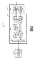
- an exemplary hard disk drive 10 is shown to include a hard disk drive (HDD) system 12 and a hard drive assembly (HDA) 13.
- the HDA 13 includes one or more circular recording surfaces 14.
- the recording surfaces 14 are coated with magnetic layers 15. Data is recorded on the recording surfaces 14 in the form of digital bits called ones and zeros
- a spindle motor shown schematically at 16, rotates the recording surfaces 14.
- the spindle motor 16 rotates the recording surfaces 14 at a fixed speed during read/write operations.
- One or more read/write actuator arms 18 moves relative to the recording surfaces 14 to read and/or write data to/from the recording surfaces 14.
- a read/write device 20 is located near a distal end of the read/write arm 18.
- the read/write device 20 includes a write element such as an inductor that generates a magnetic field,
- the read/write device 20 also includes a read element (such as a magneto-resistive (MR) element) that senses the magnetic field on the recording surfaces 14.
- MR magneto-resistive
- a preamp circuit 22 amplifies analog read/write signals. When reading data, the preamp circuit 22 amplifies low level signals from the read element and outputs the amplified signal to a read channel device 24. When writing data, a write current is generated which flows through the write element of the read/write device 20. The write current is switched to produce a magnetic field having a positive or negative polarity. The positive or negative polarity is stored on the recording surfaces 14 and is used to represent data.
- the HDD 12 typically includes a buffer 32 that stores data that is associated with the control of the hard disk drive. Additionally, the buffer 32 buffers data that is read or that is to be written. The data thus buffered is then transmitted as data blocks to improve efficiency of reading and writing.
- the buffer 32 may employ DRAM, SDRAM, or other types of low latency memory.
- the HDD 12 further includes a processor 34 that performs processing related to the operation of the HDD 10.
- the HDD 12 further includes a hard disk controller (HDC) 36 that communicates with a host device via an input/output (I/O) interface 38.
- the I/O interface 38 can be a serial or parallel interface, such as an Integrated Drive Electronics (IDE), Advanced Technology Attachment (ATA), or serial ATA (SATA) interface.
- IDE Integrated Drive Electronics
- ATA Advanced Technology Attachment
- SATA serial ATA
- the I/O interface 38 communicates with an I/O interface 44 that is associated with a host device 46.
- the HDC 36 also communicates with a spindle/voice coil motor (VCM) driver 40 and/or the read channel device 24.
- the spindle/VCM driver 40 controls the spindle motor 16 that rotates the recording surfaces 14.
- the spindle/VCM driver 40 also generates control signals that position the read/write arm 18 using a voice coil actuator, a stepper motor, or any other suitable actuator.
- the read channel device 24 may incorporate an efficient data-encoding scheme in addition to advanced digital filtering and data-detection techniques.
- the read channel device 24 may thereby increase areal densities and data transfer rates of disk drives.
- testing devices such as the read channel device 24 may ensure data reliability.
- Disk drives are steadily decreasing in size and increasing in speed. This is because use of disk drives is proliferating in small electronic devices such as MP3 players, game consoles, digital cameras, etc. These devices typically use compact disk drives having high storage capacities and high data transfer rates. As a result, physical dimensions of disk drives are steadily shrinking. This makes using external test equipment increasingly impractical. Consequently, conventional test equipment may be unable to test complex devices and subsystems such as read channel devices, hard disk controllers, etc., in compact and high-speed disk drives.
- a system comprises a hard disk controller (HDC) module that controls a hard disk and a read channel (RC) device that communicates with the HDC module via a read bus and a write bus.
- the RC device includes a loopback circuit that selectively loops back the write bus to the read bus.
- the RC device generates a write clock for the HDC module to write data on the write bus and a read clock for the HDC module to read the data on the read bus, wherein the write clock is independent of the read clock.
- the RC device comprises a control module that activates the loopback circuit.
- the RC device generates the write clock based on a fixed RC timebase.
- the RC device generates a read clock based on a recovered channel clock.
- the RC device comprises a write clock generator module that generates the write clock by dividing one of a fixed RC timebase and a recovered channel clock.
- the RC device comprises a clock control module that disables stretching and rephasing features of the write clock generator module.
- the RC device comprises a clock control module that disables switching between the fixed RC timebase and the recovered channel clock after the write clock generator module selects one of the fixed RC timebase and the recovered channel clock to generate the write clock.
- the HDC module is fabricated on a first die and the RC device is fabricated on a second die.
- the HDC module and the RC device are fabricated on a common die.
- a system comprises a hard disk controller (HDC) module that controls a hard disk using a read bus and a write bus, a first-in first-out (FIFO) memory that buffers data on the read bus, and a read channel (RC) device that communicates with the HDC module via the read bus and the write bus.
- the RC device includes a loopback circuit that selectively loops back the write bus to the read bus.
- the RC device generates a loopback clock that clocks the FIFO memory when the write bus is looped back to the read bus.
- the HDC module reads an output of the FIFO memory generated by the loopback clock when the write bus is looped back to the read bus.
- the HDC module reads an output of the FIFO memory generated by a read-write clock when the write bus is not looped back to the read bus.
- the RC device comprises a read-write clock generator that generates a read-write clock for the HDC module to read data on the read bus and to write data on the write bus.
- the read-write clock generator generates the read-write clock based on a fixed RC timebase and a recovered channel clock.
- the read-write clock generator generates the read-write clock based on the fixed RC timebase when the HDC module writes data on the write bus.
- the read-write clock generator generates the read-write clock based on the recovered channel clock when the HDC module reads data from the read bus.
- the HDC module is fabricated on a first die and the RC device is fabricated on a second die.
- the HDC module and the RC device are fabricated on a common die.
- a method comprises selectively looping back a write bus to a read bus between a hard disk controller (HDC) module and a read channel (RC) device in a disk drive, generating a write clock for the HDC module to write data on the write bus, and generating a read clock for the HDC module to read the data on the read bus, wherein the write clock is independent of the read clock.
- HDC hard disk controller
- RC read channel
- the method further comprises generating the write clock based on a fixed RC timebase.
- the method further comprises generating a read clock based on a recovered channel clock.
- the method further comprises generating the write clock by dividing one of a fixed RC timebase and a recovered channel clock.
- the method further comprises disabling stretching and rephasing of the write clock.
- the method further comprises disabling switching between the fixed RC timebase and the recovered channel clock after selecting one of the fixed RC timebase and the recovered channel clock to generate the write clock.
- a method comprises selectively looping back a write bus to a read bus between a hard disk controller (HDC) module and a read channel (RC) device in a disk drive, buffering data on the read bus using a first-in first-out (FIFO) memory, and generating a loopback clock for clocking the FIFO memory when the write bus is looped back to the read bus.
- HDC hard disk controller
- RC read channel
- the method further comprises reading an output of the FIFO memory that is generated by the loopback clock when the write bus is looped back to the read bus.
- the method further comprises reading an output of the FIFO memory that is generated by a read-write clock when the write bus is not looped back to the read bus.
- the method further comprises generating a read-write clock for the HDC module to read data on the read bus and to write data on the write bus.
- the method further comprises generating the read-write clock based on a fixed RC timebase and a recovered channel clock.
- the method further comprises generating the read-write clock based on the fixed RC timebase when the HDC module writes data on the write bus.
- the method further comprises generating the read-write clock based on the recovered channel clock when the HDC module reads data from the read bus.
- a system comprises hard disk controller (HDC) means for controlling a hard disk, and read channel (RC) means for communicating with the HDC means via a read bus and a write bus, selectively looping back the write bus to the read bus using a loopback means, generating a write clock for the HDC means to write data on the write bus, and generating a read clock for the HDC means to read the data on the read bus, wherein the write clock is independent of the read clock.
- HDC hard disk controller
- RC read channel
- the RC means comprises control means for activating the loop back means.
- the RC means generates the write clock based on a fixed RC timebase.
- the RC means generates a read clock based on a recovered channel clock.
- the RC means comprises write clock generator means for generating the write clock by dividing one of a fixed RC timebase and a recovered channel clock.
- the RC means comprises clock control means for disabling stretching and rephasing features of the write clock generator means.
- the RC means comprises clock control means for disabling switching between the fixed RC timebase and the recovered channel clock after the write clock generator means selects one of the fixed RC timebase and the recovered channel clock to generate the write clock.
- the HDC means is fabricated on a first die and the RC means is fabricated on a second die.
- the HDC means and the RC means are fabricated on a common die.
- a system comprises hard disk controller (HDC) means for controlling a hard disk using a read bus and a write bus, first-in first-out (FIFO) memory means for buffering data on the read bus, and read channel (RC) means for communicating with the HDC means via the read bus and the write bus, selectively looping back the write bus to the read bus using loopback means, and generating a loopback clock for clocking the FIFO memory means when the write bus is looped back to the read bus.
- HDC hard disk controller
- FIFO first-in first-out
- RC read channel
- the HDC means reads an output of the FIFO memory means that is generated by the loopback clock when the write bus is looped back to the read bus.
- the HDC means reads an output of the FIFO memory means that is generated by a read-write clock when the write bus is not looped back to the read bus.
- the RC means comprises read-write clock generator means for generating a read-write clock for the HDC means to read data on the read bus and to write data on the write bus.
- the read-write clock generator means generates the read-write clock based on a fixed RC timebase and a recovered channel clock.
- the read-write clock generator means generates the read-write clock based on the fixed RC timebase when the HDC means writes data on the write bus.
- the read-write clock generator means generates the read-write clock based on the recovered channel clock when the HDC means reads data from the read bus.
- the HDC means is fabricated on a first die and the RC means is fabricated on a second die.
- the HDC means and the RC means are fabricated on a common die.
- a computer program executed by a processor comprises selectively looping back a write bus to a read bus between a hard disk controller (HDC) module and a read channel (RC) device in a disk drive, generating a write clock for the HDC module to write data on the write bus, and generating a read clock for the HDC module to read the data on the read bus, wherein the write clock is independent of the read clock.
- HDC hard disk controller
- RC read channel
- the computer program further comprises generating the write clock based on a fixed RC timebase.
- the computer program further comprises generating a read clock based on a recovered channel clock.
- the computer program further comprises generating the write clock by dividing one of a fixed RC timebase and a recovered channel clock.
- the computer program further comprises disabling stretching and rephasing of the write clock.
- the computer program further comprises disabling switching between the fixed RC timebase and the recovered channel clock after selecting one of the fixed RC timebase and the recovered channel clock to generate the write clock.
- a computer program executed by a processor comprises selectively looping back a write bus to a read bus between a hard disk controller (HDC) module and a read channel (RC) device in a disk drive, buffering data on the read bus using a first-in first-out (FIFO) memory, and generating a loopback clock for clocking the FIFO memory when the write bus is looped back to the read bus.
- HDC hard disk controller
- RC read channel
- the computer program further comprises reading an output of the FIFO memory that is generated by the loopback clock when the write bus is looped back to the read bus.
- the computer program further comprises reading an output of the FIFO memory that is generated by a read-write clock when the write bus is not looped back to the read bus.
- the computer program further comprises generating a read-write clock for the HDC module to read data on the read bus and to write data on the write bus.
- the computer program further comprises generating the read-write clock based on a fixed RC timebase and a recovered channel clock.
- the computer program further comprises generating the read-write clock based on the fixed RC timebase when the HDC module writes data on the write bus.
- the computer program further comprises generating the read-write clock based on the recovered channel clock when the HDC module reads data from the read bus.
- the systems and methods described above are implemented by a computer program executed by one or more processors.
- the computer program can reside on a computer readable medium such as but not limited to memory, non-volatile data storage and/or other suitable tangible storage mediums.
- FIG. 1 is a functional block diagram of an exemplary hard disk drive according to the prior art
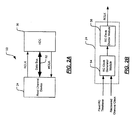
- FIG. 2A is a functional block diagram of an exemplary interface between a read channel device and a hard disk controller module in a hard disk drive;
- FIG. 2B is a functional block diagram of an exemplary clock generator used in a read channel device to generate a read-write clock
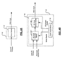
- FIG. 3 is a functional block diagram of an exemplary system for performing loopback tests in a hard disk drive according to the present disclosure
- FIG. 4A is a functional block diagram of an exemplary write clock generator according to the present disclosure.
- FIG. 4B is a functional block diagram of an exemplary write clock generator according to the present disclosure.
- FIG. 5 is a functional block diagram of an exemplary system for performing loopback tests in a hard disk drive according to the present disclsoure;
- FIG. 6 is a flowchart of an exemplary method for performing loopback tests in a hard disk drive according to the present disclosure
- FIG. 7 is a flowchart of an exemplary method for performing loopback tests in a hard disk drive according to the present disclosure
- FIG. 8 is a flowchart of an exemplary method for performing loopback tests in a hard disk drive according to the present disclosure
- FIG. 9A is a functional block diagram of a high definition television
- FIG. 9B is a functional block diagram of a vehicle control system
- FIG. 9C is a functional block diagram of a cellular phone
- FIG. 9D is a functional block diagram of a set top box.
- FIG. 9E is a functional block diagram of a media player.
- module, circuit and/or device refers to an Application Specific Integrated Circuit (ASIC), an electronic circuit, a processor (shared, dedicated, or group) and memory that execute one or more software or firmware programs, a combinational logic circuit, and/or other suitable components that provide the described functionality.
- ASIC Application Specific Integrated Circuit
- processor shared, dedicated, or group
- memory that execute one or more software or firmware programs, a combinational logic circuit, and/or other suitable components that provide the described functionality.
- phrase at least one of A, B, and C should be construed to mean a logical (A or B or C), using a non-exclusive logical or. It should be understood that steps within a method may be executed in different order without altering the principles of the present disclosure.
- loopback circuit typically loops back outputs of an output driver of a device to inputs of an input driver of the device. If data written matches data read back, the device and associated datapaths are considered to be functioning normally. Otherwise, a malfunction is detected.
- Loopbacks can be incorporated in disk drives to perform self-tests. Loopbacks may be used instead of conventional test equipment to test electronic devices and subsystems in disk drives. Loopbacks may be preferable to external test equipment when disk drives are compact in size, high in storage capacity, and have high throughput or data transfer rates.
- an interface 50 between a read channel (RC) device 24 and a hard disk controller (HDC) module 36 of a disk drive comprises a data bus 52, a read/write clock (RCLK), and a return read/write clock (WCLK).
- the data bus 52 comprises read datapaths and write datapaths.
- the HDC module 36 communicates with the RC device 24 via data bus 52. Specifically, the HDC module 36 reads and writes data via data bus 52 using RCLK generated by the RC device 24.
- the RC device 24 comprises a RC clock generator module 54 and a RC clock divider module 56.
- the RC device 24 generates RCLK during normal operation as follows.
- the clock generator module 54 When the HDC module 36 writes data, the clock generator module 54 generates a clock signal based on a fixed RC timebase. This is because write datapaths typically use a clock of a constant periodicity to write data at a constant bit rate.
- the clock generator module 54 when the HDC module 36 reads data, the clock generator module 54 generates the clock signal based on a recovered channel clock.
- the divider module 56 divides the clock signal generated by the RC clock generator module 54 to generate RCLK.
- Switching between fixed RC timebase while writing and recovered channel clock while reading may alter periodicity of RCLK. Additionally, when reading data, the periodicity of RCLK may be altered due to a zero-phase-restart (ZPS) and/or a rephasing of RCLK. ZPS occurs during initial channel synchronization. Rephasing of RCLK may occur when a sync-mark is detected.
- ZPS zero-phase-restart
- Irregularities in the periodicity of RCLK are not problematic in normal read/write operations since normal read/write operations are not performed simultaneously.
- read and write operations are performed simultaneously. That is, read and write datapaths are clocked simultaneously during loopback tests. If RCLK is used to write data during loopback tests, data read back may differ from data written due to irregularities in RCLK rather than due to a fault. Therefore, RCLK cannot be used to write data during loopback tests. Specifically, the clock for write datapaths may not have irregularities even if the clock for read datapaths does.
- the present disclosure discloses various schemes for enabling loopback tests by generating a write clock of a constant periodicity for write datapaths.
- a RC device generates a write clock of a constant periodicity for write datapaths in addition to generating a read clock for read datapaths.
- the write clock does not stretch and/or rephase during ZPS and/or synchronization of the read clock of read datapaths during a read operation.
- a HDC module writes data at a constant rate using the write clock even when the read clock performs timing synchronization, etc.
- a system 60 for performing loopback tests in a disk drive comprises a RC device 25 and a HDC module 37.
- the HDC module 37 writes data on write datapaths (write bus) 52-1 and reads data from datapaths (read bus) 52-2.
- the write datapaths 52-1 are clocked by a write clock generated by the RC device 25.
- the read datapaths 52-2 are clocked by a read clock generated by the RC device.
- the write clock has a constant periodicity even if the read clock may stretch and/or rephase.
- the RC device 25 comprises a loopback control module 61, an input driver module 63, an output driver module 65, a loopback circuit 71, a write clock generator module 62, and a read clock generator module 64.
- the loopback control module 61 activates the loopback circuit 71.
- the loopback circuit 71 effectuates a loopback 70 and loops back the write bus 52-1 to the read bus 52-2.
- the loopback circuit 71 loops back outputs of the output driver module 65 to inputs of the input driver module 63.
- the loopback 70 may be effectuated by an external loopback or a test module (both not shown).
- the write clock generator module 62 generates the write clock using a fixed RC timebase.
- the read clock generator module 64 generates the read clock using a recovered channel clock.
- the HDC module 37 comprises a write module 66 that writes data on the write bus 52-1 using the write clock.
- the HDC module 37 comprises a read module 68 that reads data from the read bus 52-2 using the read clock.
- the write clock generator module 62 may generate the write clock of a constant periodicity in many vvays.
- the write clock generator module 62 comprises a divider module 67 that divides the fixed RC timebase to generate the write clock as shown in FIG. 4A.
- the write clock generator module 62 comprises a RC clock generator module 54-1, a RC clock divider module 56-1, and a clock control module 72 as shown in FIG. 4B.
- the RC clock generator module 54-1 receives the fixed RC timebase and the recovered channel clock as sources for generating the write clock.
- the clock control module 72 disables a source switching feature of the RC clock generator module 54-1.
- the RC clock generator module 54-1 may use the fixed RC timebase or the recovered channel clock as a source for generating the write clock. Once the source is selected, however, the RC clock generator module 54-1 may not switch the source. Additionally, the clock control module 72 disables ZPS clock stretching and rephasing features of the RC clock divider module 56-1.
- the write clock generated by the write clock generator module 62 has a constant periodicity.
- data may be read back during loopback tests using a clock of a constant periodicity.
- a data-flow synchronization circuit such as a first-in first-out (FIFO) memory is used in read datapaths.
- the FIFO memory is clocked with a clock of a constant periodicity during loopback tests.
- the FIFO memory can transfer data from one clock domain such as RCLK that may have irregular periodicity to another clock domain having a constant periodicity.
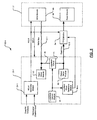
- a system 60-1 for performing loopback tests in a disk drive comprises a RC device 25-1, a HDC module 37, and a first-in first-out (FIFO) memory 74.
- the HDC module 37 writes data on write datapaths (write bus) 52-1 and reads data from read datapaths (read bus) 52-2.
- the RC device 25-1 comprises a RCLK generator module 24-1, a loopback control module 61, a loopback clock generator module 64-1, an input driver module 63, an output driver module 65, and a loopback circuit 71.
- the FIFO memory 74 is a data-flow synchronization circuit that is used in read datapaths 52-2.
- the FIFO memory 74 is normally clocked by RCLK.
- the HDC module 37 reads an output of the FIFO memory 74 that is clocked by RCLK when reading data during normal operation. During loopback tests, however, the FIFO memory 74 is clocked by a loopback clock.
- the HDC module 37 reads an output of the FIFO memory 74 that is clocked by the loopback clock when reading back data during loopback tests.
- the RCLK generator module 24-1 generates RCLK that the HDC module 37 uses to write data on write datapaths 52-1 and to read data on read datapaths 52-2.
- the loopback clock generator module 64-1 generates the loopback clock of a constant periodicity that is used to clock the FIFO memory 74 during loopback tests.
- the loopback control module 61 activates the loopback circuit 71.
- the loopback circuit 71 effectuates a loopback 70 and loops back the write bus 52-1 to the read bus 52-2.
- the loopback circuit 71 loops back outputs of the output driver module 65 to inputs of the input driver module 63.
- the loopback 70 may be effectuated by an external loopback or a test module (not shown).
- the loopback control module 76 activates the loopback clock generator module 64-1.
- the loopback clock generator module 64-1 generates the loopback clock of a constant periodicity that clocks the FIFO memory 74.
- the FIFO memory 74 transfers data from one clock domain such as RCLK that may have irregular periodicity to another clock domain that has a constant periodicity.
- the RC device and the HDC module may be fabricated on separate dies. In some other implementations of systems 60 and 60-1, the RC device and the HDC module may be fabricated on a common die.
- a method 100 for performing self-tests using loopback begins at step 102. If loopback is not enabled in step 104, the method 100 returns to step 102. Otherwise, a RC read clock generator module 64 generates a read clock in step 106 using a recovered channel clock. A write clock generator module 62 generates a write clock in step 108 by dividing a fixed RC timebase. The method 100 ends in step 110.
- a method 150 for performing self-tests using loopback begins at step 152. If loopback is not enabled In step 104, the method 150 returns to step 152. Otherwise, a RC read clock generator module 64 generates a read clock in step 156 using a recovered channel clock.
- a control module 72 disables a clock source switching feature of a RC clock generator module 54-1 in step 158. The control module 72 disables ZPS clock stretching and rephasing features of a RC clock divider module 56-1 in step 160.
- the write clock generator module 62 generates a write clock of a constant periodicity in step 162 using a fixed RC timebase or a recovered channel clock.
- the method 150 ends in step 164.
- a method 200 for performing seff-tests using loopback begins at step 202. If loopback is not enabled in step 204, the method 200 returns to step 202. Otherwise, a RC read clock generator module 64 generates a read clock in step 206 using a recovered channel clock. The write clock generator module 62 generates a write clock of a constant periodicity in step 208.
- a loopback control module 76 uses a clock of a constant periodicity such as the write clock to clock a FIFO memory 72 in read datapaths 52-2 in step 210.
- the FIFO memory 72 transfers data from a clock domain having an irregular clock such as the read clock to a time domain having a constant periodicity in step 212.
- the method 200 ends in step 214.
- the system 60 can be implemented in a mass data storage 427 of a high definition television (HDTV) 420.
- the HDTV 420 receives HDTV input signals in either a wired or wireless format and generates HDTV output signals for a display 426.
- signal processing circuit and/or control circuit 422 and/or other circuits (not shown) of the HDTV 420 may process data, perform coding and/or encryption, perform calculations, format data and/or perform any other type of HDTV processing that may be required.
- the HDTV 420 may communicate with the mass data storage 427 that stores data in a nonvolatile manner such as optical and/or magnetic storage devices.
- the HDD may be a mini HDD that includes one or more platters having a diameter that is smaller than approximately 1.8".
- the HDTV 420 may be connected to memory 428 such as RAM, ROM, low latency nonvolatile memory such as flash memory and/or other suitable electronic data storage.
- the HDTV 420 also may support connections with a WLAN via a WLAN network interface 429.
- a powertrain control system 432 receives inputs from one or more sensors such as temperature sensors, pressure sensors, rotational sensors, airflow sensors and/or any other suitable sensors and/or that generates one or more output control signals such as engine operating parameters, transmission operating parameters, and/or other control signals.
- sensors such as temperature sensors, pressure sensors, rotational sensors, airflow sensors and/or any other suitable sensors and/or that generates one or more output control signals such as engine operating parameters, transmission operating parameters, and/or other control signals.
- a control system 440 may likewise receive signals from input sensors 442 and/or output control signals to one or more output devices 444.
- the control system 440 may be part of an anti-lock braking system (ABS), a navigation system, a telematics system, a vehicle telematics system, a lane departure system, an adaptive cruise control system, a vehicle entertainment system such as a stereo, DVD, compact disc and the like. Still other implementations are contemplated.
- the powertrain control system 432 may communicate with the mass data storage 446 that stores data in a nonvolatile manner.
- the mass data storage 446 may include optical and/or magnetic storage devices such as hard disk drives HDD and/or DVDs.
- the system 60 may be implemented in at least one HDD.
- the HDD may be a mini HDD that includes one or more platters having a diameter that is smaller than approximately 1.8".
- the powertrain control system 432 may be connected to memory 447 such as RAM, ROM, low latency nonvolatile memory such as flash memory and/or other suitable electronic data storage.
- the powertrain control system 432 also may support connections with a WLAN via a WLAN network interface 448.
- the control system 440 may also include mass data storage, memory and/or a WLAN interface (all not shown).
- the system 60 can be implemented in a mass data storage 464 of a cellular phone 450 that may include a cellular antenna 451.
- the cellular phone 450 includes a microphone 456, an audio output 458 such as a speaker and/or audio output jack, a display 460 and/or an input device 462 such as a keypad, pointing device, voice actuation and/or other input device.
- the signal processing and/or control circuits 452 and/or other circuits (not shown) in the cellular phone 450 may process data, perform coding and/or encryption, perform calculations, format data and/or perform other cellular phone functions.
- the cellular phone 450 may communicate with the mass data storage 464 that stores data in a nonvolatile manner such as optical and/or magnetic storage devices for example hard disk drives HDD and/or DVDs.
- the system 60 may be implemented in at least one HDD.
- the HDD may be a mini HDD that includes one or more platters having a diameter that is smaller than approximately 1.8".
- the cellular phone 450 may be connected to memory 466 such as RAM, ROM, low latency nonvolatile memory such as flash memory and/or other suitable electronic data storage.
- the cellular phone 450 also may support connections with a WLAN via a WLAN network interface 468.
- the system 60 can be implemented in a mass data storage 490 of a set top box 480.
- the set top box 480 receives signals from a source such as a broadband source and outputs standard and/or high definition audio/video signals suitable for a display 488 such as a television and/or monitor and/or other video and/or audio output devices.
- the signal processing and/or control circuits 484 and/or other circuits (not shown) of the set top box 480 may process data, perform coding and/or encryption, perform calculations, format data and/or perform any other set top box function.
- the set top box 480 may communicate with the mass data storage 490 that stores data in a nonvolatile manner.
- the mass data storage 490 may include optical and/or magnetic storage devices for example hard disk drives HDD and/or DVDs.
- the system 60 may be implemented in at least one HDD.
- the HDD may be a mini HDD that includes one or more platters having a diameter that is smaller than approximately 1.8".
- the set top box 480 may be connected to memory 494 such as RAM, ROM, low latency nonvolatile memory such as flash memory and/or other suitable electronic data storage.
- the set top box 480 also may support connections with a WLAN via a WLAN network interface 496.
- the system 60 can be implemented in a mass data storage 510 of a media player 500.
- the media player 500 includes a display 507 and/or a user input 508 such as a keypad, touchpad and the like.
- the media player 500 may employ a graphical user interface (GUI) that typically employs menus, drop down menus, icons and/or a point-and-click interface via the display 507 and/or user input 508.
- GUI graphical user interface
- the media player 500 further includes an audio output 509 such as a speaker and/or audio output jack.
- the signal processing and/or control circuits 504 and/or other circuits (not shown) of the media player 500 may process data, perform coding and/or encryption, perform calculations, format data and/or perform any other media player function.
- the media player 500 may communicate with the mass data storage 510 that stores data such as compressed audio and/or video content in a nonvolatile manner.
- the compressed audio files include files that are compliant with MP3 format or other suitable compressed audio and/or video formats.
- the mass data storage 510 may include optical and/or magnetic storage devices for example hard disk drives HDD and/or DVDs.
- the system 60 may be implemented in at least one HDD.
- the HDD may be a mini HDD that includes one or more platters having a diameter that is smaller than approximately 1.8".
- the media player 500 may be connected to memory 514 such as RAM, ROM, low latency nonvolatile memory such as flash memory and/or other suitable electronic data storage.
- the media player 500 also may support connections with a WLAN via a WLAN network interface 516. Still other implementations in addition to those described above are contemplated.
Landscapes
- Signal Processing For Digital Recording And Reproducing (AREA)
- Test And Diagnosis Of Digital Computers (AREA)
Applications Claiming Priority (3)
| Application Number | Priority Date | Filing Date | Title |
|---|---|---|---|
| US75943106P | 2006-01-17 | 2006-01-17 | |
| US80879906P | 2006-05-26 | 2006-05-26 | |
| US11/481,109 US7646555B2 (en) | 2006-01-17 | 2006-07-05 | Testing storage system electronics using loopback |
Publications (1)
| Publication Number | Publication Date |
|---|---|
| EP1808860A1 true EP1808860A1 (en) | 2007-07-18 |
Family
ID=37964115
Family Applications (1)
| Application Number | Title | Priority Date | Filing Date |
|---|---|---|---|
| EP07000463A Ceased EP1808860A1 (en) | 2006-01-17 | 2007-01-10 | Testing storage system electronics using loopback |
Country Status (6)
| Country | Link |
|---|---|
| US (2) | US7646555B2 (enExample) |
| EP (1) | EP1808860A1 (enExample) |
| JP (1) | JP2007226942A (enExample) |
| CN (1) | CN101004919B (enExample) |
| SG (1) | SG134249A1 (enExample) |
| TW (1) | TWI406272B (enExample) |
Families Citing this family (4)
| Publication number | Priority date | Publication date | Assignee | Title |
|---|---|---|---|---|
| US7716540B2 (en) * | 2007-01-03 | 2010-05-11 | Dell Products L.P. | Standalone data storage device electromagnetic interference test setup and procedure |
| TWI402671B (zh) * | 2008-09-05 | 2013-07-21 | Hon Hai Prec Ind Co Ltd | 一種sata介面測試系統及方法 |
| US8607104B2 (en) * | 2010-12-20 | 2013-12-10 | Advanced Micro Devices, Inc. | Memory diagnostics system and method with hardware-based read/write patterns |
| US20240205172A1 (en) * | 2022-12-20 | 2024-06-20 | Dell Products L.P. | Packet forwarding in an information handling system with loopback configuration |
Citations (1)
| Publication number | Priority date | Publication date | Assignee | Title |
|---|---|---|---|---|
| US6397042B1 (en) * | 1998-03-06 | 2002-05-28 | Texas Instruments Incorporated | Self test of an electronic device |
Family Cites Families (11)
| Publication number | Priority date | Publication date | Assignee | Title |
|---|---|---|---|---|
| US5729511A (en) * | 1991-02-15 | 1998-03-17 | Discovision Associates | Optical disc system having servo motor and servo error detection assembly operated relative to monitored quad sum signal |
| US5479098A (en) * | 1993-03-15 | 1995-12-26 | Trace Mountain Products, Inc. | Loop-back circuit for testing a magnetic recording system with simultaneous read and write functions |
| JP2882245B2 (ja) * | 1993-07-29 | 1999-04-12 | 日本電気株式会社 | 磁気ディスク制御装置の自己診断方式 |
| TW299439B (enExample) * | 1995-04-11 | 1997-03-01 | Discovision Ass | |
| JP3790329B2 (ja) * | 1997-06-27 | 2006-06-28 | 富士通株式会社 | 信号ループバック装置 |
| US7099278B2 (en) * | 2001-08-10 | 2006-08-29 | Broadcom Corporation | Line loop back for very high speed application |
| JP2004030797A (ja) * | 2002-06-26 | 2004-01-29 | Nec Micro Systems Ltd | リードチャネル半導体集積回路 |
| JP2004030827A (ja) * | 2002-06-27 | 2004-01-29 | Fujitsu Ltd | 記録データ読み取り装置及び記録データ読み取り方法 |
| JP2005158107A (ja) * | 2003-11-21 | 2005-06-16 | Ricoh Co Ltd | 光ディスク記録再生装置の信号処理回路 |
| US7477467B1 (en) * | 2003-11-25 | 2009-01-13 | Marvell International Ltd. | Preamp circuit including a loopback mode for data storage |
| US7250751B2 (en) * | 2005-07-26 | 2007-07-31 | Marvell International Ltd. | Integrated systems testing |
-
2006
- 2006-07-05 US US11/481,109 patent/US7646555B2/en active Active
-
2007
- 2007-01-10 EP EP07000463A patent/EP1808860A1/en not_active Ceased
- 2007-01-16 SG SG200700225-6A patent/SG134249A1/en unknown
- 2007-01-16 CN CN2007100002558A patent/CN101004919B/zh not_active Expired - Fee Related
- 2007-01-17 JP JP2007008412A patent/JP2007226942A/ja active Pending
- 2007-01-17 TW TW096101812A patent/TWI406272B/zh not_active IP Right Cessation
-
2010
- 2010-01-11 US US12/685,249 patent/US8031424B2/en active Active
Patent Citations (1)
| Publication number | Priority date | Publication date | Assignee | Title |
|---|---|---|---|---|
| US6397042B1 (en) * | 1998-03-06 | 2002-05-28 | Texas Instruments Incorporated | Self test of an electronic device |
Non-Patent Citations (1)
| Title |
|---|
| MATTHES D ET AL: "TECHNIQUE FOR TESTING A VERY HIGH SPEED MIXED SIGNAL READ CHANNEL DESIGN", PROCEEDINGS INTERNATIONAL TEST CONFERENCE 2000. ITC 2000. BALTIMORE, MD, OCT. 30 - NOV. 1, 2000, INTERNATIONAL TEST CONFERENCE, NEW YORK, NY : IEEE, US, 30 October 2000 (2000-10-30), pages 965 - 970, XP001049696, ISBN: 0-7803-6547-X * |
Also Published As
| Publication number | Publication date |
|---|---|
| US20100110574A1 (en) | 2010-05-06 |
| US20070165318A1 (en) | 2007-07-19 |
| TW200746085A (en) | 2007-12-16 |
| CN101004919A (zh) | 2007-07-25 |
| US7646555B2 (en) | 2010-01-12 |
| US8031424B2 (en) | 2011-10-04 |
| SG134249A1 (en) | 2007-08-29 |
| JP2007226942A (ja) | 2007-09-06 |
| TWI406272B (zh) | 2013-08-21 |
| CN101004919B (zh) | 2011-07-06 |
Similar Documents
| Publication | Publication Date | Title |
|---|---|---|
| US8935591B1 (en) | System and method to correct errors in data read from a source supplying streaming data | |
| KR101502107B1 (ko) | Usb 애플리케이션에서의 모바일 드라이브를 위한 최저 파워 모드 | |
| US8019957B1 (en) | Method and system for automatic calibration of a DQS signal in a storage controller | |
| US7788427B1 (en) | Flash memory interface for disk drive | |
| EP1610212A2 (en) | Bridge circuit | |
| US7561361B1 (en) | Dynamic synchronization of timing signals | |
| US7733588B1 (en) | Repetitive feed-forward algorithm for self-servo-write PLL | |
| CN101681298A (zh) | 存储器控制器 | |
| US8046185B1 (en) | Oscillator calibration for motor controller | |
| US20090091855A1 (en) | Method for improved insitu spiral writing | |
| US8031424B2 (en) | Method and apparatus for testing electronics of a storage system | |
| US7945812B1 (en) | System and method for error correction | |
| JP2007184023A (ja) | ディスク・ドライブ及びその制御方法 | |
| US7827387B1 (en) | Communication bus with hidden pre-fetch registers | |
| US7937526B1 (en) | Storage device cache with phase change memory | |
| US9001443B1 (en) | Method and system for testing a controller of a hard disk drive | |
| US8078687B1 (en) | System and method for data management | |
| US20140173346A1 (en) | Validating operation of system-on-chip controller for storage device using programmable state machine | |
| HK1109489A (en) | Testing storage system electronics using loopback | |
| CN100550164C (zh) | 数据存储装置以及控制其用户数据写入的方法 | |
| US8922931B1 (en) | Disk drive releasing variable amount of buffered write data based on sliding window of predicted servo quality | |
| JP4868951B2 (ja) | 制御装置、記憶装置およびヘッド退避方法 | |
| JP2007317263A (ja) | シリアル・データ転送方法、そのシステム及びデータ記憶装置 |
Legal Events
| Date | Code | Title | Description |
|---|---|---|---|
| PUAI | Public reference made under article 153(3) epc to a published international application that has entered the european phase |
Free format text: ORIGINAL CODE: 0009012 |
|
| AK | Designated contracting states |
Kind code of ref document: A1 Designated state(s): AT BE BG CH CY CZ DE DK EE ES FI FR GB GR HU IE IS IT LI LT LU LV MC NL PL PT RO SE SI SK TR |
|
| AX | Request for extension of the european patent |
Extension state: AL BA HR MK YU |
|
| 17P | Request for examination filed |
Effective date: 20080116 |
|
| 17Q | First examination report despatched |
Effective date: 20080227 |
|
| AKX | Designation fees paid |
Designated state(s): DE FR GB |
|
| STAA | Information on the status of an ep patent application or granted ep patent |
Free format text: STATUS: THE APPLICATION HAS BEEN REFUSED |
|
| 18R | Application refused |
Effective date: 20170903 |