EP1804562A1 - Composite multilayer substrate and its manufacturing method - Google Patents
Composite multilayer substrate and its manufacturing method Download PDFInfo
- Publication number
- EP1804562A1 EP1804562A1 EP05793224A EP05793224A EP1804562A1 EP 1804562 A1 EP1804562 A1 EP 1804562A1 EP 05793224 A EP05793224 A EP 05793224A EP 05793224 A EP05793224 A EP 05793224A EP 1804562 A1 EP1804562 A1 EP 1804562A1
- Authority
- EP
- European Patent Office
- Prior art keywords
- multilayer substrate
- ceramic
- resin portion
- cavity
- substrate
- Prior art date
- Legal status (The legal status is an assumption and is not a legal conclusion. Google has not performed a legal analysis and makes no representation as to the accuracy of the status listed.)
- Granted
Links
Images

Classifications
-
- H—ELECTRICITY
- H05—ELECTRIC TECHNIQUES NOT OTHERWISE PROVIDED FOR
- H05K—PRINTED CIRCUITS; CASINGS OR CONSTRUCTIONAL DETAILS OF ELECTRIC APPARATUS; MANUFACTURE OF ASSEMBLAGES OF ELECTRICAL COMPONENTS
- H05K1/00—Printed circuits
- H05K1/18—Printed circuits structurally associated with non-printed electric components
- H05K1/182—Printed circuits structurally associated with non-printed electric components associated with components mounted in printed circuit boards [PCB], e.g. insert-mounted components [IMC]
- H05K1/183—Printed circuits structurally associated with non-printed electric components associated with components mounted in printed circuit boards [PCB], e.g. insert-mounted components [IMC] associated with components mounted in and supported by recessed areas of the PCBs
-
- H—ELECTRICITY
- H05—ELECTRIC TECHNIQUES NOT OTHERWISE PROVIDED FOR
- H05K—PRINTED CIRCUITS; CASINGS OR CONSTRUCTIONAL DETAILS OF ELECTRIC APPARATUS; MANUFACTURE OF ASSEMBLAGES OF ELECTRICAL COMPONENTS
- H05K1/00—Printed circuits
- H05K1/18—Printed circuits structurally associated with non-printed electric components
- H05K1/182—Printed circuits structurally associated with non-printed electric components associated with components mounted in printed circuit boards [PCB], e.g. insert-mounted components [IMC]
- H05K1/185—Printed circuits structurally associated with non-printed electric components associated with components mounted in printed circuit boards [PCB], e.g. insert-mounted components [IMC] associated with components encapsulated in the insulating substrate of the PCBs; associated with components incorporated in internal layers of multilayer circuit boards
- H05K1/186—Printed circuits structurally associated with non-printed electric components associated with components mounted in printed circuit boards [PCB], e.g. insert-mounted components [IMC] associated with components encapsulated in the insulating substrate of the PCBs; associated with components incorporated in internal layers of multilayer circuit boards manufactured by mounting on or connecting to patterned circuits before or during embedding
-
- H—ELECTRICITY
- H05—ELECTRIC TECHNIQUES NOT OTHERWISE PROVIDED FOR
- H05K—PRINTED CIRCUITS; CASINGS OR CONSTRUCTIONAL DETAILS OF ELECTRIC APPARATUS; MANUFACTURE OF ASSEMBLAGES OF ELECTRICAL COMPONENTS
- H05K3/00—Apparatus or processes for manufacturing printed circuits
- H05K3/46—Manufacturing multilayer circuits
- H05K3/4697—Manufacturing multilayer circuits having cavities, e.g. for mounting components
-
- H—ELECTRICITY
- H10—SEMICONDUCTOR DEVICES; ELECTRIC SOLID-STATE DEVICES NOT OTHERWISE PROVIDED FOR
- H10W—GENERIC PACKAGES, INTERCONNECTIONS, CONNECTORS OR OTHER CONSTRUCTIONAL DETAILS OF DEVICES COVERED BY CLASS H10
- H10W70/00—Package substrates; Interposers; Redistribution layers [RDL]
- H10W70/60—Insulating or insulated package substrates; Interposers; Redistribution layers
- H10W70/611—Insulating or insulated package substrates; Interposers; Redistribution layers for connecting multiple chips together
- H10W70/614—Insulating or insulated package substrates; Interposers; Redistribution layers for connecting multiple chips together the multiple chips being integrally enclosed
-
- H—ELECTRICITY
- H10—SEMICONDUCTOR DEVICES; ELECTRIC SOLID-STATE DEVICES NOT OTHERWISE PROVIDED FOR
- H10W—GENERIC PACKAGES, INTERCONNECTIONS, CONNECTORS OR OTHER CONSTRUCTIONAL DETAILS OF DEVICES COVERED BY CLASS H10
- H10W90/00—Package configurations
-
- H—ELECTRICITY
- H05—ELECTRIC TECHNIQUES NOT OTHERWISE PROVIDED FOR
- H05K—PRINTED CIRCUITS; CASINGS OR CONSTRUCTIONAL DETAILS OF ELECTRIC APPARATUS; MANUFACTURE OF ASSEMBLAGES OF ELECTRICAL COMPONENTS
- H05K1/00—Printed circuits
- H05K1/02—Details
- H05K1/03—Use of materials for the substrate
- H05K1/0306—Inorganic insulating substrates, e.g. ceramic, glass
-
- H—ELECTRICITY
- H05—ELECTRIC TECHNIQUES NOT OTHERWISE PROVIDED FOR
- H05K—PRINTED CIRCUITS; CASINGS OR CONSTRUCTIONAL DETAILS OF ELECTRIC APPARATUS; MANUFACTURE OF ASSEMBLAGES OF ELECTRICAL COMPONENTS
- H05K1/00—Printed circuits
- H05K1/02—Details
- H05K1/03—Use of materials for the substrate
- H05K1/0313—Organic insulating material
-
- H—ELECTRICITY
- H05—ELECTRIC TECHNIQUES NOT OTHERWISE PROVIDED FOR
- H05K—PRINTED CIRCUITS; CASINGS OR CONSTRUCTIONAL DETAILS OF ELECTRIC APPARATUS; MANUFACTURE OF ASSEMBLAGES OF ELECTRICAL COMPONENTS
- H05K2203/00—Indexing scheme relating to apparatus or processes for manufacturing printed circuits covered by H05K3/00
- H05K2203/06—Lamination
- H05K2203/061—Lamination of previously made multilayered subassemblies
-
- H—ELECTRICITY
- H05—ELECTRIC TECHNIQUES NOT OTHERWISE PROVIDED FOR
- H05K—PRINTED CIRCUITS; CASINGS OR CONSTRUCTIONAL DETAILS OF ELECTRIC APPARATUS; MANUFACTURE OF ASSEMBLAGES OF ELECTRICAL COMPONENTS
- H05K2203/00—Indexing scheme relating to apparatus or processes for manufacturing printed circuits covered by H05K3/00
- H05K2203/06—Lamination
- H05K2203/063—Lamination of preperforated insulating layer
-
- H—ELECTRICITY
- H05—ELECTRIC TECHNIQUES NOT OTHERWISE PROVIDED FOR
- H05K—PRINTED CIRCUITS; CASINGS OR CONSTRUCTIONAL DETAILS OF ELECTRIC APPARATUS; MANUFACTURE OF ASSEMBLAGES OF ELECTRICAL COMPONENTS
- H05K2203/00—Indexing scheme relating to apparatus or processes for manufacturing printed circuits covered by H05K3/00
- H05K2203/16—Inspection; Monitoring; Aligning
- H05K2203/167—Using mechanical means for positioning, alignment or registration, e.g. using rod-in-hole alignment
-
- H—ELECTRICITY
- H05—ELECTRIC TECHNIQUES NOT OTHERWISE PROVIDED FOR
- H05K—PRINTED CIRCUITS; CASINGS OR CONSTRUCTIONAL DETAILS OF ELECTRIC APPARATUS; MANUFACTURE OF ASSEMBLAGES OF ELECTRICAL COMPONENTS
- H05K3/00—Apparatus or processes for manufacturing printed circuits
- H05K3/22—Secondary treatment of printed circuits
- H05K3/28—Applying non-metallic protective coatings
- H05K3/284—Applying non-metallic protective coatings for encapsulating mounted components
-
- H—ELECTRICITY
- H05—ELECTRIC TECHNIQUES NOT OTHERWISE PROVIDED FOR
- H05K—PRINTED CIRCUITS; CASINGS OR CONSTRUCTIONAL DETAILS OF ELECTRIC APPARATUS; MANUFACTURE OF ASSEMBLAGES OF ELECTRICAL COMPONENTS
- H05K3/00—Apparatus or processes for manufacturing printed circuits
- H05K3/46—Manufacturing multilayer circuits
- H05K3/4611—Manufacturing multilayer circuits by laminating two or more circuit boards
- H05K3/4614—Manufacturing multilayer circuits by laminating two or more circuit boards the electrical connections between the circuit boards being made during lamination
-
- H—ELECTRICITY
- H05—ELECTRIC TECHNIQUES NOT OTHERWISE PROVIDED FOR
- H05K—PRINTED CIRCUITS; CASINGS OR CONSTRUCTIONAL DETAILS OF ELECTRIC APPARATUS; MANUFACTURE OF ASSEMBLAGES OF ELECTRICAL COMPONENTS
- H05K3/00—Apparatus or processes for manufacturing printed circuits
- H05K3/46—Manufacturing multilayer circuits
- H05K3/4688—Composite multilayer circuits, i.e. comprising insulating layers having different properties
-
- H—ELECTRICITY
- H10—SEMICONDUCTOR DEVICES; ELECTRIC SOLID-STATE DEVICES NOT OTHERWISE PROVIDED FOR
- H10W—GENERIC PACKAGES, INTERCONNECTIONS, CONNECTORS OR OTHER CONSTRUCTIONAL DETAILS OF DEVICES COVERED BY CLASS H10
- H10W70/00—Package substrates; Interposers; Redistribution layers [RDL]
- H10W70/60—Insulating or insulated package substrates; Interposers; Redistribution layers
- H10W70/67—Insulating or insulated package substrates; Interposers; Redistribution layers characterised by their insulating layers or insulating parts
- H10W70/68—Shapes or dispositions thereof
- H10W70/682—Shapes or dispositions thereof comprising holes having chips therein
-
- H—ELECTRICITY
- H10—SEMICONDUCTOR DEVICES; ELECTRIC SOLID-STATE DEVICES NOT OTHERWISE PROVIDED FOR
- H10W—GENERIC PACKAGES, INTERCONNECTIONS, CONNECTORS OR OTHER CONSTRUCTIONAL DETAILS OF DEVICES COVERED BY CLASS H10
- H10W70/00—Package substrates; Interposers; Redistribution layers [RDL]
- H10W70/60—Insulating or insulated package substrates; Interposers; Redistribution layers
- H10W70/67—Insulating or insulated package substrates; Interposers; Redistribution layers characterised by their insulating layers or insulating parts
- H10W70/68—Shapes or dispositions thereof
- H10W70/685—Shapes or dispositions thereof comprising multiple insulating layers
-
- H—ELECTRICITY
- H10—SEMICONDUCTOR DEVICES; ELECTRIC SOLID-STATE DEVICES NOT OTHERWISE PROVIDED FOR
- H10W—GENERIC PACKAGES, INTERCONNECTIONS, CONNECTORS OR OTHER CONSTRUCTIONAL DETAILS OF DEVICES COVERED BY CLASS H10
- H10W72/00—Interconnections or connectors in packages
- H10W72/071—Connecting or disconnecting
- H10W72/0711—Apparatus therefor
- H10W72/07141—Means for applying energy, e.g. ovens or lasers
-
- H—ELECTRICITY
- H10—SEMICONDUCTOR DEVICES; ELECTRIC SOLID-STATE DEVICES NOT OTHERWISE PROVIDED FOR
- H10W—GENERIC PACKAGES, INTERCONNECTIONS, CONNECTORS OR OTHER CONSTRUCTIONAL DETAILS OF DEVICES COVERED BY CLASS H10
- H10W74/00—Encapsulations, e.g. protective coatings
-
- H—ELECTRICITY
- H10—SEMICONDUCTOR DEVICES; ELECTRIC SOLID-STATE DEVICES NOT OTHERWISE PROVIDED FOR
- H10W—GENERIC PACKAGES, INTERCONNECTIONS, CONNECTORS OR OTHER CONSTRUCTIONAL DETAILS OF DEVICES COVERED BY CLASS H10
- H10W90/00—Package configurations
- H10W90/701—Package configurations characterised by the relative positions of pads or connectors relative to package parts
- H10W90/721—Package configurations characterised by the relative positions of pads or connectors relative to package parts of bump connectors
- H10W90/724—Package configurations characterised by the relative positions of pads or connectors relative to package parts of bump connectors between a chip and a stacked insulating package substrate, interposer or RDL
-
- H—ELECTRICITY
- H10—SEMICONDUCTOR DEVICES; ELECTRIC SOLID-STATE DEVICES NOT OTHERWISE PROVIDED FOR
- H10W—GENERIC PACKAGES, INTERCONNECTIONS, CONNECTORS OR OTHER CONSTRUCTIONAL DETAILS OF DEVICES COVERED BY CLASS H10
- H10W90/00—Package configurations
- H10W90/701—Package configurations characterised by the relative positions of pads or connectors relative to package parts
- H10W90/751—Package configurations characterised by the relative positions of pads or connectors relative to package parts of bond wires
- H10W90/754—Package configurations characterised by the relative positions of pads or connectors relative to package parts of bond wires between a chip and a stacked insulating package substrate, interposer or RDL
-
- Y—GENERAL TAGGING OF NEW TECHNOLOGICAL DEVELOPMENTS; GENERAL TAGGING OF CROSS-SECTIONAL TECHNOLOGIES SPANNING OVER SEVERAL SECTIONS OF THE IPC; TECHNICAL SUBJECTS COVERED BY FORMER USPC CROSS-REFERENCE ART COLLECTIONS [XRACs] AND DIGESTS
- Y10—TECHNICAL SUBJECTS COVERED BY FORMER USPC
- Y10T—TECHNICAL SUBJECTS COVERED BY FORMER US CLASSIFICATION
- Y10T428/00—Stock material or miscellaneous articles
- Y10T428/24—Structurally defined web or sheet [e.g., overall dimension, etc.]
- Y10T428/24273—Structurally defined web or sheet [e.g., overall dimension, etc.] including aperture
- Y10T428/24322—Composite web or sheet
-
- Y—GENERAL TAGGING OF NEW TECHNOLOGICAL DEVELOPMENTS; GENERAL TAGGING OF CROSS-SECTIONAL TECHNOLOGIES SPANNING OVER SEVERAL SECTIONS OF THE IPC; TECHNICAL SUBJECTS COVERED BY FORMER USPC CROSS-REFERENCE ART COLLECTIONS [XRACs] AND DIGESTS
- Y10—TECHNICAL SUBJECTS COVERED BY FORMER USPC
- Y10T—TECHNICAL SUBJECTS COVERED BY FORMER US CLASSIFICATION
- Y10T428/00—Stock material or miscellaneous articles
- Y10T428/24—Structurally defined web or sheet [e.g., overall dimension, etc.]
- Y10T428/24273—Structurally defined web or sheet [e.g., overall dimension, etc.] including aperture
- Y10T428/24322—Composite web or sheet
- Y10T428/24331—Composite web or sheet including nonapertured component
-
- Y—GENERAL TAGGING OF NEW TECHNOLOGICAL DEVELOPMENTS; GENERAL TAGGING OF CROSS-SECTIONAL TECHNOLOGIES SPANNING OVER SEVERAL SECTIONS OF THE IPC; TECHNICAL SUBJECTS COVERED BY FORMER USPC CROSS-REFERENCE ART COLLECTIONS [XRACs] AND DIGESTS
- Y10—TECHNICAL SUBJECTS COVERED BY FORMER USPC
- Y10T—TECHNICAL SUBJECTS COVERED BY FORMER US CLASSIFICATION
- Y10T428/00—Stock material or miscellaneous articles
- Y10T428/24—Structurally defined web or sheet [e.g., overall dimension, etc.]
- Y10T428/24802—Discontinuous or differential coating, impregnation or bond [e.g., artwork, printing, retouched photograph, etc.]
- Y10T428/24917—Discontinuous or differential coating, impregnation or bond [e.g., artwork, printing, retouched photograph, etc.] including metal layer
Definitions
- the present invention relates to hybrid multilayer substrates and methods for manufacturing the same, and more particularly, relates to a highly reliable hybrid multilayer substrate having a cavity in which an electronic component is mounted with high accuracy, and to a method for manufacturing the hybrid multilayer substrate.
- a wiring substrate having a cavity disclosed in Patent Document 1 may be mentioned.
- This wiring substrate is formed of a ceramic core substrate having a penetrating hole, a resin insulating layer which is formed on the bottom surface of this ceramic core substrate and which blocks up the penetrating hole to form a cavity, an IC chip mounted in the cavity formed by the resin insulating layer, and a filling material which is filled around the IC chip to seal it in the cavity.
- the IC chip is aligned in the penetrating hole of the ceramic core substrate, and the filling material is then filled in a gap between the IC chip and the penetrating hole so as to unite the IC chip and the ceramic core substrate in the penetrating hole.
- a resin insulating layer having via holes is formed on the rear surface of the ceramic core substrate.
- Patent Document 1 Japanese Unexamined Patent Application Publication No. 2003-309213
- the electrodes 2A In order to use the self-alignment function of the IC chip, it is necessary to form a cavity 3 beforehand by thermocompression bonding of a resin insulating layer 2 having electrodes 2A to a ceramic substrate 1 having a penetrating hole as shown in Fig. 11. Furthermore, concomitant with the increase in the number of pins because of the narrower pitch and smaller bumps of an IC chip, the electrodes 2A must be formed with high accuracy in the cavity 3 so as to reduce the shift in position of the electrodes 2A as small as possible.
- the present invention has been conceived in order to solve the problems described above, and an obj ect of the present invention is to provide a hybrid multilayer substrate and a method for manufacturing the same, the hybrid multilayer substrate having high arrangement accuracy of terminal electrodes and the like provided in the bottom surface of the cavity and being capable of significantly improving the reliability in connection with a mounted component.
- a method for manufacturing a hybrid multilayer substrate having a cavity in a laminate structure made of a resin portion and a ceramic substrate which comprises the steps of: forming a resin portion having a protrusion part and a ceramic substrate having a penetrating hole; and bonding the resin portion to the ceramic substrate so as to fit the protrusion part of the resin portion to an end part of the penetrating hole of the ceramic substrate the resin portion. Accordingly, the ceramic substrate and the resin portion are united to form a cavity using an upper surface of the protrusion part as a bottom surface.
- the method for manufacturing a hybrid multilayer substrate which is described in Claim 2 of the present invention, is in accordance with Claim 1 of the present invention, in which the resin portion and the ceramic substrate are compression-bonded to each other.
- the method for manufacturing a hybrid multilayer substrate which is described in Claim 3 of the present invention, is in accordance with Claim 1 or 2 of the present invention, and further comprises the step of placing a first chip type electronic component in the cavity.
- the method for manufacturing a hybrid multilayer substrate which is described in Claim 4 of the present invention, is in accordance with Claim 3 of the present invention, and further comprises the step of sealing the first chip type electronic component placed in the cavity with a resin.
- the method for manufacturing a hybrid multilayer substrate which is described in Claim 5 of the present invention, is in accordance with one of Claims 1 to 4 of the present invention, in which the ceramic substrate is formed as a ceramic multilayer substrate composed of ceramic layers laminated to each other, and in which a predetermined conductive pattern is formed inside the ceramic multilayer substrate and on a surface thereof.
- the method for manufacturing a hybrid multilayer substrate which is described in Claim 6 of the present invention, is in accordance with Claim 5 of the present invention, in which the ceramic layers are formed using a low temperature sintered ceramic, and for the conductive pattern, a conductive material primarily composed of silver or copper is used.
- the method for manufacturing a hybrid multilayer substrate which is described in Claim 7 of the present invention, is in accordance with Claim 5 or 6 of the present invention, in which a terminal electrode is formed in the surface of the resin portion opposite to the surface bonded to the ceramic multilayer substrate, and this terminal electrode is connected to the conductive pattern formed for the ceramic multilayer substrate via a via conductor formed in the resin portion.
- the method for manufacturing a hybrid multilayer substrate which is described in Claim 8 of the present invention, is in accordance with one of Claims 1 to 7 of the present invention, wherein a region, in which a conductive pattern is not formed at the interface between the resin portion and the ceramic substrate and on the bottom surface of the cavity, is formed to be extended from an inside wall surface of the cavity, which is used as the center, to a position 150 ⁇ m or more apart therefrom in every direction.
- the method for manufacturing a hybrid multilayer substrate which is described in Claim 9 of the present invention, is in accordance with one of Claims 3 to 8 of the present invention, and further comprises the step of placing a second chip type electronic component in the resin portion.
- a hybrid multilayer substrate having a cavity in a laminate structure made of a resin portion and a ceramic substrate, in which the resin portion has a protrusion part and the ceramic substrate has a penetrating hole, and the cavity is formed of an upper surface of the protrusion part of the resin portion and a wall surface of the penetrating hole of the ceramic substrate.
- hybrid multilayer substrate described in Claim 11 of the present invention is in accordance with Claim 10 of the present invention, in which a first chip type electronic component is placed in the cavity.
- hybrid multilayer substrate described in Claim 12 of the present invention is in accordance with Claim 11 of the present invention, in which the first chip type electronic component placed in the cavity is sealed with a resin.
- the hybrid multilayer substrate described in Claim 13 of the present invention is in accordance with one of Claims 10 to 12 of the present invention, in which the ceramic substrate is a ceramic multilayer substrate composed of ceramic layers laminated to each other, and a predetermined conductive pattern is formed inside the ceramic multilayer substrate and on a surface thereof.
- the hybrid multilayer substrate described in Claim 14 of the present invention is in accordance with Claim 13 of the present invention, in which the ceramic layers are each formed using a low temperature sintered ceramic layer, and the conductive pattern is formed of a conductive material primarily composed of silver or copper.
- the hybrid multilayer substrate described in Claim 15 of the present invention is in accordance with Claim 13 or 14 of the present invention, in which a terminal electrode is formed in the surface of the resin portion opposite to the surface bonded to the ceramic multilayer substrate, and the terminal electrode is connected to the conductive pattern formed for the ceramic multilayer substrate via a via conductor formed in the resin portion.
- the hybrid multilayer substrate described in Claim 16 of the present invention is in accordance with one of Claims 13 to 15 of the present invention, wherein a region, in which a conductive pattern is not formed at the interface between the resin portion and the ceramic substrate and on the bottom surface of the cavity, is formed from an inside wall surface of the cavity, which is used as the center, to a position 150 ⁇ m or more apart therefrom in every direction.
- a hybrid multilayer substrate and a method for manufacturing the same can be provided, the hybrid multilayer substrate having high arrangement accuracy of terminal electrodes and the like provided in the bottom surface of the cavity and being capable of significantly improving the reliability in connection with a mounted component.
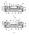
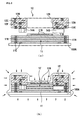
- a hybrid multilayer substrate 10 of this embodiment has, as shown in Fig. 1(a) by way of example, a cavity 10A in a laminate structure which is formed of a resin portion 11 and a ceramic substrate 12 laminated thereon, and is mounted on a mounting substrate (not shown) , such as a printed circuit board, with the resin portion 11 provided therebetween.
- a mounting substrate such as a printed circuit board
- mounting may be performed with the ceramic substrate 12 provided therebetween.
- the resin portion 11 is preferably formed of a resin having a thermal expansion coefficient between the thermal expansion coefficient of the ceramic substrate 12 and that of the mounting substrate, such as an intermediate thermal expansion coefficient therebetween, or a resin having a thermal expansion coefficient gradient therebetween.
- the resin portion 11 is present between the ceramic substrate 12 and the mounting substrate to reduce the difference in thermal expansion between the hybrid multilayer substrate 10 and the mounting substrate, and as a result, the hybrid multilayer substrate 10 mounted on the mounting substrate is not easily removed therefrom even in a high temperature atmosphere.
- This resin portion 11 is formed to have a laminate structure composed of resin layers 11A laminated to each other as shown in the figure, and the ceramic substrate 12 is formed as a ceramic multilayer substrate including ceramic layers 12A laminated to each other. Hence, hereinafter, the ceramic substrate 12 will be described as a ceramic multilayer substrate 12.
- a protrusion part 11B having a flat front surface is formed at a central part of the upper surface of the resin portion 11, and a penetrating hole 12B corresponding to the protrusion part 11B of the resin portion 11 is formed in the ceramic multilayer substrate 12.
- the protrusion part 11B of the resin portion 11 is fitted to a bottom end part of the penetrating hole 12B of the ceramic multilayer substrate 12, the resin portion 11 and the ceramic multilayer substrate 12 are united, so that the cavity 10A of the hybrid multilayer substrate 10 is formed.
- the height of the protrusion part 11B may be at least 10 ⁇ m and is more preferably 50 ⁇ m or more.
- the height of the protrusion part 11B is more than 500 ⁇ m, since a protrusion region under the bottom surface of the cavity 10A is a useless region, the height of the protrusion part 11B is preferably set to 500 ⁇ m or less. Since the protrusion part 11B of the resin portion 11 is fitted to the bottom end part of the penetrating hole 12B of the ceramic multilayer substrate 12, a bonding strength between the resin portion 11 and the ceramic multilayer substrate 12 can be improved, and as a result, the reliability as the hybrid multilayer substrate 10 can be enhanced.
- a first chip type electronic component 13 is provided in the cavity 10A.
- second chip type electronic components 14A and 14B mounted on the bottom surface of the ceramic substrate 12 are embedded in the resin portion 11, the resin portion 11 can be further effectively used as a mounting space for the second chip type electronic components 14A and 14B, and hence functions of the hybrid multilayer substrate 10 can be increased so as to satisfy the trend toward enhancement of multifunctionality.
- a resin is filled in the cavity 10A, and by this resin, the first chip type electronic component 13 is sealed.
- This resin portion (hereinafter referred to as a "sealing resin portion") 15 has an upper surface flush with the upper surface of the ceramic multilayer substrate 12, so that one flat surface is formed.
- the first and the second chip type electronic components 13, 14A, and 14B are respectively sealed with the resins, the first and the second chip type electronic components 13, 14A, and 14B are protected from external mechanical shock, moisture, and the like.
- external terminal electrodes 11C are formed in the bottom surface of the resin portion 11 to have a predetermined pattern, and electrical connection to the mounting substrate is performed via the external terminal electrodes 11C.
- External terminal electrodes 11D having a predetermined pattern are formed in the upper surface of the protrusion part 11B of the resin portion 11 and are connected to the first chip type electronic component 13 placed in the cavity 10A.
- via conductors 11E are provided in the resin portion 11 and serve to connect between a conductive pattern of the ceramic multilayer substrate 12 and a conductive pattern of the mounting substrate.
- External terminal electrodes present at the bonding surface between the resin portion 11 and the ceramic multilayer substrate 12 are not formed at the resin portion 11 side by the reason to be described below and are formed at the ceramic multilayer substrate 12 side.
- the resin layer 11A is preferably formed from a mixed resin composition containing a thermosetting resin and an inorganic filler.
- a thermosetting resin for example, an epoxy resin, a phenol resin, or a cyanate resin, which has superior heat resistance and humidity resistance
- the inorganic filler for example, alumina, silica, or titania may be used.
- the thermal expansion coefficient of the resin portion 11 can be adjusted, and heat dissipation properties thereof can also be improved.
- the fluidity of the resin can be appropriately controlled when the resin portion 11 is manufactured.
- the external terminal electrodes 11C and 11D of the resin portion 11 are formed of a metal foil such as a copper foil.
- the via conductor 11E is formed by filling a conductive resin in a via conduction hole formed in the resin portion 11.
- the conductive resin is a conductive resin composition formed, for example, of metal particles and a thermosetting resin.
- the metal particles for example, a metal, such as gold, silver, copper, or nickel, may be used, and as the thermosetting resin, for example, an epoxy resin, a phenol resin, or a cyanate resin may be used.
- the via conductor 11E may be formed, for example, of electroless plating copper and electrolytic plating copper.
- external terminal electrodes 12C having a predetermined pattern is formed on the bottom surface of the ceramic multilayer substrate 12, and the ceramic multilayer substrate 12 is connected to the via conductors 11E of the resin portion 11 via the external terminal electrodes 12C.
- External terminal electrodes 12D having a predetermined pattern are formed in the upper surface of the ceramic multilayer substrate 12, and a third chip type electronic component (not shown) can be mounted via the external terminal electrodes 12D.
- in-plane conductors 12E having a predetermined pattern are formed in the individual ceramic layers 12A of the ceramic multilayer substrate 12, and the in-plane conductors 12E adjacent in an up and down direction are connected to each other via conductors 12F having a predetermined pattern.
- the external terminal electrodes 12C and 12D, the in-plane conductors 12E, and the via conductors 12F are connected to each other, so that a conductive pattern of the ceramic multilayer substrate 12 is formed.
- the ceramic layer 12A is formed of a ceramic material.
- the ceramic material is not particularly limited, for example, a low temperature sintered ceramic (LTCC:Low Temperature Co-fired Ceramic) material may be preferably used.
- the low temperature sintered ceramic is a ceramic material which can be fired at a temperature of 1, 050°C or less.
- the low temperature sintered ceramic material for example, there may be mentioned a glass composite-based LTCC material containing powdered ceramic, such asalumina,forsterite, orcordierite, andborosilicateglass mixed therewith; a crystalline glass-based LTCC material using a ZnO-MgO-Al 2 O 3 -SiO 2 -based crystalline glass; or a non-glass-based LTCC material using a powdered BaO-Al 2 O 3 -SiO 2 -based ceramic, a powdered Al 2 O 3 -CaO-SiO 2 -MgO-B 2 O 3 -based ceramic, or the like.
- powdered ceramic such asalumina,forsterite, orcordierite, andborosilicateglass mixed therewith
- a non-glass-based LTCC material using
- a metal such as silver (Ag), copper (Cu), or gold (Au), having a low resistance and a low melting point can be used and can be fired at a low temperature simultaneously with the ceramic layers 12A so as to be united therewith.
- the conductive patterns of the external terminal electrodes 12C, 12D, and the like are formed of a sintered metal.
- a passive element such as a capacitor or an inductor, which is formed of a ceramic sintered body used as a base body obtained by firing at a temperature higher than that of the low temperature sintered ceramic material, can be embedded in the ceramic multilayer substrate 12.
- the ceramic multilayer substrate 12 is formed of a low temperature sintered ceramic material as described above and has a surface roughness Rmax (several micrometers) approximately equivalent to that of a copper foil, the bonding force to the resin portion 11 is not strong.
- the external terminal electrode 12C connecting between the ceramic multilayer substrate 12 and the resin portion 11 is formed of a sintered metal as described above.
- the sintered metal forming the external terminal electrode 12C has a surface roughness Rmax of several tens of micrometers, which is larger by one order of magnitude than that of a copper foil which has a surface roughness Rmax of several micrometers, and hence the bonding force to the resin portion 11 can be increased by an anchor effect of the sintered metal.
- the difference in surface roughness as described above is because of the following reason.
- the copper foil is formed by plating or rolling of a copper sheet, and on the other hand, the sinteredmetal is formed by firing a conductive paste containing 10% to 40% of a resin component on a volume ratio basis; hence, the resin component is burned out to form voids inside or on the surface, and as a result, the surface roughness is increased.
- the first chip type electronic component 13 is placed on and connected to the external terminal electrodes 11D formed in the upper surface of the protrusion part 11B of the resin portion 11 via solder balls 16. Since the protrusion part 11B of the resin portion 11 is fitted in the penetrating hole 12B of the ceramic multilayer substrate 12, when the resin portion 11 and the ceramic multilayer substrate 12 are thermocompression-bonded together, the protrusion part 11B is held by the penetrating hole 12B so that the flow of the resin of the protrusion part 11B is prevented or suppressed, and as a result, the shift in position of the external terminal electrodes 11D formed in the upper surface of the protrusion part 11B can be prevented or suppressed as small as possible.
- the external terminal electrodes 11D located at a mounting surface for the first chip type electronic component 13 can be formed almost as designed to be disposed with high accuracy.
- the first chip type electronic component 13 for example, an active chip component, such as a semiconductor chip, or a passive chip component, such as a laminate capacitor or a laminate inductor, may be provided.
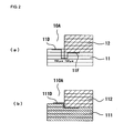
- a region, in which a conductive pattern of the external terminal electrodes 11D is not formed, is formed to be extended from the inside wall surface of the cavity 10A, which is used as the center, to a position 150 ⁇ m or more apart therefrom in every direction.
- a conductive pattern 111D may be cut off when a resin portion 111 and a ceramic multilayer substrate 112 are thermocompression-bonded, or wire breakage may occur by bending, resulting in conduction failure.
- the second chip type electronic components 14A and 14B are embedded in the resin portion 11 which is not necessarily to be fired, besides passive chip components, active chip components can be provided in the resin portion 11 as the second chip type electronic components 14A and 14B, and hence the enhancement of multifunctionality can be facilitated.
- a passive chip component such as a laminate capacitor or a laminate inductor
- an active chip component such as a semiconductor chip
- a resin forming a sealing resin portion 15 is preferably formed of a mixed resin composition containing a thermosetting resin and an inorganic filler.
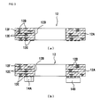
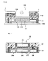
- a method for manufacturing the hybrid multilayer substrate 10 shown in Fig. 1 will be described with reference to Figs. 3 to 6.
- a method for forming a ceramic multilayer substrate 11 will be described.
- a slurry containing, for example, a low temperature sintered ceramic material is first applied on resin films made of PET or the like and is then dried, so that a predetermined number of ceramic green sheets having a thickness of approximately 10 to 200 ⁇ m are formed.
- a plurality of via conduction holes having a diameter of approximately 0.1 mm are formed in the ceramic green sheets to have a predetermined pattern.
- a conductive paste prepared by compounding a powdered metal primarily composed of Ag or Cu, a resin, and an organic solvent is filled in the via conduction holes in the ceramic green sheets, followed by drying, so that via conduction portions are formed.
- the same type conductive paste as described above is printed on the ceramic green sheet to form a predetermined pattern by a screen printing method, followed by drying, so that plane conduction portions used as a surface electrode and an in-plane conductor are formed.
- via conduction portions and plane conduction portions are formed in the other ceramic green sheets. Penetrating holes for the cavity 12B are formed in the above ceramic green sheets using a die, laser light, or the like.
- thermocompression bonding is performed at a predetermined pressure, such as 0.1 to 1.5 MPa, and at a temperature of 40 to 100°C, so that a green ceramic multilayer substrate having a penetrating hole for the cavity 10A is formed.
- This green ceramic multilayer substrate is fired, so that the ceramic multilayer substrate 12 having the penetrating hole 12B shown in Fig. 3(a) is obtained.
- a Ag-based conductive paste is used, the green ceramic multilayer substrate is fired in air at approximately 850°C, and when a Cu-based conductive paste is used, the green ceramic multilayer substrate is fired in an nitrogen gas at approximately 950°C.
- the ceramic multilayer substrate 12 After the ceramic multilayer substrate 12 is obtained, whenever necessary, films are formed, for example, by wet plating of Ni/Sn, Ni/Au, or the like on the surfaces of the external terminal electrodes 12C and 12D which are exposed at the top and the bottom surfaces of the ceramic multilayer substrate 12.
- films are formed, for example, by wet plating of Ni/Sn, Ni/Au, or the like on the surfaces of the external terminal electrodes 12C and 12D which are exposed at the top and the bottom surfaces of the ceramic multilayer substrate 12.
- the second chip type electronic components 14A and 14B are mounted on the ceramic multilayer substrate 12 with a bonding material, such as solder, provided therebetween as shown in Fig. 3(b).
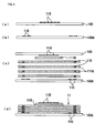
- the resin portion 11 is formed as shown in Fig. 4.
- the external terminal electrodes 11D located at the protrusion part 11B of the resin portion 11, that is, which is used as the bottom surface of the cavity 10A, and the external terminal electrodes 11C located at the bottom surface of the resin portion 11 are formed.
- a metal foil such as a copper foil, having a thickness of approximately 10 to 40 ⁇ m is adhered to a support 100 made of PET or the like as shown in Fig. 4(a)
- a resist layer is formed on the copper foil by applying a photoresist and is then exposed using a predetermined pattern, and subsequently an unnecessary resist layer is removed by development.
- the external terminal electrodes 11D are formed on the support 100 to have a predetermined pattern.
- the external terminal electrodes 11D are formed so as to be located in a region at least 150 ⁇ m apart from the periphery of the protrusion part 11B of the resin portion 11.
- the external terminal electrodes 11C are formed on a support 100A made of a PET or the like so as to have a predetermined pattern as shown in Fig. 4 (b).
- Via conduction holes having a predetermined pattern are formed in the resin sheets 111A using laser light or the like, and a conductive resin is filled in these via conduction holes, so that the via conductors 11E are formed.
- the external terminal electrodes 11D of the protrusion part 11B does not substantially shift in the horizontal direction, and as a result, a flat pattern can be formed almost as designed.
- a vacuum laminator or the like is preferably used as shown in Fig. 5(b) in which a flexible member or the like performs isotropic pressing in conformity with the shape of the laminate formed of the resin portion 11 and the ceramic multilayer substrate 12.
- a flat member support 100A
- a metal plate as shown in Fig. 5(b
- the resin portion 11 and the ceramic multilayer substrate 12 can be thermocompression-bonded.
- the external terminal electrodes 11D provided in the upper surface of the protrusion part 11B of the resin portion 11 are formed in a region at least 150 ⁇ m apart from the periphery of the protrusion part 11B, the external terminal electrodes 11D and the like may not be damaged.
- the protrusion part 11B of the resin portion 11 can be formed to have a plurality of steps.
- the first chip type electronic component 13 such as a semiconductor chip is mounted in the cavity 10A of the hybrid multilayer substrate 10'.
- the mounting surface for the first chip type electronic component 13 is formed from the resin to be flat without having any steps, and in addition, the external terminal electrodes 11D are not shifted, the posture of the first chip type electronic component 13 in the cavity 10A is stable, and hence the first chip type electronic component 13 can be reliably mounted with high accuracy without causing any connection failures and the like.
- flip chip connection chipping will not occur, and when reflow is performed, mounting can be performed with high accuracy by self-alignment.
- a resin is filled in a gap formed in the cavity 10A, and after the first chip type electronic component 13 is sealed as shown in Fig. 1(a), a predetermined heat treatment is performed, so that the sealing resin portion 15 is formed.
- the resin portion 11 having the protrusion part 11B and the ceramic multilayer substrate 12 having the penetrating hole 12B form a laminate structure
- the cavity 10A of the hybrid multilayer substrate 10 is formed by fitting the protrusion part 11B of the resin portion 11 to the bottom end part of the penetrating hole 12B of the ceramic multilayer substrate 12
- the bonding force between the resin portion 11 and the ceramic multilayer substrate 12 can be increased, and in addition, the external terminal electrodes 11D in the bottom surface of the cavity 10A can be formed almost as designed; hence, the hybrid multilayer substrate 10 can meet the trend toward reduction in size and increase in the number of pins of the first chip type electronic component 13, and the reliability as the hybrid multilayer substrate 10 can be improved.
- first chip type electronic component 13 is mounted in the cavity 10A, self-alignment mounting of the first chip type electronic component 13 can be performed.
- the bottom surface of the cavity 10A is planarized by the resin, the posture of the first chip type electronic component 13 is stable on the bottom surface used as the mounting surface, and hence electrical connection by wire bonding or the like can be reliably performed.
- flip-chip connection is performed for the first chip type electronic component 13 a plurality of connection terminals thereof can reliably reach the external terminal electrodes 11D in the protrusion part 11B and can be reliably connected thereto, and hence chipping and/or connection failures of flip-chip assembly and the like may not occur in mounting.
- the first chip type electronic component 13 since the first chip type electronic component 13 is placed in the cavity 10A, reduction in height of the hybrid multilayer substrate 10 can be realized. In addition, since the first chip type electronic component 13 placed in the cavity 10A is sealed by the sealing resin portion 15, the first chip type electronic component 13 can be protected from external mechanical shock, moisture, and the like, and hence the reliability can be improved.
- the ceramic multilayer substrate 12 is formed of the ceramic layers 12A laminated to each other, and conductive patterns formed of the external terminal electrodes 12C and 12D, the in-plane conductors 12E, and the via conductors 12F are provided in the ceramic multilayer substrate 12 and on the surfaces thereof, a region surrounding the first chip type electronic component 13 can be effectively used as a wiring region, and hence the reduction in height of the hybrid multilayer substrate 10 can be facilitated.
- the resin portion 11 has the external terminal electrodes 11C in the surface opposite to the surface bonded to the ceramic multilayer substrate 12, and the external terminal electrodes 11C are connected to the external terminal electrodes 12C, that is, to the conductive pattern formed on the ceramic multilayer substrate 12, via the via conductors 11E formed in the resin portion 11, the conductive pattern of the ceramic multilayer substrate 12 and the conductive pattern of the mounting substrate can be reliably connected to each other via the via conductors 11E of the resin portion 11, and as a result, the first and the second chip type electronic components 13, 14A, and 14B can be reliably connected to the mounting substrate, so that the enhancement of multifunctionality of the substrate can be realized.
- the ceramic multilayer substrate 12 is formed of the low temperature sintered ceramic layers 12A laminated to each other, and the conductive pattern thereof is formed of a conductive material primarily composed of silver or copper, the ceramic multilayer substrate 12 and the conductive pattern can be co-fired at a low temperature of 1,050°C or less, and hence even by the low temperature firing, a conductive pattern having low resistance can be reliably formed.
- the region, in which the conductive patterns of the external terminal electrodes 11D and the like are not provided at the interface between the resin portion 11 and the ceramic multilayer substrate 12 and on the bottom surface of the cavity 10A, is formed from the inside wall surface of the cavity 10A, which is used as the center, to a position 150 ⁇ m or more apart therefrom in every direction, moisture intrusion and connection defects may not occur, and hence a highly reliable conductive pattern can be formed.
- the hybrid multilayer substrate 10 when the hybrid multilayer substrate 10 is manufactured, there are provided respective steps for forming the resin portion 11 having the protrusion part 11B and for forming the ceramic multilayer substrate 12 having the penetrating hole 12B, and the step of bonding the resin portion 11 to the ceramic multilayer substrate 12 so as to fit the protrusion part 11B of the resin portion 11 to the end part of the penetrating hole 12B of the ceramic multilayer substrate 12. Accordingly, the resin portion 11 and the ceramic multilayer substrate 12 are united to form the cavity 10A in which the upper surface of the protrusion part 11B is used as the bottom surface. As a result, the hybrid multilayer substrate 10 can be reliably manufactured.
- a hybrid multilayer substrate 20 shown in Fig. 7 has a resin portion 21, a ceramic multilayer substrate 22, and first and second chip type electronic components 23, 24A, and 24B.
- a second chip type electronic component 24C is mounted in the resin portion 21 under the first chip type electronic component 23, so that a region of the resin portion 21 under the first chip type electronic component 23 is effectively used, and in addition, the second chip type electronic components 24A, 24B, and 24C are mounted to external terminal electrodes 21C formed in the bottom surface of the resin portion 21.
- the hybrid multilayer substrate 20 has the structure similar to that of the hybrid multilayer substrate 10 shown in Fig. 1. According to this embodiment, since the region of the resin portion 21 under the first chip type electronic component 23 can be effectively used for mounting the second chip type electronic component 24C, the multifunctionality can be enhanced as compared to the hybrid multilayer substrate 10 shown in Fig. 1.
- a hybrid multilayer substrate 30 shown in Fig. 8 has a resin portion 31, a ceramic multilayer substrate 32, and first and second chip type electronic components 33, 34A, and 34B.
- the hybrid multilayer substrate 30 of this embodiment has third chip type electronic components 37A and 37B mounted on the upper surface of the ceramic multilayer substrate 32 via external terminal electrodes 32D, and a second sealing resin portion 38 sealing the third chip type electronic components 37A and 37B.
- the hybrid multilayer substrate 30 has the structure similar to that of the hybrid multilayer substrate 10 shown in Fig. 1.
- the third chip type electronic components 37A and 37B for example, an active chip component, such as a semiconductor chip, and a passive chip component, such as a laminate capacitor or a laminate inductor, can be mounted.
- the hybrid multilayer substrate 30 can be obtained which has further enhanced multifunctionality.
- the third chip type electronic components 37A and 37B can be reliably protected from exterior moisture and the like.
- a hybridmultilayer substrate 40 shown in Fig. 9 has a resin portion 41, a ceramic multilayer substrate 42, and first and second chip type electronic components 43, 44A, and 44B.
- the hybrid multilayer substrate 40 of this embodiment has a second resin portion 48 formed on the bottom surface of the resin portion 41 and third chip type electronic components 47A and 47B provided in this second resin portion 48, and the resin portion 41 and the second resin portion 48 form a resin laminate. Except that the third chip type electronic components 47A and 47B and the second resin portion 48 are provided, the hybrid multilayer substrate 40 has the structure similar to that of the hybrid multilayer substrate 10 shown in Fig. 1.
- the resin portion 41 and the second resin portion 48 may contain the same resin component or may contain different resin components.
- the third chip type electronic component 47A is connected, for example, to external terminal electrodes 48D formed on an upper surface of the second resin portion 48, and the third chip type electronic component 47B is connected, for example, to external terminal electrodes 41C formed on a bottom surface of the resin portion 41.
- reference numeral 48E indicates a via conductor formed in the second resin portion 48, and this via conductor 48E connects between the via conductor 41E of the resin portion 41 and a mounting substrate.
- an active chip component such as a semiconductor chip
- a passive chip component such as a laminate capacitor or a laminate inductor
- a hybrid multilayer substrate 50 shown in Fig. 10 includes a resin portion 51, a ceramic multilayer substrate 52, and a first chip type electronic component 53, and has the structure similar to that of the hybrid multilayer substrate 10 shown in Fig. 1 except that the first chip type electronic component 53 is connected to external terminal electrodes 52D' of the ceramic multilayer substrate 52 via bonding wires 53A.
- a cavity 50A is formed so as to have a larger opening from a central part to the top of the inside wall surface along the height direction, and at a boundary part between the top and the bottom parts, a flat step 50B of the ceramic multilayer substrate 52 is formed.
- the external terminal electrodes 52D' are formed in the upper surface of this step 50B, and the external terminal electrodes 52D' are connected to the first chip type electronic component 53 via the bonding wires 53A.
- the bottom surface of the cavity 50A is formed by a protrusion part 51B of the resin portion 51 and is flat, the posture of the first chip type electronic component 53 in the cavity 50A is stable, and the first chip type electronic component 53 can be reliably connected to the external terminal electrodes 52D' of the ceramic multilayer substrate 52.
- effects and advantages similar to those of the hybrid multilayer substrates of the above embodiments can also be expected.
- the present invention is not limited to the above embodiments at all.
- the case in which the hybrid multilayer substrate is mounted on the mounting substrate with the resin portion provided therebetween has been described; however, the mounting can be performed using the ceramic substrate therebetween.
- the hybrid multilayer substrate 30 shown in Fig. 8 whenever necessary, either the top or the bottom surface of the hybrid multilayer substrate 30 can be connected to the mounting substrate.
- a hybrid multilayer substrate has a laminate structure made of a resin portion and a ceramic substrate and having a cavity
- the resin portion has a protrusion part
- the ceramic substrate has a penetrating hole
- the cavity is formed by fitting the protrusion part of the resin portion to an end part of the penetrating hole of the ceramic substrate
- the present invention can be preferably applied, for example, to a hybrid multilayer substrate used for various electronic apparatuses.
Landscapes
- Engineering & Computer Science (AREA)
- Microelectronics & Electronic Packaging (AREA)
- Manufacturing & Machinery (AREA)
- Production Of Multi-Layered Print Wiring Board (AREA)
Abstract
Description
- The present invention relates to hybrid multilayer substrates and methods for manufacturing the same, and more particularly, relates to a highly reliable hybrid multilayer substrate having a cavity in which an electronic component is mounted with high accuracy, and to a method for manufacturing the hybrid multilayer substrate.
- Heretofore, as this type of hybrid multilayer substrate, for example, a wiring substrate having a cavity disclosed in
Patent Document 1 may be mentioned. This wiring substrate is formed of a ceramic core substrate having a penetrating hole, a resin insulating layer which is formed on the bottom surface of this ceramic core substrate and which blocks up the penetrating hole to form a cavity, an IC chip mounted in the cavity formed by the resin insulating layer, and a filling material which is filled around the IC chip to seal it in the cavity. - When the above wiring substrate is manufactured, after the ceramic core substrate having a penetrating hole is formed, the IC chip is aligned in the penetrating hole of the ceramic core substrate, and the filling material is then filled in a gap between the IC chip and the penetrating hole so as to unite the IC chip and the ceramic core substrate in the penetrating hole. Next, by a conventional known method, a resin insulating layer having via holes is formed on the rear surface of the ceramic core substrate.
- Patent Document 1:
Japanese Unexamined Patent Application Publication No. 2003-309213 - However, as is the case of the wiring substrate disclosed in
Patent Document 1, since the resin insulating layer having via holes is formed for the IC chip fixed in the penetrating hole of the ceramic core substrate by the filling material, and a self-alignment function of the IC chip cannot be used in mounting, terminals of the IC chip and the via holes (electrodes) of the resin insulating layer cannot be easily disposed without causing any problems, and as a result, it is difficult to obtain electrical conduction between the IC chip and the electrodes formed in the resin insulating layer. Furthermore, since IC chips have been multifunctionalized in recent year, in ICs for flip-chip assembly, the pitch between terminals is decreased, the size of bumps is decreased, and the number of pins is increased; hence, as a result, it becomes increasingly difficult to obtain electrical conduction between the IC chip and the electrodes formed in the resin insulating layer. - In order to use the self-alignment function of the IC chip, it is necessary to form a
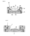
cavity 3 beforehand by thermocompression bonding of aresin insulating layer 2 havingelectrodes 2A to aceramic substrate 1 having a penetrating hole as shown in Fig. 11. Furthermore, concomitant with the increase in the number of pins because of the narrower pitch and smaller bumps of an IC chip, theelectrodes 2A must be formed with high accuracy in thecavity 3 so as to reduce the shift in position of theelectrodes 2A as small as possible. - However, as shown in Fig. 11, when the
resin insulating layer 2 is bonded to theceramic substrate 1 by thermocompression bonding, theresin insulating layer 2 flows during the thermocompression bonding, theelectrodes 2A located in thecavity 3 are shifted in the horizontal direction thereby, and hence it is difficult to form theelectrodes 2A with high accuracy. This tendency becomes apparent as the number of films which form theresin insulating layer 2 is increased, and as a result, the reliability of connection may not be ensured in some cases. - The present invention has been conceived in order to solve the problems described above, and an obj ect of the present invention is to provide a hybrid multilayer substrate and a method for manufacturing the same, the hybrid multilayer substrate having high arrangement accuracy of terminal electrodes and the like provided in the bottom surface of the cavity and being capable of significantly improving the reliability in connection with a mounted component.
- In accordance with
Claim 1 of the present invention, there is provided a method for manufacturing a hybrid multilayer substrate having a cavity in a laminate structure made of a resin portion and a ceramic substrate, which comprises the steps of: forming a resin portion having a protrusion part and a ceramic substrate having a penetrating hole; and bonding the resin portion to the ceramic substrate so as to fit the protrusion part of the resin portion to an end part of the penetrating hole of the ceramic substrate the resin portion. Accordingly, the ceramic substrate and the resin portion are united to form a cavity using an upper surface of the protrusion part as a bottom surface. - In addition, the method for manufacturing a hybrid multilayer substrate, which is described in
Claim 2 of the present invention, is in accordance withClaim 1 of the present invention, in which the resin portion and the ceramic substrate are compression-bonded to each other. - In addition, the method for manufacturing a hybrid multilayer substrate, which is described in
Claim 3 of the present invention, is in accordance withClaim - In addition, the method for manufacturing a hybrid multilayer substrate, which is described in Claim 4 of the present invention, is in accordance with
Claim 3 of the present invention, and further comprises the step of sealing the first chip type electronic component placed in the cavity with a resin. - In addition, the method for manufacturing a hybrid multilayer substrate, which is described in Claim 5 of the present invention, is in accordance with one of
Claims 1 to 4 of the present invention, in which the ceramic substrate is formed as a ceramic multilayer substrate composed of ceramic layers laminated to each other, and in which a predetermined conductive pattern is formed inside the ceramic multilayer substrate and on a surface thereof. - In addition, the method for manufacturing a hybrid multilayer substrate, which is described in Claim 6 of the present invention, is in accordance with Claim 5 of the present invention, in which the ceramic layers are formed using a low temperature sintered ceramic, and for the conductive pattern, a conductive material primarily composed of silver or copper is used.
- In addition, the method for manufacturing a hybrid multilayer substrate, which is described in Claim 7 of the present invention, is in accordance with Claim 5 or 6 of the present invention, in which a terminal electrode is formed in the surface of the resin portion opposite to the surface bonded to the ceramic multilayer substrate, and this terminal electrode is connected to the conductive pattern formed for the ceramic multilayer substrate via a via conductor formed in the resin portion.
- In addition, the method for manufacturing a hybrid multilayer substrate, which is described in Claim 8 of the present invention, is in accordance with one of
Claims 1 to 7 of the present invention, wherein a region, in which a conductive pattern is not formed at the interface between the resin portion and the ceramic substrate and on the bottom surface of the cavity, is formed to be extended from an inside wall surface of the cavity, which is used as the center, to aposition 150 µm or more apart therefrom in every direction. - In addition, the method for manufacturing a hybrid multilayer substrate, which is described in Claim 9 of the present invention, is in accordance with one of
Claims 3 to 8 of the present invention, and further comprises the step of placing a second chip type electronic component in the resin portion. - In addition, in accordance with
Claim 10 of the present invention, there is provided a hybrid multilayer substrate having a cavity in a laminate structure made of a resin portion and a ceramic substrate, in which the resin portion has a protrusion part and the ceramic substrate has a penetrating hole, and the cavity is formed of an upper surface of the protrusion part of the resin portion and a wall surface of the penetrating hole of the ceramic substrate. - In addition, the hybrid multilayer substrate described in
Claim 11 of the present invention is in accordance withClaim 10 of the present invention, in which a first chip type electronic component is placed in the cavity. - In addition, the hybrid multilayer substrate described in
Claim 12 of the present invention is in accordance withClaim 11 of the present invention, in which the first chip type electronic component placed in the cavity is sealed with a resin. - In addition, the hybrid multilayer substrate described in
Claim 13 of the present invention is in accordance with one ofClaims 10 to 12 of the present invention, in which the ceramic substrate is a ceramic multilayer substrate composed of ceramic layers laminated to each other, and a predetermined conductive pattern is formed inside the ceramic multilayer substrate and on a surface thereof. - In addition, the hybrid multilayer substrate described in Claim 14 of the present invention is in accordance with
Claim 13 of the present invention, in which the ceramic layers are each formed using a low temperature sintered ceramic layer, and the conductive pattern is formed of a conductive material primarily composed of silver or copper. - In addition, the hybrid multilayer substrate described in
Claim 15 of the present invention is in accordance withClaim 13 or 14 of the present invention, in which a terminal electrode is formed in the surface of the resin portion opposite to the surface bonded to the ceramic multilayer substrate, and the terminal electrode is connected to the conductive pattern formed for the ceramic multilayer substrate via a via conductor formed in the resin portion. - In addition, the hybrid multilayer substrate described in
Claim 16 of the present invention is in accordance with one ofClaims 13 to 15 of the present invention, wherein a region, in which a conductive pattern is not formed at the interface between the resin portion and the ceramic substrate and on the bottom surface of the cavity, is formed from an inside wall surface of the cavity, which is used as the center, to aposition 150 µm or more apart therefrom in every direction. - According to
Claims 1 to 16 of the present invention, a hybrid multilayer substrate and a method for manufacturing the same can be provided, the hybrid multilayer substrate having high arrangement accuracy of terminal electrodes and the like provided in the bottom surface of the cavity and being capable of significantly improving the reliability in connection with a mounted component. -
- Figs. 1(a) and 1(b) are views each showing one embodiment of a hybrid multilayer substrate according to the present invention; Fig. 1(a) is a cross-sectional view of the entire substrate; and Fig. 1(b) is a cross-sectional view showing the state before a chip type electronic component is sealed with a resin.
- Fig. 2 (a) and 2 (b) are views each illustrating an arrangement structure of electrodes provided in a bottom surface of a cavity formed in the hybrid multilayer substrate shown in Fig. 1.
- Figs. 3(a) and 3(b) are views each illustrating a step of mounting a chip type electronic component on a ceramic substrate of the hybrid multilayer substrate shown in Fig. 1.
- Figs. 4(a) to 4(d) are views each illustrating a step of forming a resin portion of the hybrid multilayer substrate shown in Fig. 1.
- Figs. 5(a) and 5(b) are views each illustrating a step of performing thermocompression bonding between a resin portion and a ceramic substrate of the hybrid multilayer substrate shown in Fig. 1.
- Fig. 6 is a view showing an important part of another manufacturing step of the hybrid multilayer substrate shown in Fig. 1.
- Fig. 7 is a cross-sectional view showing another embodiment of a hybrid multilayer substrate according to the present invention.
- Fig. 8 is a cross-sectional view showing still another embodiment of a hybrid multilayer substrate according to the present invention.
- Fig. 9 is a cross-sectional view showing still another embodiment of a hybrid multilayer substrate according to the present invention.
- Fig. 10 is a cross-sectional view showing still another embodiment of a hybrid multilayer substrate according to the present invention.
- Fig. 11 is a cross-sectional view showing a conventional multilayer substrate having a cavity before a chip type electronic component is mounted therein.
-
- 10, 20, 30, 40, 50 hybrid multilayer substrate
- 10A cavity
- 11, 21, 31, 41, 51 resin portion
- 11B protrusion part
- 11C external terminal electrode (terminal electrode)
- 11E via conductor
- 12, 22, 32, 42, 52 ceramic multilayer substrate (ceramic substrate)
- 12A ceramic layer
- 12B penetrating hole
- 12C external terminal electrode (conductive pattern)
- 12D external terminal electrode (conductive pattern)
- 12E in-plane conductor (conductive pattern)
- 12F via conductor (conductive pattern)
- 13, 23, 33, 43, 53 first chip type electronic component
- 14A, 24A, 34A, 44A second chip type electronic component
- 14B, 24B, 34B, 44B second chip type electronic component
- 15 sealing resin portion (resin)
- Hereinafter, the present invention will be described with reference to embodiments shown in Figs. 1 to 10.
- A
hybrid multilayer substrate 10 of this embodiment has, as shown in Fig. 1(a) by way of example, acavity 10A in a laminate structure which is formed of aresin portion 11 and aceramic substrate 12 laminated thereon, and is mounted on a mounting substrate (not shown) , such as a printed circuit board, with theresin portion 11 provided therebetween. In addition, when thehybrid multilayer substrate 10 is mounted on a ceramic-made substrate, mounting may be performed with theceramic substrate 12 provided therebetween. Since the mounting substrate, such as a printed circuit board, is made from a resin in many cases, theresin portion 11 is preferably formed of a resin having a thermal expansion coefficient between the thermal expansion coefficient of theceramic substrate 12 and that of the mounting substrate, such as an intermediate thermal expansion coefficient therebetween, or a resin having a thermal expansion coefficient gradient therebetween. Theresin portion 11 is present between theceramic substrate 12 and the mounting substrate to reduce the difference in thermal expansion between thehybrid multilayer substrate 10 and the mounting substrate, and as a result, thehybrid multilayer substrate 10 mounted on the mounting substrate is not easily removed therefrom even in a high temperature atmosphere. Thisresin portion 11 is formed to have a laminate structure composed ofresin layers 11A laminated to each other as shown in the figure, and theceramic substrate 12 is formed as a ceramic multilayer substrate includingceramic layers 12A laminated to each other. Hence, hereinafter, theceramic substrate 12 will be described as aceramic multilayer substrate 12. - Subsequently, as shown in Fig. 1(b), a
protrusion part 11B having a flat front surface is formed at a central part of the upper surface of theresin portion 11, and a penetratinghole 12B corresponding to theprotrusion part 11B of theresin portion 11 is formed in theceramic multilayer substrate 12. In addition, when theprotrusion part 11B of theresin portion 11 is fitted to a bottom end part of the penetratinghole 12B of theceramic multilayer substrate 12, theresin portion 11 and theceramic multilayer substrate 12 are united, so that thecavity 10A of thehybrid multilayer substrate 10 is formed. The height of theprotrusion part 11B may be at least 10 µm and is more preferably 50 µm or more. When the height of theprotrusion part 11B is more than 500 µm, since a protrusion region under the bottom surface of thecavity 10A is a useless region, the height of theprotrusion part 11B is preferably set to 500 µm or less. Since theprotrusion part 11B of theresin portion 11 is fitted to the bottom end part of the penetratinghole 12B of theceramic multilayer substrate 12, a bonding strength between theresin portion 11 and theceramic multilayer substrate 12 can be improved, and as a result, the reliability as thehybrid multilayer substrate 10 can be enhanced. - In the
cavity 10A, a first chip typeelectronic component 13 is provided. In addition, since second chip typeelectronic components ceramic substrate 12 are embedded in theresin portion 11, theresin portion 11 can be further effectively used as a mounting space for the second chip typeelectronic components hybrid multilayer substrate 10 can be increased so as to satisfy the trend toward enhancement of multifunctionality. - In addition, a resin is filled in the
cavity 10A, and by this resin, the first chip typeelectronic component 13 is sealed. This resin portion (hereinafter referred to as a "sealing resin portion") 15 has an upper surface flush with the upper surface of theceramic multilayer substrate 12, so that one flat surface is formed. As described above, since the first and the second chip typeelectronic components electronic components - Next, individual constituent elements of the
hybrid multilayer substrate 10 will be described in more detail. First, theresin portion 11 will be described. As shown in Figs. 1(a) and 1 (b) , externalterminal electrodes 11C are formed in the bottom surface of theresin portion 11 to have a predetermined pattern, and electrical connection to the mounting substrate is performed via the externalterminal electrodes 11C. Externalterminal electrodes 11D having a predetermined pattern are formed in the upper surface of theprotrusion part 11B of theresin portion 11 and are connected to the first chip typeelectronic component 13 placed in thecavity 10A. In addition, viaconductors 11E are provided in theresin portion 11 and serve to connect between a conductive pattern of theceramic multilayer substrate 12 and a conductive pattern of the mounting substrate. External terminal electrodes present at the bonding surface between theresin portion 11 and theceramic multilayer substrate 12 are not formed at theresin portion 11 side by the reason to be described below and are formed at theceramic multilayer substrate 12 side. - The
resin layer 11A is preferably formed from a mixed resin composition containing a thermosetting resin and an inorganic filler. As the thermosetting resin, for example, an epoxy resin, a phenol resin, or a cyanate resin, which has superior heat resistance and humidity resistance, may be used, and as the inorganic filler, for example, alumina, silica, or titania may be used. By addition of the inorganic filler as described above, the thermal expansion coefficient of theresin portion 11 can be adjusted, and heat dissipation properties thereof can also be improved. In addition, the fluidity of the resin can be appropriately controlled when theresin portion 11 is manufactured. - The external
terminal electrodes resin portion 11 are formed of a metal foil such as a copper foil. The viaconductor 11E is formed by filling a conductive resin in a via conduction hole formed in theresin portion 11. The conductive resin is a conductive resin composition formed, for example, of metal particles and a thermosetting resin. As the metal particles, for example, a metal, such as gold, silver, copper, or nickel, may be used, and as the thermosetting resin, for example, an epoxy resin, a phenol resin, or a cyanate resin may be used. In addition, whenever necessary, the viaconductor 11E may be formed, for example, of electroless plating copper and electrolytic plating copper. - Next, the
ceramicmultilayer substrate 12 will be described. As shown in Figs. 1(a) and 1(b), externalterminal electrodes 12C having a predetermined pattern is formed on the bottom surface of theceramic multilayer substrate 12, and theceramic multilayer substrate 12 is connected to the viaconductors 11E of theresin portion 11 via the externalterminal electrodes 12C. Externalterminal electrodes 12D having a predetermined pattern are formed in the upper surface of theceramic multilayer substrate 12, and a third chip type electronic component (not shown) can be mounted via theexternal terminal electrodes 12D. Furthermore, in-plane conductors 12E having a predetermined pattern are formed in the individualceramic layers 12A of theceramic multilayer substrate 12, and the in-plane conductors 12E adjacent in an up and down direction are connected to each other viaconductors 12F having a predetermined pattern. The externalterminal electrodes plane conductors 12E, and the viaconductors 12F are connected to each other, so that a conductive pattern of theceramic multilayer substrate 12 is formed. - The
ceramic layer 12A is formed of a ceramic material. Although the ceramic material is not particularly limited, for example, a low temperature sintered ceramic (LTCC:Low Temperature Co-fired Ceramic) material may be preferably used. The low temperature sintered ceramic is a ceramic material which can be fired at a temperature of 1, 050°C or less. As the low temperature sintered ceramic material, for example, there may be mentioned a glass composite-based LTCC material containing powdered ceramic, such asalumina,forsterite, orcordierite, andborosilicateglass mixed therewith; a crystalline glass-based LTCC material using a ZnO-MgO-Al2O3-SiO2-based crystalline glass; or a non-glass-based LTCC material using a powdered BaO-Al2O3-SiO2-based ceramic, a powdered Al2O3-CaO-SiO2-MgO-B2O3-based ceramic, or the like. - When a low temperature sintered ceramic material is used for the
ceramic multilayer substrate 12, as a conductive material for the externalterminal electrodes ceramic layers 12A so as to be united therewith. Hence, the conductive patterns of the externalterminal electrodes ceramic multilayer substrate 12. - Since the
ceramic multilayer substrate 12 is formed of a low temperature sintered ceramic material as described above and has a surface roughness Rmax (several micrometers) approximately equivalent to that of a copper foil, the bonding force to theresin portion 11 is not strong. Hence, in this embodiment, the externalterminal electrode 12C connecting between theceramic multilayer substrate 12 and theresin portion 11 is formed of a sintered metal as described above. The sintered metal forming the externalterminal electrode 12C has a surface roughness Rmax of several tens of micrometers, which is larger by one order of magnitude than that of a copper foil which has a surface roughness Rmax of several micrometers, and hence the bonding force to theresin portion 11 can be increased by an anchor effect of the sintered metal. The difference in surface roughness as described above is because of the following reason. The copper foil is formed by plating or rolling of a copper sheet, and on the other hand, the sinteredmetal is formed by firing a conductive paste containing 10% to 40% of a resin component on a volume ratio basis; hence, the resin component is burned out to form voids inside or on the surface, and as a result, the surface roughness is increased. - The first chip type
electronic component 13 is placed on and connected to theexternal terminal electrodes 11D formed in the upper surface of theprotrusion part 11B of theresin portion 11 viasolder balls 16. Since theprotrusion part 11B of theresin portion 11 is fitted in the penetratinghole 12B of theceramic multilayer substrate 12, when theresin portion 11 and theceramic multilayer substrate 12 are thermocompression-bonded together, theprotrusion part 11B is held by the penetratinghole 12B so that the flow of the resin of theprotrusion part 11B is prevented or suppressed, and as a result, the shift in position of theexternal terminal electrodes 11D formed in the upper surface of theprotrusion part 11B can be prevented or suppressed as small as possible. Hence, theexternal terminal electrodes 11D located at a mounting surface for the first chip typeelectronic component 13 can be formed almost as designed to be disposed with high accuracy. As the first chip typeelectronic component 13, for example, an active chip component, such as a semiconductor chip, or a passive chip component, such as a laminate capacitor or a laminate inductor, may be provided. - In addition, as shown in Fig. 2 (a), at the interface between the
resin portion 11 and theceramic multilayer substrate 12 and on the bottom surface of thecavity 10A, a region, in which a conductive pattern of theexternal terminal electrodes 11D is not formed, is formed to be extended from the inside wall surface of thecavity 10A, which is used as the center, to aposition 150 µm or more apart therefrom in every direction. As shown in Fig. 2(b), when it is assumed that a conductive pattern is continuously formed in an area extended from the inside wall surface of acavity 110A, which is used as the center, to a position less than 150 µm apart therefrom in every direction, aconductive pattern 111D may be cut off when aresin portion 111 and aceramic multilayer substrate 112 are thermocompression-bonded, or wire breakage may occur by bending, resulting in conduction failure. In addition, as shown in Fig. 2 (a), when it is assumed that aconductive pattern 11F of theresin portion 11 is present at the interface between theresin portion 11 and theceramic multilayer substrate 12, since theconductive pattern 11F of theresin portion 11 is formed from a copper foil, the bonding force between theresin portion 11 and theceramic multilayer substrate 12 is decreased, and in addition, moisture is liable to enter through the interface between theportion 11 and thesubstrate 12; hence, the reliability may be degraded in some cases. - In addition, since the second chip type
electronic components resin portion 11 which is not necessarily to be fired, besides passive chip components, active chip components can be provided in theresin portion 11 as the second chip typeelectronic components electronic component 14A, for example, a passive chip component, such as a laminate capacitor or a laminate inductor, is provided, and as the second chip typeelectronic component 14B, for example, an active chip component, such as a semiconductor chip, is provided. - In addition, as is the case of the
resin portion 11, a resin forming a sealingresin portion 15 is preferably formed of a mixed resin composition containing a thermosetting resin and an inorganic filler. - Next, a method for manufacturing the
hybrid multilayer substrate 10 shown in Fig. 1 will be described with reference to Figs. 3 to 6. First, a method for forming aceramic multilayer substrate 11 will be described. A slurry containing, for example, a low temperature sintered ceramic material is first applied on resin films made of PET or the like and is then dried, so that a predetermined number of ceramic green sheets having a thickness of approximately 10 to 200 µm are formed. - Next, by using a die or laser light, a plurality of via conduction holes having a diameter of approximately 0.1 mm are formed in the ceramic green sheets to have a predetermined pattern. In addition, for example, a conductive paste prepared by compounding a powdered metal primarily composed of Ag or Cu, a resin, and an organic solvent is filled in the via conduction holes in the ceramic green sheets, followed by drying, so that via conduction portions are formed. Furthermore, the same type conductive paste as described above is printed on the ceramic green sheet to form a predetermined pattern by a screen printing method, followed by drying, so that plane conduction portions used as a surface electrode and an in-plane conductor are formed. In the same manner as described above, via conduction portions and plane conduction portions are formed in the other ceramic green sheets. Penetrating holes for the
cavity 12B are formed in the above ceramic green sheets using a die, laser light, or the like. - Next, after a predetermined number of the ceramic green sheets formed as described above are laminated to each other, thermocompression bonding is performed at a predetermined pressure, such as 0.1 to 1.5 MPa, and at a temperature of 40 to 100°C, so that a green ceramic multilayer substrate having a penetrating hole for the
cavity 10A is formed. This green ceramic multilayer substrate is fired, so that theceramic multilayer substrate 12 having the penetratinghole 12B shown in Fig. 3(a) is obtained. When a Ag-based conductive paste is used, the green ceramic multilayer substrate is fired in air at approximately 850°C, and when a Cu-based conductive paste is used, the green ceramic multilayer substrate is fired in an nitrogen gas at approximately 950°C. After theceramic multilayer substrate 12 is obtained, whenever necessary, films are formed, for example, by wet plating of Ni/Sn, Ni/Au, or the like on the surfaces of the externalterminal electrodes ceramic multilayer substrate 12. By the sequential steps described above, theceramic multilayer substrate 12 shown in Fig. 3(a) is obtained. - Subsequently, after the external
terminal electrodes 12C on the bottom surface of theceramic multilayer substrate 12 and the second chip typeelectronic components electronic components ceramic multilayer substrate 12 with a bonding material, such as solder, provided therebetween as shown in Fig. 3(b). - In addition, the
resin portion 11 is formed as shown in Fig. 4. Theexternal terminal electrodes 11D located at theprotrusion part 11B of theresin portion 11, that is, which is used as the bottom surface of thecavity 10A, and the externalterminal electrodes 11C located at the bottom surface of theresin portion 11 are formed. For this formation, after a metal foil, such as a copper foil, having a thickness of approximately 10 to 40 µm is adhered to asupport 100 made of PET or the like as shown in Fig. 4(a), a resist layer is formed on the copper foil by applying a photoresist and is then exposed using a predetermined pattern, and subsequently an unnecessary resist layer is removed by development. Then, after an unnecessary copper foil portion is removed by an etching treatment, a resist film is peeled away, so that as shown in the above figure, theexternal terminal electrodes 11D are formed on thesupport 100 to have a predetermined pattern. Theexternal terminal electrodes 11D are formed so as to be located in a region at least 150 µm apart from the periphery of theprotrusion part 11B of theresin portion 11. In addition, in a manner similar to that described above, the externalterminal electrodes 11C are formed on asupport 100A made of a PET or the like so as to have a predetermined pattern as shown in Fig. 4 (b). - Next, as shown in Fig. 4 (c), a predetermined number of
resin sheets 111A in a prepreg state obtained by mixing a thermosetting resin, such as an epoxy resin, and an inorganic filler, such as alumina, are formed, and in addition, aresin sheet 111B to be formed into theprotrusion part 11B is also formed. Via conduction holes having a predetermined pattern are formed in theresin sheets 111A using laser light or the like, and a conductive resin is filled in these via conduction holes, so that the viaconductors 11E are formed. Subsequently, as shown in Fig. 4(c), after asupport 110A having the externalterminal electrodes 11C, a predetermined number of theresin sheets 111A having the viaconductors 11E, theresin sheet 111B, and thesupport 100 having theexternal terminal electrodes 11D are laminated in that order while alignment therebetween is being performed, compression bonding is performed at a predetermined pressure, followed by removing thesupport 100. Accordingly, as shown in Fig. 4(d), theexternal terminal electrodes 11D on thesupport 100 are transferred to theresin sheet 111B, and hence theresin portion 11 having theprotrusion part 11B can be obtained. - Subsequently, as shown in Fig. 5(a), when the penetrating
hole 12B of theceramic multilayer substrate 12 and theprotrusion part 11B of theresin portion 11 are aligned at the upper side of theresin portion 11 provided on thesupport 100A and are then thermocompression-bonded at a thermosetting temperature of the resin, theprotrusion part 11B is fitted to the penetratinghole 12B, and in addition, the second chip typeelectronic components resin portion 11. In this step, since theprotrusion part 11B is held by the penetratinghole 12B, the resin forming theprotrusion part 11B substantially does not flow, and a resin other than that of theprotrusion part 11B flows and forms theresin portion 11. Hence, theexternal terminal electrodes 11D of theprotrusion part 11B does not substantially shift in the horizontal direction, and as a result, a flat pattern can be formed almost as designed. When the thermocompression bonding is performed, a vacuum laminator or the like is preferably used as shown in Fig. 5(b) in which a flexible member or the like performs isotropic pressing in conformity with the shape of the laminate formed of theresin portion 11 and theceramic multilayer substrate 12. When the isotropic pressing is performed, by supporting the laminate by a flat member (support 100A) such as a metal plate as shown in Fig. 5(b), a hybrid multilayer substrate 10' can be obtained which has superior flatness and which is made of theresin portion 11 and theceramic multilayer substrate 12. - In addition, when a
press mold 200 having aprotrusion part 200A is used as shown in Fig. 6 instead of the isotropic pressing, and when pressing is performed while theprotrusion part 200A is fitted to the penetratinghole 12B of theceramic multilayer substrate 12, theresin portion 11 and theceramic multilayer substrate 12 can be thermocompression-bonded. In this step, since theexternal terminal electrodes 11D provided in the upper surface of theprotrusion part 11B of theresin portion 11 are formed in a region at least 150 µm apart from the periphery of theprotrusion part 11B, theexternal terminal electrodes 11D and the like may not be damaged. In addition, when a multistage press mold having a plurality of protrusion steps is used as the press mold, theprotrusion part 11B of theresin portion 11 can be formed to have a plurality of steps. - Next, the first chip type
electronic component 13 such as a semiconductor chip is mounted in thecavity 10A of the hybrid multilayer substrate 10'. In this step, since the mounting surface for the first chip typeelectronic component 13 is formed from the resin to be flat without having any steps, and in addition, theexternal terminal electrodes 11D are not shifted, the posture of the first chip typeelectronic component 13 in thecavity 10A is stable, and hence the first chip typeelectronic component 13 can be reliably mounted with high accuracy without causing any connection failures and the like. In addition, when flip chip connection is performed, chipping will not occur, and when reflow is performed, mounting can be performed with high accuracy by self-alignment. - After the first chip type
electronic component 13 is mounted, a resin is filled in a gap formed in thecavity 10A, and after the first chip typeelectronic component 13 is sealed as shown in Fig. 1(a), a predetermined heat treatment is performed, so that the sealingresin portion 15 is formed. - As described above, according to this embodiment, since the
resin portion 11 having theprotrusion part 11B and theceramic multilayer substrate 12 having the penetratinghole 12B form a laminate structure, and thecavity 10A of thehybrid multilayer substrate 10 is formed by fitting theprotrusion part 11B of theresin portion 11 to the bottom end part of the penetratinghole 12B of theceramic multilayer substrate 12, the bonding force between theresin portion 11 and theceramic multilayer substrate 12 can be increased, and in addition, theexternal terminal electrodes 11D in the bottom surface of thecavity 10A can be formed almost as designed; hence, thehybrid multilayer substrate 10 can meet the trend toward reduction in size and increase in the number of pins of the first chip typeelectronic component 13, and the reliability as thehybrid multilayer substrate 10 can be improved. In addition, since the first chip typeelectronic component 13 is mounted in thecavity 10A, self-alignment mounting of the first chip typeelectronic component 13 can be performed. In addition, since the bottom surface of thecavity 10A is planarized by the resin, the posture of the first chip typeelectronic component 13 is stable on the bottom surface used as the mounting surface, and hence electrical connection by wire bonding or the like can be reliably performed. Also in the case in which flip-chip connection is performed for the first chip typeelectronic component 13, a plurality of connection terminals thereof can reliably reach theexternal terminal electrodes 11D in theprotrusion part 11B and can be reliably connected thereto, and hence chipping and/or connection failures of flip-chip assembly and the like may not occur in mounting. - In addition, according to this embodiment, since the first chip type
electronic component 13 is placed in thecavity 10A, reduction in height of thehybrid multilayer substrate 10 can be realized. In addition, since the first chip typeelectronic component 13 placed in thecavity 10A is sealed by the sealingresin portion 15, the first chip typeelectronic component 13 can be protected from external mechanical shock, moisture, and the like, and hence the reliability can be improved. Since theceramic multilayer substrate 12 is formed of theceramic layers 12A laminated to each other, and conductive patterns formed of the externalterminal electrodes plane conductors 12E, and the viaconductors 12F are provided in theceramic multilayer substrate 12 and on the surfaces thereof, a region surrounding the first chip typeelectronic component 13 can be effectively used as a wiring region, and hence the reduction in height of thehybrid multilayer substrate 10 can be facilitated. - In addition, since the
resin portion 11 has the externalterminal electrodes 11C in the surface opposite to the surface bonded to theceramic multilayer substrate 12, and the externalterminal electrodes 11C are connected to the externalterminal electrodes 12C, that is, to the conductive pattern formed on theceramic multilayer substrate 12, via the viaconductors 11E formed in theresin portion 11, the conductive pattern of theceramic multilayer substrate 12 and the conductive pattern of the mounting substrate can be reliably connected to each other via the viaconductors 11E of theresin portion 11, and as a result, the first and the second chip typeelectronic components - In addition, according to this embodiment, since the
ceramic multilayer substrate 12 is formed of the low temperature sinteredceramic layers 12A laminated to each other, and the conductive pattern thereof is formed of a conductive material primarily composed of silver or copper, theceramic multilayer substrate 12 and the conductive pattern can be co-fired at a low temperature of 1,050°C or less, and hence even by the low temperature firing, a conductive pattern having low resistance can be reliably formed. - In addition, since the region, in which the conductive patterns of the
external terminal electrodes 11D and the like are not provided at the interface between theresin portion 11 and theceramic multilayer substrate 12 and on the bottom surface of thecavity 10A, is formed from the inside wall surface of thecavity 10A, which is used as the center, to aposition 150 µm or more apart therefrom in every direction, moisture intrusion and connection defects may not occur, and hence a highly reliable conductive pattern can be formed. - In addition, according to this embodiment, when the
hybrid multilayer substrate 10 is manufactured, there are provided respective steps for forming theresin portion 11 having theprotrusion part 11B and for forming theceramic multilayer substrate 12 having the penetratinghole 12B, and the step of bonding theresin portion 11 to theceramic multilayer substrate 12 so as to fit theprotrusion part 11B of theresin portion 11 to the end part of the penetratinghole 12B of theceramic multilayer substrate 12. Accordingly, theresin portion 11 and theceramic multilayer substrate 12 are united to form thecavity 10A in which the upper surface of theprotrusion part 11B is used as the bottom surface. As a result, thehybrid multilayer substrate 10 can be reliably manufactured. - Next, other embodiments of the hybrid multilayer substrate according to the present invention will be described with reference to Figs. 7 to 10. In the following description, characteristic portions of the embodiments will be each described using a reference numeral which is increased by 10 in each embodiment.
- As is the
hybrid multilayer substrate 10 shown in Fig. 1, ahybrid multilayer substrate 20 shown in Fig. 7 has aresin portion 21, aceramic multilayer substrate 22, and first and second chip typeelectronic components electronic component 24C is mounted in theresin portion 21 under the first chip typeelectronic component 23, so that a region of theresin portion 21 under the first chip typeelectronic component 23 is effectively used, and in addition, the second chip typeelectronic components terminal electrodes 21C formed in the bottom surface of theresin portion 21. Except for the above two points described above, thehybrid multilayer substrate 20 has the structure similar to that of thehybrid multilayer substrate 10 shown in Fig. 1. According to this embodiment, since the region of theresin portion 21 under the first chip typeelectronic component 23 can be effectively used for mounting the second chip typeelectronic component 24C, the multifunctionality can be enhanced as compared to thehybrid multilayer substrate 10 shown in Fig. 1. - As is the
hybrid multilayer substrate 10 shown in Fig. 1, ahybrid multilayer substrate 30 shown in Fig. 8 has aresin portion 31, aceramic multilayer substrate 32, and first and second chip typeelectronic components hybrid multilayer substrate 30 of this embodiment has third chip typeelectronic components ceramic multilayer substrate 32 viaexternal terminal electrodes 32D, and a secondsealing resin portion 38 sealing the third chip typeelectronic components hybrid multilayer substrate 30 has the structure similar to that of thehybrid multilayer substrate 10 shown in Fig. 1. As the third chip typeelectronic components - According to this embodiment, since the third chip type
electronic components ceramic multilayer substrate 32, compared to the case of the above embodiment, thehybrid multilayer substrate 30 can be obtained which has further enhanced multifunctionality. In addition, since being covered with the secondsealing resin portion 38, the third chip typeelectronic components - As is the
hybrid multilayer substrate 10 shown in Fig. 1, ahybridmultilayer substrate 40 shown in Fig. 9 has aresin portion 41, aceramic multilayer substrate 42, and first and second chip typeelectronic components hybrid multilayer substrate 40 of this embodiment has asecond resin portion 48 formed on the bottom surface of theresin portion 41 and third chip typeelectronic components second resin portion 48, and theresin portion 41 and thesecond resin portion 48 form a resin laminate. Except that the third chip typeelectronic components second resin portion 48 are provided, thehybrid multilayer substrate 40 has the structure similar to that of thehybrid multilayer substrate 10 shown in Fig. 1. For example, theresin portion 41 and thesecond resin portion 48 may contain the same resin component or may contain different resin components. The third chip typeelectronic component 47A is connected, for example, to externalterminal electrodes 48D formed on an upper surface of thesecond resin portion 48, and the third chip typeelectronic component 47B is connected, for example, to external terminal electrodes 41C formed on a bottom surface of theresin portion 41. In this figure,reference numeral 48E indicates a via conductor formed in thesecond resin portion 48, and this viaconductor 48E connects between the viaconductor 41E of theresin portion 41 and a mounting substrate. As the third chip typeelectronic components hybrid multilayer substrate 30 shown in Fig. 8 can also be expected. - In addition, a
hybrid multilayer substrate 50 shown in Fig. 10 includes aresin portion 51, aceramic multilayer substrate 52, and a first chip typeelectronic component 53, and has the structure similar to that of thehybrid multilayer substrate 10 shown in Fig. 1 except that the first chip typeelectronic component 53 is connected to externalterminal electrodes 52D' of theceramic multilayer substrate 52 viabonding wires 53A. In this embodiment, acavity 50A is formed so as to have a larger opening from a central part to the top of the inside wall surface along the height direction, and at a boundary part between the top and the bottom parts, aflat step 50B of theceramic multilayer substrate 52 is formed. In addition, theexternal terminal electrodes 52D' are formed in the upper surface of thisstep 50B, and theexternal terminal electrodes 52D' are connected to the first chip typeelectronic component 53 via thebonding wires 53A. Also in this embodiment, since the bottom surface of thecavity 50A is formed by aprotrusion part 51B of theresin portion 51 and is flat, the posture of the first chip typeelectronic component 53 in thecavity 50A is stable, and the first chip typeelectronic component 53 can be reliably connected to theexternal terminal electrodes 52D' of theceramic multilayer substrate 52. In this embodiment, effects and advantages similar to those of the hybrid multilayer substrates of the above embodiments can also be expected. - The present invention is not limited to the above embodiments at all. For example, in the above embodiments, the case in which the hybrid multilayer substrate is mounted on the mounting substrate with the resin portion provided therebetween has been described; however, the mounting can be performed using the ceramic substrate therebetween. For example, in the case of the
hybrid multilayer substrate 30 shown in Fig. 8, whenever necessary, either the top or the bottom surface of thehybrid multilayer substrate 30 can be connected to the mounting substrate. That is, when a hybrid multilayer substrate has a laminate structure made of a resin portion and a ceramic substrate and having a cavity, the resin portion has a protrusion part, the ceramic substrate has a penetrating hole, and the cavity is formed by fitting the protrusion part of the resin portion to an end part of the penetrating hole of the ceramic substrate, the above hybrid multilayer substrate is included in the present invention. - The present invention can be preferably applied, for example, to a hybrid multilayer substrate used for various electronic apparatuses.
Claims (16)
- A method for manufacturing a hybrid multilayer substrate having a cavity in a laminate structure made of a resin portion and a ceramic substrate, comprising the steps of:forming a resin portion having a protrusion part and a ceramic substrate having a penetrating hole; andbonding the resin portion to the ceramic substrate so as to fit the protrusion part of the resin portion to an end part of the penetrating hole of the ceramic substrate, whereby the ceramic substrate and the resin portion are united to form a cavity which uses an upper surface of the protrusion part as a bottom surface.
- The method for manufacturing a hybrid multilayer substrate according to Claim 1, wherein the resin portion and the ceramic substrate are compression-bonded to each other.
- The method for manufacturing a hybrid multilayer substrate according to Claim 1 or 2, further comprising the step of placing a first chip type electronic component in the cavity.
- The method for manufacturing a hybrid multilayer substrate according to Claim 3, further comprising the step of sealing the first chip type electronic component placed in the cavity with a resin.
- The method for manufacturing a hybrid multilayer substrate according to one of Claims 1 to 4, wherein the ceramic substrate is formed as a ceramic multilayer substrate composed of ceramic layers laminated to each other, and a predetermined conductive pattern is formed inside the ceramic multilayer substrate and on a surface thereof.
- The method for manufacturing a hybrid multilayer substrate according to Claim 5, wherein the ceramic layers are formed using a low temperature sintered ceramic, and as the conductive pattern, a conductive material primarily composed of silver or copper is used.
- The method for manufacturing a hybrid multilayer substrate according to Claim 5 or 6, wherein a terminal electrode is formed in the surface of the resin portion opposite to the surface bonded to the ceramic multilayer substrate, and this terminal electrode is connected to the conductive pattern formed for the ceramic multilayer substrate via a via conductor formed in the resin portion.
- The method for manufacturing a hybrid multilayer substrate according to one of Claims 1 to 7, wherein a region, in which a conductive pattern is not formed at the interface between the resin portion and the ceramic substrate and on the bottom surface of the cavity, is formed to be extended from an inside wall surface of the cavity, which is used as the center, to a position 150 µm or more apart therefrom in every direction.
- The method for manufacturing a hybrid multilayer substrate according to one of Claims 3 to 8, further comprising the step of placing a second chip type electronic component in the resin portion.
- A hybrid multilayer substrate having a cavity in a laminate structure made of a resin portion and a ceramic substrate,
wherein the resin portion has a protrusion part and the ceramic substrate has a penetrating hole, and
the cavity is formed of an upper surface of the protrusion part of the resin portion and a wall surface of the penetrating hole of the ceramic substrate. - The hybrid multilayer substrate according to Claim 10, wherein a first chip type electronic component is placed in the cavity.
- The hybrid multilayer substrate according to Claim 11, wherein the first chip type electronic component placed in the cavity is sealed with a resin.
- The hybrid multilayer substrate according to one of Claims 10 to 12, wherein the ceramic substrate is a ceramic multilayer substrate composed of ceramic layers laminated to each other, and a predetermined conductive pattern is formed inside the ceramic multilayer substrate and on a surface thereof.
- The hybrid multilayer substrate according to Claim 13, wherein the ceramic layers are each formed using a low temperature sintered ceramic layer, and the conductive pattern is formed of a conductive material primarily composed of silver or copper.
- The hybrid multilayer substrate according to Claim 13 or 14, wherein a terminal electrode is formed in the surface of the resin portion opposite to the surface bonded to the ceramic multilayer substrate, and the terminal electrode is connected to the conductive pattern formed for the ceramic multilayer substrate via a via conductor formed in the resin portion.
- The hybrid multilayer substrate according to one of Claims 13 to 15, wherein a region, in which a conductive pattern is not formed at the interface between the resin portion and the ceramic substrate and on the bottom surface of the cavity, is formed from an inside wall surface of the cavity, which is used as the center, to a position 150 µm or more apart therefrom in every direction.
Applications Claiming Priority (2)
| Application Number | Priority Date | Filing Date | Title |
|---|---|---|---|
| JP2004308322 | 2004-10-22 | ||
| PCT/JP2005/018937 WO2006043474A1 (en) | 2004-10-22 | 2005-10-14 | Composite multilayer substrate and its manufacturing method |
Publications (3)
| Publication Number | Publication Date |
|---|---|
| EP1804562A1 true EP1804562A1 (en) | 2007-07-04 |
| EP1804562A4 EP1804562A4 (en) | 2011-01-26 |
| EP1804562B1 EP1804562B1 (en) | 2012-10-17 |
Family
ID=36202890
Family Applications (1)
| Application Number | Title | Priority Date | Filing Date |
|---|---|---|---|
| EP05793224A Expired - Lifetime EP1804562B1 (en) | 2004-10-22 | 2005-10-14 | Composite multilayer substrate and its manufacturing method |
Country Status (5)
| Country | Link |
|---|---|
| US (1) | US7488897B2 (en) |
| EP (1) | EP1804562B1 (en) |
| JP (1) | JP4310467B2 (en) |
| CN (1) | CN100508701C (en) |
| WO (1) | WO2006043474A1 (en) |
Cited By (1)
| Publication number | Priority date | Publication date | Assignee | Title |
|---|---|---|---|---|
| EP1936676A3 (en) * | 2006-12-22 | 2015-02-25 | TDK Corporation | Method of mounting electronic components, method of manufacturing an electronic component-embedded substrate, and electronic component-embedded substrate |
Families Citing this family (41)
| Publication number | Priority date | Publication date | Assignee | Title |
|---|---|---|---|---|
| CN101315925A (en) * | 2007-05-28 | 2008-12-03 | 松下电器产业株式会社 | Electronic device built-in module and manufacturing method thereof |
| TWM335792U (en) * | 2007-08-16 | 2008-07-01 | Aflash Technology Co Ltd | Device structure of IC |
| KR100896609B1 (en) * | 2007-10-31 | 2009-05-08 | 삼성전기주식회사 | Manufacturing method of multilayer ceramic substrate |
| JP5154262B2 (en) * | 2008-02-26 | 2013-02-27 | 太陽誘電株式会社 | Electronic components |
| KR101037695B1 (en) * | 2008-12-10 | 2011-05-30 | 주식회사 하이닉스반도체 | Copper Clad Laminated Plate with Capacitor, Printed Circuit Board Using Same and Semiconductor Package Using Same |
| JP4998503B2 (en) * | 2009-04-07 | 2012-08-15 | パナソニック株式会社 | Electronic component mounting system and electronic component mounting method |
| US8299366B2 (en) * | 2009-05-29 | 2012-10-30 | Ibiden Co., Ltd. | Wiring board and method for manufacturing the same |
| US8461462B2 (en) * | 2009-09-28 | 2013-06-11 | Kyocera Corporation | Circuit substrate, laminated board and laminated sheet |
| US9485877B2 (en) | 2009-09-28 | 2016-11-01 | Kyocera Corporation | Structure for circuit board used in electronic devices and method for manufacturing the same |
| WO2011148915A1 (en) * | 2010-05-26 | 2011-12-01 | 株式会社村田製作所 | Module substrate and method for manufacturing same |
| KR101289140B1 (en) * | 2010-09-28 | 2013-07-23 | 삼성전기주식회사 | Embedded substrate and a method for manufacturing the same |
| US9077344B2 (en) * | 2010-12-07 | 2015-07-07 | Atmel Corporation | Substrate for electrical component and method |
| CN103052281A (en) * | 2011-10-14 | 2013-04-17 | 富葵精密组件(深圳)有限公司 | Embedded multilayer circuit board and manufacturing method thereof |
| US20130229777A1 (en) * | 2012-03-01 | 2013-09-05 | Infineon Technologies Ag | Chip arrangements and methods for forming a chip arrangement |
| KR102042033B1 (en) * | 2012-10-30 | 2019-11-08 | 엘지이노텍 주식회사 | Printed circuit board for mounting chip and manufacturing method thereof |
| KR101561188B1 (en) * | 2013-02-20 | 2015-10-16 | 에스케이이노베이션 주식회사 | Anode for lithium secondary battery, fabricating method thereof and lithium air battery having the same |
| JP5692473B1 (en) * | 2013-05-14 | 2015-04-01 | 株式会社村田製作所 | Component built-in board and communication module |
| US9190389B2 (en) | 2013-07-26 | 2015-11-17 | Infineon Technologies Ag | Chip package with passives |
| US9070568B2 (en) * | 2013-07-26 | 2015-06-30 | Infineon Technologies Ag | Chip package with embedded passive component |
| JP2015035496A (en) * | 2013-08-09 | 2015-02-19 | イビデン株式会社 | Method of manufacturing electronic component built-in wiring board |
| JP5412002B1 (en) * | 2013-09-12 | 2014-02-12 | 太陽誘電株式会社 | Component built-in board |
| JP5846187B2 (en) * | 2013-12-05 | 2016-01-20 | 株式会社村田製作所 | Built-in module |
| KR102158068B1 (en) * | 2014-02-05 | 2020-09-21 | 엘지이노텍 주식회사 | Embedded printed circuit substrate |
| KR102281458B1 (en) * | 2014-06-23 | 2021-07-27 | 삼성전기주식회사 | Printed circuit board having an embedded device, semiconductor package and method of manufacturing the same |
| CN106463515B (en) * | 2014-06-25 | 2020-01-14 | 京瓷株式会社 | Substrate for mounting imaging element and imaging device |
| JP5797309B1 (en) | 2014-07-22 | 2015-10-21 | 株式会社フジクラ | Printed wiring board |
| DE102014112678A1 (en) | 2014-09-03 | 2016-03-03 | Epcos Ag | Electrical component, component arrangement and method for producing an electrical component and a component arrangement |
| CN206908962U (en) * | 2014-09-04 | 2018-01-19 | 株式会社村田制作所 | Substrate with built-in components |
| WO2016060073A1 (en) * | 2014-10-16 | 2016-04-21 | 株式会社村田製作所 | Composite device |
| DE102015200989A1 (en) * | 2015-01-22 | 2016-07-28 | Robert Bosch Gmbh | Connecting arrangement between a carrier element and an electronic circuit component and circuit carrier |
| KR102021886B1 (en) * | 2015-05-15 | 2019-09-18 | 삼성전자주식회사 | Electronic component package and package on package structure |
| US10109588B2 (en) | 2015-05-15 | 2018-10-23 | Samsung Electro-Mechanics Co., Ltd. | Electronic component package and package-on-package structure including the same |
| US20170062385A1 (en) * | 2015-08-28 | 2017-03-02 | Electronics And Telecommunications Research Institute | Power converting device |
| JP6716363B2 (en) * | 2016-06-28 | 2020-07-01 | 株式会社アムコー・テクノロジー・ジャパン | Semiconductor package and manufacturing method thereof |
| JP7057488B2 (en) | 2017-09-27 | 2022-04-20 | 日亜化学工業株式会社 | Semiconductor devices and methods for manufacturing semiconductor devices |
| KR102767861B1 (en) * | 2018-04-03 | 2025-02-18 | 코닝 인코포레이티드 | Electronic package comprising structured glass article and method for manufacturing same |
| CN110769586B (en) * | 2018-07-27 | 2025-07-18 | 广州方邦电子股份有限公司 | Electromagnetic shielding film, circuit board and preparation method of electromagnetic shielding film |
| WO2025116003A1 (en) * | 2023-11-30 | 2025-06-05 | 京セラ株式会社 | Wiring board and semiconductor device |
| TWI892386B (en) * | 2023-12-27 | 2025-08-01 | 財團法人工業技術研究院 | Hybrid bonding structure and display panel |
| TW202539314A (en) * | 2024-01-31 | 2025-10-01 | 日商京瓷股份有限公司 | Wiring substrate and semiconductor device |
| FR3165545A1 (en) * | 2024-08-06 | 2026-02-13 | Safran Electronics & Defense | Printed circuit board comprising an embedded component and a decoupling layer |
Family Cites Families (8)
| Publication number | Priority date | Publication date | Assignee | Title |
|---|---|---|---|---|
| JPH11260964A (en) * | 1998-03-13 | 1999-09-24 | Toshiba Electronic Engineering Corp | Semiconductor package |
| JP3127149B2 (en) * | 1999-03-19 | 2001-01-22 | 株式会社日立製作所 | Semiconductor device |
| JP3757771B2 (en) * | 2000-09-07 | 2006-03-22 | 株式会社村田製作所 | Conductive paste and method for manufacturing multilayer ceramic electronic component using the same |
| JP2003304065A (en) * | 2002-04-08 | 2003-10-24 | Sony Corp | Circuit board device and its manufacturing method, and semiconductor device and its manufacturing method |
| JP4028749B2 (en) * | 2002-04-15 | 2007-12-26 | 日本特殊陶業株式会社 | Wiring board |
| EP1394857A3 (en) * | 2002-08-28 | 2004-04-07 | Matsushita Electric Industrial Co., Ltd. | Semiconductor device |
| KR100541079B1 (en) * | 2003-06-10 | 2006-01-10 | 삼성전기주식회사 | Ceramic package and its manufacturing method |
| US7365273B2 (en) * | 2004-12-03 | 2008-04-29 | Delphi Technologies, Inc. | Thermal management of surface-mount circuit devices |
-
2005
- 2005-10-14 WO PCT/JP2005/018937 patent/WO2006043474A1/en not_active Ceased
- 2005-10-14 JP JP2006517873A patent/JP4310467B2/en not_active Expired - Lifetime
- 2005-10-14 CN CNB2005800359051A patent/CN100508701C/en not_active Expired - Lifetime
- 2005-10-14 EP EP05793224A patent/EP1804562B1/en not_active Expired - Lifetime
-
2007
- 2007-04-12 US US11/734,522 patent/US7488897B2/en not_active Expired - Lifetime
Cited By (1)
| Publication number | Priority date | Publication date | Assignee | Title |
|---|---|---|---|---|
| EP1936676A3 (en) * | 2006-12-22 | 2015-02-25 | TDK Corporation | Method of mounting electronic components, method of manufacturing an electronic component-embedded substrate, and electronic component-embedded substrate |
Also Published As
| Publication number | Publication date |
|---|---|
| US7488897B2 (en) | 2009-02-10 |
| EP1804562B1 (en) | 2012-10-17 |
| CN101044805A (en) | 2007-09-26 |
| WO2006043474A1 (en) | 2006-04-27 |
| EP1804562A4 (en) | 2011-01-26 |
| US20070178279A1 (en) | 2007-08-02 |
| JP4310467B2 (en) | 2009-08-12 |
| CN100508701C (en) | 2009-07-01 |
| JPWO2006043474A1 (en) | 2008-05-22 |
Similar Documents
| Publication | Publication Date | Title |
|---|---|---|
| EP1804562B1 (en) | Composite multilayer substrate and its manufacturing method | |
| CN100411155C (en) | Laminated electronic component and manufacturing method thereof | |
| US8546700B2 (en) | Capacitor for incorporation in wiring board, wiring board, method of manufacturing wiring board, and ceramic chip for embedment | |
| CN101303981B (en) | Wiring panel with build-in components and manufacturing method thereof | |
| CN100568489C (en) | Circuit module and manufacturing method thereof | |
| US7569925B2 (en) | Module with built-in component | |
| JP4453702B2 (en) | COMPOSITE ELECTRONIC COMPONENT AND MANUFACTURING METHOD THEREOF | |
| US7812440B2 (en) | Electronic package device, module, and electronic apparatus | |
| US7820916B2 (en) | Composite ceramic substrate | |
| JP4265607B2 (en) | Laminated electronic component and mounting structure of laminated electronic component | |
| JP2004311598A (en) | Substrate with reinforcement, wiring substrate consisting of semiconductor element, reinforcement and substrate | |
| US20080223606A1 (en) | Ceramic Substrate and Method for Manufacturing the Same | |
| JP2006128229A (en) | Composite multilayer board | |
| JP3199637B2 (en) | Method for manufacturing multilayer wiring board | |
| JP4403820B2 (en) | Multilayer electronic component and manufacturing method thereof | |
| JP2005235807A (en) | Multilayer electronic component and manufacturing method thereof | |
| JP2006196857A (en) | COMPOSITE CIRCUIT BOARD WITH CASE AND MANUFACTURING METHOD THEREOF | |
| JP2007324429A (en) | Module parts and manufacturing method thereof | |
| JP2007311596A (en) | Method for manufacturing circuit board with protruding electrodes and circuit board with protruding electrodes | |
| JPH10242324A (en) | Ceramic substrate containing electrodes and method of manufacturing the same | |
| JPH1154532A (en) | Package for semiconductor device | |
| JP3470787B2 (en) | Method of manufacturing composite package for semiconductor device | |
| JP2006310498A (en) | Ceramic multilayer substrate with cavity | |
| JP2003318543A (en) | Wiring board and method of manufacturing the same |
Legal Events
| Date | Code | Title | Description |
|---|---|---|---|
| PUAI | Public reference made under article 153(3) epc to a published international application that has entered the european phase |
Free format text: ORIGINAL CODE: 0009012 |
|
| 17P | Request for examination filed |
Effective date: 20070405 |
|
| AK | Designated contracting states |
Kind code of ref document: A1 Designated state(s): AT BE BG CH CY CZ DE DK EE ES FI FR GB GR HU IE IS IT LI LT LU LV MC NL PL PT RO SE SI SK TR |
|
| DAX | Request for extension of the european patent (deleted) | ||
| A4 | Supplementary search report drawn up and despatched |
Effective date: 20101223 |
|
| GRAP | Despatch of communication of intention to grant a patent |
Free format text: ORIGINAL CODE: EPIDOSNIGR1 |
|
| GRAS | Grant fee paid |
Free format text: ORIGINAL CODE: EPIDOSNIGR3 |
|
| GRAA | (expected) grant |
Free format text: ORIGINAL CODE: 0009210 |
|
| AK | Designated contracting states |
Kind code of ref document: B1 Designated state(s): AT BE BG CH CY CZ DE DK EE ES FI FR GB GR HU IE IS IT LI LT LU LV MC NL PL PT RO SE SI SK TR |
|
| REG | Reference to a national code |
Ref country code: GB Ref legal event code: FG4D |
|
| REG | Reference to a national code |
Ref country code: CH Ref legal event code: EP |
|
| REG | Reference to a national code |
Ref country code: IE Ref legal event code: FG4D |
|
| REG | Reference to a national code |
Ref country code: AT Ref legal event code: REF Ref document number: 580378 Country of ref document: AT Kind code of ref document: T Effective date: 20121115 |
|
| REG | Reference to a national code |
Ref country code: DE Ref legal event code: R096 Ref document number: 602005036596 Country of ref document: DE Effective date: 20121220 |
|
| REG | Reference to a national code |
Ref country code: AT Ref legal event code: MK05 Ref document number: 580378 Country of ref document: AT Kind code of ref document: T Effective date: 20121017 |
|
| REG | Reference to a national code |
Ref country code: NL Ref legal event code: VDEP Effective date: 20121017 |
|
| REG | Reference to a national code |
Ref country code: LT Ref legal event code: MG4D |
|
| PG25 | Lapsed in a contracting state [announced via postgrant information from national office to epo] |
Ref country code: NL Free format text: LAPSE BECAUSE OF FAILURE TO SUBMIT A TRANSLATION OF THE DESCRIPTION OR TO PAY THE FEE WITHIN THE PRESCRIBED TIME-LIMIT Effective date: 20121017 Ref country code: FI Free format text: LAPSE BECAUSE OF FAILURE TO SUBMIT A TRANSLATION OF THE DESCRIPTION OR TO PAY THE FEE WITHIN THE PRESCRIBED TIME-LIMIT Effective date: 20121017 Ref country code: LT Free format text: LAPSE BECAUSE OF FAILURE TO SUBMIT A TRANSLATION OF THE DESCRIPTION OR TO PAY THE FEE WITHIN THE PRESCRIBED TIME-LIMIT Effective date: 20121017 Ref country code: ES Free format text: LAPSE BECAUSE OF FAILURE TO SUBMIT A TRANSLATION OF THE DESCRIPTION OR TO PAY THE FEE WITHIN THE PRESCRIBED TIME-LIMIT Effective date: 20130128 Ref country code: SE Free format text: LAPSE BECAUSE OF FAILURE TO SUBMIT A TRANSLATION OF THE DESCRIPTION OR TO PAY THE FEE WITHIN THE PRESCRIBED TIME-LIMIT Effective date: 20121017 Ref country code: IS Free format text: LAPSE BECAUSE OF FAILURE TO SUBMIT A TRANSLATION OF THE DESCRIPTION OR TO PAY THE FEE WITHIN THE PRESCRIBED TIME-LIMIT Effective date: 20130217 |
|
| PG25 | Lapsed in a contracting state [announced via postgrant information from national office to epo] |
Ref country code: SI Free format text: LAPSE BECAUSE OF FAILURE TO SUBMIT A TRANSLATION OF THE DESCRIPTION OR TO PAY THE FEE WITHIN THE PRESCRIBED TIME-LIMIT Effective date: 20121017 Ref country code: LV Free format text: LAPSE BECAUSE OF FAILURE TO SUBMIT A TRANSLATION OF THE DESCRIPTION OR TO PAY THE FEE WITHIN THE PRESCRIBED TIME-LIMIT Effective date: 20121017 Ref country code: BE Free format text: LAPSE BECAUSE OF FAILURE TO SUBMIT A TRANSLATION OF THE DESCRIPTION OR TO PAY THE FEE WITHIN THE PRESCRIBED TIME-LIMIT Effective date: 20121017 Ref country code: CY Free format text: LAPSE BECAUSE OF FAILURE TO SUBMIT A TRANSLATION OF THE DESCRIPTION OR TO PAY THE FEE WITHIN THE PRESCRIBED TIME-LIMIT Effective date: 20121017 Ref country code: GR Free format text: LAPSE BECAUSE OF FAILURE TO SUBMIT A TRANSLATION OF THE DESCRIPTION OR TO PAY THE FEE WITHIN THE PRESCRIBED TIME-LIMIT Effective date: 20130118 Ref country code: PL Free format text: LAPSE BECAUSE OF FAILURE TO SUBMIT A TRANSLATION OF THE DESCRIPTION OR TO PAY THE FEE WITHIN THE PRESCRIBED TIME-LIMIT Effective date: 20121017 Ref country code: PT Free format text: LAPSE BECAUSE OF FAILURE TO SUBMIT A TRANSLATION OF THE DESCRIPTION OR TO PAY THE FEE WITHIN THE PRESCRIBED TIME-LIMIT Effective date: 20130218 |
|
| PG25 | Lapsed in a contracting state [announced via postgrant information from national office to epo] |
Ref country code: AT Free format text: LAPSE BECAUSE OF FAILURE TO SUBMIT A TRANSLATION OF THE DESCRIPTION OR TO PAY THE FEE WITHIN THE PRESCRIBED TIME-LIMIT Effective date: 20121017 |
|
| PG25 | Lapsed in a contracting state [announced via postgrant information from national office to epo] |
Ref country code: CZ Free format text: LAPSE BECAUSE OF FAILURE TO SUBMIT A TRANSLATION OF THE DESCRIPTION OR TO PAY THE FEE WITHIN THE PRESCRIBED TIME-LIMIT Effective date: 20121017 Ref country code: DK Free format text: LAPSE BECAUSE OF FAILURE TO SUBMIT A TRANSLATION OF THE DESCRIPTION OR TO PAY THE FEE WITHIN THE PRESCRIBED TIME-LIMIT Effective date: 20121017 Ref country code: BG Free format text: LAPSE BECAUSE OF FAILURE TO SUBMIT A TRANSLATION OF THE DESCRIPTION OR TO PAY THE FEE WITHIN THE PRESCRIBED TIME-LIMIT Effective date: 20130117 Ref country code: EE Free format text: LAPSE BECAUSE OF FAILURE TO SUBMIT A TRANSLATION OF THE DESCRIPTION OR TO PAY THE FEE WITHIN THE PRESCRIBED TIME-LIMIT Effective date: 20121017 Ref country code: SK Free format text: LAPSE BECAUSE OF FAILURE TO SUBMIT A TRANSLATION OF THE DESCRIPTION OR TO PAY THE FEE WITHIN THE PRESCRIBED TIME-LIMIT Effective date: 20121017 |
|
| PLBE | No opposition filed within time limit |
Free format text: ORIGINAL CODE: 0009261 |
|
| STAA | Information on the status of an ep patent application or granted ep patent |
Free format text: STATUS: NO OPPOSITION FILED WITHIN TIME LIMIT |
|
| PG25 | Lapsed in a contracting state [announced via postgrant information from national office to epo] |
Ref country code: IT Free format text: LAPSE BECAUSE OF FAILURE TO SUBMIT A TRANSLATION OF THE DESCRIPTION OR TO PAY THE FEE WITHIN THE PRESCRIBED TIME-LIMIT Effective date: 20121017 Ref country code: RO Free format text: LAPSE BECAUSE OF FAILURE TO SUBMIT A TRANSLATION OF THE DESCRIPTION OR TO PAY THE FEE WITHIN THE PRESCRIBED TIME-LIMIT Effective date: 20121017 |
|
| 26N | No opposition filed |
Effective date: 20130718 |
|
| REG | Reference to a national code |
Ref country code: DE Ref legal event code: R097 Ref document number: 602005036596 Country of ref document: DE Effective date: 20130718 |
|
| PG25 | Lapsed in a contracting state [announced via postgrant information from national office to epo] |
Ref country code: MC Free format text: LAPSE BECAUSE OF FAILURE TO SUBMIT A TRANSLATION OF THE DESCRIPTION OR TO PAY THE FEE WITHIN THE PRESCRIBED TIME-LIMIT Effective date: 20121017 |
|
| REG | Reference to a national code |
Ref country code: CH Ref legal event code: PL |
|
| GBPC | Gb: european patent ceased through non-payment of renewal fee |
Effective date: 20131014 |
|
| REG | Reference to a national code |
Ref country code: IE Ref legal event code: MM4A |
|
| PG25 | Lapsed in a contracting state [announced via postgrant information from national office to epo] |
Ref country code: GB Free format text: LAPSE BECAUSE OF NON-PAYMENT OF DUE FEES Effective date: 20131014 Ref country code: CH Free format text: LAPSE BECAUSE OF NON-PAYMENT OF DUE FEES Effective date: 20131031 Ref country code: LI Free format text: LAPSE BECAUSE OF NON-PAYMENT OF DUE FEES Effective date: 20131031 |
|
| REG | Reference to a national code |
Ref country code: FR Ref legal event code: ST Effective date: 20140630 |
|
| PG25 | Lapsed in a contracting state [announced via postgrant information from national office to epo] |
Ref country code: FR Free format text: LAPSE BECAUSE OF NON-PAYMENT OF DUE FEES Effective date: 20131031 |
|
| PG25 | Lapsed in a contracting state [announced via postgrant information from national office to epo] |
Ref country code: IE Free format text: LAPSE BECAUSE OF NON-PAYMENT OF DUE FEES Effective date: 20131014 |
|
| PG25 | Lapsed in a contracting state [announced via postgrant information from national office to epo] |
Ref country code: TR Free format text: LAPSE BECAUSE OF FAILURE TO SUBMIT A TRANSLATION OF THE DESCRIPTION OR TO PAY THE FEE WITHIN THE PRESCRIBED TIME-LIMIT Effective date: 20121017 |
|
| PG25 | Lapsed in a contracting state [announced via postgrant information from national office to epo] |
Ref country code: LU Free format text: LAPSE BECAUSE OF NON-PAYMENT OF DUE FEES Effective date: 20131014 Ref country code: HU Free format text: LAPSE BECAUSE OF FAILURE TO SUBMIT A TRANSLATION OF THE DESCRIPTION OR TO PAY THE FEE WITHIN THE PRESCRIBED TIME-LIMIT; INVALID AB INITIO Effective date: 20051014 |
|
| PGFP | Annual fee paid to national office [announced via postgrant information from national office to epo] |
Ref country code: DE Payment date: 20241021 Year of fee payment: 20 |
|
| REG | Reference to a national code |
Ref country code: DE Ref legal event code: R071 Ref document number: 602005036596 Country of ref document: DE |