EP1804287A2 - Method of manufacturing semiconductor device - Google Patents
Method of manufacturing semiconductor device Download PDFInfo
- Publication number
- EP1804287A2 EP1804287A2 EP06026978A EP06026978A EP1804287A2 EP 1804287 A2 EP1804287 A2 EP 1804287A2 EP 06026978 A EP06026978 A EP 06026978A EP 06026978 A EP06026978 A EP 06026978A EP 1804287 A2 EP1804287 A2 EP 1804287A2
- Authority
- EP
- European Patent Office
- Prior art keywords
- semiconductor substrate
- supporting body
- layer
- forming
- adhesive layer
- Prior art date
- Legal status (The legal status is an assumption and is not a legal conclusion. Google has not performed a legal analysis and makes no representation as to the accuracy of the status listed.)
- Withdrawn
Links
Images







Classifications
-
- H—ELECTRICITY
- H10—SEMICONDUCTOR DEVICES; ELECTRIC SOLID-STATE DEVICES NOT OTHERWISE PROVIDED FOR
- H10W—GENERIC PACKAGES, INTERCONNECTIONS, CONNECTORS OR OTHER CONSTRUCTIONAL DETAILS OF DEVICES COVERED BY CLASS H10
- H10W20/00—Interconnections in chips, wafers or substrates
- H10W20/01—Manufacture or treatment
- H10W20/021—Manufacture or treatment of interconnections within wafers or substrates
- H10W20/023—Manufacture or treatment of interconnections within wafers or substrates the interconnections being through-semiconductor vias
-
- H—ELECTRICITY
- H10—SEMICONDUCTOR DEVICES; ELECTRIC SOLID-STATE DEVICES NOT OTHERWISE PROVIDED FOR
- H10P—GENERIC PROCESSES OR APPARATUS FOR THE MANUFACTURE OR TREATMENT OF DEVICES COVERED BY CLASS H10
- H10P52/00—Grinding, lapping or polishing of wafers, substrates or parts of devices
-
- H—ELECTRICITY
- H10—SEMICONDUCTOR DEVICES; ELECTRIC SOLID-STATE DEVICES NOT OTHERWISE PROVIDED FOR
- H10P—GENERIC PROCESSES OR APPARATUS FOR THE MANUFACTURE OR TREATMENT OF DEVICES COVERED BY CLASS H10
- H10P54/00—Cutting or separating of wafers, substrates or parts of devices
-
- H—ELECTRICITY
- H10—SEMICONDUCTOR DEVICES; ELECTRIC SOLID-STATE DEVICES NOT OTHERWISE PROVIDED FOR
- H10W—GENERIC PACKAGES, INTERCONNECTIONS, CONNECTORS OR OTHER CONSTRUCTIONAL DETAILS OF DEVICES COVERED BY CLASS H10
- H10W20/00—Interconnections in chips, wafers or substrates
- H10W20/01—Manufacture or treatment
- H10W20/021—Manufacture or treatment of interconnections within wafers or substrates
- H10W20/023—Manufacture or treatment of interconnections within wafers or substrates the interconnections being through-semiconductor vias
- H10W20/0234—Manufacture or treatment of interconnections within wafers or substrates the interconnections being through-semiconductor vias comprising etching via holes that stop on pads or on electrodes
-
- H—ELECTRICITY
- H10—SEMICONDUCTOR DEVICES; ELECTRIC SOLID-STATE DEVICES NOT OTHERWISE PROVIDED FOR
- H10W—GENERIC PACKAGES, INTERCONNECTIONS, CONNECTORS OR OTHER CONSTRUCTIONAL DETAILS OF DEVICES COVERED BY CLASS H10
- H10W20/00—Interconnections in chips, wafers or substrates
- H10W20/01—Manufacture or treatment
- H10W20/021—Manufacture or treatment of interconnections within wafers or substrates
- H10W20/023—Manufacture or treatment of interconnections within wafers or substrates the interconnections being through-semiconductor vias
- H10W20/0242—Manufacture or treatment of interconnections within wafers or substrates the interconnections being through-semiconductor vias comprising etching via holes from the back sides of the chips, wafers or substrates
-
- H—ELECTRICITY
- H10—SEMICONDUCTOR DEVICES; ELECTRIC SOLID-STATE DEVICES NOT OTHERWISE PROVIDED FOR
- H10W—GENERIC PACKAGES, INTERCONNECTIONS, CONNECTORS OR OTHER CONSTRUCTIONAL DETAILS OF DEVICES COVERED BY CLASS H10
- H10W20/00—Interconnections in chips, wafers or substrates
- H10W20/20—Interconnections within wafers or substrates, e.g. through-silicon vias [TSV]
-
- H—ELECTRICITY
- H10—SEMICONDUCTOR DEVICES; ELECTRIC SOLID-STATE DEVICES NOT OTHERWISE PROVIDED FOR
- H10W—GENERIC PACKAGES, INTERCONNECTIONS, CONNECTORS OR OTHER CONSTRUCTIONAL DETAILS OF DEVICES COVERED BY CLASS H10
- H10W90/00—Package configurations
-
- H—ELECTRICITY
- H10—SEMICONDUCTOR DEVICES; ELECTRIC SOLID-STATE DEVICES NOT OTHERWISE PROVIDED FOR
- H10W—GENERIC PACKAGES, INTERCONNECTIONS, CONNECTORS OR OTHER CONSTRUCTIONAL DETAILS OF DEVICES COVERED BY CLASS H10
- H10W70/00—Package substrates; Interposers; Redistribution layers [RDL]
- H10W70/60—Insulating or insulated package substrates; Interposers; Redistribution layers
- H10W70/62—Insulating or insulated package substrates; Interposers; Redistribution layers characterised by their interconnections
- H10W70/65—Shapes or dispositions of interconnections
-
- H—ELECTRICITY
- H10—SEMICONDUCTOR DEVICES; ELECTRIC SOLID-STATE DEVICES NOT OTHERWISE PROVIDED FOR
- H10W—GENERIC PACKAGES, INTERCONNECTIONS, CONNECTORS OR OTHER CONSTRUCTIONAL DETAILS OF DEVICES COVERED BY CLASS H10
- H10W72/00—Interconnections or connectors in packages
- H10W72/01—Manufacture or treatment
- H10W72/012—Manufacture or treatment of bump connectors, dummy bumps or thermal bumps
- H10W72/01204—Manufacture or treatment of bump connectors, dummy bumps or thermal bumps using temporary auxiliary members, e.g. using sacrificial coatings or handle substrates
-
- H—ELECTRICITY
- H10—SEMICONDUCTOR DEVICES; ELECTRIC SOLID-STATE DEVICES NOT OTHERWISE PROVIDED FOR
- H10W—GENERIC PACKAGES, INTERCONNECTIONS, CONNECTORS OR OTHER CONSTRUCTIONAL DETAILS OF DEVICES COVERED BY CLASS H10
- H10W72/00—Interconnections or connectors in packages
- H10W72/01—Manufacture or treatment
- H10W72/019—Manufacture or treatment of bond pads
- H10W72/01904—Manufacture or treatment of bond pads using temporary auxiliary members, e.g. using sacrificial coatings or handle substrates
-
- H—ELECTRICITY
- H10—SEMICONDUCTOR DEVICES; ELECTRIC SOLID-STATE DEVICES NOT OTHERWISE PROVIDED FOR
- H10W—GENERIC PACKAGES, INTERCONNECTIONS, CONNECTORS OR OTHER CONSTRUCTIONAL DETAILS OF DEVICES COVERED BY CLASS H10
- H10W72/00—Interconnections or connectors in packages
- H10W72/20—Bump connectors, e.g. solder bumps or copper pillars; Dummy bumps; Thermal bumps
- H10W72/241—Dispositions, e.g. layouts
- H10W72/242—Dispositions, e.g. layouts relative to the surface, e.g. recessed, protruding
-
- H—ELECTRICITY
- H10—SEMICONDUCTOR DEVICES; ELECTRIC SOLID-STATE DEVICES NOT OTHERWISE PROVIDED FOR
- H10W—GENERIC PACKAGES, INTERCONNECTIONS, CONNECTORS OR OTHER CONSTRUCTIONAL DETAILS OF DEVICES COVERED BY CLASS H10
- H10W72/00—Interconnections or connectors in packages
- H10W72/20—Bump connectors, e.g. solder bumps or copper pillars; Dummy bumps; Thermal bumps
- H10W72/241—Dispositions, e.g. layouts
- H10W72/244—Dispositions, e.g. layouts relative to underlying supporting features, e.g. bond pads, RDLs or vias
-
- H—ELECTRICITY
- H10—SEMICONDUCTOR DEVICES; ELECTRIC SOLID-STATE DEVICES NOT OTHERWISE PROVIDED FOR
- H10W—GENERIC PACKAGES, INTERCONNECTIONS, CONNECTORS OR OTHER CONSTRUCTIONAL DETAILS OF DEVICES COVERED BY CLASS H10
- H10W72/00—Interconnections or connectors in packages
- H10W72/20—Bump connectors, e.g. solder bumps or copper pillars; Dummy bumps; Thermal bumps
- H10W72/29—Bond pads specially adapted therefor
-
- H—ELECTRICITY
- H10—SEMICONDUCTOR DEVICES; ELECTRIC SOLID-STATE DEVICES NOT OTHERWISE PROVIDED FOR
- H10W—GENERIC PACKAGES, INTERCONNECTIONS, CONNECTORS OR OTHER CONSTRUCTIONAL DETAILS OF DEVICES COVERED BY CLASS H10
- H10W72/00—Interconnections or connectors in packages
- H10W72/90—Bond pads, in general
- H10W72/921—Structures or relative sizes of bond pads
- H10W72/922—Bond pads being integral with underlying chip-level interconnections
-
- H—ELECTRICITY
- H10—SEMICONDUCTOR DEVICES; ELECTRIC SOLID-STATE DEVICES NOT OTHERWISE PROVIDED FOR
- H10W—GENERIC PACKAGES, INTERCONNECTIONS, CONNECTORS OR OTHER CONSTRUCTIONAL DETAILS OF DEVICES COVERED BY CLASS H10
- H10W72/00—Interconnections or connectors in packages
- H10W72/90—Bond pads, in general
- H10W72/921—Structures or relative sizes of bond pads
- H10W72/922—Bond pads being integral with underlying chip-level interconnections
- H10W72/9226—Bond pads being integral with underlying chip-level interconnections with via interconnections
-
- H—ELECTRICITY
- H10—SEMICONDUCTOR DEVICES; ELECTRIC SOLID-STATE DEVICES NOT OTHERWISE PROVIDED FOR
- H10W—GENERIC PACKAGES, INTERCONNECTIONS, CONNECTORS OR OTHER CONSTRUCTIONAL DETAILS OF DEVICES COVERED BY CLASS H10
- H10W72/00—Interconnections or connectors in packages
- H10W72/90—Bond pads, in general
- H10W72/921—Structures or relative sizes of bond pads
- H10W72/923—Bond pads having multiple stacked layers
-
- H—ELECTRICITY
- H10—SEMICONDUCTOR DEVICES; ELECTRIC SOLID-STATE DEVICES NOT OTHERWISE PROVIDED FOR
- H10W—GENERIC PACKAGES, INTERCONNECTIONS, CONNECTORS OR OTHER CONSTRUCTIONAL DETAILS OF DEVICES COVERED BY CLASS H10
- H10W72/00—Interconnections or connectors in packages
- H10W72/90—Bond pads, in general
- H10W72/941—Dispositions of bond pads
- H10W72/944—Dispositions of multiple bond pads
-
- H—ELECTRICITY
- H10—SEMICONDUCTOR DEVICES; ELECTRIC SOLID-STATE DEVICES NOT OTHERWISE PROVIDED FOR
- H10W—GENERIC PACKAGES, INTERCONNECTIONS, CONNECTORS OR OTHER CONSTRUCTIONAL DETAILS OF DEVICES COVERED BY CLASS H10
- H10W90/00—Package configurations
- H10W90/701—Package configurations characterised by the relative positions of pads or connectors relative to package parts
- H10W90/721—Package configurations characterised by the relative positions of pads or connectors relative to package parts of bump connectors
- H10W90/722—Package configurations characterised by the relative positions of pads or connectors relative to package parts of bump connectors between stacked chips
Definitions
- the invention relates to a method of manufacturing a semiconductor device, particularly, a method of manufacturing a semiconductor device with a supporting body.
- a supporting body such as a glass substrate or a protection tape is attached on one surface of the semiconductor substrate, and the other surface where the supporting body is not attached is thinned by grinding it with a grinder or the like.
- Figs. 15 and 16 are schematic cross-sectional views showing a process of removing a supporting body in a conventional method of manufacturing a semiconductor device.
- a pad electrode 101 made of aluminum or the like is formed on a front surface of a semiconductor substrate 100 made of silicon or the like with a first insulation film 102 such as a silicon oxide film interposed therebetween.
- a passivation film 103 such as a silicon nitride film covers a portion of the pad electrode 101.
- a glass substrate 104 as a supporting body is further attached on the front surface of the semiconductor substrate 100 with an adhesive layer 105 interposed therebetween.
- a plurality of penetrating holes 106 for supplying a solvent for the adhesive layer 105 is formed in the glass substrate 104.
- a film-type protection tape may be used as the supporting body instead of the glass substrate 104 or a rigid substrate made of metal, resin, or the like.
- a via hole 107 is formed penetrating the semiconductor substrate 100 from its back surface to the pad electrode 101.
- a second insulation film 108 such as a silicon oxide film is formed on a sidewall of this via hole 107 and the back surface of the semiconductor substrate 100.
- a barrier layer 109 and a penetrating electrode 110 electrically connected to the pad electrode 101 are formed in the via hole 107, and a wiring layer 111 connecting with the penetrating electrode 110 is extended on the back surface of the semiconductor substrate 100.
- a protection layer 112 made of a solder resist or the like is formed covering the second insulation film 108, the wiring layer 111, and the penetrating electrode 110, an opening is formed in a predetermined region of the protection layer 112, and a ball-shaped conductive terminal 113 is formed in this opening.
- a dicing tape 115 is attached on the back surface of the semiconductor substrate 100, and a solvent (e.g. alcohol or acetone) for the adhesive layer 105 is supplied from the penetrating holes 106 to remove the glass substrate 104. Then, the semiconductor substrate is cut along a dicing line DL with a dicing blade or a laser and individual semiconductor dies are separated from each other.
- a solvent e.g. alcohol or acetone
- the protection tape (supporting body) is removed after the dicing, by, for example, peeling it with an adhesive tape (see Fig. 7 etc. in the Japanese Patent Application Publication No. 2002-270676 ).
- the film-type protection tape may be used as the supporting body instead of the rigid supporting body made of glass, quartz, ceramic, metal, resin, or the like formed with the solvent supply paths such as the penetrating holes 106 or the grooves
- the conventional method of removing the protection tape has a problem of causing a mechanical defect in the thinned semiconductor device when the protection tape is removed.
- Using the protection tape as the supporting body also causes a problem that the thermal resistance of the protection tape needs to be taken into account in the manufacturing process.
- the invention is directed to simplification of the process of manufacturing the semiconductor device with the supporting body, reduction of the manufacturing cost, and enhancement of the reliability and yield of the semiconductor device.
- the invention is also directed to realization of the method of manufacturing the semiconductor device suitable for thinning and miniaturizing the semiconductor device.
- the solution according to the invention resides in the features of the independent claims and preferably in those of the dependent claims.
- the invention provides a method of manufacturing a semiconductor device including: providing a semiconductor substrate formed with a pad electrode on its front surface; attaching a supporting body on the front surface of the semiconductor substrate with an adhesive layer interposed therebetween; forming a via hole in the semiconductor substrate; forming a penetrating electrode electrically connected to the pad electrode in the via hole; forming a protection layer covering a back surface of the semiconductor substrate including the penetrating electrode; removing a portion of the semiconductor substrate to expose a portion of the adhesive layer; and separating the supporting body from the semiconductor substrate by supplying a solvent dissolving the adhesive layer from a portion exposing the adhesive layer.
- the method of the invention preferably includes forming an electrode connection layer for connection to an electrode of another semiconductor device on the pad electrode before attaching the supporting body.
- a path for supplying the solvent is preferably not formed in the supporting body.
- the invention also provides a method of manufacturing a semiconductor device including: attaching a supporting body on a front surface of a semiconductor substrate with an adhesive layer interposed therebetween; removing a portion of the semiconductor substrate to form an opening exposing the adhesive layer from a back surface of the semiconductor substrate; and separating the supporting body from the semiconductor substrate by supplying a solvent dissolving the adhesive layer from a portion exposing the adhesive layer.
- the invention also provides a method of manufacturing a semiconductor device including: preparing a semiconductor substrate formed with a pad electrode with an insulation film interposed therebetween; attaching a supporting body on a front surface of the semiconductor substrate with an adhesive layer interposed therebetween; exposing the pad electrode by removing the semiconductor substrate and the insulation film; forming a wiring layer electrically connected to the exposed pad electrode; forming a protection film covering a back surface of the semiconductor substrate including the wiring layer; removing a portion of the semiconductor substrate to expose a portion of the adhesive layer; and separating the supporting body from the semiconductor substrate by supplying a solvent dissolving the adhesive layer from a portion exposing the adhesive layer.
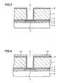
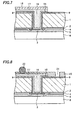
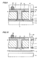
- FIGs. 1 to 10 are cross-sectional views of device intermediates during the manufacturing process of the first embodiment, shown in manufacturing order.
- a semiconductor substrate 1 formed with an electronic device e.g. a light receiving element such as CCD or an infrared ray sensor or a light emissive element (not shown) on its front surface is prepared.
- the semiconductor substrate 1 is about 300 to 700 ⁇ m in thickness, for example.
- a first insulation film 2 e.g. a silicon oxide film or a BPSG film formed by a thermal oxidation method or a CVD method
- a first insulation film 2 is formed on the front surface of the semiconductor substrate 1 to have a thickness of, for example, 2 ⁇ m.
- a metal layer made of aluminum (Al), copper (Cu), or the like is formed by a sputtering method, a plating method, or the other deposition method, and then the metal layer is etched using a resist layer (not shown) as a mask to form a pad electrode 3 having a thickness of, for example, 1 ⁇ m on the first insulation film 2.
- the pad electrode 3 is electrically connected to the electronic device or the surrounding elements on the semiconductor substrate 1.
- a passivation film 4 (e.g. a silicon nitride film formed by a CVD method) is formed on the front surface of the semiconductor substrate 1, covering a portion of the pad electrode 3.
- the first insulation film 2 and the passivation film 4 may not be formed on boundaries of individual semiconductor dies or may be formed on the boundaries for using these films as stopper layers as described below.
- a supporting body 6 is attached on the front surface of the semiconductor substrate 1 including on the pad electrode 3 with an adhesive layer 5 made of epoxy resin, a resist, acrylic, or the like interposed therebetween.
- a film-type protection tape may be used as the supporting body 6, for example, but a rigid substrate made of glass, quartz, ceramic, plastic, metal, resin, or the like is preferable for firmly supporting the thinned semiconductor substrate 1 and automating the movement of the substrate 1 without a manual control. It is not necessary to form a path (a penetrating hole or a groove) for supplying a solvent for the adhesive layer 5 in the supporting body 6.
- the supporting body 6 has a function of supporting the semiconductor substrate 1 and protecting the front surface thereof.
- back-grinding is performed to a back surface of the semiconductor substrate 1 with a back surface grinder to thin the semiconductor substrate 1 to a predetermined thickness (e.g. about 50 to 20 ⁇ m).
- This grinding process may be performed by etching or both with the grinder and by etching. There is also a case where the grinding process is not necessary depending on applications or specifications of an end-product and the initial thickness of the prepared semiconductor substrate 1.
- a resist layer 7 is selectively formed on the back surface of the semiconductor substrate 1.
- the resist layer 7 has an opening in a position corresponding to the pad electrode 3 on the back surface of the semiconductor substrate 1.
- the semiconductor substrate 1 is etched using this resist layer 7 as a mask.
- a via hole 8 is formed penetrating the semiconductor substrate 1 from its back surface to its front surface in a position corresponding to the pad electrode 3.
- the first insulation film 2 is exposed at a bottom of the via hole 8.
- etching is further performed using the resist layer 7 as a mask to remove the exposed first insulation film 2. This process of etching the first insulation film 2 may not be performed at this time, and may be performed in the other etching process simultaneously.
- the via hole 8 may not penetrate the semiconductor substrate 1 from its back surface to its front surface, and the bottom of the via hole 8 may be formed in the semiconductor substrate 1 instead.
- a second insulation film 9 e.g. a silicon oxide film or a silicon nitride film formed by a CVD method
- a second insulation film 9 is formed on the whole back surface of the semiconductor substrate 1 including in the via hole 8 as shown in Fig. 3.
- a resist layer 10 is formed on the second insulation film 9.
- the second insulation film 9 at the bottom of the via hole 8 is removed by etching using the resist layer 10 as a mask. This etching may be performed without the mask by utilizing the tendency that the second insulation film 9 is formed thicker on the back surface of the semiconductor substrate 1 and thinning toward the sidewall and the bottom of the via hole 8. Etching without the mask streamlines the manufacturing process.
- a barrier layer 15 is formed on the second insulation film 9 on the back surface of the semiconductor substrate 1 including in the via hole 8.
- a seed layer (not shown) is further formed on the barrier layer 15.
- the barrier layer 15 is made of, for example, a titanium (Ti) layer, a titanium nitride (TiN) layer, a tantalum nitride (TaN) layer, or the like.
- the seed layer is to be an electrode for forming a penetrating electrode 16 and a wiring layer 17 by a plating method that will be described below and made of, for example, metal such as copper (Cu). These layers are formed by a sputtering method, a plating method, or the other deposition method.
- a penetrating electrode 16 and the wiring layer 17 connecting with the electrode 16, that are made of copper (Cu), are formed on the barrier layer 15 and the seed layer (not shown) including in the via hole 8 by, for example, an electrolytic plating method.
- the penetrating electrode 16 and the wiring layer 17 are electrically connected to the pad electrode 3 exposed at the bottom of the via hole 8 through the barrier layer 15 and the seed layer (not shown).
- the via hole 8 may not be filled with the penetrating electrode 16 completely but partially as shown in Fig. 14. Compared with the case where the hole 8 is filled completely, this structure saves a conductive material necessary for forming the penetrating electrode 16 and the wiring layer 17 and shortens the time for forming the penetrating electrode 16 and the wiring layer 17, thereby having an advantage of increasing a throughput.
- a resist layer 18 for forming a wiring pattern is selectively formed on the wiring layer 17 on the back surface of the semiconductor substrate 1. Then, an unnecessary part of the wiring layer 17 and the seed layer is removed by etching using the resist layer 18 as a mask. By this etching, the wiring layer 17 forms a predetermined wiring pattern. Then, the barrier layer 15 formed on the back surface of the semiconductor substrate 1 is selectively removed by etching using the wiring layer 17 as a mask.
- the process of forming the barrier layer 15, the penetrating electrode 16, and the wiring layer 17 is not limited to the above process.
- a resist layer or the like is formed on the back surface of the semiconductor substrate 1 except in a region where the barrier layer 15, the wiring layer 17 and so on are to be formed, and then these barrier layer 15, wiring layer 17 and so on are formed in a region not covered with this resist layer or the like, thereby completing the patterning of the layers. This process does not need the resist layer 18.
- a protection layer 20 made of, for example, an organic material such as a solder resist or an inorganic material such as a silicon nitride film is selectively formed on the back surface of the semiconductor substrate 1 so as to have an opening 21 in a position corresponding to each of boundaries of individual semiconductor dies.
- the opening 21 may be formed in the other position, forming the opening 21 in a position corresponding to each of the boundaries of the individual semiconductor dies has a merit that the solvent supply path is formed and the semiconductor dies are separated at the same time.
- This opening 21 may not be formed at this time, and may be formed in an etching process using a resist layer 23 as a mask that will be described below.
- an opening is formed in the protection layer 20 in a conductive terminal formation region, an electrode connection layer (not shown) made of nickel and gold is formed on the wiring layer 17 exposed in the opening, and a ball-shaped conductive terminal 22 is formed thereon by screen-printing solder and reflowing the solder by heat treatment.
- the conductive terminal 22 may be formed by a dispensing method (a coating method) where solder, a ball shaped terminal or the like is coated with a dispenser, an electrolytic plating method, or the like.
- the semiconductor substrate 1 is partially removed to expose a portion of the adhesive layer 5.
- the resist layer 23 is formed on the back surface of the semiconductor substrate 1, and the second insulation film 9, the semiconductor substrate 1, the first insulation film 2, and the passivation film 4 are removed by etching using this resist layer 23 as a mask in this order.
- these layers may be etched using the protection layer 20 provided with the opening 21 as a mask, instead of using the resist layer 23 as a mask. By this etching, a portion of the adhesive layer 5 is exposed in the opening 21.
- the resist layer 23 is removed.
- the adhesive layer 5 is also removed at the same time depending on the relation between the materials of the resist layer 23 and the adhesive layer 5.
- the following process may be used for preventing the adhesive layer 5 from being removed at the time when the resist layer 23 is removed.
- the resist layer 23 is removed using the first insulation film 2 or the passivation film 4 as a stopper layer protecting the adhesive layer 5.
- the first insulation film 2 and the passivation film 4 are removed by, for example, a wet etching method or the like to expose a portion of the adhesive layer 5.
- the opening 21 is formed on each of the boundaries of the individual semiconductor dies, a number of semiconductor devices are separated in the individual semiconductor dies at the time when the adhesive layer 5 is partially exposed.
- This process does not need a dicing tape, a dicing blade, a laser, or the like that is necessary for a dicing process for separating the semiconductor devices in individual dies, thereby simplifying the manufacturing process and reducing the manufacturing cost.
- a dicing blade or a laser may be used for separating the semiconductor devices in individual semiconductor dies although etching is more preferable. Separating the semiconductor devices in individual dies with a dicing blade or a laser has a merit that a photolithography for forming the resist layer 23 is not necessary.
- a solvent 25 e.g. alcohol or acetone
- the supporting body 6 may be collected and recycled.
- This manner of removing the supporting body 6 by directly supplying the solvent 25 to the adhesive layer 5 reduces a load when the supporting body 6 is removed, thereby reducing a mechanical defect in the semiconductor device.
- the chip size package type semiconductor device having the wiring from the pad electrode 3 formed on the front surface of the semiconductor substrate 1 to the conductive terminal 22 provided on the back surface thereof is thus completed by the above described process.
- the device is electrically connected to an external circuit by mounting the conductive terminal 22 on a wiring pattern on a circuit board
- an electrode connection layer 30 made of nickel (Ni) and gold (Au) or the like is formed on the pad electrode 3 with the element such as the electronic device formed on the back surface of the semiconductor substrate 1 being protected with a protection tape or the like. Then, as shown in Fig. 11, the pad electrode 3 of one semiconductor device and the conductive terminal 22 of the other semiconductor device are connected to each other with the electrode connection layer 30 interposed therebetween.
- the electrode connection layer 30 is necessary for a reason that the pad electrode 3 made of aluminum or the like and the conductive terminal 22 made of solder or the like are hardly attached to each other or for a reason that the layer 30 prevents a material of the conductive terminal 22 flowing toward the pad electrode 3 when the devices are laminated. It is noted that Fig. 11 shows a structure where the wiring layer 17 is not extended on the back surface of the semiconductor substrate 1.
- the electrode connection layer 30 that is necessary for lamination is formed after the semiconductor device is completed, as described above.
- the semiconductor substrate 1 is already thinned, there is a problem that a mechanical defect easily occurs when the device is moved by handling it or the like.
- the electrode connection layer 30 is formed only on the pad electrode 3 on the front surface of the semiconductor substrate 1, the other part of the front surface needs to be protected when the electrode connection layer 30 is formed. Therefore, the manufacturing process becomes complex and the manufacturing cost increases.
- a manufacturing process further suitable for manufacturing the semiconductor device for the lamination is employed in addition to the manufacturing process of the first embodiment. Description thereof will be given hereinafter. The same numerals are given to the same components as those of the first embodiment, and description thereof will be simplified or omitted.
- the semiconductor substrate 1 formed with an electronic device (not shown) on its front surface is prepared.
- the first insulation film 2 is formed on the front surface of the semiconductor substrate 1.
- a metal layer made of aluminum (Al), copper (Cu), or the like is formed by a sputtering method, a plating method, or the other deposition method, and then the metal layer is etched using a resist layer (not shown) as a mask, thereby forming the pad electrode 3 on the first insulation film 2.
- the pad electrode 3 is electrically connected to the electronic device or the surrounding elements on the semiconductor substrate 1.
- the passivation film 4 is formed on the front surface of the semiconductor substrate 1, covering a portion of the pad electrode 3.
- An insulation film made of an organic resin such as polyimide may be further formed as a protection film on the passivation film 4 in order to prevent corrosion or the like.
- the electrode connection layer 30 is formed on the pad electrode 3.
- the electrode connection layer 30 is a lamination layer of a nickel (Ni) layer 31 and a gold (Au) layer 32 laminated in this order, for example, and formed by an lift-off method where these metals are sputtered in this order using a resist layer as a mask and then the resist layer is removed, or a plating method.
- the material of the electrode connection layer 30 may be changed according to needs depending on the material of the conductive terminal 22.
- the electrode connection layer 30 may be made of a titanium (Ti) layer, a copper (Cu) layer, a tin (Sn) layer, a nickel vanadium (NiV) layer, a tantalum (Ta) layer, a palladium (Pd) layer, or the like, instead of the nickel layer 31 and the gold layer 32.
- the material of the electrode connection layer 30 is not particularly limited and the layer 30 may be a single layer, a lamination layer of the above layers, or a layer made of an alloy of the above metals as long as it has a function of keeping electrical connection between the pad electrode 3 and the conductive terminal 22 and a function of protecting the pad electrode 3.
- a nickel layer/a gold layer, a titanium layer/a nickel layer/a copper layer, a titanium layer/a nickel layer/a gold layer, a titanium layer/a nickel vanadium layer/a copper layer, or the like are the examples of the lamination structure of the electrode connection layer 30.
- the supporting body 6 is attached on the front surface of the semiconductor substrate 1 with the adhesive layer 5 made of epoxy resin or the like interposed therebetween. Since subsequent processes are the same as the above described processes of the first embodiment, description thereof will be omitted.
- the second embodiment of the invention mainly has the following effect in addition to the effect obtained in the first embodiment. Since the electrode connection layer 30 is formed before the supporting body 6 is attached and the semiconductor substrate 1 is thinned, the movement of the substrate by handling it or the like is easy in the process of forming the electrode connection layer 30 and thus a mechanical defect is prevented.
- the electrode connection layer 30 is formed before the wiring layer 17, the conductive terminal 22 and so on are formed on the back surface of the semiconductor substrate 1, the special protection of the back surface of the semiconductor substrate 1 is not needed, thereby simplifying the manufacturing process. Furthermore, since the lamination structure is formed at the time when the semiconductor device is completed, the workability and efficiency are enhanced. Furthermore, when the penetrating electrode 16 is formed, the electrode connection layer 30 functions as a member reinforcing the pad electrode 3 from the front surface side of the semiconductor substrate 1. This has an advantage of preventing problems such as missing, breaking, warping, or the like of the pad electrode 3 when the penetrating electrode 16 is formed.
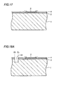
- the semiconductor substrate 1 formed with an electronic device (not shown) on its front surface is prepared. Then, the first insulation film 2, the pad electrode 3, and the passivation film 4 are formed on the front surface of the semiconductor substrate 1 in this order.
- a portion of the front surface of the semiconductor substrate 1 is removed to form a groove 40.
- the groove 40 is to form a part of a solvent supply path that will be described below, and its depth is preferably about 10 ⁇ m or more.
- the groove 40 is preferably provided along the dicing line DL as shown in Fig. 18A.
- the process of forming the solvent supply path and the process of separating the semiconductor dies are performed at the same time as described below.
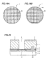
- Figs. 19A and 19B are plan views of the semiconductor substrate 1 formed with the groove 40.
- the groove 40 is formed by the so-called half-etching.
- the groove 40 as shown in Fig. 18A is formed by removing a portion of the semiconductor substrate 1 by etching using a resist layer (not shown) as a mask.
- a groove 40a as shown in Fig. 18B may be formed by mechanically removing a portion of the semiconductor substrate 1 with a dicing blade. With the dicing blade, the cross-section of the groove 40a forms the shape of the blade as shown in Fig. 18B (the width on the front surface side of the semiconductor substrate 1 is slightly larger than on the other side). The formation of such a groove of which the width is larger on the front surface side of the semiconductor substrate 1 is preferable for smoothly supplying the solvent when the supporting body is removed.
- the cross-section of the groove may form such a shape that the width increases toward the front surface side of the semiconductor substrate 1 and a convex is formed on the back surface side (a groove 40b) as shown in Fig. 18C by combining isotropic etching and anisotropic etching for forming the groove.
- a corrosive substance e.g. chemicals in the wet process
- a resist layer is formed so as to avoid the remove of the periphery 41, and the substrate 1 is etched using this resist layer as a mask to form the desired groove 40 except on the periphery 41.
- the supporting body 6 is attached on the front surface of the semiconductor substrate 1 with the adhesive layer 5 interposed therebetween. Then, back-grinding is performed to the back surface of the semiconductor substrate 1 with a back surface grinder to thin the semiconductor substrate 1 to a predetermined thickness. Then, the resist layer 7 is selectively formed on the back surface of the semiconductor substrate 1. Then, the semiconductor substrate 1 is etched using the resist layer 7 as a mask to form the via hole 8.
- the second insulation film 9 the barrier layer 15, the seed layer, the penetrating electrode 16, the wiring layer 17, the protection layer 20, and the conductive terminal 22 are formed.
- the process of forming these is the same as that of the first embodiment.
- a portion of the semiconductor substrate 1 is removed along the predetermined dicing line DL to form an opening 41 (the solvent supply path) exposing a portion of the adhesive layer 5.
- the opening 41 is connected to the groove 40 at its bottom.
- the protection layer 20, the second insulation film 9, and the semiconductor substrate 1 are removed in this order with a dicing blade, for example, until the opening reaches the groove 40.
- a dicing blade since it is not necessary to insert the dicing blade deep into the semiconductor substrate 1 by an amount of a height X of the groove 40 in a vertical direction, there is significantly reduced possibility that the dicing blade contacts and damages the supporting body 6 when the opening 41 is formed.
- the method of forming the opening 41 is not limited to this.
- a resist layer (not shown) may be formed on the back surface of the semiconductor substrate 1, and the opening 41 may be formed by removing the protection layer 20, the second insulation film 9, and the semiconductor substrate 1 by etching using the resist layer as a mask in this order.
- the opening 41 may be formed by providing an opening in the protection layer 20 in a position corresponding to the groove 40 and performing etching using the protection layer 20 as a mask.
- the opening 41 may be formed with a laser.
- the opening 41 is formed by etching, there is an advantage that the cut surface is formed smooth and cracking or chipping is prevented since the sidewall (the section) of the opening does not suffer mechanical stress and much damage, compared with the formation with a dicing blade.
- the formation of the groove 40 and the opening 41 along the dicing line DL enables simultaneous performance of these processes, thereby simplifying the manufacturing process and reducing the manufacturing cost.
- the solvent 25 is supplied to the exposed adhesive layer 5 through the opening 41 to gradually reduce its adhesion, and thereby the supporting body 6 is removed from the semiconductor substrate 1.
- the supporting body 6 since the supporting body 6 is not damaged during the formation of the opening 41 as described above, the supporting body 6 is collected and effectively recycled.
- the chip size package type semiconductor device having a wiring from the pad electrode 3 formed on the front surface of the semiconductor substrate 1 to the conductive terminal 22 on the back surface thereof is completed.
- the manufacturing process is simplified and the cost is reduced. Furthermore, this prevents the influence of the solvent supply path such as outgassing or infiltration of a corrosive substance.
- the supporting body is not damaged even when the semiconductor dies are separated with a dicing blade. This facilitates the recycle of the supporting body and reduces the manufacturing cost.
- the semiconductor device may be manufactured by removing the supporting body as described below. As shown in Fig. 24, a portion of the front surface of the semiconductor substrate 1 is removed, and half-etched along the dicing line DL to provide a groove 50.
- the depth of the groove 50 equals the desired thickness of the semiconductor substrate 1, i.e., the thickness of the semiconductor substrate 1 after back-ground, for example, about 50 ⁇ m.
- the supporting body 6 is attached on the front surface of the semiconductor substrate 1 with the adhesive layer 5 interposed therebetween.
- back-grinding is performed to the back surface of the semiconductor substrate 1 with a back surface grinder to thin the semiconductor substrate 1 to a predetermined thickness (e.g. about 50 ⁇ m).
- the adhesive layer 5 is exposed from the groove 50 by this back-grinding.
- Subsequent processes are almost the same as those described above, where the via hole, the wiring layer and so on are formed, the adhesive layer 5 in the groove 50 is exposed, the solvent is supplied from the-portion exposing the layer 5, the supporting body 6 is removed, and thereby individual semiconductor devices are completed.
- the feature of this process is that the thickness of the groove 50 equals the thickness of the substrate after background, and a portion of the adhesive layer 5 is simultaneously exposed by the back-grinding.
- the remove of the semiconductor substrate 1 for securing the solvent supply path is simultaneously performed by the back-grinding, the subsequent process of removing a portion of the semiconductor substrate 1 with a dicing blade or etching is not necessary, and the supporting body 6 is not damaged.
- the process shown in the second embodiment may be added (the process of forming the electrode connect layer 30).
- the invention is also applied to an LGA (land grid array) type, a CSP, and a flip chip type semiconductor devices having no ball-shaped conductive terminal.
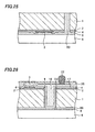
- the semiconductor device is attached on the front surface side (the side formed with the element) of the semiconductor substrate 1 in the above described embodiments, it is possible to form the semiconductor device with the supporting body 6 being attached on the other side (the surface not formed with the element) as shown in Fig. 26.
- an opening (not shown) exposing a portion of the adhesive layer 5 is formed from the front surface side of the semiconductor substrate 1 by the same process as in the above described embodiments.
- a solvent is supplied in the opening to gradually reduce the adhesion of the adhesive layer 5, and thereby the supporting body 6 is removed from the semiconductor substrate 1.
- This semiconductor device has the pad electrode 3, the wiring layer 17, the conductive terminal 22 and so on the front surface side (the surface formed with the element) of the semiconductor substrate 1.
- the device is electrically connected to an external circuit by mounting the conductive terminal 22 on a wiring pattern on a circuit board.
- the following process may be employed after the supporting body 6 of the semiconductor device shown in Fig. 26 is removed.
- the insulation film 60 formed on the back surface of the semiconductor substrate 1 in a position corresponding to the penetrating electrode 16 e.g. a silicon oxide film formed by a CVD method
- an electrode connection layer e.g. a lamination layer of a nickel layer and a gold layer
- the penetrating electrode 16 and the electrode of the other semiconductor device are connected through the electrode connection layer, thereby completing the lamination of the semiconductor devices.
- the barrier layer 15 in the opening is removed to expose the penetrating electrode 16 from the back surface side of the semiconductor substrate 1.
- an electrode connection layer (not shown) (e.g. a lamination layer of a nickel layer and a gold layer) is formed on the exposed surface of the penetrating electrode 16 by, for example, a plating method, and the penetrating electrode 16 and the electrode of the other semiconductor device are connected through the electrode connection layer, thereby completing the lamination of the semiconductor devices.
- the same numerals are given to the same components as those described above, and description thereof is omitted.
- the supporting body 6 is attached on any surface of the semiconductor substrate.
- the invention is broadly applied to the method of manufacturing the semiconductor device with the supporting body.
- the embodiments of the invention do not require the supporting body formed with the solvent supply path such as a penetrating hole or a groove. Therefore, the manufacturing process is simplified, the manufacturing cost is reduced, and bad influences such as outgassing or infiltration of a corrosive substance due to the solvent supply path is prevented.
- the electrode connection layer on the pad electrode for connection to the electrode of the other semiconductor device before the supporting body is attached enables the manufacturing of a high-performance semiconductor device for lamination having high reliability and increases the yield thereof. Furthermore, the lamination of the semiconductor die is performed after the individual semiconductor dies are separated, thereby enhancing the workability.
Landscapes
- Internal Circuitry In Semiconductor Integrated Circuit Devices (AREA)
- Weting (AREA)
- Mechanical Treatment Of Semiconductor (AREA)
Abstract
Description
- The invention relates to a method of manufacturing a semiconductor device, particularly, a method of manufacturing a semiconductor device with a supporting body.
- In recent years, thinner and smaller semiconductor dies have been required for increasing the packaging density. For satisfying this, it is necessary to thin a semiconductor substrate made of silicon or the like. However, the thin substrate can not be moved in a manufacturing process since it warps or breaks due to its low strength. Therefore, generally, a supporting body such as a glass substrate or a protection tape is attached on one surface of the semiconductor substrate, and the other surface where the supporting body is not attached is thinned by grinding it with a grinder or the like.
- Figs. 15 and 16 are schematic cross-sectional views showing a process of removing a supporting body in a conventional method of manufacturing a semiconductor device. As shown in Fig. 15, a
pad electrode 101 made of aluminum or the like is formed on a front surface of asemiconductor substrate 100 made of silicon or the like with afirst insulation film 102 such as a silicon oxide film interposed therebetween. Apassivation film 103 such as a silicon nitride film covers a portion of thepad electrode 101. Aglass substrate 104 as a supporting body is further attached on the front surface of thesemiconductor substrate 100 with anadhesive layer 105 interposed therebetween. A plurality of penetratingholes 106 for supplying a solvent for theadhesive layer 105 is formed in theglass substrate 104. A film-type protection tape may be used as the supporting body instead of theglass substrate 104 or a rigid substrate made of metal, resin, or the like. - A
via hole 107 is formed penetrating thesemiconductor substrate 100 from its back surface to thepad electrode 101. Asecond insulation film 108 such as a silicon oxide film is formed on a sidewall of this viahole 107 and the back surface of thesemiconductor substrate 100. - Furthermore, a
barrier layer 109 and apenetrating electrode 110 electrically connected to thepad electrode 101 are formed in thevia hole 107, and awiring layer 111 connecting with the penetratingelectrode 110 is extended on the back surface of thesemiconductor substrate 100. Aprotection layer 112 made of a solder resist or the like is formed covering thesecond insulation film 108, thewiring layer 111, and thepenetrating electrode 110, an opening is formed in a predetermined region of theprotection layer 112, and a ball-shapedconductive terminal 113 is formed in this opening. - Then, as shown in Fig. 16, a
dicing tape 115 is attached on the back surface of thesemiconductor substrate 100, and a solvent (e.g. alcohol or acetone) for theadhesive layer 105 is supplied from the penetratingholes 106 to remove theglass substrate 104. Then, the semiconductor substrate is cut along a dicing line DL with a dicing blade or a laser and individual semiconductor dies are separated from each other. - When the film-type protection tape is used instead of the
glass substrate 104, the protection tape (supporting body) is removed after the dicing, by, for example, peeling it with an adhesive tape (see Fig. 7 etc. in theJapanese Patent Application Publication No. 2002-270676 - The relevant technologies are disclosed in
Japanese Patent Application Publication Nos. 2005-191550 2002-270676 2001-185519 - However, in the conventional method of manufacturing the semiconductor device described above, since the fine penetrating
holes 106 or grooves as paths for supplying the solvent for theadhesive layer 105 are formed in theglass substrate 104 as the supporting body, there is a problem that the manufacturing process is complex and the cost is high. Using such a supporting body formed with the solvent supply paths also causes undesired influence on the process of manufacturing the semiconductor device, such as outgassing or infiltration of a corrosive substance at the paths. Furthermore, the strength of the supporting body lowers by forming the solvent supply paths, and the supporting body may suffer mechanical damage. Furthermore, it is difficult to check the metal contamination state of the solvent supply paths such as the penetratingholes 106 or the grooves for recycling the supporting body. - Although the film-type protection tape may be used as the supporting body instead of the rigid supporting body made of glass, quartz, ceramic, metal, resin, or the like formed with the solvent supply paths such as the penetrating
holes 106 or the grooves, the conventional method of removing the protection tape has a problem of causing a mechanical defect in the thinned semiconductor device when the protection tape is removed. Using the protection tape as the supporting body also causes a problem that the thermal resistance of the protection tape needs to be taken into account in the manufacturing process. - Therefore, the invention is directed to simplification of the process of manufacturing the semiconductor device with the supporting body, reduction of the manufacturing cost, and enhancement of the reliability and yield of the semiconductor device. The invention is also directed to realization of the method of manufacturing the semiconductor device suitable for thinning and miniaturizing the semiconductor device.
- The solution according to the invention resides in the features of the independent claims and preferably in those of the dependent claims. The invention provides a method of manufacturing a semiconductor device including: providing a semiconductor substrate formed with a pad electrode on its front surface; attaching a supporting body on the front surface of the semiconductor substrate with an adhesive layer interposed therebetween; forming a via hole in the semiconductor substrate; forming a penetrating electrode electrically connected to the pad electrode in the via hole; forming a protection layer covering a back surface of the semiconductor substrate including the penetrating electrode; removing a portion of the semiconductor substrate to expose a portion of the adhesive layer; and separating the supporting body from the semiconductor substrate by supplying a solvent dissolving the adhesive layer from a portion exposing the adhesive layer.
- The method of the invention preferably includes forming an electrode connection layer for connection to an electrode of another semiconductor device on the pad electrode before attaching the supporting body.
- In the method of the invention, a path for supplying the solvent is preferably not formed in the supporting body.
- The invention also provides a method of manufacturing a semiconductor device including: attaching a supporting body on a front surface of a semiconductor substrate with an adhesive layer interposed therebetween; removing a portion of the semiconductor substrate to form an opening exposing the adhesive layer from a back surface of the semiconductor substrate; and separating the supporting body from the semiconductor substrate by supplying a solvent dissolving the adhesive layer from a portion exposing the adhesive layer.
- The invention also provides a method of manufacturing a semiconductor device including: preparing a semiconductor substrate formed with a pad electrode with an insulation film interposed therebetween; attaching a supporting body on a front surface of the semiconductor substrate with an adhesive layer interposed therebetween; exposing the pad electrode by removing the semiconductor substrate and the insulation film; forming a wiring layer electrically connected to the exposed pad electrode; forming a protection film covering a back surface of the semiconductor substrate including the wiring layer; removing a portion of the semiconductor substrate to expose a portion of the adhesive layer; and separating the supporting body from the semiconductor substrate by supplying a solvent dissolving the adhesive layer from a portion exposing the adhesive layer.
-
- Figs. 1 to 11 and 14 are cross-sectional views for explaining a method of manufacturing a semiconductor device of a first embodiment of the invention.
- Figs. 12 and 13 are cross-sectional views for explaining a method of manufacturing a semiconductor device of a second embodiment of the invention.
- Figs. 15 and 16 are cross-sectional views for explaining a conventional method of manufacturing a semiconductor device.
- Figs. 17 to 18C and 20 to 25 are cross-sectional views for explaining a method of manufacturing a semiconductor device of a third embodiment of the invention.
- Figs. 19A and 19B are plan views for explaining the method of manufacturing the semiconductor device of the third embodiment of the invention.
- Fig. 26 is a cross-sectional view for explaining an example of modifications of the semiconductor device of the embodiments of the invention.
- A first embodiment of the invention will be described referring to figures. Figs. 1 to 10 are cross-sectional views of device intermediates during the manufacturing process of the first embodiment, shown in manufacturing order.
- First, as shown in Fig. 1, a
semiconductor substrate 1 formed with an electronic device (e.g. a light receiving element such as CCD or an infrared ray sensor or a light emissive element) (not shown) on its front surface is prepared. Thesemiconductor substrate 1 is about 300 to 700µm in thickness, for example. Then, a first insulation film 2 (e.g. a silicon oxide film or a BPSG film formed by a thermal oxidation method or a CVD method) is formed on the front surface of thesemiconductor substrate 1 to have a thickness of, for example, 2µm. - Then, a metal layer made of aluminum (Al), copper (Cu), or the like is formed by a sputtering method, a plating method, or the other deposition method, and then the metal layer is etched using a resist layer (not shown) as a mask to form a
pad electrode 3 having a thickness of, for example, 1µm on thefirst insulation film 2. Thepad electrode 3 is electrically connected to the electronic device or the surrounding elements on thesemiconductor substrate 1. - Then, a passivation film 4 (e.g. a silicon nitride film formed by a CVD method) is formed on the front surface of the
semiconductor substrate 1, covering a portion of thepad electrode 3. Thefirst insulation film 2 and thepassivation film 4 may not be formed on boundaries of individual semiconductor dies or may be formed on the boundaries for using these films as stopper layers as described below. - Then, a supporting
body 6 is attached on the front surface of thesemiconductor substrate 1 including on thepad electrode 3 with anadhesive layer 5 made of epoxy resin, a resist, acrylic, or the like interposed therebetween. A film-type protection tape may be used as the supportingbody 6, for example, but a rigid substrate made of glass, quartz, ceramic, plastic, metal, resin, or the like is preferable for firmly supporting thethinned semiconductor substrate 1 and automating the movement of thesubstrate 1 without a manual control. It is not necessary to form a path (a penetrating hole or a groove) for supplying a solvent for theadhesive layer 5 in the supportingbody 6. The supportingbody 6 has a function of supporting thesemiconductor substrate 1 and protecting the front surface thereof. - Then, back-grinding is performed to a back surface of the
semiconductor substrate 1 with a back surface grinder to thin thesemiconductor substrate 1 to a predetermined thickness (e.g. about 50 to 20µm). This grinding process may be performed by etching or both with the grinder and by etching. There is also a case where the grinding process is not necessary depending on applications or specifications of an end-product and the initial thickness of the preparedsemiconductor substrate 1. - Then, as shown in Fig. 2, a
resist layer 7 is selectively formed on the back surface of thesemiconductor substrate 1. Theresist layer 7 has an opening in a position corresponding to thepad electrode 3 on the back surface of thesemiconductor substrate 1. Then, thesemiconductor substrate 1 is etched using thisresist layer 7 as a mask. By this etching, avia hole 8 is formed penetrating thesemiconductor substrate 1 from its back surface to its front surface in a position corresponding to thepad electrode 3. Thefirst insulation film 2 is exposed at a bottom of the viahole 8. Then, etching is further performed using the resistlayer 7 as a mask to remove the exposedfirst insulation film 2. This process of etching thefirst insulation film 2 may not be performed at this time, and may be performed in the other etching process simultaneously. - Although not shown, the via
hole 8 may not penetrate thesemiconductor substrate 1 from its back surface to its front surface, and the bottom of the viahole 8 may be formed in thesemiconductor substrate 1 instead. - Then, the resist
layer 7 is removed, and a second insulation film 9 (e.g. a silicon oxide film or a silicon nitride film formed by a CVD method) is formed on the whole back surface of thesemiconductor substrate 1 including in the viahole 8 as shown in Fig. 3. - Then, as shown in Fig. 4, a resist
layer 10 is formed on thesecond insulation film 9. Then, as shown in Fig. 5, thesecond insulation film 9 at the bottom of the viahole 8 is removed by etching using the resistlayer 10 as a mask. This etching may be performed without the mask by utilizing the tendency that thesecond insulation film 9 is formed thicker on the back surface of thesemiconductor substrate 1 and thinning toward the sidewall and the bottom of the viahole 8. Etching without the mask streamlines the manufacturing process. - Then, as shown in Fig. 6, a
barrier layer 15 is formed on thesecond insulation film 9 on the back surface of thesemiconductor substrate 1 including in the viahole 8. A seed layer (not shown) is further formed on thebarrier layer 15. Thebarrier layer 15 is made of, for example, a titanium (Ti) layer, a titanium nitride (TiN) layer, a tantalum nitride (TaN) layer, or the like. The seed layer is to be an electrode for forming a penetratingelectrode 16 and awiring layer 17 by a plating method that will be described below and made of, for example, metal such as copper (Cu). These layers are formed by a sputtering method, a plating method, or the other deposition method. - Then, a penetrating
electrode 16 and thewiring layer 17 connecting with theelectrode 16, that are made of copper (Cu), are formed on thebarrier layer 15 and the seed layer (not shown) including in the viahole 8 by, for example, an electrolytic plating method. The penetratingelectrode 16 and thewiring layer 17 are electrically connected to thepad electrode 3 exposed at the bottom of the viahole 8 through thebarrier layer 15 and the seed layer (not shown). - The via
hole 8 may not be filled with the penetratingelectrode 16 completely but partially as shown in Fig. 14. Compared with the case where thehole 8 is filled completely, this structure saves a conductive material necessary for forming the penetratingelectrode 16 and thewiring layer 17 and shortens the time for forming the penetratingelectrode 16 and thewiring layer 17, thereby having an advantage of increasing a throughput. - Then, as shown in Fig. 7, a resist
layer 18 for forming a wiring pattern is selectively formed on thewiring layer 17 on the back surface of thesemiconductor substrate 1. Then, an unnecessary part of thewiring layer 17 and the seed layer is removed by etching using the resistlayer 18 as a mask. By this etching, thewiring layer 17 forms a predetermined wiring pattern. Then, thebarrier layer 15 formed on the back surface of thesemiconductor substrate 1 is selectively removed by etching using thewiring layer 17 as a mask. - The process of forming the
barrier layer 15, the penetratingelectrode 16, and thewiring layer 17 is not limited to the above process. For example, a resist layer or the like is formed on the back surface of thesemiconductor substrate 1 except in a region where thebarrier layer 15, thewiring layer 17 and so on are to be formed, and then thesebarrier layer 15,wiring layer 17 and so on are formed in a region not covered with this resist layer or the like, thereby completing the patterning of the layers. This process does not need the resistlayer 18. - Then, as shown in Fig. 8, a
protection layer 20 made of, for example, an organic material such as a solder resist or an inorganic material such as a silicon nitride film is selectively formed on the back surface of thesemiconductor substrate 1 so as to have anopening 21 in a position corresponding to each of boundaries of individual semiconductor dies. Although theopening 21 may be formed in the other position, forming theopening 21 in a position corresponding to each of the boundaries of the individual semiconductor dies has a merit that the solvent supply path is formed and the semiconductor dies are separated at the same time. Thisopening 21 may not be formed at this time, and may be formed in an etching process using a resistlayer 23 as a mask that will be described below. Furthermore, an opening is formed in theprotection layer 20 in a conductive terminal formation region, an electrode connection layer (not shown) made of nickel and gold is formed on thewiring layer 17 exposed in the opening, and a ball-shapedconductive terminal 22 is formed thereon by screen-printing solder and reflowing the solder by heat treatment. Theconductive terminal 22 may be formed by a dispensing method (a coating method) where solder, a ball shaped terminal or the like is coated with a dispenser, an electrolytic plating method, or the like. - Then, as shown in Fig. 9, the
semiconductor substrate 1 is partially removed to expose a portion of theadhesive layer 5. In detail, for example, the resistlayer 23 is formed on the back surface of thesemiconductor substrate 1, and thesecond insulation film 9, thesemiconductor substrate 1, thefirst insulation film 2, and thepassivation film 4 are removed by etching using this resistlayer 23 as a mask in this order. Alternatively, these layers may be etched using theprotection layer 20 provided with theopening 21 as a mask, instead of using the resistlayer 23 as a mask. By this etching, a portion of theadhesive layer 5 is exposed in theopening 21. - Then, the resist
layer 23 is removed. At this time, when theadhesive layer 5 is exposed, there may be a case where theadhesive layer 5 is also removed at the same time depending on the relation between the materials of the resistlayer 23 and theadhesive layer 5. The following process may be used for preventing theadhesive layer 5 from being removed at the time when the resistlayer 23 is removed. First, when thesecond insulation film 9 and thesemiconductor substrate 1 are etched using the resistlayer 23 as a mask, thepassivation film 4 or thefirst insulation film 2 is left as it is without being etched. Then, the resistlayer 23 is removed using thefirst insulation film 2 or thepassivation film 4 as a stopper layer protecting theadhesive layer 5. Then, thefirst insulation film 2 and thepassivation film 4 are removed by, for example, a wet etching method or the like to expose a portion of theadhesive layer 5. - In the case where the
opening 21 is formed on each of the boundaries of the individual semiconductor dies, a number of semiconductor devices are separated in the individual semiconductor dies at the time when theadhesive layer 5 is partially exposed. This process does not need a dicing tape, a dicing blade, a laser, or the like that is necessary for a dicing process for separating the semiconductor devices in individual dies, thereby simplifying the manufacturing process and reducing the manufacturing cost. - Furthermore, mechanical stress is not applied to the sidewall (the section) of the opening in this embodiment, compared with the case of using a dicing blade, thereby providing advantages of formation of a smooth section without damage and prevention of cracking or chipping. This prevents a mechanical defect occurring during the dicing process, thereby realizing a semiconductor device having high reliability and increasing the yield thereof. Furthermore, there is no need to control pressure of a dicing blade, a cutting speed, or the like, thereby simplifying the manufacturing process.
- A dicing blade or a laser may be used for separating the semiconductor devices in individual semiconductor dies although etching is more preferable. Separating the semiconductor devices in individual dies with a dicing blade or a laser has a merit that a photolithography for forming the resist
layer 23 is not necessary. - Then, as shown in Fig. 10, a solvent 25 (e.g. alcohol or acetone) is supplied to the exposed
adhesive layer 5 through theopening 21 to gradually reduce its adhesion, and thereby the supportingbody 6 is removed from thesemiconductor substrate 1. The supportingbody 6 may be collected and recycled. - This manner of removing the supporting
body 6 by directly supplying the solvent 25 to theadhesive layer 5 reduces a load when the supportingbody 6 is removed, thereby reducing a mechanical defect in the semiconductor device. - The chip size package type semiconductor device having the wiring from the
pad electrode 3 formed on the front surface of thesemiconductor substrate 1 to theconductive terminal 22 provided on the back surface thereof is thus completed by the above described process. When this semiconductor device is mounted on electronic equipment, the device is electrically connected to an external circuit by mounting theconductive terminal 22 on a wiring pattern on a circuit board - When the semiconductor device completed by the above process is used for lamination with the other semiconductor device, an
electrode connection layer 30 made of nickel (Ni) and gold (Au) or the like is formed on thepad electrode 3 with the element such as the electronic device formed on the back surface of thesemiconductor substrate 1 being protected with a protection tape or the like. Then, as shown in Fig. 11, thepad electrode 3 of one semiconductor device and theconductive terminal 22 of the other semiconductor device are connected to each other with theelectrode connection layer 30 interposed therebetween. Theelectrode connection layer 30 is necessary for a reason that thepad electrode 3 made of aluminum or the like and theconductive terminal 22 made of solder or the like are hardly attached to each other or for a reason that thelayer 30 prevents a material of theconductive terminal 22 flowing toward thepad electrode 3 when the devices are laminated. It is noted that Fig. 11 shows a structure where thewiring layer 17 is not extended on the back surface of thesemiconductor substrate 1. - Next, a second embodiment of the invention will be described referring to figures. In the method of manufacturing the semiconductor device of the first embodiment, when the completed semiconductor device is used for lamination, generally, the
electrode connection layer 30 that is necessary for lamination is formed after the semiconductor device is completed, as described above. However, since thesemiconductor substrate 1 is already thinned, there is a problem that a mechanical defect easily occurs when the device is moved by handling it or the like. Furthermore, since theelectrode connection layer 30 is formed only on thepad electrode 3 on the front surface of thesemiconductor substrate 1, the other part of the front surface needs to be protected when theelectrode connection layer 30 is formed. Therefore, the manufacturing process becomes complex and the manufacturing cost increases. - In the second embodiment of the invention, a manufacturing process further suitable for manufacturing the semiconductor device for the lamination is employed in addition to the manufacturing process of the first embodiment. Description thereof will be given hereinafter. The same numerals are given to the same components as those of the first embodiment, and description thereof will be simplified or omitted.
- First, as shown in Fig. 12, the
semiconductor substrate 1 formed with an electronic device (not shown) on its front surface is prepared. Then, thefirst insulation film 2 is formed on the front surface of thesemiconductor substrate 1. Then, a metal layer made of aluminum (Al), copper (Cu), or the like is formed by a sputtering method, a plating method, or the other deposition method, and then the metal layer is etched using a resist layer (not shown) as a mask, thereby forming thepad electrode 3 on thefirst insulation film 2. Thepad electrode 3 is electrically connected to the electronic device or the surrounding elements on thesemiconductor substrate 1. Then, thepassivation film 4 is formed on the front surface of thesemiconductor substrate 1, covering a portion of thepad electrode 3. An insulation film made of an organic resin such as polyimide may be further formed as a protection film on thepassivation film 4 in order to prevent corrosion or the like. - Then, as shown in Fig. 13, the
electrode connection layer 30 is formed on thepad electrode 3. Theelectrode connection layer 30 is a lamination layer of a nickel (Ni)layer 31 and a gold (Au) layer 32 laminated in this order, for example, and formed by an lift-off method where these metals are sputtered in this order using a resist layer as a mask and then the resist layer is removed, or a plating method. The material of theelectrode connection layer 30 may be changed according to needs depending on the material of theconductive terminal 22. In detail, theelectrode connection layer 30 may be made of a titanium (Ti) layer, a copper (Cu) layer, a tin (Sn) layer, a nickel vanadium (NiV) layer, a tantalum (Ta) layer, a palladium (Pd) layer, or the like, instead of thenickel layer 31 and the gold layer 32. The material of theelectrode connection layer 30 is not particularly limited and thelayer 30 may be a single layer, a lamination layer of the above layers, or a layer made of an alloy of the above metals as long as it has a function of keeping electrical connection between thepad electrode 3 and theconductive terminal 22 and a function of protecting thepad electrode 3. A nickel layer/a gold layer, a titanium layer/a nickel layer/a copper layer, a titanium layer/a nickel layer/a gold layer, a titanium layer/a nickel vanadium layer/a copper layer, or the like are the examples of the lamination structure of theelectrode connection layer 30. - Then, the supporting
body 6 is attached on the front surface of thesemiconductor substrate 1 with theadhesive layer 5 made of epoxy resin or the like interposed therebetween. Since subsequent processes are the same as the above described processes of the first embodiment, description thereof will be omitted. - The second embodiment of the invention mainly has the following effect in addition to the effect obtained in the first embodiment. Since the
electrode connection layer 30 is formed before the supportingbody 6 is attached and thesemiconductor substrate 1 is thinned, the movement of the substrate by handling it or the like is easy in the process of forming theelectrode connection layer 30 and thus a mechanical defect is prevented. - Furthermore, since the
electrode connection layer 30 is formed before thewiring layer 17, theconductive terminal 22 and so on are formed on the back surface of thesemiconductor substrate 1, the special protection of the back surface of thesemiconductor substrate 1 is not needed, thereby simplifying the manufacturing process. Furthermore, since the lamination structure is formed at the time when the semiconductor device is completed, the workability and efficiency are enhanced. Furthermore, when the penetratingelectrode 16 is formed, theelectrode connection layer 30 functions as a member reinforcing thepad electrode 3 from the front surface side of thesemiconductor substrate 1. This has an advantage of preventing problems such as missing, breaking, warping, or the like of thepad electrode 3 when the penetratingelectrode 16 is formed. - Next, a third embodiment of the invention will be described referring to figures. The same numerals are given to the same components in the structure and the manufacturing process as those of the first or second embodiment, and description thereof will be simplified or omitted.
- First, as shown in Fig. 17, the
semiconductor substrate 1 formed with an electronic device (not shown) on its front surface is prepared. Then, thefirst insulation film 2, thepad electrode 3, and thepassivation film 4 are formed on the front surface of thesemiconductor substrate 1 in this order. - Then, as shown in Fig. 18A, a portion of the front surface of the
semiconductor substrate 1 is removed to form agroove 40. Thegroove 40 is to form a part of a solvent supply path that will be described below, and its depth is preferably about 10µm or more. - The
groove 40 is preferably provided along the dicing line DL as shown in Fig. 18A. By forming thegroove 40 along the dicing line DL, the process of forming the solvent supply path and the process of separating the semiconductor dies (the so-called dicing process) are performed at the same time as described below. Figs. 19A and 19B are plan views of thesemiconductor substrate 1 formed with thegroove 40. - The
groove 40 is formed by the so-called half-etching. In detail, for example, thegroove 40 as shown in Fig. 18A is formed by removing a portion of thesemiconductor substrate 1 by etching using a resist layer (not shown) as a mask. - Alternatively, a
groove 40a as shown in Fig. 18B may be formed by mechanically removing a portion of thesemiconductor substrate 1 with a dicing blade. With the dicing blade, the cross-section of thegroove 40a forms the shape of the blade as shown in Fig. 18B (the width on the front surface side of thesemiconductor substrate 1 is slightly larger than on the other side). The formation of such a groove of which the width is larger on the front surface side of thesemiconductor substrate 1 is preferable for smoothly supplying the solvent when the supporting body is removed. Alternatively, the cross-section of the groove may form such a shape that the width increases toward the front surface side of thesemiconductor substrate 1 and a convex is formed on the back surface side (agroove 40b) as shown in Fig. 18C by combining isotropic etching and anisotropic etching for forming the groove. - As shown in Fig. 19A, however, when the
groove 40 is exposed from the periphery of thesemiconductor substrate 1, there may be a case where a corrosive substance (e.g. chemicals in the wet process) enters thesemiconductor substrate 1 from outside (from the surroundings of thesemiconductor substrate 1 or the like) through thegrooves 40 to provide undesired influence on thesubstrate 1 after the supporting body is attached. Therefore, it is preferable to form thegroove 40 in thesemiconductor substrate 1 except on itsperiphery 41 of a predetermined width (e.g. about 3 mm), that is, so as to avoid exposing thegroove 40 to the outside when the supportingbody 6 is attached on the substrate, as shown in Fig. 19B. In detail, for example, a resist layer is formed so as to avoid the remove of theperiphery 41, and thesubstrate 1 is etched using this resist layer as a mask to form the desiredgroove 40 except on theperiphery 41. By this manufacturing process, since theperiphery 41 of thesemiconductor substrate 1 functions as a protection barrier even after the supportingbody 6 is attached on thesubstrate 1, the front surface of thesemiconductor substrate 1 is protected against infiltration of a corrosive substance. - Then, as shown in Fig. 20, the supporting
body 6 is attached on the front surface of thesemiconductor substrate 1 with theadhesive layer 5 interposed therebetween. Then, back-grinding is performed to the back surface of thesemiconductor substrate 1 with a back surface grinder to thin thesemiconductor substrate 1 to a predetermined thickness. Then, the resistlayer 7 is selectively formed on the back surface of thesemiconductor substrate 1. Then, thesemiconductor substrate 1 is etched using the resistlayer 7 as a mask to form the viahole 8. - Then, as shown in Fig. 21, the
second insulation film 9, thebarrier layer 15, the seed layer, the penetratingelectrode 16, thewiring layer 17, theprotection layer 20, and theconductive terminal 22 are formed. The process of forming these is the same as that of the first embodiment. - Then, as shown in Fig. 22, a portion of the
semiconductor substrate 1 is removed along the predetermined dicing line DL to form an opening 41 (the solvent supply path) exposing a portion of theadhesive layer 5. Theopening 41 is connected to thegroove 40 at its bottom. In detail, theprotection layer 20, thesecond insulation film 9, and thesemiconductor substrate 1 are removed in this order with a dicing blade, for example, until the opening reaches thegroove 40. In this embodiment, since it is not necessary to insert the dicing blade deep into thesemiconductor substrate 1 by an amount of a height X of thegroove 40 in a vertical direction, there is significantly reduced possibility that the dicing blade contacts and damages the supportingbody 6 when theopening 41 is formed. - The method of forming the
opening 41 is not limited to this. For example, a resist layer (not shown) may be formed on the back surface of thesemiconductor substrate 1, and theopening 41 may be formed by removing theprotection layer 20, thesecond insulation film 9, and thesemiconductor substrate 1 by etching using the resist layer as a mask in this order. Alternatively, theopening 41 may be formed by providing an opening in theprotection layer 20 in a position corresponding to thegroove 40 and performing etching using theprotection layer 20 as a mask. Alternatively, theopening 41 may be formed with a laser. - When the
opening 41 is formed by etching, there is an advantage that the cut surface is formed smooth and cracking or chipping is prevented since the sidewall (the section) of the opening does not suffer mechanical stress and much damage, compared with the formation with a dicing blade. - Although it is possible to separate the semiconductor dies by dicing in the different process after the
opening 41 is formed to expose a portion of theadhesive layer 5, it is preferable to perform these processes at the same time. That is, the formation of thegroove 40 and theopening 41 along the dicing line DL enables simultaneous performance of these processes, thereby simplifying the manufacturing process and reducing the manufacturing cost. - Then, as shown in Fig. 23, the solvent 25 is supplied to the exposed
adhesive layer 5 through theopening 41 to gradually reduce its adhesion, and thereby the supportingbody 6 is removed from thesemiconductor substrate 1. In this embodiment, since the supportingbody 6 is not damaged during the formation of theopening 41 as described above, the supportingbody 6 is collected and effectively recycled. - Furthermore, by directly supplying the solvent 25 to the
adhesive layer 5 in this manner to remove the supportingbody 6, a load when the supportingbody 6 is removed is reduced, thereby reducing a mechanical defect in the semiconductor device. - By the above processes, the chip size package type semiconductor device having a wiring from the
pad electrode 3 formed on the front surface of thesemiconductor substrate 1 to theconductive terminal 22 on the back surface thereof is completed. - In the third embodiment, since it is not necessary to use a supporting body formed with a solvent supply path such as a penetrating hole or a groove, like in the above described embodiments, the manufacturing process is simplified and the cost is reduced. Furthermore, this prevents the influence of the solvent supply path such as outgassing or infiltration of a corrosive substance.
- Furthermore, the supporting body is not damaged even when the semiconductor dies are separated with a dicing blade. This facilitates the recycle of the supporting body and reduces the manufacturing cost.
- Alternatively, the semiconductor device may be manufactured by removing the supporting body as described below. As shown in Fig. 24, a portion of the front surface of the
semiconductor substrate 1 is removed, and half-etched along the dicing line DL to provide agroove 50. The depth of thegroove 50 equals the desired thickness of thesemiconductor substrate 1, i.e., the thickness of thesemiconductor substrate 1 after back-ground, for example, about 50µm. - Then, as shown in Fig. 25, the supporting
body 6 is attached on the front surface of thesemiconductor substrate 1 with theadhesive layer 5 interposed therebetween. Then, back-grinding is performed to the back surface of thesemiconductor substrate 1 with a back surface grinder to thin thesemiconductor substrate 1 to a predetermined thickness (e.g. about 50µm). Theadhesive layer 5 is exposed from thegroove 50 by this back-grinding. Subsequent processes are almost the same as those described above, where the via hole, the wiring layer and so on are formed, theadhesive layer 5 in thegroove 50 is exposed, the solvent is supplied from the-portion exposing thelayer 5, the supportingbody 6 is removed, and thereby individual semiconductor devices are completed. - The feature of this process is that the thickness of the
groove 50 equals the thickness of the substrate after background, and a portion of theadhesive layer 5 is simultaneously exposed by the back-grinding. In this process, the remove of thesemiconductor substrate 1 for securing the solvent supply path is simultaneously performed by the back-grinding, the subsequent process of removing a portion of thesemiconductor substrate 1 with a dicing blade or etching is not necessary, and the supportingbody 6 is not damaged. Furthermore, it is also possible to perform the process of exposing theadhesive layer 5 and the process of separating the semiconductor dies at the same time, thereby streamlining the manufacturing process. - When the semiconductor device manufactured in the third embodiment is used for lamination with the other semiconductor device, the process shown in the second embodiment may be added (the process of forming the electrode connect layer 30).
- Although the above described embodiments are described for the BGA (ball grid array) type semiconductor device having the ball-shaped conductive terminal, the invention is also applied to an LGA (land grid array) type, a CSP, and a flip chip type semiconductor devices having no ball-shaped conductive terminal.
- Furthermore, although the above described embodiments are described for the so-called penetrating electrode type semiconductor device, modifications of the invention are possible within the scope of the invention without limitation to the above embodiments.
- For example, while the supporting
body 6 is attached on the front surface side (the side formed with the element) of thesemiconductor substrate 1 in the above described embodiments, it is possible to form the semiconductor device with the supportingbody 6 being attached on the other side (the surface not formed with the element) as shown in Fig. 26. In this case, an opening (not shown) exposing a portion of theadhesive layer 5 is formed from the front surface side of thesemiconductor substrate 1 by the same process as in the above described embodiments. Then, a solvent is supplied in the opening to gradually reduce the adhesion of theadhesive layer 5, and thereby the supportingbody 6 is removed from thesemiconductor substrate 1. This semiconductor device has thepad electrode 3, thewiring layer 17, theconductive terminal 22 and so on the front surface side (the surface formed with the element) of thesemiconductor substrate 1. When this semiconductor device is mounted on electronic equipment, the device is electrically connected to an external circuit by mounting theconductive terminal 22 on a wiring pattern on a circuit board. - Furthermore, the following process may be employed after the supporting
body 6 of the semiconductor device shown in Fig. 26 is removed. Theinsulation film 60 formed on the back surface of thesemiconductor substrate 1 in a position corresponding to the penetrating electrode 16 (e.g. a silicon oxide film formed by a CVD method) is selectively removed to form an opening there. Then, an electrode connection layer (e.g. a lamination layer of a nickel layer and a gold layer) is formed on thebarrier layer 15 in the opening by, for example, a sputtering method. Then, the penetratingelectrode 16 and the electrode of the other semiconductor device are connected through the electrode connection layer, thereby completing the lamination of the semiconductor devices. - Alternatively, after the
insulation film 60 is selectively removed, thebarrier layer 15 in the opening is removed to expose the penetratingelectrode 16 from the back surface side of thesemiconductor substrate 1. Then, an electrode connection layer (not shown) (e.g. a lamination layer of a nickel layer and a gold layer) is formed on the exposed surface of the penetratingelectrode 16 by, for example, a plating method, and the penetratingelectrode 16 and the electrode of the other semiconductor device are connected through the electrode connection layer, thereby completing the lamination of the semiconductor devices. - In Fig. 26, the same numerals are given to the same components as those described above, and description thereof is omitted. In this manner, the supporting
body 6 is attached on any surface of the semiconductor substrate. The invention is broadly applied to the method of manufacturing the semiconductor device with the supporting body. - The embodiments of the invention do not require the supporting body formed with the solvent supply path such as a penetrating hole or a groove. Therefore, the manufacturing process is simplified, the manufacturing cost is reduced, and bad influences such as outgassing or infiltration of a corrosive substance due to the solvent supply path is prevented.
- Furthermore, forming the electrode connection layer on the pad electrode for connection to the electrode of the other semiconductor device before the supporting body is attached enables the manufacturing of a high-performance semiconductor device for lamination having high reliability and increases the yield thereof. Furthermore, the lamination of the semiconductor die is performed after the individual semiconductor dies are separated, thereby enhancing the workability.
Claims (30)
- A method of manufacturing a semiconductor device, comprising:- providing a semiconductor substrate (1) comprising a pad electrode (3) formed on a front surface thereof;- attaching a supporting body (6) to the front surface of the semiconductor substrate (1) using an adhesive layer (5) disposed between the supporting body (6) and the front surface of the semiconductor substrate (1);- forming a via hole (8) in the semiconductor substrate (1);- forming a penetrating electrode (16) in the via hole (8) so as to be electrically connected with the pad electrode (3);- forming a protection layer (20) on a back surface of the semiconductor substrate (1) to cover the penetrating electrode (16);- removing a portion of the semiconductor substrate (1) to expose a portion of the adhesive layer (5); and- separating the supporting body (6) from the semiconductor substrate (1) by supplying a solvent to the exposed portion of the adhesive layer (5) so as to dissolve the adhesive layer (5).
- The method of claim 1, further comprising forming an electrode connection layer (30) on the pad electrode (3) prior to the attaching of the supporting body (6) to the front surface of the semiconductor substrate (1), the electrode connection layer (30) being configured for electrical connection with an electrode of an external semiconductor device.
- The method of claim 2, wherein the electrode connection layer (30) comprises nickel, gold, copper, tin or a combination thereof.
- The method according to any of claims 1 to 3, further comprising grinding the back surface of the semiconductor substrate (1) after the attaching of the supporting body (6) to the front surface of the semiconductor substrate (1).
- The method according to any of claims 1 to 4, wherein the supporting body (6) has no path for supplying the solvent.
- The method according to any of claims 1 to 5, wherein the supporting body (6) comprises a rigid substrate.
- The method according to any of claims 1 to 6, further comprising forming a conductive terminal (22) on the back surface of the semiconductor substrate (1) so as to be electrically connected with the penetrating electrode (16).
- The method according to any of claims 1 to 7, wherein the via hole (8) is formed to penetrate the semiconductor substrate (1).
- The method according to any of claims 1 to 8, wherein the protection layer (20) is used as a mask for the removing of said portion of the semiconductor substrate (1).
- A method of manufacturing a semiconductor device, comprising:- providing a semiconductor substrate (1) comprising a first surface and a second surface;- attaching a supporting body (6) to the first surface of the semiconductor substrate (1) using an adhesive layer (5) disposed between the supporting body (6) and the first surface of the semiconductor substrate (1);- forming an opening (21) in the semiconductor substrate (1) from the second surface of the semiconductor substrate (1) to expose a portion of the adhesive layer (5); and- separating the supporting body (6) from the semiconductor substrate (1) by supplying a solvent to the exposed portion of the adhesive layer (5) so as to dissolve the adhesive layer (5).
- A method of manufacturing a semiconductor device, comprising:- providing a semiconductor substrate (1) comprising an insulation film (2) formed on a front surface thereof and a pad electrode (3) formed on the insulation film (2);- attaching a supporting body (6) to the front surface of the semiconductor substrate (1) using an adhesive layer (5) disposed between the supporting body (6) and the front surface of the semiconductor substrate (1);- removing part of the semiconductor substrate (1) and part of the insulation film (2) to expose the pad electrode (3);- forming a wiring layer (17) electrically connected with the exposed pad electrode (3);- forming a protection film (20) on a back surface of the semiconductor substrate (1) to cover the wiring layer (17);- removing a portion of the semiconductor substrate (1) to expose a portion of the adhesive layer (5); and- separating the supporting body (6) from the semiconductor substrate (1) by supplying a solvent to the exposed portion of the adhesive layer (5) so as to dissolve the adhesive layer (5).
- A method of manufacturing a semiconductor device, comprising:- forming a groove (40) in a semiconductor substrate (1) form a front surface thereof;- attaching a supporting body (6) to the front surface of the semiconductor substrate (1) having the groove (40) formed therein using an adhesive layer (5) disposed between the supporting body (6) and the front surface of the semiconductor substrate (1);- forming an opening (41) in the semiconductor substrate (1) from a back surface thereof so that the opening (41) is connected with the groove (40) to expose a portion of the adhesive layer (5); and- separating the supporting body (6) from the semiconductor substrate (1) by supplying a solvent to the exposed portion of the adhesive layer (5) so as to dissolve the adhesive layer (5) .
- The method of claim 12, wherein the formation of an opening (41) in the semiconductor is performed using a dicing blade, a laser or etching.
- The method of claim 12 or 13, further comprising grinding the back surface of the semiconductor substrate (1) after the attaching of the supporting body (6).
- The method according to any of claims 12 to 14, wherein the groove (40) is formed along a dicing line (DL) of the semiconductor substrate (1).
- The method according to any of claims 12 to 15, wherein the groove (40) is not formed in a periphery portion of the semiconductor substrate (1).
- The method according to any of claims 12 to 16, further comprising, prior to the attaching of the supporting body (6), forming an insulation film (2) on the front surface of the semiconductor substrate (1) and a pad electrode (3) on the insulation film (2), and further comprising, after the attaching of the supporting body (6), exposing the pad electrode (3) by removing a portion of the semiconductor substrate (1) and a portion of the insulation film (2) from the back surface of the semiconductor substrate (1), forming a wiring layer (17) electrically connected with the exposed pad electrode (3), and forming a protection film (20) on the back surface of the semiconductor substrate (1) to cover the wiring layer (17).
- The method of claim 17, further comprising forming an electrode connection layer (30) on the pad electrode (3) prior to the attaching of the supporting body (6), the electrode connection layer (30) being configured for electrical connection with an electrode of an external semiconductor device.
- The method of claim 18, wherein the electrode connection layer (30) comprises nickel, gold, copper, tin or a combination thereof.
- The method of claim 12, further comprising, after the attaching of the supporting body (6), forming a via hole (8) in the semiconductor substrate (1) from the back surface of the semiconductor substrate (1), forming a wiring layer (17) in the via hole (8) so as to extend over the back surface of the semiconductor substrate (1), and forming a protection film (20) on the back surface of the semiconductor substrate (1) to cover the wiring layer (17).
- The method according to any of claims 12 to 20, wherein the supporting body (6) has no path for supplying the solvent.
- The method according to any of claims 12 to 21, wherein the supporting body (6) comprises a rigid substrate.
- A method of manufacturing a semiconductor device, comprising:- forming a groove (40) in a semiconductor substrate (1) form a front surface thereof;- attaching a supporting body (6) to the front surface of the semiconductor substrate (1) having the groove (40) formed therein using an adhesive layer (5) disposed between the supporting body (6) and the front surface of the semiconductor substrate (1);- thinning the semiconductor substrate (1) by grinding a back surface of the semiconductor substrate (1) so as to expose a portion of the adhesive layer (5); and- separating the supporting body (6) from the semiconductor substrate (1) by supplying a solvent to the exposed portion of the adhesive layer (5) so as to dissolve the adhesive layer (5).
- The method of claim 23, wherein the groove (40) is formed along a dicing line (DL) of the semiconductor substrate (1).
- The method of claim 23 or 24, wherein the groove (40) is not formed in a periphery portion of the semiconductor substrate (1).
- The method according to any of claims 23 to 25, further comprising, prior to the attaching of the supporting body (6), forming an insulation film (2) on the front surface of the semiconductor substrate (1) and a pad electrode (3) on the insulation film (2), and further comprising, after the attaching of the supporting body (6), exposing the pad electrode (3) by removing a portion of the semiconductor substrate (1) and a portion of the insulation film (2) from the back surface of the semiconductor substrate (1), forming a wiring layer (17) electrically connected with the exposed pad electrode (3), and forming a protection film (20) on the back surface of the semiconductor substrate (1) to cover the wiring layer (17).
- The method of claim 26, further comprising forming an electrode connection layer (30) on the pad electrode (3) prior to the attaching of the supporting body (6), the electrode connection layer (30) being configured for electrical connection with an electrode of an external semiconductor device.
- The method of claim 27, wherein the electrode connection layer (30) comprises nickel, gold, copper, tin or a combination thereof.
- The method according to any of claims 23 to 28, further comprising, after the attaching of the supporting body (6), forming a via hole (8) in the semiconductor substrate (1) from the back surface of the semiconductor substrate (1), forming a wiring layer (17) in the via hole (8) so as to extend over the back surface of the semiconductor substrate, and forming a protection film (20) on the back surface of the semiconductor substrate (1) to cover the wiring layer (17).
- The method according to any of claims 23 to 29, wherein the supporting body comprises a rigid substrate.
Applications Claiming Priority (3)
| Application Number | Priority Date | Filing Date | Title |
|---|---|---|---|
| JP2005379130A JP2007180395A (en) | 2005-12-28 | 2005-12-28 | Manufacturing method of semiconductor device |
| JP2006061712 | 2006-03-07 | ||
| JP2006259288A JP2007273941A (en) | 2006-03-07 | 2006-09-25 | Manufacturing method of semiconductor device |
Publications (2)
| Publication Number | Publication Date |
|---|---|
| EP1804287A2 true EP1804287A2 (en) | 2007-07-04 |
| EP1804287A3 EP1804287A3 (en) | 2009-10-28 |
Family
ID=37888223
Family Applications (1)
| Application Number | Title | Priority Date | Filing Date |
|---|---|---|---|
| EP06026978A Withdrawn EP1804287A3 (en) | 2005-12-28 | 2006-12-28 | Method of manufacturing semiconductor device |
Country Status (4)
| Country | Link |
|---|---|
| US (1) | US7795115B2 (en) |
| EP (1) | EP1804287A3 (en) |
| KR (1) | KR100852597B1 (en) |
| TW (1) | TWI324800B (en) |
Cited By (5)
| Publication number | Priority date | Publication date | Assignee | Title |
|---|---|---|---|---|
| EP2394297A2 (en) * | 2009-02-06 | 2011-12-14 | QUALCOMM Incorporated | Scribe-line through silicon vias |
| WO2014014811A1 (en) * | 2012-07-16 | 2014-01-23 | Invensas Corporation | Method of processing a device substrate |
| EP2908335A1 (en) * | 2014-02-14 | 2015-08-19 | ams AG | Dicing method |
| EP2913848A1 (en) * | 2014-02-27 | 2015-09-02 | ams AG | Dicing method |
| EP3657538A1 (en) * | 2018-11-21 | 2020-05-27 | Samsung Electronics Co., Ltd. | Semiconductor device, semiconductor package and method of manufacturing the same |
Families Citing this family (22)
| Publication number | Priority date | Publication date | Assignee | Title |
|---|---|---|---|---|
| TWI232560B (en) * | 2002-04-23 | 2005-05-11 | Sanyo Electric Co | Semiconductor device and its manufacture |
| US7399683B2 (en) * | 2002-06-18 | 2008-07-15 | Sanyo Electric Co., Ltd. | Manufacturing method of semiconductor device |
| TWI229435B (en) * | 2002-06-18 | 2005-03-11 | Sanyo Electric Co | Manufacture of semiconductor device |
| TWI227550B (en) * | 2002-10-30 | 2005-02-01 | Sanyo Electric Co | Semiconductor device manufacturing method |
| JP4401181B2 (en) | 2003-08-06 | 2010-01-20 | 三洋電機株式会社 | Semiconductor device and manufacturing method thereof |
| DE112009001128T5 (en) * | 2008-05-13 | 2011-06-16 | Fuji Electric Systems Co., Ltd. | Semiconductor device and method of making the same |
| US8154456B2 (en) | 2008-05-22 | 2012-04-10 | Philtech Inc. | RF powder-containing base |
| US8188924B2 (en) * | 2008-05-22 | 2012-05-29 | Philtech Inc. | RF powder and method for manufacturing the same |
| JP2010103300A (en) * | 2008-10-23 | 2010-05-06 | Sanyo Electric Co Ltd | Semiconductor device, and method of manufacturing the same |
| US9142586B2 (en) | 2009-02-24 | 2015-09-22 | Taiwan Semiconductor Manufacturing Company, Ltd. | Pad design for backside illuminated image sensor |
| TWI452354B (en) * | 2009-08-19 | 2014-09-11 | United Microelectronics Corp | Method for fabricating optical device |
| EP2546868B1 (en) | 2010-03-09 | 2020-01-08 | Invensas Corporation | Process for production of semiconductor device |
| JP5568824B2 (en) * | 2010-07-30 | 2014-08-13 | 住友電工デバイス・イノベーション株式会社 | Manufacturing method of semiconductor device |
| JP2012195514A (en) * | 2011-03-17 | 2012-10-11 | Seiko Epson Corp | Substrate with element, infrared sensor, and through electrode formation method |
| JP5869902B2 (en) | 2012-02-14 | 2016-02-24 | ルネサスエレクトロニクス株式会社 | Semiconductor device manufacturing method and wafer |
| US8963336B2 (en) | 2012-08-03 | 2015-02-24 | Samsung Electronics Co., Ltd. | Semiconductor packages, methods of manufacturing the same, and semiconductor package structures including the same |
| US20140151095A1 (en) * | 2012-12-05 | 2014-06-05 | Samsung Electro-Mechanics Co., Ltd. | Printed circuit board and method for manufacturing the same |
| US9842770B1 (en) * | 2016-06-22 | 2017-12-12 | International Business Machines Corporation | Reflow enhancement layer for metallization structures |
| JP6640780B2 (en) | 2017-03-22 | 2020-02-05 | キオクシア株式会社 | Semiconductor device manufacturing method and semiconductor device |
| JP7316730B2 (en) * | 2019-10-21 | 2023-07-28 | 株式会社ディスコ | Workpiece processing method |
| CN110783393B (en) * | 2019-11-15 | 2022-03-08 | 昆山国显光电有限公司 | Display panel protection structure and display assembly |
| KR102783279B1 (en) * | 2020-07-07 | 2025-03-20 | 삼성디스플레이 주식회사 | Display panel and manufacturing method for the same |
Family Cites Families (126)
| Publication number | Priority date | Publication date | Assignee | Title |
|---|---|---|---|---|
| DE1933731C3 (en) * | 1968-07-05 | 1982-03-25 | Honeywell Information Systems Italia S.p.A., Caluso, Torino | Method for producing a semiconductor integrated circuit |
| GB1285708A (en) * | 1968-10-28 | 1972-08-16 | Lucas Industries Ltd | Semi-conductor devices |
| US3648131A (en) * | 1969-11-07 | 1972-03-07 | Ibm | Hourglass-shaped conductive connection through semiconductor structures |
| US4954875A (en) * | 1986-07-17 | 1990-09-04 | Laser Dynamics, Inc. | Semiconductor wafer array with electrically conductive compliant material |
| US4978639A (en) | 1989-01-10 | 1990-12-18 | Avantek, Inc. | Method for the simultaneous formation of via-holes and wraparound plating on semiconductor chips |
| JPH0482215A (en) | 1990-07-25 | 1992-03-16 | Sumitomo Electric Ind Ltd | Lamp annealing equipment |
| US5229647A (en) * | 1991-03-27 | 1993-07-20 | Micron Technology, Inc. | High density data storage using stacked wafers |
| JP3261685B2 (en) * | 1992-01-31 | 2002-03-04 | キヤノン株式会社 | Semiconductor element substrate and method of manufacturing the same |
| US5927993A (en) * | 1992-02-03 | 1999-07-27 | Motorola, Inc. | Backside processing method |
| US5350662A (en) * | 1992-03-26 | 1994-09-27 | Hughes Aircraft Company | Maskless process for forming refractory metal layer in via holes of GaAs chips |
| US5476819A (en) | 1993-07-26 | 1995-12-19 | Litton Systems, Inc. | Substrate anchor for undercut silicon on insulator microstructures |
| JP2713113B2 (en) * | 1993-08-17 | 1998-02-16 | 日本電気株式会社 | Method for manufacturing semiconductor device |
| TW270213B (en) | 1993-12-08 | 1996-02-11 | Matsushita Electric Industrial Co Ltd | |
| IL108359A (en) * | 1994-01-17 | 2001-04-30 | Shellcase Ltd | Method and apparatus for producing integrated circuit devices |
| US6358722B1 (en) * | 1994-04-25 | 2002-03-19 | Roche Vitamins, Inc. | Heat tolerant phytases |
| JPH08186151A (en) * | 1994-12-29 | 1996-07-16 | Sony Corp | Semiconductor device and manufacturing method thereof |
| US5682062A (en) * | 1995-06-05 | 1997-10-28 | Harris Corporation | System for interconnecting stacked integrated circuits |
| US5648684A (en) * | 1995-07-26 | 1997-07-15 | International Business Machines Corporation | Endcap chip with conductive, monolithic L-connect for multichip stack |
| US5904546A (en) * | 1996-02-12 | 1999-05-18 | Micron Technology, Inc. | Method and apparatus for dicing semiconductor wafers |
| KR100410812B1 (en) | 1996-06-25 | 2004-04-01 | 주식회사 하이닉스반도체 | Method for fabricating semiconductor device |
| US6027958A (en) * | 1996-07-11 | 2000-02-22 | Kopin Corporation | Transferred flexible integrated circuit |
| DE19636744C2 (en) | 1996-09-10 | 1998-09-17 | Siemens Ag | Method for transmitting data in a hybrid telecommunication system, in particular an "ISDN - DECT-specific RLL / WLL" system |
| WO1998013862A1 (en) * | 1996-09-24 | 1998-04-02 | Mitsubishi Denki Kabushiki Kaisha | Semiconductor device and production method thereof |
| US5691245A (en) * | 1996-10-28 | 1997-11-25 | He Holdings, Inc. | Methods of forming two-sided HDMI interconnect structures |
| EP0948808A4 (en) * | 1996-10-29 | 2000-05-10 | Trusi Technologies Llc | INTEGRATED CIRCUITS AND MANUFACTURING METHODS THEREOF |
| US6054760A (en) * | 1996-12-23 | 2000-04-25 | Scb Technologies Inc. | Surface-connectable semiconductor bridge elements and devices including the same |
| US5910687A (en) * | 1997-01-24 | 1999-06-08 | Chipscale, Inc. | Wafer fabrication of die-bottom contacts for electronic devices |
| JPH10242084A (en) * | 1997-02-24 | 1998-09-11 | Lintec Corp | Method for producing pressure-sensitive adhesive sheet for attaching wafer and electronic component |
| JP3286553B2 (en) | 1997-03-17 | 2002-05-27 | 株式会社村上開明堂 | Anti-glare inner mirror |
| JP3011233B2 (en) | 1997-05-02 | 2000-02-21 | 日本電気株式会社 | Semiconductor package and its semiconductor mounting structure |
| US6051489A (en) * | 1997-05-13 | 2000-04-18 | Chipscale, Inc. | Electronic component package with posts on the active side of the substrate |
| JP3335575B2 (en) | 1997-06-06 | 2002-10-21 | 松下電器産業株式会社 | Semiconductor device and manufacturing method thereof |
| FR2767223B1 (en) | 1997-08-06 | 1999-09-17 | Commissariat Energie Atomique | INTERCONNECTION METHOD THROUGH SEMICONDUCTOR MATERIAL, AND DEVICE OBTAINED |
| US6432744B1 (en) * | 1997-11-20 | 2002-08-13 | Texas Instruments Incorporated | Wafer-scale assembly of chip-size packages |
| DE69737262T2 (en) * | 1997-11-26 | 2007-11-08 | Stmicroelectronics S.R.L., Agrate Brianza | A method of manufacturing a front-to-back via in micro-integrated circuits |
| US5888884A (en) | 1998-01-02 | 1999-03-30 | General Electric Company | Electronic device pad relocation, precision placement, and packaging in arrays |
| CN1288591A (en) | 1998-01-20 | 2001-03-21 | 时至准钟表股份有限公司 | Semiconductor device and manufacturing method, mounting structure and mounting method thereof |
| IL123207A0 (en) * | 1998-02-06 | 1998-09-24 | Shellcase Ltd | Integrated circuit device |
| US6624505B2 (en) * | 1998-02-06 | 2003-09-23 | Shellcase, Ltd. | Packaged integrated circuits and methods of producing thereof |
| JP3497722B2 (en) * | 1998-02-27 | 2004-02-16 | 富士通株式会社 | Semiconductor device, method of manufacturing the same, and transfer tray thereof |
| US7205181B1 (en) * | 1998-03-20 | 2007-04-17 | Mcsp, Llc | Method of forming hermetic wafer scale integrated circuit structure |
| JP3842444B2 (en) * | 1998-07-24 | 2006-11-08 | 富士通株式会社 | Manufacturing method of semiconductor device |
| US6153929A (en) | 1998-08-21 | 2000-11-28 | Micron Technology, Inc. | Low profile multi-IC package connector |
| DE19846232A1 (en) | 1998-09-03 | 2000-03-09 | Fraunhofer Ges Forschung | Back face contacted semiconductor device, e.g. an ion-sensitive FET, is produced by metabolizing a back face contact hole for contacting a connection region or metallization level of a front face circuit structure |
| US6066513A (en) * | 1998-10-02 | 2000-05-23 | International Business Machines Corporation | Process for precise multichip integration and product thereof |
| US6339251B2 (en) * | 1998-11-10 | 2002-01-15 | Samsung Electronics Co., Ltd | Wafer grooves for reducing semiconductor wafer warping |
| JP2000173952A (en) | 1998-12-03 | 2000-06-23 | Fujitsu Quantum Device Kk | Semiconductor device and manufacturing method thereof |
| US6310328B1 (en) * | 1998-12-10 | 2001-10-30 | Mattson Technologies, Inc. | Rapid thermal processing chamber for processing multiple wafers |
| JP3687379B2 (en) | 1998-12-18 | 2005-08-24 | 株式会社日立製作所 | Manufacturing method of semiconductor device |
| KR100315030B1 (en) * | 1998-12-29 | 2002-04-24 | 박종섭 | Manufacturing method of semiconductor package |
| US6259039B1 (en) * | 1998-12-29 | 2001-07-10 | Intel Corporation | Surface mount connector with pins in vias |
| FR2788375B1 (en) * | 1999-01-11 | 2003-07-18 | Gemplus Card Int | INTEGRATED CIRCUIT CHIP PROTECTION METHOD |
| JP2000286283A (en) | 1999-03-30 | 2000-10-13 | Seiko Epson Corp | Method for manufacturing semiconductor device |
| EP1093169A4 (en) * | 1999-03-31 | 2002-11-20 | Seiko Epson Corp | METHOD FOR MANUFACTURING SEMICONDUCTOR DEVICE, SEMICONDUCTOR DEVICE, NARROW GAP CONNECTOR, ELECTROSTATIC ACTUATOR, PIEZOELECTRIC ACTUATOR, INK JET PRINTHEAD, INK JET PRINTER, MICROMACHINE, PANEL '' LIQUID CRYSTAL DISPLAY AND DEVICE |
| JP2000294677A (en) | 1999-04-05 | 2000-10-20 | Fujitsu Ltd | High density thin film wiring board and method of manufacturing the same |
| US6326689B1 (en) * | 1999-07-26 | 2001-12-04 | Stmicroelectronics, Inc. | Backside contact for touchchip |
| EP1130629A1 (en) * | 1999-07-30 | 2001-09-05 | Nippon Sheet Glass Co., Ltd. | Method of dicing semiconductor wafer into chips, and structure of groove formed in dicing area |
| JP3687435B2 (en) | 1999-08-27 | 2005-08-24 | セイコーエプソン株式会社 | Semiconductor chip and manufacturing method thereof, semiconductor device, computer, circuit board, and electronic device |
| US6316287B1 (en) | 1999-09-13 | 2001-11-13 | Vishay Intertechnology, Inc. | Chip scale surface mount packages for semiconductor device and process of fabricating the same |
| KR100462980B1 (en) | 1999-09-13 | 2004-12-23 | 비쉐이 메저먼츠 그룹, 인코포레이티드 | Chip scale surface mount package for semiconductor device and process of fabricating the same |
| JP2001127243A (en) | 1999-10-26 | 2001-05-11 | Sharp Corp | Stacked semiconductor device |
| JP2001185519A (en) * | 1999-12-24 | 2001-07-06 | Hitachi Ltd | Semiconductor device and manufacturing method thereof |
| JP3858545B2 (en) | 1999-12-27 | 2006-12-13 | セイコーエプソン株式会社 | Semiconductor module and electronic device |
| JP2001210667A (en) | 2000-01-28 | 2001-08-03 | New Japan Radio Co Ltd | Method for manufacturing semiconductor device |
| US6534751B2 (en) * | 2000-02-28 | 2003-03-18 | Kyocera Corporation | Wafer heating apparatus and ceramic heater, and method for producing the same |
| US6424031B1 (en) * | 2000-05-08 | 2002-07-23 | Amkor Technology, Inc. | Stackable package with heat sink |
| JP3701542B2 (en) * | 2000-05-10 | 2005-09-28 | シャープ株式会社 | Semiconductor device and manufacturing method thereof |
| JP3879816B2 (en) * | 2000-06-02 | 2007-02-14 | セイコーエプソン株式会社 | SEMICONDUCTOR DEVICE AND ITS MANUFACTURING METHOD, LAMINATED SEMICONDUCTOR DEVICE, CIRCUIT BOARD AND ELECTRONIC DEVICE |
| JP4329235B2 (en) * | 2000-06-27 | 2009-09-09 | セイコーエプソン株式会社 | Semiconductor device and manufacturing method thereof |
| JP2002026270A (en) * | 2000-07-10 | 2002-01-25 | Nec Corp | Method for manufacturing semiconductor device |
| JP2002094082A (en) * | 2000-07-11 | 2002-03-29 | Seiko Epson Corp | Optical element, method of manufacturing the same, and electronic device |
| JP2002057128A (en) * | 2000-08-15 | 2002-02-22 | Fujitsu Quantum Devices Ltd | Semiconductor device and manufacturing method thereof |
| US6379982B1 (en) * | 2000-08-17 | 2002-04-30 | Micron Technology, Inc. | Wafer on wafer packaging and method of fabrication for full-wafer burn-in and testing |
| US6406934B1 (en) * | 2000-09-05 | 2002-06-18 | Amkor Technology, Inc. | Wafer level production of chip size semiconductor packages |
| JP2002083785A (en) | 2000-09-07 | 2002-03-22 | Nec Kansai Ltd | Method for manufacturing semiconductor device |
| JP2002093942A (en) | 2000-09-14 | 2002-03-29 | Nec Corp | Semiconductor device and method of manufacturing the same |
| JP4183375B2 (en) * | 2000-10-04 | 2008-11-19 | 沖電気工業株式会社 | Semiconductor device and manufacturing method thereof |
| US6693358B2 (en) * | 2000-10-23 | 2004-02-17 | Matsushita Electric Industrial Co., Ltd. | Semiconductor chip, wiring board and manufacturing process thereof as well as semiconductor device |
| JP2002163900A (en) | 2000-11-22 | 2002-06-07 | Hitachi Ltd | Semiconductor wafer, semiconductor chip, semiconductor device, and method of manufacturing semiconductor device |
| US6506681B2 (en) * | 2000-12-06 | 2003-01-14 | Micron Technology, Inc. | Thin flip—chip method |
| US6524885B2 (en) * | 2000-12-15 | 2003-02-25 | Eaglestone Partners I, Llc | Method, apparatus and system for building an interposer onto a semiconductor wafer using laser techniques |
| JP2002231918A (en) | 2001-02-06 | 2002-08-16 | Olympus Optical Co Ltd | Solid-state imaging device and manufacturing method thereof |
| US6399463B1 (en) * | 2001-03-01 | 2002-06-04 | Amkor Technology, Inc. | Method of singulation using laser cutting |
| JP4497737B2 (en) | 2001-03-12 | 2010-07-07 | 株式会社ルネサステクノロジ | Manufacturing method of semiconductor device |
| US6910268B2 (en) * | 2001-03-27 | 2005-06-28 | Formfactor, Inc. | Method for fabricating an IC interconnect system including an in-street integrated circuit wafer via |
| JP2002299665A (en) | 2001-03-29 | 2002-10-11 | Toshiba Corp | Method for producing dye-sensitized solar cell |
| US6597059B1 (en) * | 2001-04-04 | 2003-07-22 | Amkor Technology, Inc. | Thermally enhanced chip scale lead on chip semiconductor package |
| JP4698877B2 (en) | 2001-04-27 | 2011-06-08 | オリンパス株式会社 | Imaging device |
| US6753936B2 (en) * | 2001-05-17 | 2004-06-22 | Dai Nippon Pringing Co., Ltd. | Field sequential color liquid crystal display device |
| JP2003031647A (en) * | 2001-07-19 | 2003-01-31 | Hitachi Kokusai Electric Inc | Substrate processing apparatus and method of manufacturing semiconductor device |
| JP4000507B2 (en) * | 2001-10-04 | 2007-10-31 | ソニー株式会社 | Method for manufacturing solid-state imaging device |
| SG102639A1 (en) * | 2001-10-08 | 2004-03-26 | Micron Technology Inc | Apparatus and method for packing circuits |
| US6642127B2 (en) * | 2001-10-19 | 2003-11-04 | Applied Materials, Inc. | Method for dicing a semiconductor wafer |
| US6611052B2 (en) * | 2001-11-16 | 2003-08-26 | Micron Technology, Inc. | Wafer level stackable semiconductor package |
| US6955989B2 (en) * | 2001-11-30 | 2005-10-18 | Xerox Corporation | Use of a U-groove as an alternative to using a V-groove for protection against dicing induced damage in silicon |
| JP3757858B2 (en) * | 2001-12-14 | 2006-03-22 | 船井電機株式会社 | Disc player |
| US6607941B2 (en) * | 2002-01-11 | 2003-08-19 | National Semiconductor Corporation | Process and structure improvements to shellcase style packaging technology |
| US6908784B1 (en) | 2002-03-06 | 2005-06-21 | Micron Technology, Inc. | Method for fabricating encapsulated semiconductor components |
| US6848177B2 (en) * | 2002-03-28 | 2005-02-01 | Intel Corporation | Integrated circuit die and an electronic assembly having a three-dimensional interconnection scheme |
| TWI232560B (en) * | 2002-04-23 | 2005-05-11 | Sanyo Electric Co | Semiconductor device and its manufacture |
| US7340181B1 (en) * | 2002-05-13 | 2008-03-04 | National Semiconductor Corporation | Electrical die contact structure and fabrication method |
| JP2003332270A (en) | 2002-05-15 | 2003-11-21 | Renesas Technology Corp | Semiconductor device and method of manufacturing the same |
| TWI229435B (en) * | 2002-06-18 | 2005-03-11 | Sanyo Electric Co | Manufacture of semiconductor device |
| US7399683B2 (en) * | 2002-06-18 | 2008-07-15 | Sanyo Electric Co., Ltd. | Manufacturing method of semiconductor device |
| US6805279B2 (en) * | 2002-06-27 | 2004-10-19 | Taiwan Semiconductor Manufacturing Co., Ltd. | Fluxless bumping process using ions |
| DE10238444B4 (en) | 2002-08-22 | 2011-05-12 | United Monolithic Semiconductors Gmbh | Method for producing isolated monolithically integrated semiconductor circuits |
| US6903442B2 (en) * | 2002-08-29 | 2005-06-07 | Micron Technology, Inc. | Semiconductor component having backside pin contacts |
| JP4081666B2 (en) * | 2002-09-24 | 2008-04-30 | セイコーエプソン株式会社 | Semiconductor device and manufacturing method thereof, circuit board, and electronic apparatus |
| TWI227050B (en) * | 2002-10-11 | 2005-01-21 | Sanyo Electric Co | Semiconductor device and method for manufacturing the same |
| TWI227550B (en) * | 2002-10-30 | 2005-02-01 | Sanyo Electric Co | Semiconductor device manufacturing method |
| JP2004165312A (en) * | 2002-11-12 | 2004-06-10 | Sanyo Electric Co Ltd | Semiconductor integrated device and method of manufacturing the same |
| TWI239607B (en) | 2002-12-13 | 2005-09-11 | Sanyo Electric Co | Method for making a semiconductor device |
| JP2004288816A (en) | 2003-03-20 | 2004-10-14 | Seiko Epson Corp | Semiconductor wafer, semiconductor device and its manufacturing method, circuit board, and electronic equipment |
| TWI229890B (en) | 2003-04-24 | 2005-03-21 | Sanyo Electric Co | Semiconductor device and method of manufacturing same |
| JP2004363478A (en) * | 2003-06-06 | 2004-12-24 | Sanyo Electric Co Ltd | Method for manufacturing semiconductor device |
| WO2005004195A2 (en) * | 2003-07-03 | 2005-01-13 | Shellcase Ltd. | Method and apparatus for packaging integrated circuit devices |
| JP4401181B2 (en) | 2003-08-06 | 2010-01-20 | 三洋電機株式会社 | Semiconductor device and manufacturing method thereof |
| JP4248355B2 (en) * | 2003-09-24 | 2009-04-02 | 三洋電機株式会社 | Semiconductor device and manufacturing method of semiconductor device |
| TWI226090B (en) * | 2003-09-26 | 2005-01-01 | Advanced Semiconductor Eng | Transparent packaging in wafer level |
| JP2005191550A (en) | 2003-12-01 | 2005-07-14 | Tokyo Ohka Kogyo Co Ltd | Substrate pasting method |
| US7183137B2 (en) * | 2003-12-01 | 2007-02-27 | Taiwan Semiconductor Manufacturing Company | Method for dicing semiconductor wafers |
| JP4753170B2 (en) * | 2004-03-05 | 2011-08-24 | 三洋電機株式会社 | Semiconductor device and manufacturing method thereof |
| JP3751625B2 (en) | 2004-06-29 | 2006-03-01 | 新光電気工業株式会社 | Manufacturing method of through electrode |
| JP2006093367A (en) * | 2004-09-24 | 2006-04-06 | Sanyo Electric Co Ltd | Manufacturing method of semiconductor device |
| TWI273682B (en) * | 2004-10-08 | 2007-02-11 | Epworks Co Ltd | Method for manufacturing wafer level chip scale package using redistribution substrate |
| US7449779B2 (en) * | 2005-03-22 | 2008-11-11 | Tessera, Inc. | Wire bonded wafer level cavity package |
-
2006
- 2006-12-19 TW TW095147581A patent/TWI324800B/en not_active IP Right Cessation
- 2006-12-27 US US11/645,811 patent/US7795115B2/en active Active
- 2006-12-27 KR KR1020060134661A patent/KR100852597B1/en not_active Expired - Fee Related
- 2006-12-28 EP EP06026978A patent/EP1804287A3/en not_active Withdrawn
Cited By (11)
| Publication number | Priority date | Publication date | Assignee | Title |
|---|---|---|---|---|
| EP2394297A2 (en) * | 2009-02-06 | 2011-12-14 | QUALCOMM Incorporated | Scribe-line through silicon vias |
| WO2014014811A1 (en) * | 2012-07-16 | 2014-01-23 | Invensas Corporation | Method of processing a device substrate |
| US8790996B2 (en) | 2012-07-16 | 2014-07-29 | Invensas Corporation | Method of processing a device substrate |
| US9099482B2 (en) | 2012-07-16 | 2015-08-04 | Invensas Corporation | Method of processing a device substrate |
| EP2908335A1 (en) * | 2014-02-14 | 2015-08-19 | ams AG | Dicing method |
| WO2015121198A1 (en) * | 2014-02-14 | 2015-08-20 | Ams Ag | Dicing method |
| US10256147B2 (en) | 2014-02-14 | 2019-04-09 | Ams Ag | Dicing method |
| EP2913848A1 (en) * | 2014-02-27 | 2015-09-02 | ams AG | Dicing method |
| EP3657538A1 (en) * | 2018-11-21 | 2020-05-27 | Samsung Electronics Co., Ltd. | Semiconductor device, semiconductor package and method of manufacturing the same |
| US10950578B2 (en) | 2018-11-21 | 2021-03-16 | Samsung Electronics Co., Ltd. | Semiconductor device, semiconductor package and method of manufacturing the same |
| US11804472B2 (en) | 2018-11-21 | 2023-10-31 | Samsung Electronics Co., Ltd. | Semiconductor device, semiconductor package and method of manufacturing the same |
Also Published As
| Publication number | Publication date |
|---|---|
| US7795115B2 (en) | 2010-09-14 |
| TW200733220A (en) | 2007-09-01 |
| US20070166957A1 (en) | 2007-07-19 |
| KR20070070091A (en) | 2007-07-03 |
| TWI324800B (en) | 2010-05-11 |
| KR100852597B1 (en) | 2008-08-14 |
| EP1804287A3 (en) | 2009-10-28 |
Similar Documents
| Publication | Publication Date | Title |
|---|---|---|
| US7795115B2 (en) | Method of manufacturing semiconductor device | |
| US7417311B2 (en) | Semiconductor device and method of fabricating the same | |
| KR100658547B1 (en) | Semiconductor device and manufacturing method thereof | |
| US9165898B2 (en) | Method of manufacturing semiconductor device with through hole | |
| CN100416785C (en) | Method for manufacturing wafer level chip scale package using redistributed substrate | |
| KR100552356B1 (en) | Method of manufacturing semiconductor device | |
| US7906430B2 (en) | Method of manufacturing a semiconductor device with a peeling prevention layer | |
| KR100543481B1 (en) | Semiconductor device and manufacturing method thereof | |
| JP5392847B2 (en) | Wiring board, semiconductor device and manufacturing method thereof | |
| US7811857B2 (en) | Method of manufacturing semiconductor device | |
| US20080303154A1 (en) | Through-silicon via interconnection formed with a cap layer | |
| KR20060051915A (en) | Semiconductor device and manufacturing method thereof | |
| US20250343199A1 (en) | Electronic device and manufacturing method thereof | |
| CN1992151B (en) | Method of manufacturing semiconductor device | |
| US20090291296A1 (en) | Component protection for advanced packaging applications | |
| EP1686622A2 (en) | Semiconductor device and manufacturing method of the same | |
| JP2007273941A (en) | Manufacturing method of semiconductor device | |
| JP4215571B2 (en) | Manufacturing method of semiconductor device | |
| JP4619308B2 (en) | Semiconductor device manufacturing method and supporting tape | |
| JP4286264B2 (en) | Semiconductor device and manufacturing method thereof | |
| JP2007242714A (en) | Semiconductor device and manufacturing method of semiconductor device | |
| JP2007059493A (en) | Semiconductor device and manufacturing method thereof | |
| JP2008117895A (en) | Semiconductor device, manufacturing method thereof, and electronic component |
Legal Events
| Date | Code | Title | Description |
|---|---|---|---|
| PUAI | Public reference made under article 153(3) epc to a published international application that has entered the european phase |
Free format text: ORIGINAL CODE: 0009012 |
|
| AK | Designated contracting states |
Kind code of ref document: A2 Designated state(s): AT BE BG CH CY CZ DE DK EE ES FI FR GB GR HU IE IS IT LI LT LU LV MC NL PL PT RO SE SI SK TR |
|
| AX | Request for extension of the european patent |
Extension state: AL BA HR MK YU |
|
| PUAL | Search report despatched |
Free format text: ORIGINAL CODE: 0009013 |
|
| AK | Designated contracting states |
Kind code of ref document: A3 Designated state(s): AT BE BG CH CY CZ DE DK EE ES FI FR GB GR HU IE IS IT LI LT LU LV MC NL PL PT RO SE SI SK TR |
|
| AX | Request for extension of the european patent |
Extension state: AL BA HR MK RS |
|
| 17P | Request for examination filed |
Effective date: 20100406 |
|
| AKX | Designation fees paid |
Designated state(s): DE FI FR GB |
|
| 17Q | First examination report despatched |
Effective date: 20100719 |
|
| RAP1 | Party data changed (applicant data changed or rights of an application transferred) |
Owner name: SANYO SEMICONDUCTOR MANUFACTURING CO., LTD. Owner name: SANYO SEMICONDUCTOR CO., LTD. Owner name: SANYO ELECTRIC CO., LTD. |
|
| STAA | Information on the status of an ep patent application or granted ep patent |
Free format text: STATUS: THE APPLICATION IS DEEMED TO BE WITHDRAWN |
|
| 18D | Application deemed to be withdrawn |
Effective date: 20151009 |