EP1801887A1 - Semiconductor device having a surface conducting channel and method of forming - Google Patents
Semiconductor device having a surface conducting channel and method of forming Download PDFInfo
- Publication number
- EP1801887A1 EP1801887A1 EP06126360A EP06126360A EP1801887A1 EP 1801887 A1 EP1801887 A1 EP 1801887A1 EP 06126360 A EP06126360 A EP 06126360A EP 06126360 A EP06126360 A EP 06126360A EP 1801887 A1 EP1801887 A1 EP 1801887A1
- Authority
- EP
- European Patent Office
- Prior art keywords
- metal oxide
- oxide layer
- channel
- semiconductor device
- layer
- Prior art date
- Legal status (The legal status is an assumption and is not a legal conclusion. Google has not performed a legal analysis and makes no representation as to the accuracy of the status listed.)
- Withdrawn
Links
- 239000004065 semiconductor Substances 0.000 title claims abstract description 82
- 238000000034 method Methods 0.000 title abstract description 16
- 229910044991 metal oxide Inorganic materials 0.000 claims abstract description 96
- 150000004706 metal oxides Chemical class 0.000 claims abstract description 96
- 238000004321 preservation Methods 0.000 claims abstract description 82
- 239000010410 layer Substances 0.000 claims description 179
- 238000002955 isolation Methods 0.000 claims description 15
- XLOMVQKBTHCTTD-UHFFFAOYSA-N Zinc monoxide Chemical compound [Zn]=O XLOMVQKBTHCTTD-UHFFFAOYSA-N 0.000 claims description 13
- 230000007704 transition Effects 0.000 claims description 11
- 238000004519 manufacturing process Methods 0.000 claims description 7
- 239000011787 zinc oxide Substances 0.000 claims description 6
- 230000001939 inductive effect Effects 0.000 claims description 4
- 239000004642 Polyimide Substances 0.000 claims description 3
- 229920001721 polyimide Polymers 0.000 claims description 3
- 239000013545 self-assembled monolayer Substances 0.000 claims description 2
- PNHVEGMHOXTHMW-UHFFFAOYSA-N magnesium;zinc;oxygen(2-) Chemical compound [O-2].[O-2].[Mg+2].[Zn+2] PNHVEGMHOXTHMW-UHFFFAOYSA-N 0.000 claims 2
- 239000002094 self assembled monolayer Substances 0.000 claims 1
- 239000000758 substrate Substances 0.000 description 15
- 229910052751 metal Inorganic materials 0.000 description 7
- 239000002184 metal Substances 0.000 description 7
- 239000000126 substance Substances 0.000 description 7
- 230000008859 change Effects 0.000 description 6
- IJGRMHOSHXDMSA-UHFFFAOYSA-N Atomic nitrogen Chemical compound N#N IJGRMHOSHXDMSA-UHFFFAOYSA-N 0.000 description 4
- QVGXLLKOCUKJST-UHFFFAOYSA-N atomic oxygen Chemical compound [O] QVGXLLKOCUKJST-UHFFFAOYSA-N 0.000 description 4
- 238000000151 deposition Methods 0.000 description 4
- 230000007613 environmental effect Effects 0.000 description 4
- 239000001301 oxygen Substances 0.000 description 4
- 229910052760 oxygen Inorganic materials 0.000 description 4
- 238000005229 chemical vapour deposition Methods 0.000 description 3
- 230000000694 effects Effects 0.000 description 3
- 239000011810 insulating material Substances 0.000 description 3
- 239000000463 material Substances 0.000 description 3
- 230000008569 process Effects 0.000 description 3
- VYPSYNLAJGMNEJ-UHFFFAOYSA-N Silicium dioxide Chemical compound O=[Si]=O VYPSYNLAJGMNEJ-UHFFFAOYSA-N 0.000 description 2
- HVYWMOMLDIMFJA-DPAQBDIFSA-N cholesterol Chemical compound C1C=C2C[C@@H](O)CC[C@]2(C)[C@@H]2[C@@H]1[C@@H]1CC[C@H]([C@H](C)CCCC(C)C)[C@@]1(C)CC2 HVYWMOMLDIMFJA-DPAQBDIFSA-N 0.000 description 2
- 239000007789 gas Substances 0.000 description 2
- 239000011521 glass Substances 0.000 description 2
- 125000002887 hydroxy group Chemical group [H]O* 0.000 description 2
- 229910052757 nitrogen Inorganic materials 0.000 description 2
- 238000000623 plasma-assisted chemical vapour deposition Methods 0.000 description 2
- 230000004044 response Effects 0.000 description 2
- 229910052594 sapphire Inorganic materials 0.000 description 2
- 239000010980 sapphire Substances 0.000 description 2
- 229910052814 silicon oxide Inorganic materials 0.000 description 2
- RYGMFSIKBFXOCR-UHFFFAOYSA-N Copper Chemical compound [Cu] RYGMFSIKBFXOCR-UHFFFAOYSA-N 0.000 description 1
- 102000004190 Enzymes Human genes 0.000 description 1
- 108090000790 Enzymes Proteins 0.000 description 1
- WQZGKKKJIJFFOK-GASJEMHNSA-N Glucose Natural products OC[C@H]1OC(O)[C@H](O)[C@@H](O)[C@@H]1O WQZGKKKJIJFFOK-GASJEMHNSA-N 0.000 description 1
- WHXSMMKQMYFTQS-UHFFFAOYSA-N Lithium Chemical compound [Li] WHXSMMKQMYFTQS-UHFFFAOYSA-N 0.000 description 1
- 229910052581 Si3N4 Inorganic materials 0.000 description 1
- 230000004913 activation Effects 0.000 description 1
- 125000005376 alkyl siloxane group Chemical group 0.000 description 1
- 238000000137 annealing Methods 0.000 description 1
- WQZGKKKJIJFFOK-VFUOTHLCSA-N beta-D-glucose Chemical compound OC[C@H]1O[C@@H](O)[C@H](O)[C@@H](O)[C@@H]1O WQZGKKKJIJFFOK-VFUOTHLCSA-N 0.000 description 1
- 230000015572 biosynthetic process Effects 0.000 description 1
- 235000012000 cholesterol Nutrition 0.000 description 1
- 238000000576 coating method Methods 0.000 description 1
- 229910052802 copper Inorganic materials 0.000 description 1
- 239000010949 copper Substances 0.000 description 1
- 230000008878 coupling Effects 0.000 description 1
- 238000010168 coupling process Methods 0.000 description 1
- 238000005859 coupling reaction Methods 0.000 description 1
- 239000013078 crystal Substances 0.000 description 1
- 230000003247 decreasing effect Effects 0.000 description 1
- 230000008021 deposition Effects 0.000 description 1
- 239000003989 dielectric material Substances 0.000 description 1
- 235000014113 dietary fatty acids Nutrition 0.000 description 1
- 230000005684 electric field Effects 0.000 description 1
- 230000008020 evaporation Effects 0.000 description 1
- 238000001704 evaporation Methods 0.000 description 1
- 229930195729 fatty acid Natural products 0.000 description 1
- 239000000194 fatty acid Substances 0.000 description 1
- 150000004665 fatty acids Chemical class 0.000 description 1
- 230000005669 field effect Effects 0.000 description 1
- QZQVBEXLDFYHSR-UHFFFAOYSA-N gallium(III) oxide Inorganic materials O=[Ga]O[Ga]=O QZQVBEXLDFYHSR-UHFFFAOYSA-N 0.000 description 1
- 239000008103 glucose Substances 0.000 description 1
- 230000003993 interaction Effects 0.000 description 1
- 238000005468 ion implantation Methods 0.000 description 1
- 150000002500 ions Chemical class 0.000 description 1
- 229910052744 lithium Inorganic materials 0.000 description 1
- 238000001451 molecular beam epitaxy Methods 0.000 description 1
- 238000004549 pulsed laser deposition Methods 0.000 description 1
- 230000035945 sensitivity Effects 0.000 description 1
- 229910052710 silicon Inorganic materials 0.000 description 1
- 239000010703 silicon Substances 0.000 description 1
- 238000004544 sputter deposition Methods 0.000 description 1
- 238000011282 treatment Methods 0.000 description 1
Images

Classifications
-
- H—ELECTRICITY
- H10—SEMICONDUCTOR DEVICES; ELECTRIC SOLID-STATE DEVICES NOT OTHERWISE PROVIDED FOR
- H10D—INORGANIC ELECTRIC SEMICONDUCTOR DEVICES
- H10D30/00—Field-effect transistors [FET]
- H10D30/60—Insulated-gate field-effect transistors [IGFET]
- H10D30/67—Thin-film transistors [TFT]
- H10D30/674—Thin-film transistors [TFT] characterised by the active materials
- H10D30/6755—Oxide semiconductors, e.g. zinc oxide, copper aluminium oxide or cadmium stannate
-
- B—PERFORMING OPERATIONS; TRANSPORTING
- B82—NANOTECHNOLOGY
- B82Y—SPECIFIC USES OR APPLICATIONS OF NANOSTRUCTURES; MEASUREMENT OR ANALYSIS OF NANOSTRUCTURES; MANUFACTURE OR TREATMENT OF NANOSTRUCTURES
- B82Y10/00—Nanotechnology for information processing, storage or transmission, e.g. quantum computing or single electron logic
-
- B—PERFORMING OPERATIONS; TRANSPORTING
- B82—NANOTECHNOLOGY
- B82Y—SPECIFIC USES OR APPLICATIONS OF NANOSTRUCTURES; MEASUREMENT OR ANALYSIS OF NANOSTRUCTURES; MANUFACTURE OR TREATMENT OF NANOSTRUCTURES
- B82Y30/00—Nanotechnology for materials or surface science, e.g. nanocomposites
Definitions
- a transistor may modulate a current flowing through it in response to an input signal.
- a type of a transistor is a field effect transistor (FET).
- FET field effect transistor
- An FET may change the characteristics of a channel in response to the input signal.
- the input signal affects the characteristics of the channel such as the carrier concentration and the carrier type. By affecting the characteristics of the channel, the input signal may modulate current flowing through the channel, and hence, flowing through the transistor.
- such a transistor may include a source and a drain coupled to the channel.
- a gate receives the input signal to modulate the channel.
- An FET may also be characterized as an enhancement mode or a depletion mode FET. Enhancement or depletion mode describes the carrier concentrations with no input signal applied.
- An enhancement mode or a depletion mode FET may also be referred to as a normally off or normally on FET. In a normally on FET, without any input signal applied, the transistor will conduct. Conversely, with a normally off FET, the transistor may not conduct until an input signal is applied.
- the manufacture of transistors involves several processes. Such processes may include forming a heterostructure using two different semiconductor types, doping a semiconductor to create n and p type regions, and using ion implantation to form the channel of the transistor. These processes add complexity in the manufacturing of a transistor. Furthermore, for some semiconductor types, the creation of a p or n type region may be impracticable.
- An embodiment includes a semiconductor device including a metal oxide layer, a channel area of the metal oxide layer, a preservation layer formed on the channel area of the metal oxide layer, and at least two channel contacts coupled to the channel area of the metal oxide layer.
- a further embodiment includes a method of making a semiconductor device including providing a metal oxide layer having a surface, defining a channel area by forming a preservation layer on the surface, and forming at least two channel contacts coupled to the channel area.
- the metal oxide layer further comprising the metal oxide layer formed on a semiconductor substrate.
- the semiconductor device further comprises a gate formed on the preservation layer substantially over every path between the channel contacts through the preservation layer.
- the gate further comprising at least one selected from the group consisting of a metal layer and a transparent conductive oxide layer.
- the gate further comprising one selected from the group consisting of a biological gate and a chemical gate.
- the preservation layer being substantially impermeable to at least one of a gas, oxygen, nitrogen, and a molecule including a hydroxyl group.
- the method further comprises one of the group consisting of:
- FIG. 1 shows a cross sectional view of an example of a semiconductor device having a surface conducting channel
- FIG. 2 shows a plan view of another example of a semiconductor device having a surface conducting channel
- FIG. 3 shows a plan view of another example of a semiconductor device having a surface conducting channel
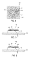
- FIG. 4 shows a plan view including an isolation region of another example of a semiconductor device having a surface conducting channel
- FIG. 5 shows a cross sectional view of another example of a semiconductor device having a surface conducting channel formed on a mesa
- FIG. 6 shows a cross sectional view of another example of a semiconductor device having a surface conducting channel formed on a substrate
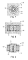
- FIG. 7 shows a plan view of another example of a semiconductor device having a surface conducting channel formed with a gate
- FIG. 8 shows a plan view of another example of a semiconductor device having a surface conducting channel formed with an insulating preservation layer
- FIG. 9 shows a plan view of another example of a semiconductor device having a surface conducting channel formed on a mesa
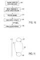
- FIG. 10 shows a flowchart of an example of a method of forming a semiconductor device having a surface conducting channel
- FIG. 11 shows states and transitions between states of a metal oxide layer.
- the electrical properties of metal oxides may be influenced by environmental conditions.
- the atmosphere within which is contained a sample of a metal oxide may affect the conductivity of the sample.
- a sample of ZnO in an ambient atmosphere may exhibit a high resistivity.
- the atmosphere is a vacuum
- the resistivity of the surface of the sample is lower than the resistivity of both the surface and the bulk of the sample in the ambient atmosphere.
- the lower resistivity of the surface of the sample may be preserved by applying a preservation layer to the surface of the sample. When the sample, having a preservation layer applied to the surface, is removed from the vacuum, the lower resistivity of the surface as it was in the vacuum is preserved.
- FIG. 1 is a cross-sectional view of an example of a semiconductor device having a surface conducting channel.
- the semiconductor device 100 includes a metal oxide layer 101, a first and a second channel contact 102 and 103, and a preservation layer 104.
- the metal oxide layer 101 may be a layer of ZnO or MgZnO, for example.
- the metal oxide layer may be a material with a high piezoelectric constant.
- the metal oxide layer 101 includes a surface region 106 and a bulk region 107.
- the surface region 106 includes both the surface of the metal oxide layer 101 and a portion of the bulk of the metal oxide layer directly beneath the surface.
- the surface region 106 may have a lower resistivity due to special treatments and materials properties as discussed below with reference to Fig. 11.
- the preservation layer 104 is formed on a channel area 105.
- the channel area 105 may have the characteristics of the rest of the metal oxide layer 101 resulting from the atmosphere the metal oxide layer 101 is in.
- the preservation layer 104 is formed to preserve the lower resistivity state of the surface of the metal oxide layer 101.
- the area where the lower resistivity state of the surface is preserved is referred to as the channel area 105.
- the channel area 105 is part of the surface region 105.
- the channel area 105 includes not only the surface of the metal oxide layer 101 under the preservation layer 104, but also includes a portion of the metal oxide layer 101 directly beneath that surface.
- the channel area 105 has been labeled an "area", the channel area 105 describes a three dimensional volume beneath the preservation layer 104.
- the channel contacts 102 and 103 are coupled to the channel area 105 of the metal oxide layer 101. Depending on the material of the channel contacts 102 and 103, the channel area 105 may extend beneath the channel contacts 102 and 103.
- the conductivity between the two channel contacts is dominated by the channel area 105. Therefore it can be easily modulated by an exterior electric field.
- the preservation layer 104 may overlap the channel contacts 102 and 103. As a result, the channel area 105 may extend from the first channel contact 102 to the second channel contact 103. Then, connections may be made to the semiconductor device 100 at the channel contacts 102 and 103 to use the channel area 105 under the preservation layer 104.
- the preservation layer 104 is preferably an insulating material.
- the preservation layer 104 may be a dielectric layer formed of SiO x , Ga 2 O 3 , or Si 3 N 4 . (X of SiO x may be real number greater than or equal to one.)
- the preservation layer 104 may also be a variety of oxides, including, for example, GaO 3 , ZnN 3 , TaC, AIN, and BN.
- the preservation layer 104 may be substantially impermeable to gas.
- the conductivity of a surface of a metal oxide may change due to the environmental conditions, particularly the atmosphere. By using the preservation layer 104, a state of the conductivity of the surface may be preserved.
- the preservation layer 104 may prevent molecules from the environment from affecting the channel area 105.
- the preservation layer 104 may be impermeable to some or all of the listed molecules, in addition to other unlisted molecules.
- FIG. 2 shows a plan view of another example of a semiconductor device 200 having a surface conducting channel.
- the first channel contact 102 bounds an area of the surface of the metal oxide layer 101.
- the second channel contact 103 is formed within the area bounded by the first channel contact 102.
- the area between the first and second channel contacts 102 and 103 is covered by the preservation layer 104.
- all of the surface between any part of the channel contacts 102 and 103 is covered by the preservation layer 104.
- first channel contact 102 has been shown as a circular shape in FIG. 2, the first channel contact 102 may be formed in any pattern.
- the first channel contact 102 may be a square, a pentagon, a polygon, or any other continuous path bounding an area of the surface of the metal oxide layer 101.
- FIG. 3 shows a plan view of another example of a semiconductor device 300 having a surface conducting channel.
- An insulating preservation layer 301 may be formed on the surface of the metal oxide layer 101 around the semiconductor device 300.
- the insulating preservation layer 301 preserves the high resistivity state of the metal oxide layer 101, just as the preservation layer 104 preserves the lower resistivity state.
- the channel area 105 is formed under the preservation layer 104 and not the insulating preservation layer 301.
- FIG. 4 shows a plan view of an example of a semiconductor device having a surface conducting channel.
- the semiconductor device 400 may have a region 401.
- the region 401 may be an isolation region.
- the isolation region prevents interaction between the semiconductor device 400 and any adjacent semiconductor devices on the metal oxide layer 101. If the surface of the metal oxide layer 101 between the first channel contact 102 of the semiconductor device 400 and another semiconductor device 400 is not covered by some layer or interrupted by some structure, the resistivity of the surface may change as the environment changes. Thus, adjacent semiconductor devices 400 may be coupled as a result of an environmental change.
- the isolation region prevents this coupling.
- the region 401 may be an insulating preservation layer. As described above, forming an insulating preservation layer in region 401 may preserve the high resistivity of the surface from changing due to the environmental conditions. This insulating preservation layer isolates adjacent semiconductor devices 400 from each other.
- the region 401 which may be the isolation region or the insulating preservation layer have been show not overlapping the first channel contact 102, the isolation region and the insulating preservation layer may overlap the first channel contact 102.
- FIG. 5 shows a cross sectional view of another example of a semiconductor device 500 having a surface conducting channel formed on a mesa 505.
- the semiconductor device 500 may be formed on a mesa 505 of the metal oxide layer 101.
- the mesa 505 is the metal oxide layer 101.
- the substrate 504 may be any non-conductive or semiconductive substrate. Such substrates may include, for example, glass sapphire, or other insulating materials, and layers of such insulating materials formed on other substrates.
- isolations regions and techniques are not required. A connection between a number of semiconductor devices may be desired and the isolation region may not be used between the semiconductor devices. Furthermore, any such isolation region or technique may be used to isolate a set of semiconductor devices from one or more other semiconductor devices.
- FIG. 6 shows a cross sectional view of another example of a semiconductor device 600 having a surface conducting channel formed on a substrate 504.
- the metal oxide layer 101 may be formed on a substrate 504.
- the metal oxide layer 101 may substantially cover a surface of the substrate 504.
- FIG. 7 shows another example of a semiconductor device 700 having a surface conducting channel formed with a gate.
- a gate 701 formed on the preservation layer is formed such that every path from the first channel contact 102 to the second channel contact 103 through the channel area 105 passes under the gate 701.
- the gate 701 may be a circle, smaller in diameter than the first channel contact 102 and larger in diameter than the second channel contact 103. As a result, every path through the channel area 105 passes under the gate 701.
- FIG. 8 illustrating a plan view of another example of a semiconductor device 800 using an insulating preservation layer 402
- the gate 701 is formed across the channel area 105.
- the channel area 105 has been illustrated slightly within the preservation layer 104 and the channel contacts 102 and 103, the boundary of the channel area 105 is for illustration only. Such a channel area 105 may extend to the edges of the preservation layer 104, extend to the edges of the channel contacts 102 and 103, or any combination or sub part of such layers. Since the gate 701 crosses the preservation layer 104, there is no path through the channel area 105 that does not pass under the gate 701.
- the gate 701 overlaps any path through the channel area 105.
- the gate 701 may be formed of a metal or other conductive layer. Thus, a signal may be applied to the gate to modulate the resistivity of the channel area 105 between the channel contacts 102 and 103.
- the gate 701 may be a transparent conductive oxide layer.
- all or portions of the semiconductor device 900 may be transparent.
- the gate 701 may be a biological or chemical gate.
- Biological and chemical sensors used as the gate 701 may allow the semiconductor device to be used, for instance, to detect the presence of certain molecules or ions (e.g., Na+, Ca2+, Cl-, 02, CO2), substances such as glucose or cholesterol, or certain enzymes.
- the gate 701 has been described as being formed over only a portion of the preservation layer 104, the gate 701 may be formed over substantially all of the preservation layer 104. As a result, a signal applied to the gate 701 may affect a larger portion of the channel area 105, increasing the sensitivity of the semiconductor device 900.
- the first channel contact 102 and the second channel contact 103 may be a source contact and a drain contact for a transistor.
- the semiconductor device may form a FET.
- a semiconductor device may include more than two channel contacts and more than one gate.
- FIG. 10 illustrates an example of a method of forming a semiconductor device having a surface conducting channel.
- a metal oxide layer having a surface is provided in 1001.
- a transition is induced in the metal oxide layer in 1004.
- a preservation layer is formed in 1002, defining a channel area of the surface of the metal oxide layer.
- Channel contacts are formed coupled to the channel area in 1003.
- FIG. 11 shows states and transitions between states of a metal oxide layer.
- the metal oxide layer in state S1 is in a higher resistivity state. Such a state S1 may occur when the metal oxide layer is in an atmosphere containing oxygen.
- the metal oxide layer in state S2 has a lower resistivity than in state S1.
- the lower resistivity may be a result of a change of the surface of the metal oxide layer when the metal oxide layer is placed in a different atmosphere, for example, a vacuum.
- Schmidt et. al. "Effects of an Electrically Conducting Layer at the Zinc Oxide Surface", Japanese Journal of Applied Physics, Vol. 44, pp. 7271-7274, October 2005 , describes the transition between different resistivity states on ZnO bulk crystals and is incorporated by reference in its entirety.
- the resistivity of the metal oxide layer depends on the state it is in. For example, if in state S1, the surface of the metal oxide layer is the same as the bulk of the metal oxide layer, then the resistivity of the entire metal oxide layer will be that of the bulk of the metal oxide layer. However, in state S2, the resistivity of the surface of the metal oxide layer may be decreased. Thus, the lower resistivity of the surface may dominate the resistivity of the metal oxide layer, causing the metal oxide layer to have a lower resistivity.
- the metal oxide layer may make a transition from state S1 to state S2 or vice versa.
- Such transitions labeled T1 and T2 respectively, may occur by placing the metal oxide layer in an atmosphere and applying an activation energy, such as heat.
- an activation energy such as heat.
- the metal oxide layer may be placed in a vacuum and heated to cause the transition T1.
- forming the preservation layer in 1002 may include deposition methods such as chemical vapor deposition (CVD), plasma enhanced CVD (PECVD), pulsed laser deposition, molecular beam epitaxy (MBE), and metal organic CVD (MOCVD).
- CVD chemical vapor deposition
- PECVD plasma enhanced CVD
- MBE molecular beam epitaxy
- MOCVD metal organic CVD
- a metal layer may be deposited on the metal oxide layer and subsequently oxidized.
- deposition techniques such as sputtering, or thermal or e-beam evaporation may be used.
- the metal may be oxidized by performing the deposition or annealing the metal in an oxygen rich environment.
- the formation of the preservation layer in 1002 may remove the effect the atmosphere has on the resistivity of the metal oxide layer.
- the state may be preserved from the effects of a different atmosphere. For example, if state S2, the lower resistivity state, is induced in the metal oxide layer, a preservation layer formed on the metal oxide layer will preserve that state under the preservation layer if the atmosphere changes.
- the preservation layer may be formed at the same time the metal oxide layer is changing states.
- a dielectric material may be deposited in a vacuum at high temperatures to both induce the state change and form the preservation layer.
- channel contacts 1003 has been described after forming a preservation layer 1002, one of ordinary skill in the art will understand the order may be any order.
- the channel contacts may be formed on the surface of the metal oxide layer.
- the preservation layer is formed over the surface between the channel contacts to define the channel area.
- the preservation layer may be formed on the metal oxide layer. Then, areas of the preservation layer may be removed to expose the channel area. Channel contacts are then formed in the exposed areas.
- a semiconductor device having a surface conducting channel may have an isolation region.
- Such an isolation region may be formed in 1006 by doping the isolation region to create a high resistivity region.
- the isolation region may be selectively doped with lithium or copper. As a result, the isolation region becomes a high resistivity region, isolating adjacent semiconductor devices from each other.
- the semiconductor device may be formed on a mesa of the metal oxide.
- the metal oxide forming the mesa may be formed in a variety of ways. For example, the mesa may be selectively deposited using a mask defining the mesa. Alternatively, a larger region of the metal oxide may be formed and then selectively etched, leaving the metal oxide mesa.
- an insulating preservation layer may be formed surrounding the semiconductor device.
- an insulating preservation layer such as polyimide
- the insulating preservation layer preserves the non-conductive state of the surface of the metal oxide layer, creating a high resistivity around the semiconductor device.
- polyimide may be deposited to form an insulating preservation layer
- other layers may be deposited, such as organic coatings including self-assembled monolayers such as alkylsiloxanes, fatty acids, and alkanethiolates.
- Another example of a method of forming a semiconductor device having a surface conducting channel may include forming the preservation layer on all areas of the surface of the metal oxide layer between the channel contacts. For example, referring to FIG 7, any path between the channel contacts 102 and 103 passes under the preservation layer 104. Thus each path passes through the channel area 105.
- the semiconductor device may be bounded by an insulating preservation layer as show in FIG. 8. Since the channel area 105 is not disposed substantially under the insulating preservation layer, the channel area is disposed substantially under the preservation layer 104. Thus any path through the channel area 105 passes under the preservation layer.
- the metal oxide layer may be formed on a semiconductor substrate.
- the metal oxide may be deposited on a semiconductor substrate.
- a semiconductor substrate may include silicon, glass, and sapphire.
- a gate may be formed on the preservation layer.
- the gate may be formed such that every path through the channel area is covered by the gate at at least one point.
- the resistivity of all of the channel area may be increase because of the signal applied to the gate. If a path between the channel contacts is not covered, the current may flow through the lower resistivity region not covered by the gate.
- a biological or chemical gate may be formed on the preservation layer.
- the gate may be formed by depositing functionalized molecules that improve adhesion with desired molecules and reduces adhesion with undesired molecules.
- biological or chemical molecules may be absorbed at the gate and modulate the channel area under the gate.
Landscapes
- Engineering & Computer Science (AREA)
- Chemical & Material Sciences (AREA)
- Nanotechnology (AREA)
- Physics & Mathematics (AREA)
- Crystallography & Structural Chemistry (AREA)
- Materials Engineering (AREA)
- General Physics & Mathematics (AREA)
- Condensed Matter Physics & Semiconductors (AREA)
- Composite Materials (AREA)
- Mathematical Physics (AREA)
- Theoretical Computer Science (AREA)
- Thin Film Transistor (AREA)
- Insulated Gate Type Field-Effect Transistor (AREA)
Abstract
Description
- Semiconductor devices include transistors. A transistor may modulate a current flowing through it in response to an input signal. One example of a type of a transistor is a field effect transistor (FET). An FET may change the characteristics of a channel in response to the input signal. The input signal affects the characteristics of the channel such as the carrier concentration and the carrier type. By affecting the characteristics of the channel, the input signal may modulate current flowing through the channel, and hence, flowing through the transistor. Typically, such a transistor may include a source and a drain coupled to the channel. A gate receives the input signal to modulate the channel.
- An FET may also be characterized as an enhancement mode or a depletion mode FET. Enhancement or depletion mode describes the carrier concentrations with no input signal applied. An enhancement mode or a depletion mode FET may also be referred to as a normally off or normally on FET. In a normally on FET, without any input signal applied, the transistor will conduct. Conversely, with a normally off FET, the transistor may not conduct until an input signal is applied.
- Typically, the manufacture of transistors involves several processes. Such processes may include forming a heterostructure using two different semiconductor types, doping a semiconductor to create n and p type regions, and using ion implantation to form the channel of the transistor. These processes add complexity in the manufacturing of a transistor. Furthermore, for some semiconductor types, the creation of a p or n type region may be impracticable.
- An embodiment includes a semiconductor device including a metal oxide layer, a channel area of the metal oxide layer, a preservation layer formed on the channel area of the metal oxide layer, and at least two channel contacts coupled to the channel area of the metal oxide layer.
- A further embodiment includes a method of making a semiconductor device including providing a metal oxide layer having a surface, defining a channel area by forming a preservation layer on the surface, and forming at least two channel contacts coupled to the channel area.
In a further embodiment the metal oxide layer further comprising the metal oxide layer formed on a semiconductor substrate.
In a further embodiment the semiconductor device further comprises a gate formed on the preservation layer substantially over every path between the channel contacts through the preservation layer.
In a further embodiment the gate further comprising at least one selected from the group consisting of a metal layer and a transparent conductive oxide layer.
In a further embodiment the gate further comprising one selected from the group consisting of a biological gate and a chemical gate.
In a further embodiment the preservation layer being substantially impermeable to at least one of a gas, oxygen, nitrogen, and a molecule including a hydroxyl group.
In one embodiment of the method of making a semiconductor device of claim 8, the method further comprises one of the group consisting of: - doping the metal oxide layer to create a high resistivity area outside of the channel area;
- forming a mesa of the metal oxide layer to provide the surface of the metal oxide layer; and
- forming an insulating preservation layer on the surface substantially surrounding the semiconductor device.
- FIG. 1 shows a cross sectional view of an example of a semiconductor device having a surface conducting channel;
- FIG. 2 shows a plan view of another example of a semiconductor device having a surface conducting channel;
- FIG. 3 shows a plan view of another example of a semiconductor device having a surface conducting channel;
- FIG. 4 shows a plan view including an isolation region of another example of a semiconductor device having a surface conducting channel;
- FIG. 5 shows a cross sectional view of another example of a semiconductor device having a surface conducting channel formed on a mesa;
- FIG. 6 shows a cross sectional view of another example of a semiconductor device having a surface conducting channel formed on a substrate;
- FIG. 7 shows a plan view of another example of a semiconductor device having a surface conducting channel formed with a gate;
- FIG. 8 shows a plan view of another example of a semiconductor device having a surface conducting channel formed with an insulating preservation layer;
- FIG. 9 shows a plan view of another example of a semiconductor device having a surface conducting channel formed on a mesa;
- FIG. 10 shows a flowchart of an example of a method of forming a semiconductor device having a surface conducting channel;
- FIG. 11 shows states and transitions between states of a metal oxide layer.
- The electrical properties of metal oxides, such as a high-resistivity zinc oxide (ZnO) may be influenced by environmental conditions. The atmosphere within which is contained a sample of a metal oxide may affect the conductivity of the sample. For example, a sample of ZnO in an ambient atmosphere may exhibit a high resistivity. However, if the atmosphere is a vacuum, the resistivity of the surface of the sample is lower than the resistivity of both the surface and the bulk of the sample in the ambient atmosphere. The lower resistivity of the surface of the sample may be preserved by applying a preservation layer to the surface of the sample. When the sample, having a preservation layer applied to the surface, is removed from the vacuum, the lower resistivity of the surface as it was in the vacuum is preserved.
- FIG. 1 is a cross-sectional view of an example of a semiconductor device having a surface conducting channel. The
semiconductor device 100 includes ametal oxide layer 101, a first and asecond channel contact preservation layer 104. Themetal oxide layer 101 may be a layer of ZnO or MgZnO, for example. In addition, the metal oxide layer may be a material with a high piezoelectric constant. - The
metal oxide layer 101 includes asurface region 106 and abulk region 107. Thesurface region 106 includes both the surface of themetal oxide layer 101 and a portion of the bulk of the metal oxide layer directly beneath the surface. Thesurface region 106 may have a lower resistivity due to special treatments and materials properties as discussed below with reference to Fig. 11. - The
preservation layer 104 is formed on achannel area 105. Before forming thepreservation layer 104, thechannel area 105 may have the characteristics of the rest of themetal oxide layer 101 resulting from the atmosphere themetal oxide layer 101 is in. Thepreservation layer 104 is formed to preserve the lower resistivity state of the surface of themetal oxide layer 101. The area where the lower resistivity state of the surface is preserved is referred to as thechannel area 105. Thechannel area 105 is part of thesurface region 105. Thus, thechannel area 105 includes not only the surface of themetal oxide layer 101 under thepreservation layer 104, but also includes a portion of themetal oxide layer 101 directly beneath that surface. Although thechannel area 105 has been labeled an "area", thechannel area 105 describes a three dimensional volume beneath thepreservation layer 104. Thechannel contacts channel area 105 of themetal oxide layer 101. Depending on the material of thechannel contacts channel area 105 may extend beneath thechannel contacts conductive channel area 105 is close to the surface of themetal oxide layer 101, the conductivity between the two channel contacts is dominated by thechannel area 105. Therefore it can be easily modulated by an exterior electric field. - The
preservation layer 104 may overlap thechannel contacts channel area 105 may extend from thefirst channel contact 102 to thesecond channel contact 103. Then, connections may be made to thesemiconductor device 100 at thechannel contacts channel area 105 under thepreservation layer 104. - The
preservation layer 104 is preferably an insulating material. For example, thepreservation layer 104 may be a dielectric layer formed of SiOx, Ga2O3, or Si3N4. (X of SiOx may be real number greater than or equal to one.) Furthermore, thepreservation layer 104 may also be a variety of oxides, including, for example, GaO3, ZnN3, TaC, AIN, and BN. In addition, thepreservation layer 104 may be substantially impermeable to gas. As described above, the conductivity of a surface of a metal oxide may change due to the environmental conditions, particularly the atmosphere. By using thepreservation layer 104, a state of the conductivity of the surface may be preserved. To achieve this, thepreservation layer 104 may prevent molecules from the environment from affecting thechannel area 105. Particular examples of molecules that thepreservation layer 104 may be impermeable to include oxygen, nitrogen, and molecules including a hydroxyl group. Thepreservation layer 104 may be impermeable to some or all of the listed molecules, in addition to other unlisted molecules. - FIG. 2 shows a plan view of another example of a
semiconductor device 200 having a surface conducting channel. Thefirst channel contact 102 bounds an area of the surface of themetal oxide layer 101. Thesecond channel contact 103 is formed within the area bounded by thefirst channel contact 102. The area between the first andsecond channel contacts preservation layer 104. In this example, all of the surface between any part of thechannel contacts preservation layer 104. - Although
first channel contact 102 has been shown as a circular shape in FIG. 2, thefirst channel contact 102 may be formed in any pattern. For example, thefirst channel contact 102 may be a square, a pentagon, a polygon, or any other continuous path bounding an area of the surface of themetal oxide layer 101. - FIG. 3 shows a plan view of another example of a
semiconductor device 300 having a surface conducting channel. An insulatingpreservation layer 301 may be formed on the surface of themetal oxide layer 101 around thesemiconductor device 300. The insulatingpreservation layer 301 preserves the high resistivity state of themetal oxide layer 101, just as thepreservation layer 104 preserves the lower resistivity state. Thus, thechannel area 105 is formed under thepreservation layer 104 and not the insulatingpreservation layer 301. - FIG. 4 shows a plan view of an example of a semiconductor device having a surface conducting channel. The
semiconductor device 400 may have aregion 401. Theregion 401 may be an isolation region. The isolation region prevents interaction between thesemiconductor device 400 and any adjacent semiconductor devices on themetal oxide layer 101. If the surface of themetal oxide layer 101 between thefirst channel contact 102 of thesemiconductor device 400 and anothersemiconductor device 400 is not covered by some layer or interrupted by some structure, the resistivity of the surface may change as the environment changes. Thus,adjacent semiconductor devices 400 may be coupled as a result of an environmental change. The isolation region prevents this coupling. - Alternatively, the
region 401 may be an insulating preservation layer. As described above, forming an insulating preservation layer inregion 401 may preserve the high resistivity of the surface from changing due to the environmental conditions. This insulating preservation layer isolatesadjacent semiconductor devices 400 from each other. - Although the
region 401 which may be the isolation region or the insulating preservation layer have been show not overlapping thefirst channel contact 102, the isolation region and the insulating preservation layer may overlap thefirst channel contact 102. - FIG. 5 shows a cross sectional view of another example of a
semiconductor device 500 having a surface conducting channel formed on amesa 505. Instead of forming thesemiconductor device 500 on a plane of ametal oxide layer 101, thesemiconductor device 500 may be formed on amesa 505 of themetal oxide layer 101. Themesa 505 is themetal oxide layer 101. Thus, if adjacent semiconductor devices are formed onindividual mesas 505, thesemiconductor devices 500 are isolated from each other. Themesa 505 may be formed on asubstrate 504. Thesubstrate 504 may be any non-conductive or semiconductive substrate. Such substrates may include, for example, glass sapphire, or other insulating materials, and layers of such insulating materials formed on other substrates. - Although several structures isolating semiconductor devices from each other have been described, such isolations regions and techniques are not required. A connection between a number of semiconductor devices may be desired and the isolation region may not be used between the semiconductor devices. Furthermore, any such isolation region or technique may be used to isolate a set of semiconductor devices from one or more other semiconductor devices.
- FIG. 6 shows a cross sectional view of another example of a
semiconductor device 600 having a surface conducting channel formed on asubstrate 504. Referring to FIG. 6, just as themesa 505 may be formed on asubstrate 504, themetal oxide layer 101 may be formed on asubstrate 504. Themetal oxide layer 101 may substantially cover a surface of thesubstrate 504. - FIG. 7 shows another example of a
semiconductor device 700 having a surface conducting channel formed with a gate. Preferably, agate 701 formed on the preservation layer is formed such that every path from thefirst channel contact 102 to thesecond channel contact 103 through thechannel area 105 passes under thegate 701. In the example illustrated in FIG. 7, thegate 701 may be a circle, smaller in diameter than thefirst channel contact 102 and larger in diameter than thesecond channel contact 103. As a result, every path through thechannel area 105 passes under thegate 701. - Alternatively, as shown in FIG. 8, illustrating a plan view of another example of a
semiconductor device 800 using an insulatingpreservation layer 402, thegate 701 is formed across thechannel area 105. Although thechannel area 105 has been illustrated slightly within thepreservation layer 104 and thechannel contacts channel area 105 is for illustration only. Such achannel area 105 may extend to the edges of thepreservation layer 104, extend to the edges of thechannel contacts gate 701 crosses thepreservation layer 104, there is no path through thechannel area 105 that does not pass under thegate 701. - In addition, as shown in FIG. 9, illustrating a semiconductor device using a mesa as an isolating technique, the
gate 701 overlaps any path through thechannel area 105. - The
gate 701 may be formed of a metal or other conductive layer. Thus, a signal may be applied to the gate to modulate the resistivity of thechannel area 105 between thechannel contacts - Alternatively, the
gate 701 may be a transparent conductive oxide layer. As a result, depending on the transparency of the other portions of thesemiconductor device 900, all or portions of thesemiconductor device 900 may be transparent. - In addition, the
gate 701 may be a biological or chemical gate. Biological and chemical sensors used as thegate 701 may allow the semiconductor device to be used, for instance, to detect the presence of certain molecules or ions (e.g., Na+, Ca2+, Cl-, 02, CO2), substances such as glucose or cholesterol, or certain enzymes. - Although the
gate 701 has been described as being formed over only a portion of thepreservation layer 104, thegate 701 may be formed over substantially all of thepreservation layer 104. As a result, a signal applied to thegate 701 may affect a larger portion of thechannel area 105, increasing the sensitivity of thesemiconductor device 900. - In another example, the
first channel contact 102 and thesecond channel contact 103 may be a source contact and a drain contact for a transistor. Thus, the semiconductor device may form a FET. - Although two
channel contacts - FIG. 10 illustrates an example of a method of forming a semiconductor device having a surface conducting channel. A metal oxide layer having a surface is provided in 1001. A transition is induced in the metal oxide layer in 1004. A preservation layer is formed in 1002, defining a channel area of the surface of the metal oxide layer. Channel contacts are formed coupled to the channel area in 1003.
- Inducing the transition of the metal oxide layer in 1004 may cause the resistivity of the metal oxide layer to become less resistive. FIG. 11 shows states and transitions between states of a metal oxide layer. The metal oxide layer in state S1 is in a higher resistivity state. Such a state S1 may occur when the metal oxide layer is in an atmosphere containing oxygen. The metal oxide layer in state S2 has a lower resistivity than in state S1. The lower resistivity may be a result of a change of the surface of the metal oxide layer when the metal oxide layer is placed in a different atmosphere, for example, a vacuum. For example, Schmidt et. al., "Effects of an Electrically Conducting Layer at the Zinc Oxide Surface", Japanese Journal of Applied Physics, Vol. 44, pp. 7271-7274, October 2005, describes the transition between different resistivity states on ZnO bulk crystals and is incorporated by reference in its entirety.
- Thus, the resistivity of the metal oxide layer depends on the state it is in. For example, if in state S1, the surface of the metal oxide layer is the same as the bulk of the metal oxide layer, then the resistivity of the entire metal oxide layer will be that of the bulk of the metal oxide layer. However, in state S2, the resistivity of the surface of the metal oxide layer may be decreased. Thus, the lower resistivity of the surface may dominate the resistivity of the metal oxide layer, causing the metal oxide layer to have a lower resistivity.
- The metal oxide layer may make a transition from state S1 to state S2 or vice versa. Such transitions, labeled T1 and T2 respectively, may occur by placing the metal oxide layer in an atmosphere and applying an activation energy, such as heat. For example if state S2 is desired, the metal oxide layer may be placed in a vacuum and heated to cause the transition T1.
- Referring to FIG. 10, forming the preservation layer in 1002 may include deposition methods such as chemical vapor deposition (CVD), plasma enhanced CVD (PECVD), pulsed laser deposition, molecular beam epitaxy (MBE), and metal organic CVD (MOCVD). In addition, a metal layer may be deposited on the metal oxide layer and subsequently oxidized. For example, deposition techniques such as sputtering, or thermal or e-beam evaporation may be used. The metal may be oxidized by performing the deposition or annealing the metal in an oxygen rich environment.
- The formation of the preservation layer in 1002 may remove the effect the atmosphere has on the resistivity of the metal oxide layer. Thus, after inducing a state transition of the metal oxide layer to a desired state, the state may be preserved from the effects of a different atmosphere. For example, if state S2, the lower resistivity state, is induced in the metal oxide layer, a preservation layer formed on the metal oxide layer will preserve that state under the preservation layer if the atmosphere changes.
- Although inducing a state transition has been described before forming a preservation layer, the preservation layer may be formed at the same time the metal oxide layer is changing states. For example, a dielectric material may be deposited in a vacuum at high temperatures to both induce the state change and form the preservation layer.
- Although forming
channel contacts 1003 has been described after forming apreservation layer 1002, one of ordinary skill in the art will understand the order may be any order. For example, the channel contacts may be formed on the surface of the metal oxide layer. Then, the preservation layer is formed over the surface between the channel contacts to define the channel area. - Alternatively, the preservation layer may be formed on the metal oxide layer. Then, areas of the preservation layer may be removed to expose the channel area. Channel contacts are then formed in the exposed areas.
- Although some methods and sequences to define a channel area and form channel contacts have been described, one of ordinary skill in the art will appreciate that other methods may be used that result in a defined channel area and channel contacts coupled to the channel area.
- As described above, a semiconductor device having a surface conducting channel may have an isolation region. Such an isolation region may be formed in 1006 by doping the isolation region to create a high resistivity region. For example, the isolation region may be selectively doped with lithium or copper. As a result, the isolation region becomes a high resistivity region, isolating adjacent semiconductor devices from each other.
- In addition, as described above, the semiconductor device may be formed on a mesa of the metal oxide. The metal oxide forming the mesa may be formed in a variety of ways. For example, the mesa may be selectively deposited using a mask defining the mesa. Alternatively, a larger region of the metal oxide may be formed and then selectively etched, leaving the metal oxide mesa.
- Furthermore, an insulating preservation layer may be formed surrounding the semiconductor device. For example, an insulating preservation layer, such as polyimide, may be deposited along the perimeter of the semiconductor device. The insulating preservation layer preserves the non-conductive state of the surface of the metal oxide layer, creating a high resistivity around the semiconductor device. Although polyimide may be deposited to form an insulating preservation layer, other layers may be deposited, such as organic coatings including self-assembled monolayers such as alkylsiloxanes, fatty acids, and alkanethiolates.
- Another example of a method of forming a semiconductor device having a surface conducting channel may include forming the preservation layer on all areas of the surface of the metal oxide layer between the channel contacts. For example, referring to FIG 7, any path between the
channel contacts preservation layer 104. Thus each path passes through thechannel area 105. - In addition, the semiconductor device may be bounded by an insulating preservation layer as show in FIG. 8. Since the
channel area 105 is not disposed substantially under the insulating preservation layer, the channel area is disposed substantially under thepreservation layer 104. Thus any path through thechannel area 105 passes under the preservation layer. - In another example of a method of forming a semiconductor device having a surface conducting channel, the metal oxide layer may be formed on a semiconductor substrate. For example, the metal oxide may be deposited on a semiconductor substrate. Such a semiconductor substrate may include silicon, glass, and sapphire.
- As described above, a gate may be formed on the preservation layer. Preferably, the gate may be formed such that every path through the channel area is covered by the gate at at least one point. Thus, since such a semiconductor device may be normally on, the resistivity of all of the channel area may be increase because of the signal applied to the gate. If a path between the channel contacts is not covered, the current may flow through the lower resistivity region not covered by the gate.
- As described above, a biological or chemical gate may be formed on the preservation layer. The gate may be formed by depositing functionalized molecules that improve adhesion with desired molecules and reduces adhesion with undesired molecules. Thus, biological or chemical molecules may be absorbed at the gate and modulate the channel area under the gate.
In a further embodiment providing the surface of the metal oxide layer further comprising forming the metal oxide layer on a semiconductor substrate.
In a further embodiment the method further comprises forming a gate on the preservation layer substantially over every path over the preservation layer between the channel contacts.
In a further embodiment forming a gate further comprises forming at least one selected from the group consisting of a metal gate, a transparent conducting metal oxide, a biological gate, and a chemical gate.
Claims (10)
- A semiconductor device comprising:a metal oxide layer having a surface region and a bulk region;a channel area of the surface region of the metal oxide layer having a resistivity lower than a resistivity of the bulk region of the metal oxide layer;a preservation layer formed on the channel area; andat least two channel contacts coupled to the channel area of the metal oxide layer.
- The semiconductor device of claim 1, the metal oxide layer further comprising one selected from the group consisting of a zinc oxide layer and a magnesium zinc oxide layer.
- The semiconductor device of claim 1, the preservation layer overlapping the channel contacts.
- The semiconductor device of claim 1, the channel contacts further comprising:a source contact; anda drain contact.
- The semiconductor device of claim 1, wherein all of a surface of the metal oxide layer disposed between any two of the channel contacts is covered by the preservation layer.
- The semiconductor device of claim 1, further comprising one selected from the group consisting of:an isolation region in the metal oxide layer surrounding the preservation layer and the at least two channel contacts;an insulating preservation layer on the surface substantially surrounding the semiconductor device; andthe metal oxide layer further comprising a mesa of the metal oxide.
- The semiconductor device of claim 6, wherein the insulating preservation layer further comprises at least one selected from the group consisting of polyimide and a self-assembled monolayer.
- A method of making a semiconductor device comprising:providing a metal oxide layer having a surface;inducing the metal oxide layer to transition to a surface conducting state;forming a preservation layer on at least a part of the surface to define a channel area; andforming at least two channel contacts coupled to the channel area.
- The method of making a semiconductor device of claim 8, providing the metal oxide layer further comprises one selected from the group consisting of providing a zinc oxide layer and providing a magnesium zinc oxide layer.
- The method of making a semiconductor device of claim 8, forming the channel contacts further comprising:removing an area of the preservation layer for each channel contact;forming each channel contact on the respective area removed from the preservation layer.
Applications Claiming Priority (1)
| Application Number | Priority Date | Filing Date | Title |
|---|---|---|---|
| US11/313,341 US7314801B2 (en) | 2005-12-20 | 2005-12-20 | Semiconductor device having a surface conducting channel and method of forming |
Publications (1)
| Publication Number | Publication Date |
|---|---|
| EP1801887A1 true EP1801887A1 (en) | 2007-06-27 |
Family
ID=37776421
Family Applications (1)
| Application Number | Title | Priority Date | Filing Date |
|---|---|---|---|
| EP06126360A Withdrawn EP1801887A1 (en) | 2005-12-20 | 2006-12-18 | Semiconductor device having a surface conducting channel and method of forming |
Country Status (3)
| Country | Link |
|---|---|
| US (1) | US7314801B2 (en) |
| EP (1) | EP1801887A1 (en) |
| JP (2) | JP2007173820A (en) |
Cited By (4)
| Publication number | Priority date | Publication date | Assignee | Title |
|---|---|---|---|---|
| US9647131B2 (en) | 2009-09-24 | 2017-05-09 | Semiconductor Energy Laboratory Co., Ltd. | Semiconductor device, power circuit, and manufacturing method of semiconductor device |
| US9865744B2 (en) | 2010-01-22 | 2018-01-09 | Semiconductor Energy Laboratory Co., Ltd. | Semiconductor device |
| US9959822B2 (en) | 2009-10-16 | 2018-05-01 | Semiconductor Energy Laboratory Co., Ltd. | Liquid crystal display device and electronic device including the liquid crystal display device |
| US11107396B2 (en) | 2009-10-21 | 2021-08-31 | Semiconductor Energy Laboratory Co., Ltd. | Display device and electronic device including thin film transistor including top-gate |
Families Citing this family (4)
| Publication number | Priority date | Publication date | Assignee | Title |
|---|---|---|---|---|
| JP5116225B2 (en) * | 2005-09-06 | 2013-01-09 | キヤノン株式会社 | Manufacturing method of oxide semiconductor device |
| KR101844080B1 (en) * | 2009-10-16 | 2018-03-30 | 가부시키가이샤 한도오따이 에네루기 켄큐쇼 | Liquid crystal display device and electronic apparatus having the same |
| WO2011068025A1 (en) * | 2009-12-04 | 2011-06-09 | Semiconductor Energy Laboratory Co., Ltd. | Dc converter circuit and power supply circuit |
| US8610180B2 (en) * | 2010-06-11 | 2013-12-17 | Semiconductor Energy Laboratory Co., Ltd. | Gas sensor and method for manufacturing the gas sensor |
Citations (3)
| Publication number | Priority date | Publication date | Assignee | Title |
|---|---|---|---|---|
| WO2004114391A1 (en) * | 2003-06-20 | 2004-12-29 | Sharp Kabushiki Kaisha | Semiconductor device, its manufacturing method, and electronic device |
| EP1544907A1 (en) * | 2003-12-17 | 2005-06-22 | Hewlett-Packard Development Company, L.P. | Transistor device having p-type delafossite channel |
| WO2005074038A1 (en) * | 2004-01-23 | 2005-08-11 | Hewlett-Packard Development Company, L.P. | Transistor including a deposited channel region having a doped portion |
Family Cites Families (9)
| Publication number | Priority date | Publication date | Assignee | Title |
|---|---|---|---|---|
| JPH0727899B2 (en) * | 1986-10-20 | 1995-03-29 | 日本電気株式会社 | Method for forming silicon nitride film |
| GB2361480B (en) * | 2000-04-19 | 2002-06-19 | Murata Manufacturing Co | Method for forming p-type semiconductor film and light emitting device using the same |
| JP4090716B2 (en) * | 2001-09-10 | 2008-05-28 | 雅司 川崎 | Thin film transistor and matrix display device |
| CN1445821A (en) * | 2002-03-15 | 2003-10-01 | 三洋电机株式会社 | Forming method of ZnO film and ZnO semiconductor layer, semiconductor element and manufacturing method thereof |
| JP2004006686A (en) * | 2002-03-26 | 2004-01-08 | Sanyo Electric Co Ltd | Method for forming ZnO semiconductor layer, method for manufacturing semiconductor element, and semiconductor element |
| US7339187B2 (en) * | 2002-05-21 | 2008-03-04 | State Of Oregon Acting By And Through The Oregon State Board Of Higher Education On Behalf Of Oregon State University | Transistor structures |
| EP2413366B1 (en) * | 2004-03-12 | 2017-01-11 | Japan Science And Technology Agency | A switching element of LCDs or organic EL displays |
| JP4461873B2 (en) * | 2004-03-29 | 2010-05-12 | カシオ計算機株式会社 | Zinc oxide processing method and thin film transistor manufacturing method |
| JP2006005116A (en) * | 2004-06-17 | 2006-01-05 | Casio Comput Co Ltd | Film forming method, semiconductor film, and laminated insulating film |
-
2005
- 2005-12-20 US US11/313,341 patent/US7314801B2/en not_active Expired - Fee Related
-
2006
- 2006-12-18 EP EP06126360A patent/EP1801887A1/en not_active Withdrawn
- 2006-12-19 JP JP2006340835A patent/JP2007173820A/en active Pending
-
2013
- 2013-12-06 JP JP2013252609A patent/JP2014075601A/en not_active Ceased
Patent Citations (4)
| Publication number | Priority date | Publication date | Assignee | Title |
|---|---|---|---|---|
| WO2004114391A1 (en) * | 2003-06-20 | 2004-12-29 | Sharp Kabushiki Kaisha | Semiconductor device, its manufacturing method, and electronic device |
| US20060244107A1 (en) * | 2003-06-20 | 2006-11-02 | Toshinori Sugihara | Semiconductor device, manufacturing method, and electronic device |
| EP1544907A1 (en) * | 2003-12-17 | 2005-06-22 | Hewlett-Packard Development Company, L.P. | Transistor device having p-type delafossite channel |
| WO2005074038A1 (en) * | 2004-01-23 | 2005-08-11 | Hewlett-Packard Development Company, L.P. | Transistor including a deposited channel region having a doped portion |
Non-Patent Citations (4)
| Title |
|---|
| HONG DAVID ET AL: "Passivation of zinc-tin-oxide thin-film transistors", JOURNAL OF VACUUM SCIENCE AND TECHNOLOGY. B, MICROELECTRONICS AND NANOMETER STRUCTURES PROCESSING, MEASUREMENT AND PHENOMENA, AMERICAN INSTITUTE OF PHYSICS, NEW YORK, NY, US, vol. 23, no. 6, 29 November 2005 (2005-11-29), pages 25 - 27, XP012080342, ISSN: 1071-1023 * |
| KWON Y ET AL: "Enhancement-mode thin-film field-effect transistor using phosphorus-doped (Zn,Mg)O channel", APPLIED PHYSICS LETTERS, AIP, AMERICAN INSTITUTE OF PHYSICS, MELVILLE, NY, US, vol. 84, no. 14, 5 April 2004 (2004-04-05), pages 2685 - 2687, XP012061036, ISSN: 0003-6951 * |
| LOOK ET AL: "Effects of surface conduction on Hall-effect measurements in ZnO", SUPERLATTICES AND MICROSTRUCTURES, ACADEMIC PRESS, LONDON, GB, vol. 38, no. 4-6, October 2005 (2005-10-01), pages 406 - 412, XP005153769, ISSN: 0749-6036 * |
| O. SCHMIDT, P. KIESEL, C. G. VAN DE WALLE, N. M. JOHNSON, J. NAUSE, G. H. DOEHLER: "Effects of an Electrically Conducting Layer at the Zinc Oxide Surface", JAPANESE JOURNAL OF APPLIED PHYSICS, vol. 44, no. 10, 11 October 2005 (2005-10-11), pages 7271 - 7274, XP001090590 * |
Cited By (7)
| Publication number | Priority date | Publication date | Assignee | Title |
|---|---|---|---|---|
| US9647131B2 (en) | 2009-09-24 | 2017-05-09 | Semiconductor Energy Laboratory Co., Ltd. | Semiconductor device, power circuit, and manufacturing method of semiconductor device |
| US9959822B2 (en) | 2009-10-16 | 2018-05-01 | Semiconductor Energy Laboratory Co., Ltd. | Liquid crystal display device and electronic device including the liquid crystal display device |
| US10565946B2 (en) | 2009-10-16 | 2020-02-18 | Semiconductor Energy Laboratory Co., Ltd. | Liquid crystal display device and electronic device including the liquid crystal display device |
| US11107396B2 (en) | 2009-10-21 | 2021-08-31 | Semiconductor Energy Laboratory Co., Ltd. | Display device and electronic device including thin film transistor including top-gate |
| US12067934B2 (en) | 2009-10-21 | 2024-08-20 | Semiconductor Energy Laboratory Co., Ltd. | Display device and electronic device including display device |
| US12347368B2 (en) | 2009-10-21 | 2025-07-01 | Semiconductor Energy Laboratory Co., Ltd. | Semiconductor device and electronic device including semiconductor device |
| US9865744B2 (en) | 2010-01-22 | 2018-01-09 | Semiconductor Energy Laboratory Co., Ltd. | Semiconductor device |
Also Published As
| Publication number | Publication date |
|---|---|
| US20070141789A1 (en) | 2007-06-21 |
| US7314801B2 (en) | 2008-01-01 |
| JP2014075601A (en) | 2014-04-24 |
| JP2007173820A (en) | 2007-07-05 |
Similar Documents
| Publication | Publication Date | Title |
|---|---|---|
| JP2014075601A (en) | Method for manufacturing semiconductor device | |
| US7026713B2 (en) | Transistor device having a delafossite material | |
| KR101410926B1 (en) | Thin film transistor and manufacturing method thereof | |
| KR101413655B1 (en) | Method for manufacturing oxide semiconductor thin film transistor | |
| US8101947B2 (en) | System and method for manufacturing a thin-film device | |
| KR101344483B1 (en) | Thin film transistor | |
| KR20080094483A (en) | Thin film transistor having a selectively crystallized channel layer and its manufacturing method | |
| JP2007081362A (en) | Transparent thin film transistor and manufacturing method thereof | |
| KR20100061555A (en) | Method for manufacturing field-effect transistor | |
| US6955932B2 (en) | Single and double-gate pseudo-FET devices for semiconductor materials evaluation | |
| JP2007305658A (en) | Oxide transistor and manufacturing method thereof | |
| CN104037087A (en) | Method for manufacturing semiconductor device on substrate and semiconductor device | |
| WO2015165174A1 (en) | Thin film transistor and manufacturing method therefor, display substrate, and display device | |
| US9070779B2 (en) | Metal oxide TFT with improved temperature stability | |
| KR101802054B1 (en) | Oxide semiconductor thin film transistor and method for manufacturing thereof | |
| JP4661065B2 (en) | Complementary organic semiconductor device | |
| JPH03217059A (en) | Thin film transistor | |
| KR102875719B1 (en) | Integrated circuit device and method for manufacturing the same | |
| US5311045A (en) | Field effect devices with ultra-short gates | |
| Nayfeh et al. | Formation of Single Tiers of Bridging Silicon Nanowires for Transistor Applications Using Vapor–Liquid–Solid Growth from Short Silicon‐on‐Insulator Sidewalls | |
| KR102697352B1 (en) | Method for manufacturing oxide thin film transistor | |
| US7115898B2 (en) | Organic semiconductor device, RF modulation circuit, and IC card | |
| JPS628575A (en) | Semiconductor device | |
| JPS5955074A (en) | Manufacture of semiconductor integrated circuit device | |
| JPH0864887A (en) | GaAs Hall element |
Legal Events
| Date | Code | Title | Description |
|---|---|---|---|
| PUAI | Public reference made under article 153(3) epc to a published international application that has entered the european phase |
Free format text: ORIGINAL CODE: 0009012 |
|
| AK | Designated contracting states |
Kind code of ref document: A1 Designated state(s): AT BE BG CH CY CZ DE DK EE ES FI FR GB GR HU IE IS IT LI LT LU LV MC NL PL PT RO SE SI SK TR |
|
| AX | Request for extension of the european patent |
Extension state: AL BA HR MK YU |
|
| 17P | Request for examination filed |
Effective date: 20071227 |
|
| 17Q | First examination report despatched |
Effective date: 20080131 |
|
| AKX | Designation fees paid |
Designated state(s): DE FR GB |
|
| STAA | Information on the status of an ep patent application or granted ep patent |
Free format text: STATUS: THE APPLICATION IS DEEMED TO BE WITHDRAWN |
|
| 18D | Application deemed to be withdrawn |
Effective date: 20160701 |