EP1801849A2 - Semiconductor device, method of manufacturing the same, and camera module - Google Patents
Semiconductor device, method of manufacturing the same, and camera module Download PDFInfo
- Publication number
- EP1801849A2 EP1801849A2 EP06026547A EP06026547A EP1801849A2 EP 1801849 A2 EP1801849 A2 EP 1801849A2 EP 06026547 A EP06026547 A EP 06026547A EP 06026547 A EP06026547 A EP 06026547A EP 1801849 A2 EP1801849 A2 EP 1801849A2
- Authority
- EP
- European Patent Office
- Prior art keywords
- supporting body
- semiconductor substrate
- semiconductor device
- light receiving
- pad electrode
- Prior art date
- Legal status (The legal status is an assumption and is not a legal conclusion. Google has not performed a legal analysis and makes no representation as to the accuracy of the status listed.)
- Withdrawn
Links
Images







Classifications
-
- H—ELECTRICITY
- H10—SEMICONDUCTOR DEVICES; ELECTRIC SOLID-STATE DEVICES NOT OTHERWISE PROVIDED FOR
- H10W—GENERIC PACKAGES, INTERCONNECTIONS, CONNECTORS OR OTHER CONSTRUCTIONAL DETAILS OF DEVICES COVERED BY CLASS H10
- H10W76/00—Containers; Fillings or auxiliary members therefor; Seals
- H10W76/10—Containers or parts thereof
-
- H—ELECTRICITY
- H10—SEMICONDUCTOR DEVICES; ELECTRIC SOLID-STATE DEVICES NOT OTHERWISE PROVIDED FOR
- H10F—INORGANIC SEMICONDUCTOR DEVICES SENSITIVE TO INFRARED RADIATION, LIGHT, ELECTROMAGNETIC RADIATION OF SHORTER WAVELENGTH OR CORPUSCULAR RADIATION
- H10F39/00—Integrated devices, or assemblies of multiple devices, comprising at least one element covered by group H10F30/00, e.g. radiation detectors comprising photodiode arrays
- H10F39/80—Constructional details of image sensors
- H10F39/804—Containers or encapsulations
-
- H—ELECTRICITY
- H04—ELECTRIC COMMUNICATION TECHNIQUE
- H04N—PICTORIAL COMMUNICATION, e.g. TELEVISION
- H04N23/00—Cameras or camera modules comprising electronic image sensors; Control thereof
- H04N23/57—Mechanical or electrical details of cameras or camera modules specially adapted for being embedded in other devices
-
- H—ELECTRICITY
- H10—SEMICONDUCTOR DEVICES; ELECTRIC SOLID-STATE DEVICES NOT OTHERWISE PROVIDED FOR
- H10F—INORGANIC SEMICONDUCTOR DEVICES SENSITIVE TO INFRARED RADIATION, LIGHT, ELECTROMAGNETIC RADIATION OF SHORTER WAVELENGTH OR CORPUSCULAR RADIATION
- H10F39/00—Integrated devices, or assemblies of multiple devices, comprising at least one element covered by group H10F30/00, e.g. radiation detectors comprising photodiode arrays
- H10F39/011—Manufacture or treatment of image sensors covered by group H10F39/12
- H10F39/026—Wafer-level processing
-
- H—ELECTRICITY
- H10—SEMICONDUCTOR DEVICES; ELECTRIC SOLID-STATE DEVICES NOT OTHERWISE PROVIDED FOR
- H10W—GENERIC PACKAGES, INTERCONNECTIONS, CONNECTORS OR OTHER CONSTRUCTIONAL DETAILS OF DEVICES COVERED BY CLASS H10
- H10W74/00—Encapsulations, e.g. protective coatings
- H10W74/10—Encapsulations, e.g. protective coatings characterised by their shape or disposition
- H10W74/131—Encapsulations, e.g. protective coatings characterised by their shape or disposition the semiconductor body being only partially enclosed
- H10W74/144—Encapsulations, e.g. protective coatings characterised by their shape or disposition the semiconductor body being only partially enclosed the encapsulations comprising foils
-
- H—ELECTRICITY
- H10—SEMICONDUCTOR DEVICES; ELECTRIC SOLID-STATE DEVICES NOT OTHERWISE PROVIDED FOR
- H10W—GENERIC PACKAGES, INTERCONNECTIONS, CONNECTORS OR OTHER CONSTRUCTIONAL DETAILS OF DEVICES COVERED BY CLASS H10
- H10W72/00—Interconnections or connectors in packages
- H10W72/01—Manufacture or treatment
- H10W72/012—Manufacture or treatment of bump connectors, dummy bumps or thermal bumps
- H10W72/01221—Manufacture or treatment of bump connectors, dummy bumps or thermal bumps using local deposition
- H10W72/01223—Manufacture or treatment of bump connectors, dummy bumps or thermal bumps using local deposition in liquid form, e.g. by dispensing droplets or by screen printing
-
- H—ELECTRICITY
- H10—SEMICONDUCTOR DEVICES; ELECTRIC SOLID-STATE DEVICES NOT OTHERWISE PROVIDED FOR
- H10W—GENERIC PACKAGES, INTERCONNECTIONS, CONNECTORS OR OTHER CONSTRUCTIONAL DETAILS OF DEVICES COVERED BY CLASS H10
- H10W72/00—Interconnections or connectors in packages
- H10W72/01—Manufacture or treatment
- H10W72/012—Manufacture or treatment of bump connectors, dummy bumps or thermal bumps
- H10W72/01231—Manufacture or treatment of bump connectors, dummy bumps or thermal bumps using blanket deposition
- H10W72/01233—Manufacture or treatment of bump connectors, dummy bumps or thermal bumps using blanket deposition in liquid form, e.g. spin coating, spray coating or immersion coating
- H10W72/01235—Manufacture or treatment of bump connectors, dummy bumps or thermal bumps using blanket deposition in liquid form, e.g. spin coating, spray coating or immersion coating by plating, e.g. electroless plating or electroplating
-
- H—ELECTRICITY
- H10—SEMICONDUCTOR DEVICES; ELECTRIC SOLID-STATE DEVICES NOT OTHERWISE PROVIDED FOR
- H10W—GENERIC PACKAGES, INTERCONNECTIONS, CONNECTORS OR OTHER CONSTRUCTIONAL DETAILS OF DEVICES COVERED BY CLASS H10
- H10W72/00—Interconnections or connectors in packages
- H10W72/01—Manufacture or treatment
- H10W72/012—Manufacture or treatment of bump connectors, dummy bumps or thermal bumps
- H10W72/01251—Changing the shapes of bumps
- H10W72/01255—Changing the shapes of bumps by using masks
-
- H—ELECTRICITY
- H10—SEMICONDUCTOR DEVICES; ELECTRIC SOLID-STATE DEVICES NOT OTHERWISE PROVIDED FOR
- H10W—GENERIC PACKAGES, INTERCONNECTIONS, CONNECTORS OR OTHER CONSTRUCTIONAL DETAILS OF DEVICES COVERED BY CLASS H10
- H10W72/00—Interconnections or connectors in packages
- H10W72/01—Manufacture or treatment
- H10W72/012—Manufacture or treatment of bump connectors, dummy bumps or thermal bumps
- H10W72/01251—Changing the shapes of bumps
- H10W72/01257—Changing the shapes of bumps by reflowing
-
- H—ELECTRICITY
- H10—SEMICONDUCTOR DEVICES; ELECTRIC SOLID-STATE DEVICES NOT OTHERWISE PROVIDED FOR
- H10W—GENERIC PACKAGES, INTERCONNECTIONS, CONNECTORS OR OTHER CONSTRUCTIONAL DETAILS OF DEVICES COVERED BY CLASS H10
- H10W72/00—Interconnections or connectors in packages
- H10W72/071—Connecting or disconnecting
- H10W72/072—Connecting or disconnecting of bump connectors
- H10W72/07221—Aligning
- H10W72/07227—Aligning involving guiding structures, e.g. spacers or supporting members
-
- H—ELECTRICITY
- H10—SEMICONDUCTOR DEVICES; ELECTRIC SOLID-STATE DEVICES NOT OTHERWISE PROVIDED FOR
- H10W—GENERIC PACKAGES, INTERCONNECTIONS, CONNECTORS OR OTHER CONSTRUCTIONAL DETAILS OF DEVICES COVERED BY CLASS H10
- H10W72/00—Interconnections or connectors in packages
- H10W72/20—Bump connectors, e.g. solder bumps or copper pillars; Dummy bumps; Thermal bumps
- H10W72/241—Dispositions, e.g. layouts
- H10W72/242—Dispositions, e.g. layouts relative to the surface, e.g. recessed, protruding
-
- H—ELECTRICITY
- H10—SEMICONDUCTOR DEVICES; ELECTRIC SOLID-STATE DEVICES NOT OTHERWISE PROVIDED FOR
- H10W—GENERIC PACKAGES, INTERCONNECTIONS, CONNECTORS OR OTHER CONSTRUCTIONAL DETAILS OF DEVICES COVERED BY CLASS H10
- H10W72/00—Interconnections or connectors in packages
- H10W72/20—Bump connectors, e.g. solder bumps or copper pillars; Dummy bumps; Thermal bumps
- H10W72/241—Dispositions, e.g. layouts
- H10W72/247—Dispositions of multiple bumps
- H10W72/248—Top-view layouts, e.g. mirror arrays
-
- H—ELECTRICITY
- H10—SEMICONDUCTOR DEVICES; ELECTRIC SOLID-STATE DEVICES NOT OTHERWISE PROVIDED FOR
- H10W—GENERIC PACKAGES, INTERCONNECTIONS, CONNECTORS OR OTHER CONSTRUCTIONAL DETAILS OF DEVICES COVERED BY CLASS H10
- H10W72/00—Interconnections or connectors in packages
- H10W72/20—Bump connectors, e.g. solder bumps or copper pillars; Dummy bumps; Thermal bumps
- H10W72/251—Materials
- H10W72/252—Materials comprising solid metals or solid metalloids, e.g. PbSn, Ag or Cu
-
- H—ELECTRICITY
- H10—SEMICONDUCTOR DEVICES; ELECTRIC SOLID-STATE DEVICES NOT OTHERWISE PROVIDED FOR
- H10W—GENERIC PACKAGES, INTERCONNECTIONS, CONNECTORS OR OTHER CONSTRUCTIONAL DETAILS OF DEVICES COVERED BY CLASS H10
- H10W72/00—Interconnections or connectors in packages
- H10W72/20—Bump connectors, e.g. solder bumps or copper pillars; Dummy bumps; Thermal bumps
- H10W72/281—Auxiliary members
- H10W72/283—Reinforcing structures, e.g. bump collars
-
- H—ELECTRICITY
- H10—SEMICONDUCTOR DEVICES; ELECTRIC SOLID-STATE DEVICES NOT OTHERWISE PROVIDED FOR
- H10W—GENERIC PACKAGES, INTERCONNECTIONS, CONNECTORS OR OTHER CONSTRUCTIONAL DETAILS OF DEVICES COVERED BY CLASS H10
- H10W72/00—Interconnections or connectors in packages
- H10W72/20—Bump connectors, e.g. solder bumps or copper pillars; Dummy bumps; Thermal bumps
- H10W72/29—Bond pads specially adapted therefor
-
- H—ELECTRICITY
- H10—SEMICONDUCTOR DEVICES; ELECTRIC SOLID-STATE DEVICES NOT OTHERWISE PROVIDED FOR
- H10W—GENERIC PACKAGES, INTERCONNECTIONS, CONNECTORS OR OTHER CONSTRUCTIONAL DETAILS OF DEVICES COVERED BY CLASS H10
- H10W72/00—Interconnections or connectors in packages
- H10W72/50—Bond wires
- H10W72/59—Bond pads specially adapted therefor
-
- H—ELECTRICITY
- H10—SEMICONDUCTOR DEVICES; ELECTRIC SOLID-STATE DEVICES NOT OTHERWISE PROVIDED FOR
- H10W—GENERIC PACKAGES, INTERCONNECTIONS, CONNECTORS OR OTHER CONSTRUCTIONAL DETAILS OF DEVICES COVERED BY CLASS H10
- H10W72/00—Interconnections or connectors in packages
- H10W72/90—Bond pads, in general
-
- H—ELECTRICITY
- H10—SEMICONDUCTOR DEVICES; ELECTRIC SOLID-STATE DEVICES NOT OTHERWISE PROVIDED FOR
- H10W—GENERIC PACKAGES, INTERCONNECTIONS, CONNECTORS OR OTHER CONSTRUCTIONAL DETAILS OF DEVICES COVERED BY CLASS H10
- H10W72/00—Interconnections or connectors in packages
- H10W72/90—Bond pads, in general
- H10W72/921—Structures or relative sizes of bond pads
- H10W72/923—Bond pads having multiple stacked layers
-
- H—ELECTRICITY
- H10—SEMICONDUCTOR DEVICES; ELECTRIC SOLID-STATE DEVICES NOT OTHERWISE PROVIDED FOR
- H10W—GENERIC PACKAGES, INTERCONNECTIONS, CONNECTORS OR OTHER CONSTRUCTIONAL DETAILS OF DEVICES COVERED BY CLASS H10
- H10W72/00—Interconnections or connectors in packages
- H10W72/90—Bond pads, in general
- H10W72/941—Dispositions of bond pads
- H10W72/9415—Dispositions of bond pads relative to the surface, e.g. recessed, protruding
-
- H—ELECTRICITY
- H10—SEMICONDUCTOR DEVICES; ELECTRIC SOLID-STATE DEVICES NOT OTHERWISE PROVIDED FOR
- H10W—GENERIC PACKAGES, INTERCONNECTIONS, CONNECTORS OR OTHER CONSTRUCTIONAL DETAILS OF DEVICES COVERED BY CLASS H10
- H10W72/00—Interconnections or connectors in packages
- H10W72/90—Bond pads, in general
- H10W72/941—Dispositions of bond pads
- H10W72/944—Dispositions of multiple bond pads
- H10W72/9445—Top-view layouts, e.g. mirror arrays
-
- H—ELECTRICITY
- H10—SEMICONDUCTOR DEVICES; ELECTRIC SOLID-STATE DEVICES NOT OTHERWISE PROVIDED FOR
- H10W—GENERIC PACKAGES, INTERCONNECTIONS, CONNECTORS OR OTHER CONSTRUCTIONAL DETAILS OF DEVICES COVERED BY CLASS H10
- H10W72/00—Interconnections or connectors in packages
- H10W72/90—Bond pads, in general
- H10W72/951—Materials of bond pads
- H10W72/952—Materials of bond pads comprising metals or metalloids, e.g. PbSn, Ag or Cu
-
- H—ELECTRICITY
- H10—SEMICONDUCTOR DEVICES; ELECTRIC SOLID-STATE DEVICES NOT OTHERWISE PROVIDED FOR
- H10W—GENERIC PACKAGES, INTERCONNECTIONS, CONNECTORS OR OTHER CONSTRUCTIONAL DETAILS OF DEVICES COVERED BY CLASS H10
- H10W90/00—Package configurations
- H10W90/701—Package configurations characterised by the relative positions of pads or connectors relative to package parts
- H10W90/721—Package configurations characterised by the relative positions of pads or connectors relative to package parts of bump connectors
- H10W90/724—Package configurations characterised by the relative positions of pads or connectors relative to package parts of bump connectors between a chip and a stacked insulating package substrate, interposer or RDL
-
- H—ELECTRICITY
- H10—SEMICONDUCTOR DEVICES; ELECTRIC SOLID-STATE DEVICES NOT OTHERWISE PROVIDED FOR
- H10W—GENERIC PACKAGES, INTERCONNECTIONS, CONNECTORS OR OTHER CONSTRUCTIONAL DETAILS OF DEVICES COVERED BY CLASS H10
- H10W90/00—Package configurations
- H10W90/701—Package configurations characterised by the relative positions of pads or connectors relative to package parts
- H10W90/751—Package configurations characterised by the relative positions of pads or connectors relative to package parts of bond wires
- H10W90/754—Package configurations characterised by the relative positions of pads or connectors relative to package parts of bond wires between a chip and a stacked insulating package substrate, interposer or RDL
Definitions
- the invention relates to a semiconductor device, particularly, a package type semiconductor device and a method of manufacturing the same.
- the invention also relates to a camera module having a package type semiconductor device.
- a CSP chip size package
- the CSP is a small package having about the same outside dimensions as those of a semiconductor die packaged in it.
- a BGA (ball grid array) type semiconductor device has been known as a type of the CSP.
- a plurality of ball-shaped conductive terminals made of metal such as solder is arrayed on one surface of a package and is electrically connected to a semiconductor die mounted on the other surface of the package.
- Such a BGA type semiconductor device has advantages in providing a large number of conductive terminals and in reducing a size over the other CSP type semiconductor devices such as an SOP (small outline package) and a QFP (quad flat Package), which have lead pins protruding from their sides. Therefore, the BGA type semiconductor device has a wide field of application, for example, as an image sensor chip of a digital camera mounted on acellular phone or the like.
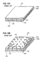
- Figs. 15A and 15B show an outline structure of the conventional BGA type semiconductor device.
- Fig. 15A is an oblique perspective view showing the front side of the BGA type semiconductor device.
- Fig. 15B is an oblique perspective view showing the back side of the BGA type semiconductor device.
- Fig. 16 shows a cross-sectional view of the BGA type semiconductor devices 101 separated in individual dies along a dicing line.
- a first wiring 107 is provided on an insulation film 108 formed on a front surface of the semiconductor substrate 104.
- the front surface of the semiconductor substrate 104 is attached on the first glass substrate 102 with the resin layer 105a.
- a back surface of the semiconductor die 104 is attached on the second glass substrate 103 with the resin layer 105b made of epoxy resin or the like.
- the first wiring 107 is connected to the second wiring 109.
- the second wiring 109 extends from the end of the first wiring 107 onto the surface of the second glass substrate 103.
- the ball-shaped conductive terminal 106 is formed on the second wiring 109 extended onto the second glass substrate 103.
- a protection film 110 made of a solder resist or the like is further formed on the surface of the second wiring 109. Relevant technologies are disclosed in Japanese Patent Application Publication No. 2002-512436 .
- the invention provides a method of manufacturing a semiconductor device including: attaching a supporting body on a front surface of a semiconductor substrate having a first and second pad electrode; forming an opening in the supporting body to expose at least partially the first pad electrode and the second pad electrode; and cutting the semiconductor substrate and the supporting body between the first and second pad electrode.
- an electronic device is formed on the front surface of the semiconductor substrate, and the supporting body in a region not overlapping the electronic device is preferably thinned by etching before forming the opening.
- the invention also provides a semiconductor device including: a semiconductor substrate having an electronic device and an external connection electrode electrically connected to the electronic device; and a supporting body attached on the semiconductor substrate over the electronic device; wherein an opening is provided on a periphery of the supporting body in a direction from outside to inside, and the external connection electrode is formed in the opening.
- the supporting body in a region overlapping the electronic device is preferably thicker than a portion of the supporting body in a region not overlapping the electronic device.
- the invention also provides a camera module including: an image pickup device; a circuit board having an external electrode and mounted with the image pickup device; and a lens leading light to a light receiving region of the image pickup device, the image pickup device including: a semiconductor substrate having a light receiving element and an external connection electrode electrically connected to the light receiving element; and a supporting body attached on the semiconductor substrate over the light receiving element and having an opening penetrating the body; wherein the external electrode of the circuit board and the external connection electrode are electrically connected through the opening.
- the opening is preferably formed on a periphery of the supporting body in a direction from outside to inside.
- the supporting body in a region overlapping the light receiving element is preferably thicker than a portion of the supporting body in a region not overlapping the light receiving element.
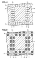
- FIG. 1A is a plan view of the upper side of a semiconductor device 200
- Fig. 1B is a cross-sectional view of Fig. 1A along line X-X.
- Openings 208 are formed in a predetermined region of the supporting body 204, penetrating the body 204 from its front surface to its back surface, and a plurality of conductive terminals 209 made of solder or the like is formed in the openings, 208 respectively.
- the conductive terminals 209 are electrically connected with the pad electrodes 202 with a metal layer 210 made of nickel or gold interposed therebetween.
- the conductive terminals 209 are directly formed in the plurality of openings 208 provided in the supporting body 204 respectively, there is no need to provide the wirings as shown in the conventional art, providing an advantage that the manufacturing process is simplified. Furthermore, since the front surface of the semiconductor substrate 203 is protected by the supporting body 204, the electronic devices 201 or the surrounding elements on the front surface are prevented from deteriorating, thereby enhancing the reliability and yield of the semiconductor device.
- a second embodiment of the invention is directed to simplification of a process of manufacturing a semiconductor device and enhancement of the reliability and yield of the semiconductor device.
- the invention is also directed to reduction of the size of a camera module set with a semiconductor device as an image pickup device and enhancement of its reliability and yield.
- FIG. 2B is a schematic plan view of the upper side of the semiconductor device of the embodiment.
- Figs. 3A to 5 are cross-sectional views of Fig. 2 along line Y-Y, being shown in manufacturing order.
- a semiconductor substrate 2 made of silicon (Si) or the like that is formed with an electronic device 1 on its front surface is prepared.
- a first insulation film 3 e.g. a silicon oxide film or a BPSG film formed by a thermal oxidation method, a CVD method, or the like
- a thickness of, for example, 2 ⁇ m is formed on a front surface of the semiconductor substrate 2 to have a thickness of, for example, 2 ⁇ m.
- a metal layer made of aluminum (Al), copper (Cu) or the like is formed by a sputtering method, a plating method, or the other deposition method, and then the metal layer is etched using a photoresist layer (not shown) as a mask to form a pad electrode 4 having a thickness of, for example, 1 ⁇ m on the first insulation film 3.
- the pad electrode 4 is electrically connected with the electronic device 1 or the surrounding elements.
- a passivation film 5 (e.g. a silicon nitride film formed by a CVD method) is formed on the front surface of the semiconductor substrate 2, covering a portion of the pad electrode 4.
- a photoresist layer 8 is selectively formed on a surface of the supporting body 7.
- the photoresist layer 8 is formed so as to have an opening in two conductive terminal formation regions 9 adjacent to each other over a dicing line DL and in a region between these regions 9.
- the supporting body 7 is selectively etched using the photoresist layer 8 as a mask.
- the supporting body 7 in the two conductive terminal formation regions 9 facing over the dicing line DL and the supporting body 7 in the region connecting with these regions 9. therebetween are removed as a unit, thereby forming an opening 10 penetrating the supporting body 7.
- the openings 10 are formed along the periphery of the supporting body 7 at equal intervals as shown in Fig. 2A, when seen from the upper side.
- This selective etching is, for example, dry-etching, or dip etching with hydrofluoride (HF) as an etching solution.
- HF hydrofluoride
- an etching unit of the supporting body covers two conductive terminal formation regions and covers the twice larger area, so that the opening is easily formed in a desired position with high accuracy.
- the resin layer 6 exposed at a bottom of the opening 10 is selectively etched to expose a portion of the pad electrode 4. It is noted that the supporting body 7 and the resin layer 6 may be etched at a time.
- a metal layer 11 made of nickel (Ni) and gold (Au) or the like is formed on the pad electrode 4 exposed at the bottom of the opening 10.
- a solder ball is bonded to a predetermined region of the metal layer 11 by an electrolytic plating method using the metal layer 11 as a plating electrode, thereby forming a conductive terminal 12.
- This conductive terminal 12 may be also formed by screen-printing solder and reflowing the solder by heat treatment.
- the method of forming the conductive terminal 12 is not limited to these, and may be also formed by a so-called dispensing (coating) method in which solder or the like is coated with a dispenser.
- the conductive terminal 12 may be made of gold, and its material is not particularly limited. Furthermore, there is also a case of not forming the conductive terminal 12 as described below. In this case, the metal layer 11 or the pad electrode 4 is exposed.
- Fig. 2B is a schematic plan view after the dicing.
- the semiconductor device of this embodiment is thus completed.
- the completed semiconductor device is mounted on a circuit board formed with an external electrode by patterning or the like.
- the conductive terminal 12 is electrically connected to the external electrode on the circuit board, serving as an external connection electrode.
- the metal layer 11 or the pad electrode 4 is electrically connected to the external electrode on the circuit board through a bonding wire or the like, serving as the external connection electrode.
- the second embodiment has an advantage that a complex wiring such as conventionally needed is not necessary and the manufacturing process is simplified. Furthermore, since the front surface of the semiconductor substrate 2 is protected by the supporting body 7, the electronic device 1 or the surrounding elements formed on the front surface are prevented from deteriorating, thereby enhancing the reliability of the semiconductor device. Furthermore, since the opening 10 is easily formed in the supporting body 7 as described above, the manufacturing cost is minimized, resulting in enhancement of the reliability and yield of the semiconductor device.
- the semiconductor device of the second embodiment is mounted on the circuit board (a module substrate) referring to figures.
- the electronic device 1 is used as a light receiving element such as a CCD image sensor or a CMOS image sensor
- the semiconductor die 15 is used as an image pickup device of a camera module.
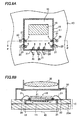
- Fig. 6A is a plan view of the upper side of a camera module mounted with the semiconductor device of this embodiment
- Fig. 6B is a cross-sectional view of Fig. 6A along line Z-Z.
- the semiconductor die 15 is mounted on a circuit board 1A such as, for example, a printed board.
- the semiconductor die 15 is so formed that its back surface side (the side not formed with the supporting body 7) faces the circuit board 1A.
- External electrodes 20 are formed on the circuit board 1A by patterning.
- the pad electrodes 4 of the semiconductor die 15 and the external electrodes 20 are electrically connected through, for example, bonding wires 21.
- a flexible sheet or tape formed with a conductive pattern may be used instead of the bonding wire 21.
- the metal layer 11 may be formed on the pad electrode 4 and this metal layer 11 and the external electrode 20 may be electrically connected through the bonding wire 21 or the like.
- a lens barrel 30 is provided on a front surface of the circuit board 1A, covering the semiconductor die 15.
- a filter 31 cutting light of a predetermined wavelength and a lens 32 focusing external light are provided in the lens barrel 30 in a position corresponding to the light receiving region 16 of the semiconductor die 15.
- the back surface of the semiconductor die 15 is not formed with a conductive terminal and is planarized, thereby minimizing slanting or shifting of the semiconductor die 15 when this is mounted. Furthermore, this prevents undesirable influence on an image when taken by the camera module.
- a DSP (digital signal processor) chip 40 processing an image signal sent from the light receiving element may be disposed on a back surface of the circuit board 1A.
- the semiconductor die 15 and the DSP chip 40 By superposingly forming the semiconductor die 15 and the DSP chip 40 on the front surface and the back surface of the circuit board 1A respectively, the area of the circuit board 1A is reduced.
- the semiconductor device of the embodiment may be mounted on the circuit board in a manner shown in Figs. 7A and 7B.
- Fig. 7A is a plan view of the upper side of the semiconductor device of this embodiment, which is mounted as an image pickup device of a camera module
- Fig. 7B is a cross-sectional view of Fig. 7A along line O-O.
- the same numerals are given to the same components as those shown in Figs. 6A and 6B and description thereof will be omitted.
- the semiconductor die 15 is so mounted that its front surface faces a back surface of a circuit board 1B such as, for example, a printed board.
- the conductive terminals 12 are directly connected to the external electrodes 20 formed on the back surface of the circuit board 1B by patterning.
- An opening is formed in the circuit board 1B in a region overlapping the light receiving region 16 to provide a light receiving window 1W. Therefore, the semiconductor die 15 receives light even when it is mounted on the back surface of the circuit board 1B.
- the thickness of the circuit board 1B forms a part of the focal length. Therefore, compared with the structure where the semiconductor die 15 is disposed above the circuit board as shown in Figs. 6A and 6B, the reduction of the height of the lens barrel 30 is achieved at least by an amount of a thickness H of the circuit board 1B, so that the size of the camera module is reduced.
- the filter 31 may be fixed on the circuit board 1B as shown by a dotted line in Fig. 7B using a special jig.
- the filter 31 not only as a filter that is its original role (cutting light of a predetermined wavelength) but also as a lid sealing the front surface of the semiconductor die 15, dusts and foreign substances are effectively prevented from being attached to the light receiving surface (the front surface of the supporting body 7) and thus the reliability of the camera module is enhanced.
- the semiconductor device of this embodiment may be mounted on the circuit board in a manner shown in Figs. 8A and 8B.
- Fig. 8A is a plan view of the upper side of a camera module mounted with the semiconductor device of this embodiment
- Fig. 8B is a cross-sectional view of Fig. 8A along line P-P.
- the same numerals are given to the same components as those shown in Figs. 6A, 6B, 7A, and 7B, and description thereof will be omitted.
- a concave portion H1 is formed in a circuit board 1C such as, for example, a printed board, and the semiconductor die 15 is disposed, being embedded in the concave portion H1.
- the concave portion H1 is formed by etching with laser irradiation or cutting with a drill, for example.
- a Cu layer 20m made of, for example, copper that has high heat conductivity is formed as a radiation layer on a bottom of the concave portion Hl, contacting the back surface of the semiconductor die 15. This structure allows heat generated during the operation of the semiconductor die 15 to escape from a bottom of the semiconductor die 15 to the Cu layer 20m and to the outside.
- the electronic device 1 is a light receiving element such as CCD that is easy to degrade in electric characteristics with heat, its performance is prevented from degrading and its operation quality is enhanced.
- an underfill 22 e.g. an organic material such as epoxy resin.
- the pad electrodes 4 and the external electrodes 20 of the circuit board 1C are connected through the bonding wires 21.
- the metal layer 11 may be formed on the pad electrode 4, and the metal layer 11 and the external electrode 20 may be electrically connected through the bonding wire 21 or the like.
- a wiring made of, for example, a conductive paste 21p containing silver (Ag) particles may be used instead of the bonding wire 21 as shown in Fig. 9.
- the conductive paste 21p is formed from the opening on the pad electrode 4 onto the external electrode 20.
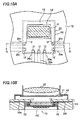
- the semiconductor device of this embodiment may be mounted on the circuit board in a manner shown in Figs. 10A and 10B.
- Fig. 10A is a plan view of the upper side of a camera module mounted with the semiconductor device of this embodiment
- Fig. 10B is a cross-sectional view of Fig. 10A along line Q-Q.
- the same numerals are given to the same components as those described above and description thereof will be omitted.
- a concave portion H2 is formed on a back surface side of a circuit board 1D such as a printed board, and the semiconductor die 15 is disposed, being embedded in the concave portion H2.
- the concave portion H2 is formed by etching with laser irradiation or cutting with a drill, for example.
- a Cu layer 20n is formed as a wiring layer for an external electrode in the circuit board 1D, for example, and electrically connected to the conductive terminal 12 that is an external connection electrode.
- the light receiving window 1W is provided in the circuit board 1D in a region corresponding to the light receiving region 16. Therefore, the semiconductor die 15 receives light even when it is mounted on the back surface of the circuit board 1D.
- the thickness of the circuit board 1D forms a part of the focal length. Therefore, compared with the structure where the semiconductor die 15 is disposed above the circuit board as shown in Figs. 8A and 8B, the reduction of the height of the lens barrel 30 is achieved, so that the size of the camera module is reduced.
- the space is filled with the underfill 22.
- FIGS. 11A to 13 are cross-sectional views shown in manufacturing order. The same numerals are given to the same components as those described above and description thereof will be omitted.
- the semiconductor substrate 2 made of silicon (Si) or the like that is formed with the electronic device 1 on its front surface is prepared as shown in Fig. 11A. Then, the first insulation film 3 is formed on the front surface of the semiconductor substrate 2.
- a metal layer made of aluminum (Al), copper (Cu), or the like is formed by a sputtering method, a plating method, or the other deposition method, and the metal layer is etched using a photoresist layer (not shown) as a mask to form the pad electrode 4 on the first insulation film 3.
- the passivation film 5 is formed on the front surface of the semiconductor substrate 2, covering a portion of the pad electrode 4.
- the supporting body 7 is attached on the front surface of the semiconductor substrate 2 including on the pad electrode 4 with the resin layer 6 made of epoxy resin or the like interposed therebetween. Then, according to needs, back-grinding is performed to the back surface of the semiconductor substrate 2 to thin the semiconductor substrate 2.
- a photoresist layer 50 is selectively formed on the front surface of the supporting body 7.
- the photoresist layer 50 is formed at least in a region overlapping the electronic device 1, or more preferably only in a region overlapping the electronic device 1.
- the supporting body 7 is selectively etched using the photoresist layer 50 as a mask. By this etching, the supporting body 7 in a predetermined region (a portion thereof in a region not overlapping the electronic device) is etched and thinned by a predetermined amount. For example, the supporting body 7 having a thickness about 100 ⁇ m is thinned to about 30 ⁇ m in this region.
- a photoresist layer 55 is selectively formed on the front surface of the supporting body 7.
- the supporting body 7 is selectively etched using the photoresist layer 55 as a mask.
- the supporting body 7 in two conductive terminal formation regions 9 facing over the dicing line DL and the supporting body 7 in a region connecting with these regions 9 therebetween are removed at the same time, thereby forming the opening 10 penetrating the supporting body 7.
- the supporting body 7 is formed to have a convex shape, and the supporting body 7 in the region overlapping the electronic device 1 is thicker than in the other region.
- the resin layer 6 exposed at the bottom of the opening 10 is selectively etched to expose a portion of the pad electrode 4.
- the metal layer 11 made of nickel (Ni) and gold (Au) or the like is formed on the pad electrode 4 exposed at the bottom of the opening 10.
- the conductive terminal 12 is formed in a predetermined region of the metal layer 11. Although not shown in the figures, there is also a case of not forming the conductive terminal 12 like in the second embodiment. Lastly, as shown in Fig. 13, the semiconductor substrate 2 is separated in individual semiconductor dies 60 along the dicing line DL. The semiconductor device of the third embodiment is thus completed.
- the third embodiment also has an advantage that a complex wiring such as conventionally needed is not necessary and the manufacturing process is simplified. Furthermore, the front surface of the semiconductor substrate 2 is protected by the supporting body 7 and the electronic device 1 or the surrounding elements formed on the front surface are prevented from deteriorating, thereby enhancing the reliability of the semiconductor device. Furthermore, since the opening 10 is easily formed in the supporting body 7 in the similar manner to the second embodiment, the manufacturing cost is reduced and the reliability and yield of the semiconductor device are enhanced.
- the electronic device 1 is a light receiving element such as a CCD image sensor, a CMOS image sensor, or the like.
- Fig. 14A is a plan view of the upper side of a camera module mounted with the semiconductor device of the third embodiment
- Fig. 14B is a cross-sectional view of Fig. 14A along line R-R.
- the semiconductor die 60 is so mounted that its front surface faces a back surface of a circuit board 1E such as, for example, a printed board.
- the conductive terminals 12 are directly connected with the external electrodes 20 formed on the back surface of the circuit board 1E by patterning.
- an opening is formed in the circuit board 1E in a region overlapping the light receiving region 16 to provide the light receiving window 1W. Therefore, the semiconductor die 60 receives light even when it is mounted on the back surface of the circuit board 1E.
- the thicker portion of the supporting body 7 (the convex portion) is fitted in the light receiving window 1W of the circuit board 1E with an adhesive (not shown). Therefore, only the front surface of the thicker portion of the supporting body 7 is exposed from the light receiving window 1W.
- This structure of the semiconductor die where the supporting body 7 in a predetermined region is formed thicker facilitates cleaning of the front surface of the supporting body 7 in the light receiving region 16 after the die is mounted on the camera module, in addition to the effect of the semiconductor device of the second embodiment.
- the workability of the cleaning is further enhanced by making the height positions of the front surfaces of the supporting body 7 and the circuit board 1E almost the same. This further prevents the adhesive used for mounting the semiconductor die from reaching the front surface of the supporting body 7 in the light receiving region 16. Therefore, this structure has an advantage that the maintainability and reliability of the camera module are enhanced.
- a predetermined cleaning tool such as a swab.
- the thickness of the circuit board 1E forms a part of the focal length. Therefore, compared with the structure where the semiconductor die 15 is disposed above the circuit board as shown in Figs. 6A and 6B, the reduction of the height of the lens barrel 30 is achieved at least by an amount of a thickness H3 of the circuit board 1E, so that the size of the camera module is reduced.
- the third embodiment is the same as the second embodiment in that dusts and foreign substances are effectively prevented from being attached to the light receiving surface (the front surface of the supporting body 7) and the reliability of the camera module is enhanced by disposing the filter 31 in a manner shown by a dotted line in Fig. 14B and using the filter 31 as a lid sealing the front surface of the semiconductor die 60.
- the third embodiment is also the same as the second embodiment in that the semiconductor die 60 is mounted on the circuit board in the various manners.
- the electronic devices or the surrounding elements on the front surface are prevented from deteriorating, thereby enhancing the reliability and yield of the semiconductor device.
- the manufacturing cost is minimized and the reliability and yield of the semiconductor device are enhanced.
- the size of the camera module of the invention is reduced and its reliability is enhanced.
Landscapes
- Engineering & Computer Science (AREA)
- Multimedia (AREA)
- Signal Processing (AREA)
- Solid State Image Pick-Up Elements (AREA)
- Dicing (AREA)
- Transforming Light Signals Into Electric Signals (AREA)
- Studio Devices (AREA)
- Lens Barrels (AREA)
Abstract
Description
- The invention relates to a semiconductor device, particularly, a package type semiconductor device and a method of manufacturing the same. The invention also relates to a camera module having a package type semiconductor device.
- A CSP (chip size package) has received attention in recent years as a new packaging technology. The CSP is a small package having about the same outside dimensions as those of a semiconductor die packaged in it.
- A BGA (ball grid array) type semiconductor device has been known as a type of the CSP. In the BGA type semiconductor device, a plurality of ball-shaped conductive terminals made of metal such as solder is arrayed on one surface of a package and is electrically connected to a semiconductor die mounted on the other surface of the package.
- When the BGA type semiconductor device is mounted on electronic equipment, the semiconductor die is electrically connected to an external circuit on a printed board by bonding the conductive terminals to wiring patterns on the printed board.
- Such a BGA type semiconductor device has advantages in providing a large number of conductive terminals and in reducing a size over the other CSP type semiconductor devices such as an SOP (small outline package) and a QFP (quad flat Package), which have lead pins protruding from their sides. Therefore, the BGA type semiconductor device has a wide field of application, for example, as an image sensor chip of a digital camera mounted on acellular phone or the like.
- Figs. 15A and 15B show an outline structure of the conventional BGA type semiconductor device. Fig. 15A is an oblique perspective view showing the front side of the BGA type semiconductor device. Fig. 15B is an oblique perspective view showing the back side of the BGA type semiconductor device.
- A
semiconductor substrate 104 is sealed between afirst glass substrate 102 and asecond glass substrate 103 withresin layers type semiconductor device 101. A plurality ofconductive terminals 106 is arrayed in a grid pattern on a surface of thesecond glass substrate 103, that is, on a back surface of the BGAtype semiconductor device 101. Theconductive terminals 106 are connected to thesemiconductor substrate 104 throughsecond wirings 109. The plurality ofsecond wirings 109 is connected with aluminum wirings extending from inside thesemiconductor substrate 104, making each of theconductive terminals 106 electrically connected with thesemiconductor die 104. - More detailed explanation on a cross-sectional structure of the BGA
type semiconductor device 101 will be given hereafter referring to Fig. 16. Fig. 16 shows a cross-sectional view of the BGAtype semiconductor devices 101 separated in individual dies along a dicing line. - A
first wiring 107 is provided on aninsulation film 108 formed on a front surface of thesemiconductor substrate 104. The front surface of thesemiconductor substrate 104 is attached on thefirst glass substrate 102 with theresin layer 105a. A back surface of thesemiconductor die 104 is attached on thesecond glass substrate 103 with theresin layer 105b made of epoxy resin or the like. - One end of the
first wiring 107 is connected to thesecond wiring 109. Thesecond wiring 109 extends from the end of thefirst wiring 107 onto the surface of thesecond glass substrate 103. The ball-shapedconductive terminal 106 is formed on thesecond wiring 109 extended onto thesecond glass substrate 103. - A
protection film 110 made of a solder resist or the like is further formed on the surface of thesecond wiring 109. Relevant technologies are disclosed inJapanese Patent Application Publication No. 2002-512436 - However, there is a problem that a process of manufacturing the described
conventional semiconductor device 101 is complex. Furthermore, the reliability of the describedsemiconductor device 101 is not enough because of its complex structure. For example, there is a possibility that thefirst wiring 107 and thesecond wiring 109 of the BGAtype semiconductor device 101 are disconnected at a point of contact between them since the area of the point of contact is very small. There is also a problem of insufficient step coverage of thesecond wiring 109. It is thus an object of the invention to provide an improved semiconductor device and manufacturing method thereof. - The solution according to the invention resides in the features of the independent claims and preferably in those of the dependent claims.
- Features of the invention are as follows. That is, the invention provides a method of manufacturing a semiconductor device including: attaching a supporting body on a front surface of a semiconductor substrate having a first and second pad electrode; forming an opening in the supporting body to expose at least partially the first pad electrode and the second pad electrode; and cutting the semiconductor substrate and the supporting body between the first and second pad electrode.
- In the method of the invention, an electronic device is formed on the front surface of the semiconductor substrate, and the supporting body in a region not overlapping the electronic device is preferably thinned by etching before forming the opening.
- The invention also provides a semiconductor device including: a semiconductor substrate having an electronic device and an external connection electrode electrically connected to the electronic device; and a supporting body attached on the semiconductor substrate over the electronic device; wherein an opening is provided on a periphery of the supporting body in a direction from outside to inside, and the external connection electrode is formed in the opening.
- In the semiconductor device of the invention, the supporting body in a region overlapping the electronic device is preferably thicker than a portion of the supporting body in a region not overlapping the electronic device.
- The invention also provides a camera module including: an image pickup device; a circuit board having an external electrode and mounted with the image pickup device; and a lens leading light to a light receiving region of the image pickup device, the image pickup device including: a semiconductor substrate having a light receiving element and an external connection electrode electrically connected to the light receiving element; and a supporting body attached on the semiconductor substrate over the light receiving element and having an opening penetrating the body; wherein the external electrode of the circuit board and the external connection electrode are electrically connected through the opening.
- In the camera module of the invention, the opening is preferably formed on a periphery of the supporting body in a direction from outside to inside.
- In the camera module of the invention, the supporting body in a region overlapping the light receiving element is preferably thicker than a portion of the supporting body in a region not overlapping the light receiving element.
-
- Figs. 1A and 1B are respectively a plan view and a cross-sectional view for explaining a semiconductor device and its manufacturing method of a first embodiment the invention.
- Fig. 2A and 2B is a plan view for explaining a semiconductor device and its manufacturing method of a second embodiment of the invention.
- Figs. 3A to 5 are cross-sectional views for explaining the semiconductor device and its manufacturing method of the second embodiment of the invention.
- Figs. 6A and 6B are respectively a plan view and a cross-sectional view for explaining a state where the semiconductor device of the second embodiment of the invention is mounted.
- Figs. 7A and 7B are respectively a plan view and a cross-sectional view for explaining a state where the semiconductor device of the second embodiment of the invention is mounted.
- Figs. 8A and 8B are respectively a plan view and a cross-sectional view for explaining a state where the semiconductor device of the second embodiment of the invention is mounted.
- Fig. 9 is a cross-sectional view for explaining a state where the semiconductor device of the second embodiment of the invention is mounted.
- Figs. 10A and 10B are respectively a plan view and a cross-sectional view for explaining a state where the semiconductor device of the second embodiment of the invention is mounted.
- Figs. 11A to 13 are cross-sectional views for explaining a semiconductor device and its manufacturing method of a third embodiment of the invention.
- Figs. 14A and 14B are respectively a plan view and a cross-sectional view for explaining a state where the semiconductor device of the third embodiment of the invention is mounted.
- Figs. 15A and 15B are perspective views for explaining a conventional semiconductor device.
- Fig. 16 is a cross-sectional view for explaining the conventional semiconductor device.
- A first embodiment of this invention is directed to solving the problems identified above and shown in Figs. 1A and 1B. Fig. 1A is a plan view of the upper side of a
semiconductor device 200, and Fig. 1B is a cross-sectional view of Fig. 1A along line X-X. - In the
semiconductor device 200, a supportingbody 204 made of glass is attached on asemiconductor substrate 203 formed withelectronic devices 201 andpad electrodes 202 on its front surface with aresin layer 205 interposed therebetween. A numeral 206 designates an insulation film made of a BPSG or silicon oxide film, and a numeral 207 designates a passivation film made of a silicon nitride film or the like and covering a portion of thepad electrode 202. -
Openings 208 are formed in a predetermined region of the supportingbody 204, penetrating thebody 204 from its front surface to its back surface, and a plurality ofconductive terminals 209 made of solder or the like is formed in the openings, 208 respectively. Theconductive terminals 209 are electrically connected with thepad electrodes 202 with ametal layer 210 made of nickel or gold interposed therebetween. - In this structure, since the
conductive terminals 209 are directly formed in the plurality ofopenings 208 provided in the supportingbody 204 respectively, there is no need to provide the wirings as shown in the conventional art, providing an advantage that the manufacturing process is simplified. Furthermore, since the front surface of thesemiconductor substrate 203 is protected by the supportingbody 204, theelectronic devices 201 or the surrounding elements on the front surface are prevented from deteriorating, thereby enhancing the reliability and yield of the semiconductor device. - However, since each of the
openings 208 in thissemiconductor device 200 is micro-sized (e.g. forms an almost square shape of about 100×100µm), there is a problem of difficulty in formation of theopenings 208 with desired size in target positions of the supportingbody 204 with high accuracy. - Thus, a second embodiment of the invention is directed to simplification of a process of manufacturing a semiconductor device and enhancement of the reliability and yield of the semiconductor device. The invention is also directed to reduction of the size of a camera module set with a semiconductor device as an image pickup device and enhancement of its reliability and yield.
- A semiconductor device and a method of manufacturing the semiconductor device of the second embodiment of the invention will be described referring to figures. Fig. 2B is a schematic plan view of the upper side of the semiconductor device of the embodiment. Figs. 3A to 5 are cross-sectional views of Fig. 2 along line Y-Y, being shown in manufacturing order.
- One of features of the semiconductor device of the second embodiment of the invention is that a plurality of
openings 10 is provided along a periphery of a supportingbody 7 in a direction from outside to inside as shown in Fig. 2B, and aconductive terminal 12 and ametal layer 11 that are to be electrically connected to the other circuit board are formed in each of theopenings 10. Hereafter, the method of manufacturing the semiconductor device will be described in detail. - First, as shown in Fig. 3A, a
semiconductor substrate 2 made of silicon (Si) or the like that is formed with anelectronic device 1 on its front surface is prepared. Then, a first insulation film 3 (e.g. a silicon oxide film or a BPSG film formed by a thermal oxidation method, a CVD method, or the like) is formed on a front surface of thesemiconductor substrate 2 to have a thickness of, for example, 2µm. - Then, a metal layer made of aluminum (Al), copper (Cu) or the like is formed by a sputtering method, a plating method, or the other deposition method, and then the metal layer is etched using a photoresist layer (not shown) as a mask to form a
pad electrode 4 having a thickness of, for example, 1µm on thefirst insulation film 3. Thepad electrode 4 is electrically connected with theelectronic device 1 or the surrounding elements. - Then, a passivation film 5 (e.g. a silicon nitride film formed by a CVD method) is formed on the front surface of the
semiconductor substrate 2, covering a portion of thepad electrode 4. - Then, a supporting
body 7 is attached on the front surface of thesemiconductor substrate 2 including on thepad electrode 4 with aresin layer 6 made of epoxy resin or the like interposed therebetween. The supportingbody 7 is made of, for example, glass, quartz, plastic, or the like, and has a function of supporting thesemiconductor substrate 2 and protecting the front surface thereof. When theelectronic device 1 is a light receiving element such as CCD, the supportingbody 7 is made of a transparent or semitransparent material and has light transmission characteristics. Then, according to needs, back-grinding is performed to a back surface of thesemiconductor substrate 2 to thin thesemiconductor substrate 2. - Next, as shown in Fig. 3B, a
photoresist layer 8 is selectively formed on a surface of the supportingbody 7. Thephotoresist layer 8 is formed so as to have an opening in two conductiveterminal formation regions 9 adjacent to each other over a dicing line DL and in a region between theseregions 9. - Next, as shown in Fig. 3C, the supporting
body 7 is selectively etched using thephotoresist layer 8 as a mask. By this etching, the supportingbody 7 in the two conductiveterminal formation regions 9 facing over the dicing line DL and the supportingbody 7 in the region connecting with theseregions 9. therebetween are removed as a unit, thereby forming anopening 10 penetrating the supportingbody 7. Theopenings 10 are formed along the periphery of the supportingbody 7 at equal intervals as shown in Fig. 2A, when seen from the upper side. - This selective etching is, for example, dry-etching, or dip etching with hydrofluoride (HF) as an etching solution. Compared with a semiconductor device 200 (see Fig. 1A) where an etching unit is each conductive terminal formation region, an etching unit of the supporting body covers two conductive terminal formation regions and covers the twice larger area, so that the opening is easily formed in a desired position with high accuracy.
- Next, as shown in Fig. 4A, the
resin layer 6 exposed at a bottom of theopening 10 is selectively etched to expose a portion of thepad electrode 4. It is noted that the supportingbody 7 and theresin layer 6 may be etched at a time. - Next, as shown in Fig. 4B, a
metal layer 11 made of nickel (Ni) and gold (Au) or the like is formed on thepad electrode 4 exposed at the bottom of theopening 10. - Next, as shown in Fig. 4C, a solder ball is bonded to a predetermined region of the
metal layer 11 by an electrolytic plating method using themetal layer 11 as a plating electrode, thereby forming aconductive terminal 12. This conductive terminal 12 may be also formed by screen-printing solder and reflowing the solder by heat treatment. The method of forming theconductive terminal 12 is not limited to these, and may be also formed by a so-called dispensing (coating) method in which solder or the like is coated with a dispenser. Theconductive terminal 12 may be made of gold, and its material is not particularly limited. Furthermore, there is also a case of not forming theconductive terminal 12 as described below. In this case, themetal layer 11 or thepad electrode 4 is exposed. - Lastly, as shown in Fig. 5, the
semiconductor substrate 2 is separated in individual semiconductor dies 15 along the dicing line DL. Fig. 2B is a schematic plan view after the dicing. The semiconductor device of this embodiment is thus completed. The completed semiconductor device is mounted on a circuit board formed with an external electrode by patterning or the like. In this mounting process, theconductive terminal 12 is electrically connected to the external electrode on the circuit board, serving as an external connection electrode. In the case of not forming theconductive terminal 12, themetal layer 11 or thepad electrode 4 is electrically connected to the external electrode on the circuit board through a bonding wire or the like, serving as the external connection electrode. - The second embodiment has an advantage that a complex wiring such as conventionally needed is not necessary and the manufacturing process is simplified. Furthermore, since the front surface of the
semiconductor substrate 2 is protected by the supportingbody 7, theelectronic device 1 or the surrounding elements formed on the front surface are prevented from deteriorating, thereby enhancing the reliability of the semiconductor device. Furthermore, since theopening 10 is easily formed in the supportingbody 7 as described above, the manufacturing cost is minimized, resulting in enhancement of the reliability and yield of the semiconductor device. - Next, descriptions will be given on a case where the semiconductor device of the second embodiment is mounted on the circuit board (a module substrate) referring to figures. In the following description, the
electronic device 1 is used as a light receiving element such as a CCD image sensor or a CMOS image sensor, and the semiconductor die 15 is used as an image pickup device of a camera module. Fig. 6A is a plan view of the upper side of a camera module mounted with the semiconductor device of this embodiment, and Fig. 6B is a cross-sectional view of Fig. 6A along line Z-Z. - As shown in Fig. 6A, the semiconductor die 15 is mounted on a circuit board 1A such as, for example, a printed board. The semiconductor die 15 is so formed that its back surface side (the side not formed with the supporting body 7) faces the circuit board 1A.
External electrodes 20 are formed on the circuit board 1A by patterning. - Then, the
pad electrodes 4 of the semiconductor die 15 and theexternal electrodes 20 are electrically connected through, for example,bonding wires 21. A flexible sheet or tape formed with a conductive pattern may be used instead of thebonding wire 21. Although not shown in the figures, themetal layer 11 may be formed on thepad electrode 4 and thismetal layer 11 and theexternal electrode 20 may be electrically connected through thebonding wire 21 or the like. - Furthermore, as shown in Fig. 6B, a
lens barrel 30 is provided on a front surface of the circuit board 1A, covering the semiconductor die 15. Afilter 31 cutting light of a predetermined wavelength and alens 32 focusing external light are provided in thelens barrel 30 in a position corresponding to thelight receiving region 16 of the semiconductor die 15. Differing from a conventional semiconductor device 101 (see Fig. 15), the back surface of the semiconductor die 15 is not formed with a conductive terminal and is planarized, thereby minimizing slanting or shifting of the semiconductor die 15 when this is mounted. Furthermore, this prevents undesirable influence on an image when taken by the camera module. - A DSP (digital signal processor)
chip 40 processing an image signal sent from the light receiving element may be disposed on a back surface of the circuit board 1A. By superposingly forming the semiconductor die 15 and theDSP chip 40 on the front surface and the back surface of the circuit board 1A respectively, the area of the circuit board 1A is reduced. - Alternatively, the semiconductor device of the embodiment may be mounted on the circuit board in a manner shown in Figs. 7A and 7B. Fig. 7A is a plan view of the upper side of the semiconductor device of this embodiment, which is mounted as an image pickup device of a camera module, and Fig. 7B is a cross-sectional view of Fig. 7A along line O-O. The same numerals are given to the same components as those shown in Figs. 6A and 6B and description thereof will be omitted.
- As shown in Fig. 7A, the semiconductor die 15 is so mounted that its front surface faces a back surface of a
circuit board 1B such as, for example, a printed board. Theconductive terminals 12 are directly connected to theexternal electrodes 20 formed on the back surface of thecircuit board 1B by patterning. - An opening is formed in the
circuit board 1B in a region overlapping thelight receiving region 16 to provide alight receiving window 1W. Therefore, the semiconductor die 15 receives light even when it is mounted on the back surface of thecircuit board 1B. - Furthermore, since the semiconductor die 15 is mounted on the back surface of the
circuit board 1B in this structure, the thickness of thecircuit board 1B forms a part of the focal length. Therefore, compared with the structure where the semiconductor die 15 is disposed above the circuit board as shown in Figs. 6A and 6B, the reduction of the height of thelens barrel 30 is achieved at least by an amount of a thickness H of thecircuit board 1B, so that the size of the camera module is reduced. - By the way, when dusts and foreign substances are attached to a light receiving surface of the image pickup device in the camera module, its quality may be degraded by reduction of a light receiving amount or a blur occurring in an image. Therefore, the
filter 31 may be fixed on thecircuit board 1B as shown by a dotted line in Fig. 7B using a special jig. By using thefilter 31 not only as a filter that is its original role (cutting light of a predetermined wavelength) but also as a lid sealing the front surface of the semiconductor die 15, dusts and foreign substances are effectively prevented from being attached to the light receiving surface (the front surface of the supporting body 7) and thus the reliability of the camera module is enhanced. - Alternatively, the semiconductor device of this embodiment may be mounted on the circuit board in a manner shown in Figs. 8A and 8B. Fig. 8A is a plan view of the upper side of a camera module mounted with the semiconductor device of this embodiment, and Fig. 8B is a cross-sectional view of Fig. 8A along line P-P. The same numerals are given to the same components as those shown in Figs. 6A, 6B, 7A, and 7B, and description thereof will be omitted.
- As shown in Fig. 8B, a concave portion H1 is formed in a
circuit board 1C such as, for example, a printed board, and the semiconductor die 15 is disposed, being embedded in the concave portion H1. The concave portion H1 is formed by etching with laser irradiation or cutting with a drill, for example. - A
Cu layer 20m made of, for example, copper that has high heat conductivity is formed as a radiation layer on a bottom of the concave portion Hl, contacting the back surface of the semiconductor die 15. This structure allows heat generated during the operation of the semiconductor die 15 to escape from a bottom of the semiconductor die 15 to theCu layer 20m and to the outside. - This effectively prevents degradation of the performance of the
electronic device 1 due to heat. Therefore, when theelectronic device 1 is a light receiving element such as CCD that is easy to degrade in electric characteristics with heat, its performance is prevented from degrading and its operation quality is enhanced. - Although the front surface of the
Cu layer 20m contacts the back surface of the semiconductor die 15 in Fig. 8B, these may not necessarily contact each other directly and an insulation film such as a silicon oxide film, a silicon nitride film, or a resin film may be formed therebetween. - When there is a space between a sidewall of the concave portion H1 and the semiconductor die 15 when the semiconductor die 15 is mounted, the space is filled with an underfill 22 (e.g. an organic material such as epoxy resin).
- Then, the
pad electrodes 4 and theexternal electrodes 20 of thecircuit board 1C are connected through thebonding wires 21. Although not shown in the figures, themetal layer 11 may be formed on thepad electrode 4, and themetal layer 11 and theexternal electrode 20 may be electrically connected through thebonding wire 21 or the like. Furthermore, a wiring made of, for example, aconductive paste 21p containing silver (Ag) particles may be used instead of thebonding wire 21 as shown in Fig. 9. Theconductive paste 21p is formed from the opening on thepad electrode 4 onto theexternal electrode 20. - Alternatively, the semiconductor device of this embodiment may be mounted on the circuit board in a manner shown in Figs. 10A and 10B. Fig. 10A is a plan view of the upper side of a camera module mounted with the semiconductor device of this embodiment, and Fig. 10B is a cross-sectional view of Fig. 10A along line Q-Q. The same numerals are given to the same components as those described above and description thereof will be omitted.
- As shown in Fig. 10B, a concave portion H2 is formed on a back surface side of a
circuit board 1D such as a printed board, and the semiconductor die 15 is disposed, being embedded in the concave portion H2. The concave portion H2 is formed by etching with laser irradiation or cutting with a drill, for example. - A
Cu layer 20n is formed as a wiring layer for an external electrode in thecircuit board 1D, for example, and electrically connected to theconductive terminal 12 that is an external connection electrode. Thelight receiving window 1W is provided in thecircuit board 1D in a region corresponding to thelight receiving region 16. Therefore, the semiconductor die 15 receives light even when it is mounted on the back surface of thecircuit board 1D. - Since the semiconductor die 15 is mounted on the back surface of the
circuit board 1D in this structure, the thickness of thecircuit board 1D forms a part of the focal length. Therefore, compared with the structure where the semiconductor die 15 is disposed above the circuit board as shown in Figs. 8A and 8B, the reduction of the height of thelens barrel 30 is achieved, so that the size of the camera module is reduced. - When there is a space between a sidewall of the concave portion H2 and the semiconductor die 15 when the semiconductor die 15 is mounted, the space is filled with the
underfill 22. - Next, a semiconductor device and a method of manufacturing the semiconductor device of a third embodiment of the invention will be described referring to figures. Hereafter, the method of manufacturing the semiconductor device will be described. Figs. 11A to 13 are cross-sectional views shown in manufacturing order. The same numerals are given to the same components as those described above and description thereof will be omitted.
- First, the
semiconductor substrate 2 made of silicon (Si) or the like that is formed with theelectronic device 1 on its front surface is prepared as shown in Fig. 11A. Then, thefirst insulation film 3 is formed on the front surface of thesemiconductor substrate 2. - Then, a metal layer made of aluminum (Al), copper (Cu), or the like is formed by a sputtering method, a plating method, or the other deposition method, and the metal layer is etched using a photoresist layer (not shown) as a mask to form the
pad electrode 4 on thefirst insulation film 3. - Then, the
passivation film 5 is formed on the front surface of thesemiconductor substrate 2, covering a portion of thepad electrode 4. Then, the supportingbody 7 is attached on the front surface of thesemiconductor substrate 2 including on thepad electrode 4 with theresin layer 6 made of epoxy resin or the like interposed therebetween. Then, according to needs, back-grinding is performed to the back surface of thesemiconductor substrate 2 to thin thesemiconductor substrate 2. - Next, as shown in Fig. 11B, a
photoresist layer 50 is selectively formed on the front surface of the supportingbody 7. Thephotoresist layer 50 is formed at least in a region overlapping theelectronic device 1, or more preferably only in a region overlapping theelectronic device 1. Then, the supportingbody 7 is selectively etched using thephotoresist layer 50 as a mask. By this etching, the supportingbody 7 in a predetermined region (a portion thereof in a region not overlapping the electronic device) is etched and thinned by a predetermined amount. For example, the supportingbody 7 having a thickness about 100µm is thinned to about 30µm in this region. - Next, as shown in Fig. 11C, a
photoresist layer 55 is selectively formed on the front surface of the supportingbody 7. Then, the supportingbody 7 is selectively etched using thephotoresist layer 55 as a mask. By this etching, the supportingbody 7 in two conductiveterminal formation regions 9 facing over the dicing line DL and the supportingbody 7 in a region connecting with theseregions 9 therebetween are removed at the same time, thereby forming theopening 10 penetrating the supportingbody 7. The supportingbody 7 is formed to have a convex shape, and the supportingbody 7 in the region overlapping theelectronic device 1 is thicker than in the other region. - Next, as shown in Fig. 12A, the
resin layer 6 exposed at the bottom of theopening 10 is selectively etched to expose a portion of thepad electrode 4. Then, as shown in Fig. 12B, themetal layer 11 made of nickel (Ni) and gold (Au) or the like is formed on thepad electrode 4 exposed at the bottom of theopening 10. - Next, as shown in Fig. 12C, the
conductive terminal 12 is formed in a predetermined region of themetal layer 11. Although not shown in the figures, there is also a case of not forming theconductive terminal 12 like in the second embodiment. Lastly, as shown in Fig. 13, thesemiconductor substrate 2 is separated in individual semiconductor dies 60 along the dicing line DL. The semiconductor device of the third embodiment is thus completed. - The third embodiment also has an advantage that a complex wiring such as conventionally needed is not necessary and the manufacturing process is simplified. Furthermore, the front surface of the
semiconductor substrate 2 is protected by the supportingbody 7 and theelectronic device 1 or the surrounding elements formed on the front surface are prevented from deteriorating, thereby enhancing the reliability of the semiconductor device. Furthermore, since theopening 10 is easily formed in the supportingbody 7 in the similar manner to the second embodiment, the manufacturing cost is reduced and the reliability and yield of the semiconductor device are enhanced. - Next, descriptions will be given on a case where the semiconductor device of the third embodiment is mounted on the circuit board referring to figures. In the following description, the
electronic device 1 is a light receiving element such as a CCD image sensor, a CMOS image sensor, or the like. Fig. 14A is a plan view of the upper side of a camera module mounted with the semiconductor device of the third embodiment, and Fig. 14B is a cross-sectional view of Fig. 14A along line R-R. - As shown in Fig. 14A, the semiconductor die 60 is so mounted that its front surface faces a back surface of a
circuit board 1E such as, for example, a printed board. Theconductive terminals 12 are directly connected with theexternal electrodes 20 formed on the back surface of thecircuit board 1E by patterning. - Furthermore, an opening is formed in the
circuit board 1E in a region overlapping thelight receiving region 16 to provide thelight receiving window 1W. Therefore, the semiconductor die 60 receives light even when it is mounted on the back surface of thecircuit board 1E. In this embodiment, the thicker portion of the supporting body 7 (the convex portion) is fitted in thelight receiving window 1W of thecircuit board 1E with an adhesive (not shown). Therefore, only the front surface of the thicker portion of the supportingbody 7 is exposed from thelight receiving window 1W. - This structure of the semiconductor die where the supporting
body 7 in a predetermined region is formed thicker facilitates cleaning of the front surface of the supportingbody 7 in thelight receiving region 16 after the die is mounted on the camera module, in addition to the effect of the semiconductor device of the second embodiment. The workability of the cleaning is further enhanced by making the height positions of the front surfaces of the supportingbody 7 and thecircuit board 1E almost the same. This further prevents the adhesive used for mounting the semiconductor die from reaching the front surface of the supportingbody 7 in thelight receiving region 16. Therefore, this structure has an advantage that the maintainability and reliability of the camera module are enhanced. As an example of the cleaning method, in detail, after thelens barrel 30 is dismounted, the front surface of the supportingbody 7 is cleaned with a predetermined cleaning tool such as a swab. - In this structure, since the semiconductor die 60 is mounted on the back surface of the
circuit board 1E, the thickness of thecircuit board 1E forms a part of the focal length. Therefore, compared with the structure where the semiconductor die 15 is disposed above the circuit board as shown in Figs. 6A and 6B, the reduction of the height of thelens barrel 30 is achieved at least by an amount of a thickness H3 of thecircuit board 1E, so that the size of the camera module is reduced. The third embodiment is the same as the second embodiment in that dusts and foreign substances are effectively prevented from being attached to the light receiving surface (the front surface of the supporting body 7) and the reliability of the camera module is enhanced by disposing thefilter 31 in a manner shown by a dotted line in Fig. 14B and using thefilter 31 as a lid sealing the front surface of the semiconductor die 60. The third embodiment is also the same as the second embodiment in that the semiconductor die 60 is mounted on the circuit board in the various manners. - In the embodiments, since the front surface of the semiconductor substrate is protected by the supporting body, the electronic devices or the surrounding elements on the front surface are prevented from deteriorating, thereby enhancing the reliability and yield of the semiconductor device.
- Furthermore, since the formation of the opening in the supporting body is easy, the manufacturing cost is minimized and the reliability and yield of the semiconductor device are enhanced. Furthermore, the size of the camera module of the invention is reduced and its reliability is enhanced.
Claims (13)
- A method of manufacturing a semiconductor device, comprising:providing a semiconductor substrate (2,203) comprising a first pad electrode (4, 202) and a second pad electrode (4, 202) formed on a front surface thereof;attaching a supporting body (7, 204) to the front surface of the semiconductor substrate(2, 203);forming an opening (10, 208) in the supporting body (7, 204) to expose at least partially the first pad electrode (4, 202) and the second pad electrode (4, 202); andcutting the semiconductor substrate (2, 203) and the supporting body (7, 204) attached to the semiconductor substrate (2, 203) between the first pad electrode (4, 202) and the second pad electrode (4, 202).
- The method of claim 1, further comprising forming a first metal layer (11, 210) on the exposed first pad electrode (4, 202) and a second metal layer (11, 210) on the exposed second pad electrode (4, 202) and forming a first conductive terminal (12, 209) on the first metal layer (11, 210) and a second conductive terminal (12, 209) on the second metal layer (11, 210).
- The method of claim 1 or 2, wherein the semiconductor substrate (2, 203) comprises an electronic device (1, 201) formed on the front surface, and the supporting body (7, 204) is thinned in a region not overlapping the electronic device (1, 201) by etching prior to the formation of the opening (10).
- The method of claim 3, wherein the electronic device (1, 201) comprises a light receiving element.
- A semiconductor device comprising:a semiconductor substrate (2, 203) comprising an electronic device (1, 201) and an external connection electrode electrically connected with the electronic device; anda supporting body (7, 204) attached to the semiconductor substrate (2, 203) to cover the electronic device (1, 201), the supporting body having an opening (10, 208) and the external connection electrode being disposed in the opening (10, 208).
- The semiconductor device of claim 5, wherein the opening (10, 208) is formed as a dent from a lateral edge of the supporting body (7, 204)
- The semiconductor device of claim 5 or 6, wherein the supporting body (7, 204) above the electronic device (1, 201) is thicker than the supporting body (7, 204) outside the electronic device (1, 201).
- The semiconductor device according to any of claims 5 to 7, wherein the electronic device (1, 201) comprises a light receiving element.
- A camera module comprising:an image pickup device comprising a semiconductor substrate (2) comprising a light receiving element and an external connection electrode (4) that is formed on a front surface of the semiconductor substrate (2) and electrically connected with the light receiving element, the image pickup device further comprising a supporting body (7) attached to the semiconductor substrate (2) to cover the light receiving element and having an opening (10) penetrating through the supporting body (7);a lens (32) leading light to the light receiving element of the image pickup device; anda circuit board (1A) comprising an external electrode (20) and mounted with the image pickup device,wherein the external electrode (20) of the circuit board (lA) and the external connection electrode (4) of the image pickup device are electrically connected through the opening.
- The camera module of claim 9, wherein the opening (10) is formed at a lateral edge of the supporting body (7) as a dent from the lateral edge.
- The camera module of claim 9 or 10, wherein the supporting body (7) above the light receiving element is thicker than the supporting body (7) outside the light receiving element.
- The camera module of claim 11, wherein the front surface of the supporting body (7) is exposed only in a thicker region thereof.
- The camera module according to any of claims 9 to 12, further comprising a filter (31) cutting light of a predetermined wavelength band and disposed between the image pickup device and the lens (32) so as to serve as a lid sealing the image pickup device.
Applications Claiming Priority (1)
| Application Number | Priority Date | Filing Date | Title |
|---|---|---|---|
| JP2005368631A JP5427337B2 (en) | 2005-12-21 | 2005-12-21 | Semiconductor device, method for manufacturing the same, and camera module |
Publications (2)
| Publication Number | Publication Date |
|---|---|
| EP1801849A2 true EP1801849A2 (en) | 2007-06-27 |
| EP1801849A3 EP1801849A3 (en) | 2008-07-02 |
Family
ID=38057845
Family Applications (1)
| Application Number | Title | Priority Date | Filing Date |
|---|---|---|---|
| EP06026547A Withdrawn EP1801849A3 (en) | 2005-12-21 | 2006-12-21 | Semiconductor device, method of manufacturing the same, and camera module |
Country Status (7)
| Country | Link |
|---|---|
| US (1) | US7576402B2 (en) |
| EP (1) | EP1801849A3 (en) |
| JP (1) | JP5427337B2 (en) |
| KR (1) | KR100840501B1 (en) |
| CN (1) | CN100536111C (en) |
| SG (1) | SG133571A1 (en) |
| TW (1) | TWI329931B (en) |
Cited By (3)
| Publication number | Priority date | Publication date | Assignee | Title |
|---|---|---|---|---|
| EP2838252A1 (en) * | 2013-08-16 | 2015-02-18 | Azurewave Technologies, Inc. | Image sensing module and method of manufacturing the same |
| US10403675B2 (en) | 2015-01-13 | 2019-09-03 | Sony Semiconductor Solutions Corporation | Semiconductor device and method for manufacturing semiconductor device, solid-state image pickup element, image pickup device, and electronic apparatus |
| US10580811B2 (en) | 2015-11-24 | 2020-03-03 | Sony Corporation | Image pickup element package having a supporting resin frame with a thermally conductive portion including electronic components, and associated image pickup apparatus |
Families Citing this family (17)
| Publication number | Priority date | Publication date | Assignee | Title |
|---|---|---|---|---|
| JP2008092417A (en) * | 2006-10-04 | 2008-04-17 | Matsushita Electric Ind Co Ltd | Semiconductor imaging device, method for manufacturing the same, semiconductor imaging device, and semiconductor imaging module |
| WO2008093880A1 (en) | 2007-02-02 | 2008-08-07 | Sanyo Electric Co., Ltd. | Semiconductor device and method for manufacturing the same |
| JPWO2008123020A1 (en) * | 2007-03-09 | 2010-07-15 | 三洋電機株式会社 | Semiconductor device and manufacturing method thereof |
| US20080265356A1 (en) * | 2007-04-27 | 2008-10-30 | Jin-Chyuan Biar | Chip size image sensing chip package |
| CN101562175B (en) * | 2008-04-18 | 2011-11-09 | 鸿富锦精密工业(深圳)有限公司 | Image sensor encapsulating structure and imaging device applied thereof |
| KR20100039686A (en) | 2008-10-08 | 2010-04-16 | 주식회사 하이닉스반도체 | Image sensor module and method of manufacturing the same |
| JP2010161163A (en) * | 2009-01-07 | 2010-07-22 | Disco Abrasive Syst Ltd | Method of processing imaging substrate |
| US8193555B2 (en) * | 2009-02-11 | 2012-06-05 | Megica Corporation | Image and light sensor chip packages |
| US8642446B2 (en) | 2010-09-27 | 2014-02-04 | Stats Chippac, Ltd. | Semiconductor device and method of forming protective structure around semiconductor die for localized planarization of insulating layer |
| CN102572229A (en) * | 2010-12-29 | 2012-07-11 | 鸿富锦精密工业(深圳)有限公司 | Camera module |
| KR101131782B1 (en) | 2011-07-19 | 2012-03-30 | 디지털옵틱스 코포레이션 이스트 | Substrate for integrated modules |
| JP5903796B2 (en) * | 2011-08-12 | 2016-04-13 | ソニー株式会社 | Imaging device and camera module |
| US8513757B1 (en) | 2012-06-08 | 2013-08-20 | Apple Inc. | Cover for image sensor assembly with light absorbing layer and alignment features |
| US20170147857A1 (en) * | 2015-11-23 | 2017-05-25 | Xintec Inc. | Chip package and method for forming the same |
| KR101929281B1 (en) * | 2016-05-19 | 2019-03-15 | 삼성디스플레이 주식회사 | Electronic device |
| WO2021049111A1 (en) * | 2019-09-11 | 2021-03-18 | Ngkエレクトロデバイス株式会社 | Terminal structure, package, and method for manufacturing terminal structure |
| JP7799651B2 (en) * | 2023-04-14 | 2026-01-15 | キヤノン株式会社 | Semiconductor equipment and devices |
Family Cites Families (23)
| Publication number | Priority date | Publication date | Assignee | Title |
|---|---|---|---|---|
| JPS63271969A (en) * | 1987-04-29 | 1988-11-09 | Olympus Optical Co Ltd | Solid-state image sensor |
| JPH05347394A (en) * | 1992-06-15 | 1993-12-27 | Sony Corp | Solid-state image pickup device and coupling structure for the device and mounting frame |
| IL123207A0 (en) | 1998-02-06 | 1998-09-24 | Shellcase Ltd | Integrated circuit device |
| US6503780B1 (en) * | 2000-07-05 | 2003-01-07 | Amkor Technology, Inc. | Wafer scale image sensor package fabrication method |
| US6342406B1 (en) * | 2000-11-15 | 2002-01-29 | Amkor Technology, Inc. | Flip chip on glass image sensor package fabrication method |
| JP3778817B2 (en) * | 2001-07-11 | 2006-05-24 | 富士フイルムマイクロデバイス株式会社 | Solid-state imaging device and manufacturing method thereof |
| JP2003078120A (en) * | 2001-08-31 | 2003-03-14 | Seiko Precision Inc | Solid-state imaging device |
| JP3675402B2 (en) * | 2001-12-27 | 2005-07-27 | セイコーエプソン株式会社 | OPTICAL DEVICE AND ITS MANUFACTURING METHOD, OPTICAL MODULE, CIRCUIT BOARD AND ELECTRONIC DEVICE |
| JP2003309271A (en) * | 2002-04-18 | 2003-10-31 | Matsushita Electric Ind Co Ltd | Mounting structure and mounting method of integrated circuit element |
| JP4241160B2 (en) * | 2002-04-22 | 2009-03-18 | 富士フイルム株式会社 | Method for manufacturing solid-state imaging device |
| JP2004096033A (en) * | 2002-09-04 | 2004-03-25 | Iwate Toshiba Electronics Co Ltd | Semiconductor device and manufacturing method thereof |
| KR20040033193A (en) * | 2002-10-11 | 2004-04-21 | (주)그래픽테크노재팬 | Semiconductor Package For Image Sensor And Making Method |
| JP4450168B2 (en) * | 2002-11-27 | 2010-04-14 | セイコーエプソン株式会社 | Semiconductor device manufacturing method and semiconductor device cover |
| JP2004200966A (en) * | 2002-12-18 | 2004-07-15 | Sanyo Electric Co Ltd | The camera module |
| KR100541650B1 (en) | 2003-08-12 | 2006-01-10 | 삼성전자주식회사 | Solid state imaging semiconductor device and manufacturing method thereof |
| DE10344770A1 (en) * | 2003-09-26 | 2005-05-04 | Siemens Ag | Optical module and optical system |
| JP3839019B2 (en) * | 2003-12-24 | 2006-11-01 | 三菱電機株式会社 | Imaging device |
| JP2005311107A (en) * | 2004-04-22 | 2005-11-04 | Shinko Electric Ind Co Ltd | Optical semiconductor device |
| JP2006032886A (en) * | 2004-06-15 | 2006-02-02 | Fuji Photo Film Co Ltd | Solid-state imaging device, manufacturing method thereof, and camera module |
| US7115961B2 (en) * | 2004-08-24 | 2006-10-03 | Micron Technology, Inc. | Packaged microelectronic imaging devices and methods of packaging microelectronic imaging devices |
| KR100785488B1 (en) * | 2005-04-06 | 2007-12-13 | 한국과학기술원 | Image sensor module and manufacturing method thereof |
| JP4686400B2 (en) * | 2005-07-21 | 2011-05-25 | パナソニック株式会社 | Optical device, optical device apparatus, camera module, and optical device manufacturing method |
| KR20050119101A (en) * | 2005-12-07 | 2005-12-20 | 삼성전자주식회사 | Method for manufacturing solid-state imaging apparatus |
-
2005
- 2005-12-21 JP JP2005368631A patent/JP5427337B2/en not_active Expired - Fee Related
-
2006
- 2006-11-27 TW TW095143689A patent/TWI329931B/en not_active IP Right Cessation
- 2006-12-20 KR KR1020060130740A patent/KR100840501B1/en not_active Expired - Fee Related
- 2006-12-21 US US11/642,958 patent/US7576402B2/en not_active Expired - Fee Related
- 2006-12-21 SG SG200608987-4A patent/SG133571A1/en unknown
- 2006-12-21 EP EP06026547A patent/EP1801849A3/en not_active Withdrawn
- 2006-12-21 CN CNB2006101712225A patent/CN100536111C/en not_active Expired - Fee Related
Cited By (4)
| Publication number | Priority date | Publication date | Assignee | Title |
|---|---|---|---|---|
| EP2838252A1 (en) * | 2013-08-16 | 2015-02-18 | Azurewave Technologies, Inc. | Image sensing module and method of manufacturing the same |
| US9349903B2 (en) | 2013-08-16 | 2016-05-24 | Azurewave Technologies, Inc. | Image sensing module and method of manufacturing the same |
| US10403675B2 (en) | 2015-01-13 | 2019-09-03 | Sony Semiconductor Solutions Corporation | Semiconductor device and method for manufacturing semiconductor device, solid-state image pickup element, image pickup device, and electronic apparatus |
| US10580811B2 (en) | 2015-11-24 | 2020-03-03 | Sony Corporation | Image pickup element package having a supporting resin frame with a thermally conductive portion including electronic components, and associated image pickup apparatus |
Also Published As
| Publication number | Publication date |
|---|---|
| CN100536111C (en) | 2009-09-02 |
| TW200729371A (en) | 2007-08-01 |
| US7576402B2 (en) | 2009-08-18 |
| CN1988133A (en) | 2007-06-27 |
| TWI329931B (en) | 2010-09-01 |
| US20070166955A1 (en) | 2007-07-19 |
| JP2007173483A (en) | 2007-07-05 |
| JP5427337B2 (en) | 2014-02-26 |
| KR100840501B1 (en) | 2008-06-23 |
| KR20070067634A (en) | 2007-06-28 |
| EP1801849A3 (en) | 2008-07-02 |
| SG133571A1 (en) | 2007-07-30 |
Similar Documents
| Publication | Publication Date | Title |
|---|---|---|
| US7576402B2 (en) | Semiconductor device, method of manufacturing the same, and camera module | |
| US8102039B2 (en) | Semiconductor device and manufacturing method thereof | |
| US8766408B2 (en) | Semiconductor device and manufacturing method thereof | |
| KR100671921B1 (en) | Semiconductor device and manufacturing method thereof | |
| EP1686628A2 (en) | Chip scale image sensor module and fabrication method of the same | |
| US7589388B2 (en) | Semiconductor device and method of manufacturing the same | |
| KR100646722B1 (en) | Semiconductor device and manufacturing method thereof | |
| KR20060097637A (en) | Semiconductor device and manufacturing method thereof | |
| EP1798768A2 (en) | Semiconductor device and manufacturing method of the same | |
| EP1798769A2 (en) | Semiconductor device | |
| CN101083241A (en) | Semiconductor device and its manufacturing method | |
| EP1686622A2 (en) | Semiconductor device and manufacturing method of the same | |
| US7397134B2 (en) | Semiconductor device mounted on and electrically connected to circuit board | |
| JP2006228913A (en) | Semiconductor device and manufacturing method thereof | |
| CN100446229C (en) | Semiconductor device and manufacturing method thereof | |
| JP5555400B2 (en) | Semiconductor device and manufacturing method thereof | |
| JP4401330B2 (en) | Semiconductor device and manufacturing method thereof |
Legal Events
| Date | Code | Title | Description |
|---|---|---|---|
| PUAI | Public reference made under article 153(3) epc to a published international application that has entered the european phase |
Free format text: ORIGINAL CODE: 0009012 |
|
| AK | Designated contracting states |
Kind code of ref document: A2 Designated state(s): AT BE BG CH CY CZ DE DK EE ES FI FR GB GR HU IE IS IT LI LT LU LV MC NL PL PT RO SE SI SK TR |
|
| AX | Request for extension of the european patent |
Extension state: AL BA HR MK YU |
|
| PUAL | Search report despatched |
Free format text: ORIGINAL CODE: 0009013 |
|
| AK | Designated contracting states |
Kind code of ref document: A3 Designated state(s): AT BE BG CH CY CZ DE DK EE ES FI FR GB GR HU IE IS IT LI LT LU LV MC NL PL PT RO SE SI SK TR |
|
| AX | Request for extension of the european patent |
Extension state: AL BA HR MK RS |
|
| RIC1 | Information provided on ipc code assigned before grant |
Ipc: H01L 31/0232 20060101AFI20080523BHEP |
|
| 17P | Request for examination filed |
Effective date: 20081127 |
|
| 17Q | First examination report despatched |
Effective date: 20090109 |
|
| AKX | Designation fees paid |
Designated state(s): DE FI FR GB |
|
| STAA | Information on the status of an ep patent application or granted ep patent |
Free format text: STATUS: THE APPLICATION HAS BEEN WITHDRAWN |
|
| 18W | Application withdrawn |
Effective date: 20090710 |