EP1801569A2 - Procédé et dispositif destinés à la reconnaissance de fissures dans des tranches de silicium - Google Patents
Procédé et dispositif destinés à la reconnaissance de fissures dans des tranches de silicium Download PDFInfo
- Publication number
- EP1801569A2 EP1801569A2 EP06023194A EP06023194A EP1801569A2 EP 1801569 A2 EP1801569 A2 EP 1801569A2 EP 06023194 A EP06023194 A EP 06023194A EP 06023194 A EP06023194 A EP 06023194A EP 1801569 A2 EP1801569 A2 EP 1801569A2
- Authority
- EP
- European Patent Office
- Prior art keywords
- wafer
- light
- camera
- light source
- infrared
- Prior art date
- Legal status (The legal status is an assumption and is not a legal conclusion. Google has not performed a legal analysis and makes no representation as to the accuracy of the status listed.)
- Withdrawn
Links
Images
Classifications
-
- G—PHYSICS
- G01—MEASURING; TESTING
- G01N—INVESTIGATING OR ANALYSING MATERIALS BY DETERMINING THEIR CHEMICAL OR PHYSICAL PROPERTIES
- G01N21/00—Investigating or analysing materials by the use of optical means, i.e. using sub-millimetre waves, infrared, visible or ultraviolet light
- G01N21/84—Systems specially adapted for particular applications
- G01N21/88—Investigating the presence of flaws or contamination
- G01N21/95—Investigating the presence of flaws or contamination characterised by the material or shape of the object to be examined
- G01N21/9501—Semiconductor wafers
- G01N21/9505—Wafer internal defects, e.g. microcracks
Definitions
- the invention relates to a method for detecting cracks, in particular microcracks, in thin wafer plates, in particular semiconductor or silicon wafers, in which method the wafer is illuminated by infrared light and at least one camera is exposed by the light transmitted through the wafer generates at least a first image of at least a portion of the wafer, which is evaluated in an image processing.
- the invention also relates to a device, in particular for carrying out this method.
- Silicon wafers are used, for example, in photovoltaics. These are thin semiconductor plates, which are provided with electrodes on both sides. By incident light electricity can be generated.
- Such thin wafer plates with a thickness of less than one millimeter are brittle and very susceptible to bending. However, they must go through to completion some processing stations and handling stations. The same applies to conventional wafer plates in the semiconductor industry and vapor-deposited substrates such as vapor-deposited glass. Therefore, in the following, it is predominantly spoken of wafers, wafer plates or semiconductor wafers, without this being intended to impose any restriction.
- the object of the invention is to design a method and a device of the type described above such that a reliable detection of cracks and in particular of cracks in wafers and semiconductor wafers is made possible.
- the object is achieved according to the invention in that at least one surface of the wafer is illuminated with light and the surface reflected, scattered or diffracted light is picked up by at least one camera producing at least a second image of the same portion of the wafer, and that in the image processing by a combination of the first and second image possibly existing cracks are detected.
- two images are produced from almost the same portion of the wafer, namely once in the phantom and once in the plan view. While in the review, the cracks or cracks are recognizable and recorded, they are missing in the image of Top view. By comparing the two images, the cracks can be detected.
- the wafer is irradiated with long-wave infrared light far into the infrared range with a wavelength of, for example, 2000 nm.
- a wavelength of, for example, 2000 nm With silicon wafers, good transmission is already achieved at a wavelength of 1400 nm.
- short-wave infrared light part of the light on the wafer is reflected, scattered or diffracted. This proportion can basically be used to expose the camera to produce the top view.
- the plan view is generated with short-wave light, for example in the visible range or in the ultraviolet range.
- the lighting can be done by different and separate lights or by separate lights with a correspondingly large wavelength spectrum or a single light with a correspondingly large wavelength spectrum.
- the wavelengths or wavelength ranges of the lamps used can be adjusted by appropriate filters.
- the invention makes use of the fact that, when illuminated with different light, the same section of the wafer appears different.
- the wafer when illuminated with infrared light, only the cracks and the grain boundaries appear, while in the case of illumination, for example, with visible light, only the same grain boundaries of the crystals are visible. If, for example, a difference image is generated from the two images, the cracks in the difference image, which are additionally visible in the infrared light, are retained.
- the image processing comprises edge detection and line detection methods.
- line and edge detection methods are generally known per se and therefore do not require any further explanation at this point.
- the areas of possible cracks detected by the combination of the two images can be more accurately evaluated. If similar gray levels are present in the environment and on both sides of a possible crack, then this is a line in a section of the wafer which is homogeneous in itself. Such a line is most likely formed by an actual crack.
- infrared light Another problem with the use of infrared light is that electronic cameras are usually not readily susceptible to infrared light. Above all, they are economical today cheap and high-resolution sensors for such cameras also on a semiconductor basis. They are therefore also illuminated by the infrared light and becoming increasingly insensitive with increasing wavelength.
- the qualitative sensitivity of the camera is determined as a function of the wavelength and registered, for example, in a graph.
- the permeability of the wafer is determined as a function of the wavelength and, for example, also drawn into the graph of the sensitivity of the camera.
- the intersection of the lines indicates an optimized wavelength range with which the wafer can be transilluminated. In the region of the point of intersection, the camera will usually still have a sufficient sensitivity, while the wafer is already sufficiently permeable.
- the wafer with infrared light with a wavelength of 900 nm to 1200 nm, and more preferably between 950 nm and 1100 nm is illuminated.
- the surface of the wafer can be illuminated with light having a shorter wavelength than that of the infrared light, preferably with a wavelength of 200 nm to 900 nm.
- long-wave infrared light with a wavelength of 1200 to 2000 nm can also be used.
- Such cameras are For example, in a wavelength range of 1400 nm to 1500 nm very sensitive, and the semiconductor wafer is well-permeable.
- the wafer is transilluminated with a line light.
- the optical axis and the line light can lie in one plane and, for example, run perpendicular to the wafer surface. It is favorable, however, if the optical axis of the camera lies outside the plane of the transient line light. This has the advantage that overexposing the camera at the edge regions of the wafer, where the light passes unhindered, is prevented. Such a strong overexposure otherwise leads to the so-called "blooming" effect, whereby the image is unusable, at least in the edge region. Due to the angled arrangement of the plane containing the line light and the optical axis of the camera, the translucent light stripe on the side of the wafer opposite the light source is recorded.
- the wafer is illuminated with a line light. Again, it is useful if the optical axis of the camera is outside the plane of the illuminating line light such that no directly reflected light is received. Thus, the scattered or diffracted light on the surface of the wafer in the so-called dark field is recorded.
- the wafer is moved relative to the camera and / or the illumination.
- High-resolution line scan cameras can be used to create a line-by-line image.
- the camera for receiving the transmitting infrared light and the camera for recording the surface are synchronized such that at the same time the same portion of the wafer is illuminated and illuminated.
- Both the infrared light and the light reflected, diffracted or scattered at the surface for example the non-transmissive light component of the infrared light used or light of other wavelengths, for example visible light, can simultaneously illuminate the same section of the wafer.
- Both cameras at the same time take up the same section, so that a subsequent image processing is facilitated.
- the linear illumination also has the advantage that a complete detection of the wafer is possible.
- the transport means usually a conveyor belt, need only have a narrow gap which is spanned by the wafer as it moves. The full width of the wafer perpendicular to the transport direction is exposed in this gap and can be completely optically detected. It is therefore possible to use the process in ongoing production processes without affecting the production rate.
- the invention also relates to a device for detecting cracks, in particular microcracks, in thin wafer plates, in particular semiconductor or silicon wafers, which device has at least one infrared light source to illuminate the wafer and at least one infrared light-sensitive camera receive the light transmitted through the wafer and at least a first image of at least a portion of the To record wafers.
- at least one light source which illuminates the wafer with light and at least one camera sensitive to this light is present in order to receive the light reflected, scattered or diffracted on at least one surface of the wafer, and take at least a second image of the same portion of the wafer.
- the infrared light source can emit light in a wavelength range between 900 nm and 2000 nm and in particular between 950 nm and 1500 nm. Depending on the choice of camera, short-wave infrared light with a wavelength between 950 nm and 1200 nm may also be expedient.
- the other light source preferably emits short-wave light, preferably with a wavelength of 200 nm to 700 nm.
- the infrared light source and the light source are formed from a broadband light which generates light having a broad wavelength range from very short-wavelength light, for example in the UV range, to long-wave light far into the infrared range of, for example, 2000 nm ,
- This broad wavelength spectrum is generated for example by a halogen lamp.
- the respective cameras can be made sensitive by means of corresponding optical means, for example optical filters, only for the infrared light component on the one hand and for the short-wave, for example, visible light component on the other hand.
- the optical structure can be simplified.
- a camera sensitive to infrared light is arranged on the side of the wafer facing away from the broadband light source, while another camera sensitive to visible light is arranged on the same side of the broadband light source. This construction ensures that the same section is imaged once in the infrared light on one camera and once in visible light on the other camera.
- an infrared-sensitive camera and a visible-light camera can be arranged on one side of the wafer, with the visible light source on that side and the infrared light source or broadband light sources on the opposite side of the wafer , In addition, on the opposite side of another visible light sensitive camera and a light source for visible light or a broadband light source may be present. Then both surfaces of the wafer are optically imaged. The grain boundaries, which are often oblique in cross section, can then be better detected and distinguished from the cracks.
- the wafer is movable relative to the camera and / or the light source and / or infrared light source or broadband light source on a transport device in the transport direction.
- the conveying means of the transport device define a gap which extends transversely to the transport direction over the entire width of the wafer and which is spanned by the wafer, wherein the spanning region contains the portion of the wafer imaged in the cameras. This allows complete detection of the wafer including its edge areas. Through the use of line light, the gap can be chosen very narrow, so that a bending of the wafer is not to be feared.
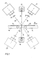
- the apparatus shown in the drawing for detecting cracks in a semiconductor wafer 11, in particular a silicon wafer, has a transport device 12, by which the semiconductor wafer in the transport direction 13 is movable.
- the transport device comprises two conveyor belts 14, which are spaced apart leaving a gap 15 in the transport direction.
- the gap is sized so that it can be straddled by the semiconductor wafer as shown in FIGS. 1 and 2.
- a first luminaire 16 is provided, which emits light in the infrared range and illuminates the semiconductor wafer 11 in the region of the gap 15 over its entire width in the direction perpendicular to the drawing plane.
- the semiconductor wafer is transparent to infrared light so that at least a portion of the incident light passes through the wafer.
- an infrared sensitive electronic camera 17 is provided which receives the passing light.
- the camera can be provided with a corresponding optical filter 21.
- the lamp 16 may be formed as a broadband lamp with a wide wavelength spectrum and be provided for example with a corresponding filter for generating infrared light.
- the arrangement is such that the camera is a line scan camera and has an optical axis 18 that is at an angle to the plane 19 containing the line light.
- the passing light does not hit directly into the lens of the camera, but the camera takes in the so-called dark field without direct incidence of light on the surface facing away from the lamp 16 20 of the wafer resulting light strip on. Unwanted or critical exposure situations in the edge region of the wafer can thus be avoided.
- a second luminaire 22 which illuminates the surface 20 of the wafer with visible light.
- this lamp is arranged on the side of the wafer 11 opposite the infrared lamp 16.
- the luminaire also produces a line light that preferably illuminates the same portion of the wafer in the region of the gap 15 as the line light of the infrared illuminator 16.
- the optical axis 25 of the camera extends at an angle to the plane 26 containing the line light of the luminaire 22.
- the sensitivity of the camera can be adjusted by means of a corresponding filter 24.
- the lamp 22 may be formed as a broadband lamp with a wide wavelength spectrum and be provided for example with a corresponding filter for generating visible light.
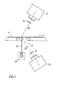
- a lamp 27 is provided, which is designed as a broadband light with a wide wavelength spectrum and emits both infrared light and light in the visible range.
- the luminaire generates a line light which illuminates the wafer in the region of the gap 15 over its entire width illuminated linearly in the direction perpendicular to the drawing plane.
- an infrared sensitive camera 17 is arranged, which receives the light passing through the wafer. Again, the optical axis 18 of the camera is at an angle to the plane 30 of the line light.
- a visible-light camera 23 which receives the light scattered and / or diffracted at the wafer. In this arrangement of FIG. 2, only one light is required. However, the camera 23 can also be sensitive to infrared light and record, for example, the non-transmitted portion of the infrared light. Then an infrared light can be enough.
- both surfaces of the wafer are optically scanned with visible light.
- this possibility is shown with a further sensitive to visible light camera 23 'by dashed lines.
- the light 16 is designed as a broadband light.
- the cameras 17, 17 ', 23, 23' are designed as line scan cameras and the line-shaped sensor runs parallel to the width of the wafer perpendicular to the plane of the drawing.
- the movement of the wafer perpendicular to the line direction of the cameras produces line-shaped images of the wafer once under infrared illumination and once under illumination with visible light. This allows areas with possible cracks to be selected. The cracks can then be recognized in the course of further image processing.
- the light plane 19, 26, 30 runs perpendicular to the surface of the wafer for generating the line light.
- the optical axes 18, 25 of the cameras 17, 23, 17 ', 23' extend at an angle deviating from 90 ° to the wafer.
- other angular arrangements may be provided.
- the optical axes may be at a right angle to the wafer while the light planes extend at an oblique angle to the wafer.
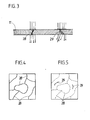
- the wafers are usually thin plates that consist of a variety of crystals. Individual crystals are separated by grain boundaries 28. Furthermore, cracks 29 can occur, which can often cause rapid breakage of the inherently brittle wafer. Semiconductor wafers, and especially silicon wafers, are transparent to infrared light. In FIG. 3, the beam path of the infrared light through a wafer in the region of a crack 29 and a grain boundary 28 is shown schematically. Both the crack 29 and the grain boundary 28 will cause a deflection of the passing light, so that these areas in the generated image as a contrast and usually appear dark.
- FIG. 4 schematically shows the image of a portion of a wafer surface having grain boundaries 28 as formed upon exposure of a visible light camera.
- Fig. 5 shows the image of the same section as formed during the exposure of a camera with infrared light. The grain boundaries 28 will still be visible, but additionally the cracks 29 will be imaged.
- the areas with possible cracks can be detected.
- the grain boundaries can be eliminated by the generation of a difference image, provided that the grain boundaries are imaged identically both under infrared light and under visible light. This is not always the case, so that grain boundaries also appear as line-shaped phenomena as possible cracks. However, these can be distinguished from the actual cracks by known image processing steps, such as edge and line recognition methods. With this structure, semiconductor wafers can be inspected for cracks quickly and reliably.
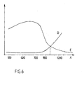
- the wavelength range of the infrared light with respect to the sensitivity of the sensor and the permeability of the wafer must be optimized.
- FIG. 1 the sensitivity E of a sensor and the transmittance D of the wafer are plotted against the wavelength ⁇ . In the range between 900 nm and 1200 nm, the sensitivity decreases sharply while the transmittance increases.
- An intersection point can be determined which marks a favorable wavelength range. In the example shown in Fig. 6, the point of intersection is at a wavelength of about 1000 nm, at which the photosensitive receiver is still sensitive and the wafer is already well permeable. It can then be generated high-contrast images with sufficient light intensity.
Applications Claiming Priority (1)
| Application Number | Priority Date | Filing Date | Title |
|---|---|---|---|
| DE200510061785 DE102005061785B4 (de) | 2005-12-23 | 2005-12-23 | Verfahren und Vorrichtung zum Erkennen von Rissen in Silizium-Wafern |
Publications (2)
| Publication Number | Publication Date |
|---|---|
| EP1801569A2 true EP1801569A2 (fr) | 2007-06-27 |
| EP1801569A3 EP1801569A3 (fr) | 2008-07-23 |
Family
ID=37801467
Family Applications (1)
| Application Number | Title | Priority Date | Filing Date |
|---|---|---|---|
| EP06023194A Withdrawn EP1801569A3 (fr) | 2005-12-23 | 2006-11-08 | Procédé et dispositif destinés à la reconnaissance de fissures dans des tranches de silicium |
Country Status (2)
| Country | Link |
|---|---|
| EP (1) | EP1801569A3 (fr) |
| DE (1) | DE102005061785B4 (fr) |
Cited By (18)
| Publication number | Priority date | Publication date | Assignee | Title |
|---|---|---|---|---|
| EP1956366A1 (fr) * | 2007-02-06 | 2008-08-13 | Basler AG | Procédé et dispositif destinés à la détection de défauts |
| WO2008110159A2 (fr) * | 2007-03-15 | 2008-09-18 | Gp Solar Gmbh | Procédé et dispositif permettant de déterminer une rupture dans une matière cristalline |
| WO2009027517A1 (fr) * | 2007-08-31 | 2009-03-05 | Icos Vision Systems Nv | Appareil et procédé de détection d'anomalies d'un substrat semi-conducteur |
| WO2010007617A2 (fr) * | 2008-07-14 | 2010-01-21 | Brightview Systems Ltd. | Procédé et appareil de contrôle de la qualité de films minces |
| ITUD20090119A1 (it) * | 2009-06-22 | 2010-12-23 | Applied Materials Inc | Sistema di visione migliorato per l'allineamento di uno schema di stampa serigrafica |
| DE102009039685A1 (de) * | 2009-09-02 | 2011-03-03 | Gp Inspect Gmbh | Verfahren und Vorrichtung zur Detektion von Defekten in einem Objekt |
| EP2316127A1 (fr) * | 2008-07-28 | 2011-05-04 | Bluplanet Pte Ltd | Procede et systeme pour detecter des micro-fissures dans des plaquettes |
| WO2011079354A1 (fr) * | 2010-01-04 | 2011-07-07 | Bt Imaging Pty Ltd | Imagerie par photoluminescence en cours de production de dispositifs semi-conducteurs |
| EP2351073A1 (fr) * | 2008-11-25 | 2011-08-03 | Bluplanet Pte Ltd | Appareil de détection de microfissures dans des tranches et procédé associé |
| EP2359410A1 (fr) * | 2008-12-10 | 2011-08-24 | Applied Materials, Inc. | Système de visualisation amélioré pour calage de motif de sérigraphie |
| WO2014095615A1 (fr) * | 2012-12-17 | 2014-06-26 | Bundesdruckerei Gmbh | Procédé et dispositif pour fabriquer un document de valeur et/ou de sécurité comprenant une structure d'antenne |
| JP5559163B2 (ja) * | 2009-05-29 | 2014-07-23 | 株式会社ロゼフテクノロジー | 多結晶ウエハの検査方法 |
| JP2014190797A (ja) * | 2013-03-27 | 2014-10-06 | Tokushima Densei Kk | シリコンウェハの欠陥検査装置 |
| CN104916561A (zh) * | 2014-03-12 | 2015-09-16 | 晶元光电股份有限公司 | 管芯检测方法 |
| US9255893B2 (en) | 2011-04-18 | 2016-02-09 | Kla-Tencor Corporation | Apparatus for illuminating substrates in order to image micro cracks, pinholes and inclusions in monocrystalline and polycrystalline substrates and method therefore |
| EP3081901A1 (fr) * | 2015-04-17 | 2016-10-19 | Hennecke Systems GmbH | Procédé et dispositif d'inspection permettant d'inspecter un motif de surface |
| DE102016223306A1 (de) * | 2016-11-24 | 2018-05-24 | Bayerische Motoren Werke Aktiengesellschaft | Vorrichtung und Verfahren zur Detektion von Defekten eines Prüfobjekts |
| US10724965B2 (en) | 2018-02-09 | 2020-07-28 | Massachusetts Institute Of Technology | Systems and methods for crack detection |
Families Citing this family (1)
| Publication number | Priority date | Publication date | Assignee | Title |
|---|---|---|---|---|
| DE102016224767B4 (de) * | 2016-12-13 | 2019-08-08 | Bayerische Motoren Werke Aktiengesellschaft | Vorrichtung und Verfahren zur Detektion von Defekten eines Prüfobjekts |
Citations (5)
| Publication number | Priority date | Publication date | Assignee | Title |
|---|---|---|---|---|
| JPH08220008A (ja) * | 1995-02-15 | 1996-08-30 | Mitsubishi Electric Corp | 赤外検査装置 |
| JPH1090192A (ja) * | 1996-08-29 | 1998-04-10 | Kla Instr Corp | 試料からの多重チャネル応答を用いた試料の光学的検査 |
| EP1001460A1 (fr) * | 1998-10-15 | 2000-05-17 | Wacker Siltronic Gesellschaft für Halbleitermaterialien Aktiengesellschaft | Procédé et appareil pour détecter, surveiller et caractériser des défauts de bordure sur les plaquettes semiconductrices |
| WO2005100961A2 (fr) * | 2004-04-19 | 2005-10-27 | Phoseon Technology, Inc. | Structures semi-conductrices d'imagerie utilisant un eclairage a semi-conducteurs |
| US20050264797A1 (en) * | 2004-05-26 | 2005-12-01 | Hiroyuki Nakano | Method and apparatus for detecting defects |
Family Cites Families (2)
| Publication number | Priority date | Publication date | Assignee | Title |
|---|---|---|---|---|
| DE19733431A1 (de) * | 1997-03-13 | 1998-09-17 | Tema Teubner & Mandewirth Gmbh | Anordnung von Fehlerüberwachung |
| DE10122313A1 (de) * | 2001-05-08 | 2002-11-21 | Wolfgang P Weinhold | Verfahren und Vorrichtung zur berührungsfreien Untersuchung eines Gegenstandes, insbesondere hinsichtlich dessen Oberflächengestalt |
-
2005
- 2005-12-23 DE DE200510061785 patent/DE102005061785B4/de not_active Expired - Fee Related
-
2006
- 2006-11-08 EP EP06023194A patent/EP1801569A3/fr not_active Withdrawn
Patent Citations (5)
| Publication number | Priority date | Publication date | Assignee | Title |
|---|---|---|---|---|
| JPH08220008A (ja) * | 1995-02-15 | 1996-08-30 | Mitsubishi Electric Corp | 赤外検査装置 |
| JPH1090192A (ja) * | 1996-08-29 | 1998-04-10 | Kla Instr Corp | 試料からの多重チャネル応答を用いた試料の光学的検査 |
| EP1001460A1 (fr) * | 1998-10-15 | 2000-05-17 | Wacker Siltronic Gesellschaft für Halbleitermaterialien Aktiengesellschaft | Procédé et appareil pour détecter, surveiller et caractériser des défauts de bordure sur les plaquettes semiconductrices |
| WO2005100961A2 (fr) * | 2004-04-19 | 2005-10-27 | Phoseon Technology, Inc. | Structures semi-conductrices d'imagerie utilisant un eclairage a semi-conducteurs |
| US20050264797A1 (en) * | 2004-05-26 | 2005-12-01 | Hiroyuki Nakano | Method and apparatus for detecting defects |
Non-Patent Citations (1)
| Title |
|---|
| HODOR J R ET AL: "Optical sensor designs for the detection of cracks in optical materials" PROCEEDINGS OF THE SPIE, SPIE, BELLINGHAM, VA, Bd. 1168, 1. Januar 1989 (1989-01-01), Seiten 138-146, XP009100242 ISSN: 0277-786X * |
Cited By (35)
| Publication number | Priority date | Publication date | Assignee | Title |
|---|---|---|---|---|
| EP1956366A1 (fr) * | 2007-02-06 | 2008-08-13 | Basler AG | Procédé et dispositif destinés à la détection de défauts |
| WO2008110159A2 (fr) * | 2007-03-15 | 2008-09-18 | Gp Solar Gmbh | Procédé et dispositif permettant de déterminer une rupture dans une matière cristalline |
| WO2008110159A3 (fr) * | 2007-03-15 | 2008-11-20 | Gp Solar Gmbh | Procédé et dispositif permettant de déterminer une rupture dans une matière cristalline |
| WO2009027517A1 (fr) * | 2007-08-31 | 2009-03-05 | Icos Vision Systems Nv | Appareil et procédé de détection d'anomalies d'un substrat semi-conducteur |
| US8379964B2 (en) | 2007-08-31 | 2013-02-19 | Kla-Tencor Corporation | Detecting semiconductor substrate anomalies |
| CN101796398B (zh) * | 2007-08-31 | 2013-06-19 | Icos视觉系统股份有限公司 | 用于检测半导体异常的装置和方法 |
| WO2010007617A2 (fr) * | 2008-07-14 | 2010-01-21 | Brightview Systems Ltd. | Procédé et appareil de contrôle de la qualité de films minces |
| WO2010007617A3 (fr) * | 2008-07-14 | 2010-03-18 | Brightview Systems Ltd. | Procédé et appareil de contrôle de la qualité de films minces |
| EP2316127A4 (fr) * | 2008-07-28 | 2013-12-04 | Bluplanet Pte Ltd | Procede et systeme pour detecter des micro-fissures dans des plaquettes |
| EP2316127A1 (fr) * | 2008-07-28 | 2011-05-04 | Bluplanet Pte Ltd | Procede et systeme pour detecter des micro-fissures dans des plaquettes |
| EP2351073A1 (fr) * | 2008-11-25 | 2011-08-03 | Bluplanet Pte Ltd | Appareil de détection de microfissures dans des tranches et procédé associé |
| EP2351073A4 (fr) * | 2008-11-25 | 2014-01-22 | Bluplanet Pte Ltd | Appareil de détection de microfissures dans des tranches et procédé associé |
| EP2359410A1 (fr) * | 2008-12-10 | 2011-08-24 | Applied Materials, Inc. | Système de visualisation amélioré pour calage de motif de sérigraphie |
| EP2359410A4 (fr) * | 2008-12-10 | 2014-09-24 | Applied Materials Inc | Système de visualisation amélioré pour calage de motif de sérigraphie |
| JP5559163B2 (ja) * | 2009-05-29 | 2014-07-23 | 株式会社ロゼフテクノロジー | 多結晶ウエハの検査方法 |
| ITUD20090119A1 (it) * | 2009-06-22 | 2010-12-23 | Applied Materials Inc | Sistema di visione migliorato per l'allineamento di uno schema di stampa serigrafica |
| US8400630B2 (en) | 2009-09-02 | 2013-03-19 | Gp Inspect Gmbh | Method and device for the detection of defects in an object |
| CN102004107B (zh) * | 2009-09-02 | 2015-06-24 | Gp检验有限公司 | 用于探测对象中的缺陷的方法和装置 |
| DE102009039685B4 (de) * | 2009-09-02 | 2015-07-16 | Gp Inspect Gmbh | Verfahren und Vorrichtung zur Detektion von Defekten in einem Objekt |
| DE102009039685A8 (de) * | 2009-09-02 | 2011-06-01 | Gp Inspect Gmbh | Verfahren und Vorrichtung zur Detektion von Defekten in einem Objekt |
| DE102009039685A1 (de) * | 2009-09-02 | 2011-03-03 | Gp Inspect Gmbh | Verfahren und Vorrichtung zur Detektion von Defekten in einem Objekt |
| CN102004107A (zh) * | 2009-09-02 | 2011-04-06 | Gp检验有限公司 | 用于探测对象中的缺陷的方法和装置 |
| WO2011079354A1 (fr) * | 2010-01-04 | 2011-07-07 | Bt Imaging Pty Ltd | Imagerie par photoluminescence en cours de production de dispositifs semi-conducteurs |
| CN102812349B (zh) * | 2010-01-04 | 2016-03-09 | Bt成像股份有限公司 | 半导体设备的在线光致发光成像 |
| US9035267B2 (en) | 2010-01-04 | 2015-05-19 | Bt Imaging Pty Ltd | In-line photoluminescence imaging of semiconductor devices |
| CN102812349A (zh) * | 2010-01-04 | 2012-12-05 | Bt成像股份有限公司 | 半导体设备的在线光致发光成像 |
| US9255893B2 (en) | 2011-04-18 | 2016-02-09 | Kla-Tencor Corporation | Apparatus for illuminating substrates in order to image micro cracks, pinholes and inclusions in monocrystalline and polycrystalline substrates and method therefore |
| WO2014095615A1 (fr) * | 2012-12-17 | 2014-06-26 | Bundesdruckerei Gmbh | Procédé et dispositif pour fabriquer un document de valeur et/ou de sécurité comprenant une structure d'antenne |
| JP2014190797A (ja) * | 2013-03-27 | 2014-10-06 | Tokushima Densei Kk | シリコンウェハの欠陥検査装置 |
| CN104916561A (zh) * | 2014-03-12 | 2015-09-16 | 晶元光电股份有限公司 | 管芯检测方法 |
| CN104916561B (zh) * | 2014-03-12 | 2019-06-18 | 晶元光电股份有限公司 | 管芯检测方法 |
| EP3081901A1 (fr) * | 2015-04-17 | 2016-10-19 | Hennecke Systems GmbH | Procédé et dispositif d'inspection permettant d'inspecter un motif de surface |
| WO2016166593A1 (fr) * | 2015-04-17 | 2016-10-20 | Hennecke Systems Gmbh | Procédé t dispositif d'inspection pour inspecter un motif de surface |
| DE102016223306A1 (de) * | 2016-11-24 | 2018-05-24 | Bayerische Motoren Werke Aktiengesellschaft | Vorrichtung und Verfahren zur Detektion von Defekten eines Prüfobjekts |
| US10724965B2 (en) | 2018-02-09 | 2020-07-28 | Massachusetts Institute Of Technology | Systems and methods for crack detection |
Also Published As
| Publication number | Publication date |
|---|---|
| EP1801569A3 (fr) | 2008-07-23 |
| DE102005061785A1 (de) | 2007-07-05 |
| DE102005061785B4 (de) | 2008-04-03 |
Similar Documents
| Publication | Publication Date | Title |
|---|---|---|
| DE102005061785B4 (de) | Verfahren und Vorrichtung zum Erkennen von Rissen in Silizium-Wafern | |
| DE102007006525B4 (de) | Verfahren und Vorrichtung zur Detektierung von Defekten | |
| DE102009039685B4 (de) | Verfahren und Vorrichtung zur Detektion von Defekten in einem Objekt | |
| EP1769689B1 (fr) | Dispositif et procédé pour déterminer les caractéristiques de filtres composés ou d'assemblages d'éléments à filtre | |
| EP2494339B1 (fr) | Procédé et dispositif de détection de fissures dans des substrats semi-conducteurs | |
| DE1448409A1 (de) | Geraet zum automatischen Pruefen eines Gegenstandes | |
| DE2436110C3 (de) | Vorrichtung zur Feststellung von Herstellungsfehlern in einer bewegten Materialbahn | |
| DE3926349C2 (fr) | ||
| EP1198704B1 (fr) | Procede et dispositif d'inspection de receptacles transparents | |
| WO2010121753A1 (fr) | Procédé de détection des défauts d'une mince tranche pour un élément solaire ainsi que dispositif de mise en oeuvre du procédé | |
| EP3134726B1 (fr) | Procédé et dispositif permettant de détecter des inclusions de sulfure de nickel dans une plaque de verre | |
| DE10324474A1 (de) | Vorrichtung zur Wafer-Inspektion | |
| EP2144052A1 (fr) | Procédé et dispositif de détection et de classification de défauts | |
| WO2018024550A1 (fr) | Dispositif et procédé pour déterminer un angle d'image double et/ou un angle de visée | |
| DE2001990A1 (de) | Verfahren und elektrooptisches System zur Untersuchung von Koerpern,wie z.B. Fliesen | |
| DE3022750A1 (de) | Abtastvorrichtung fuer einen beweglichen gegenstand | |
| WO1996038370A1 (fr) | Procede de surveillance en direct de bordures de bandes au moyen de cameras de ligne | |
| EP2831570B1 (fr) | Procédé pour la détection de couches enterrées | |
| DE19732831C2 (de) | Verfahren und Vorrichtung zum Abtasten einer vorzugsweise textilen Warenbahn | |
| DE1919879A1 (de) | Vorrichtung zum Nachweisen von Oberflaechenfehlern | |
| EP0052812A2 (fr) | Procédé pour la détection des déviations d'un signal, utilisant un amplificateur différentiel intégrateur | |
| DE4200801A1 (de) | Vorrichtung zur durchfuehrung einer qualitaetskontrolle | |
| DE102015114575B4 (de) | Vorrichtung zur Druckbildkontrolle | |
| DE112016006757T5 (de) | Verfahren und System zur Überwachung eines Laserstrukturierungsvorgangs zur Bildung von Isolationsgräben in einem Solarmodul | |
| WO2018007215A1 (fr) | Dispositif et procédé d'inspection d'objets à verre de protection |
Legal Events
| Date | Code | Title | Description |
|---|---|---|---|
| PUAI | Public reference made under article 153(3) epc to a published international application that has entered the european phase |
Free format text: ORIGINAL CODE: 0009012 |
|
| AK | Designated contracting states |
Kind code of ref document: A2 Designated state(s): AT BE BG CH CY CZ DE DK EE ES FI FR GB GR HU IE IS IT LI LT LU LV MC NL PL PT RO SE SI SK TR |
|
| AX | Request for extension of the european patent |
Extension state: AL BA HR MK YU |
|
| PUAL | Search report despatched |
Free format text: ORIGINAL CODE: 0009013 |
|
| AK | Designated contracting states |
Kind code of ref document: A3 Designated state(s): AT BE BG CH CY CZ DE DK EE ES FI FR GB GR HU IE IS IT LI LT LU LV MC NL PL PT RO SE SI SK TR |
|
| AX | Request for extension of the european patent |
Extension state: AL BA HR MK RS |
|
| 17P | Request for examination filed |
Effective date: 20090115 |
|
| AKX | Designation fees paid |
Designated state(s): AT BE BG CH CY CZ DE DK EE ES FI FR GB GR HU IE IS IT LI LT LU LV MC NL PL PT RO SE SI SK TR |
|
| 17Q | First examination report despatched |
Effective date: 20090406 |
|
| STAA | Information on the status of an ep patent application or granted ep patent |
Free format text: STATUS: THE APPLICATION IS DEEMED TO BE WITHDRAWN |
|
| 18D | Application deemed to be withdrawn |
Effective date: 20091217 |