EP1793497A1 - Device and method for reading a capacitive sensor, in particular of a micro-electromechanical type - Google Patents
Device and method for reading a capacitive sensor, in particular of a micro-electromechanical type Download PDFInfo
- Publication number
- EP1793497A1 EP1793497A1 EP05425863A EP05425863A EP1793497A1 EP 1793497 A1 EP1793497 A1 EP 1793497A1 EP 05425863 A EP05425863 A EP 05425863A EP 05425863 A EP05425863 A EP 05425863A EP 1793497 A1 EP1793497 A1 EP 1793497A1
- Authority
- EP
- European Patent Office
- Prior art keywords
- read
- electrical
- terminal
- signal
- capacitive sensor
- Prior art date
- Legal status (The legal status is an assumption and is not a legal conclusion. Google has not performed a legal analysis and makes no representation as to the accuracy of the status listed.)
- Granted
Links
Images


Classifications
-
- G—PHYSICS
- G01—MEASURING; TESTING
- G01P—MEASURING LINEAR OR ANGULAR SPEED, ACCELERATION, DECELERATION, OR SHOCK; INDICATING PRESENCE, ABSENCE, OR DIRECTION, OF MOVEMENT
- G01P15/00—Measuring acceleration; Measuring deceleration; Measuring shock, i.e. sudden change of acceleration
- G01P15/02—Measuring acceleration; Measuring deceleration; Measuring shock, i.e. sudden change of acceleration by making use of inertia forces using solid seismic masses
- G01P15/08—Measuring acceleration; Measuring deceleration; Measuring shock, i.e. sudden change of acceleration by making use of inertia forces using solid seismic masses with conversion into electric or magnetic values
- G01P15/125—Measuring acceleration; Measuring deceleration; Measuring shock, i.e. sudden change of acceleration by making use of inertia forces using solid seismic masses with conversion into electric or magnetic values by capacitive pick-up
Definitions
- the present invention relates to a device and to a method for reading a capacitive sensor, in particular of a micro-electromechanical type.
- capacitive inertial micro-electromechanical-system (MEMS) sensors of a differential type are increasingly frequently used in a wide range of portable electronic devices, such as cellphones, palm-top computers, digital camcorders and cameras, and the like, which are supplied autonomously by batteries.
- MEMS micro-electromechanical-system
- CDS correlated-double-sampling
- Figures 1-3 show the different steps for reading a capacitive inertial sensor 1 of a differential MEMS type, using the CDS technique.
- the inertial sensor 1 is represented by means of an equivalent electrical diagram and comprises a first sense capacitor 2a and a second sense capacitor 2b having a first common terminal, which forms a driving terminal 1c of the inertial sensor 1.
- Second terminals of the first sense capacitor 2a and of the second sense capacitor 2b form a first sense terminal 1a and, respectively, a second sense terminal 1b of the inertial sensor 1.
- the two capacitors 2a, 2b have differentially variable capacitances, i.e., they have the same capacitance at rest C S , when the inertial sensor 1 is not subjected to the quantity to be sensed, and show capacitance variations of equal amplitude and opposite sign when the inertial sensor 1 senses a quantity along a pre-set axis.
- a read circuit 3 is associated to the inertial sensor 1 and comprises a signal source 4, a charge-voltage converter 5, and a cancelling stage 7.
- the signal source 4 is connected to the driving terminal 1c of the inertial sensor 1 and supplies a step read voltage V RD .
- the charge-voltage converter 5 includes a fully differential switched-capacitor charge amplifier 10, having a first integration capacitor 11a connected between a first input and a first output and a second integration capacitor 11b connected between a second input and a second output. Furthermore, the first input and the second input of the charge amplifier 10 are connected to the first sense terminal 1a and to the second sense terminal 1b of the inertial sensor 1, respectively.
- the cancelling stage 7 comprises a first hold capacitor 12a and a second hold capacitor 12b, respectively connected in series to the first output and to the second output of the charge amplifier 10. Furthermore, terminals of the first hold capacitor 12a and of the second hold capacitor 12b form a first output 3a and, respectively, a second output 3b of the read circuit 3.
- the signal source 4 sends the driving terminal 1c of the inertial sensor 1 to a ground value.
- the first input and the second input of the charge amplifier 10 are instead brought to a reference line 15, which supplies a constant reference voltage V REF , whereas the first output and the second output are short-circuited.
- first reset switches 16a, 1b connected between the reference line 15 and a respective input of the charge amplifier 10, and a second reset switch 16c, arranged between the outputs of the charge amplifier 10 itself, go into a closed condition.
- a second step, or offset-cancelling step the first reset switches 16a, 16b and the second reset switch 16c are opened condition, while the driving terminal 1c of the inertial sensor 1 is still kept at the ground voltage. Furthermore, a first cancelling switch 18a, connected between the reference line 15 and the first output 3a, and a second cancelling switch 18b, connected between the reference line 15 and the second output 3b, are closed. In this way, any possible disturbance, such as 1/f noise, and a possible offset introduced by the charge amplifier 10 cause a cancelling voltage V C between the outputs by the charge amplifier 10 itself.
- the cancelling voltage V C is in practice stored in the first hold capacitor 12a and in the second hold capacitor 12b.
- a third step or sensing step is executed, in which the first reset switches 16a, 16b, the second reset switch 16c, and the cancelling switches 18a, 18b are opened, and the signal source (illustrated with a solid line) supplies the step read voltage V RD to the driving terminal 1c of the inertial sensor 1.
- the signal source illustrated with a solid line
- a first sense charge Q A and, respectively, a second sense charge Q B correlated to the capacitive unbalancing of the inertial sensor 1 are supplied to the inputs of the charge amplifier 10 and converted into a rough output voltage V OR , which includes the contributions of noise and of offset due to the charge amplifier 10.
- the cancelling stage 7 subtracts the cancelling voltage V C , stored by the first hold capacitor 12a and the second hold capacitor 12b.
- the read circuit 3 supplies a corrected output voltage V OC , which substantially is not affected by the contribution of the low-frequency noise and of the offsets introduced by the electronics.
- the CDS technique does not, however, enable suppression of the low-frequency disturbance generated upstream of the charge amplifier 10.
- Said disturbance can have different origins, but, basically, takes the form of a differential disturbance current I D supplied in parallel to the currents due to the injection of charge (Q A , Q B ) performed by the inertial sensor 1 (the disturbance is represented schematically by a current generator 20 in Figure 4).
- an important source of disturbance is represented by the first reset switches, which, even when opened, have dispersion currents (of an intensity of up to a few nanoamps).
- the aim of the present invention is to provide a device and a method for reading a capacitive sensor, which will enable the drawbacks described above to be overcome.
- a device and a method for reading a capacitive sensor are provided, as defined in Claims 1 and 18, respectively.
- Illustrated in Figure 5 and designated by the reference number 100 is an apparatus for detecting accelerations, comprising an inertial sensor 101 of a differential capacitive MEMS type, and a read device 103, associated to the inertial sensor 101.
- an inertial sensor 101 of a differential capacitive MEMS type comprising an inertial sensor 101 of a differential capacitive MEMS type, and a read device 103, associated to the inertial sensor 101.
- the example that will be described hereinafter must not, however, be considered limiting in so far as the invention can be used for reading capacitive sensors of any type.
- the inertial sensor 101 in itself known, comprises a movable body (not illustrated), which is movable with respect to a fixed body (which is not illustrated either) and is capacitively coupled thereto so as to form in practice a first sense capacitor 102a, and a second sense capacitor 102b (see for this item Figure 7).
- the capacitance of the first sense capacitor 102a and second sense capacitor 102b depend on the relative position of the movable body with respect to the fixed body and vary in a differential way.
- the first sense capacitor 102a and the second sense capacitor 102b have the same rest capacitance C S when the inertial sensor 1 is not subjected to the quantity to be sensed, and show capacitance variations ⁇ C S of equal amplitude and opposite sign when the inertial sensor 1 senses an acceleration along a predetermined axis.
- disturbance caused by the inertial sensor 101 is represented schematically by a current generator 150, which injects a disturbance current I D into the input of the read device 103.
- the read device 103 is of the discrete-time type and comprises a signal source 104, a modulator stage 105, a sense circuit 107, a demodulator stage 110, and a lowpass filter 112. Furthermore, a phase-generator stage 113 generates a plurality of timing signals S 1 -S 6 , necessary for co-ordinating operation of the different components of the read device 103.
- the phase-generator stage 113 comprises an oscillator 113a and a plurality of timing modules C1-C6, controlled by the oscillator 113a, each of which generates a respective timing signal S 1 -S 6 .
- the signal source 104 supplies a step read voltage V RD , preferably of an amplitude equal to the maximum dynamics available, which, in the embodiment described, is equal to the supply voltage V DD (for example, 3 V).
- the modulator stage 105 is arranged between the signal source 104 and the inertial sensor 101 and modulates the read voltage V RD , multiplying it at each read cycle alternately by +1 and -1 (for example, the reading frequency is comprised between 10 and 100 kHz).
- a square-wave modulated read voltage V RDM is present on the output of the modulator stage 105 and is supplied to the inertial sensor 101. Reading of the inertial sensor 101 is performed on each edge, both the leading edge and the trailing edge, of the modulated read voltage V RDM .
- the sense circuit 107 comprises a charge-voltage converter 108 and a cancelling stage 109.
- the charge-voltage converter 108 of the switched-capacitor type, is set downstream of the inertial sensor 101.
- the charge-voltage converter 108 receives a first sense charge Q A and a second sense charge Q B , which are supplied by the inertial sensor 101 in response to the modulated read voltage V RDM and are correlated to the differential variations of capacitance ⁇ C S of the first sense capacitor 102a and of the second sense capacitor 102b.
- the cancelling stage 109 is connected in series to outputs of the charge-voltage converter 108 and is used for cancelling the offset and the low-frequency noise introduced by the charge-voltage converter 108 itself.
- a modulated output voltage V OM is present between the outputs of the cancelling stage 109.
- the demodulator 110 is cascaded to the cancelling stage 109, for receiving the modulated output voltage V OM , which is again multiplied alternately by +1 and -1 at each read cycle and converted into a demodulated output voltage V OD .
- the lowpass filter 112 receives the demodulated output voltage V OD , eliminates the high-frequency components, and supplies a corrected output voltage V OC .
- the read device 103 enables suppression also of the disturbance due to the inertial sensor 101, in addition to the low-voltage noise and to the offset introduced by the charge-voltage converter 108.
- the modulation in fact, enables separation of the harmonic content of the read voltage V RD and of the variations of capacitance ⁇ C S from that of the disturbance caused by the inertial sensor 101.
- the modulation translates at high frequency the spectrum of the variations of capacitance ⁇ C S that are linked to the quantities detected by the inertial sensor 101 (i.e., the useful signal, Figures 6a and 6b), whereas the disturbance components, which intervene downstream of the charge-voltage converter 108, remain in base band (Figure 6c, modulated output voltage V OM ).
- the demodulation in practice reverses the content, and hence the useful component, which contains the information on the variations of capacitance ⁇ C S of the inertial sensor 1, is brought back into the base band, whereas the disturbance component is translated at high frequency (Figure 6d, demodulated output voltage V OD ).
- the disturbance can then readily be eliminated by the lowpass filter 112, provided that the reading frequency is sufficiently high (Figure 6e, corrected output voltage V OC ; the harmonic components linked to the disturbance that are suppressed and the transfer function of the lowpass filter 112 are respectively represented by a dashed line and dashed and dotted line).
- FIG. 7 shows a more detailed circuit implementation of the acceleration-detection apparatus 100.
- the inertial sensor 101 is represented schematically by the first sense capacitor 102a and the second sense capacitor 102b, which have a common terminal forming the driving input 101c and respective second terminals forming a first sense terminal 101a and a second sense terminal 101b.
- the signal source 104 and the modulator stage 105 are formed by a single circuit, hereinafter referred to as modulated source 106, comprising a ground line 115, set at a ground voltage V GND (0 V), a supply line 116, supplying a supply voltage V DD , and a first read switch 118a and a second read switch 118b, respectively controlled by a first timing signal S 1 and a second timing signal S 2 (the first timing signal S 1 and the second timing signal S 2 are generated by a first timer module C1 and by a second timer module C2, respectively).
- modulated source 106 comprising a ground line 115, set at a ground voltage V GND (0 V), a supply line 116, supplying a supply voltage V DD , and a first read switch 118a and a second read switch 118b, respectively controlled by a first timing signal S 1 and a second timing signal S 2 (the first timing signal S 1 and the second timing signal S 2 are generated by a first timer module C1
- first read switch 118a and the second read switch 118b have a terminal in common connected to the driving terminal 101c of the inertial sensor 101; moreover, the first read switch 118a is connected to the ground line 115, whereas the second read switch 118b is connected to the supply line 116.
- the charge-voltage converter 108 comprises a fully differential switched-capacitor charge amplifier 120, having a first integration capacitor 121a connected between a first input and a first (non-inverting) output and a second integration capacitor 121b connected between a second input and a second (inverting) output.
- the first input and the second input of the charge amplifier 120 are connected to the first sense terminal 101a and, respectively, to the second sense terminal 101b of the inertial sensor 101.
- the first input and the second input of the charge amplifier 120 can be selectively connected to a reference line 123, supplying a constant reference voltage V REF by a first reset switch 125a and, respectively, a second reset switch 125b.
- a third reset switch is connected between the outputs of the charge amplifier 120. All the reset switches 125a, 125b, 125c are controlled by one and the same third timing signal S 3 , generated by a third timer module C3 of the phase-generator stage 113.
- the cancelling stage 109 comprises a first hold capacitor 122a and a second hold capacitor 122b, respectively connected in series to the first output and to the second output of the charge amplifier 109.
- the demodulator stage 110 has a first input 110a and a second input 110b and a first output 110c and a second output 110d.
- a first direct-connection switch 127a and a second direct-connection switch 127b are connected between the first input 110a and the first output 110c and between the second input 110b and the second output 110d, respectively, and are controlled by a same fourth timing signal S 4 generated by a fourth timer module C4.
- a first crossed-connection switch 127c and a second crossed-connection switch 127d are connected between the first input 110a and the second output 110d and between the second input 110b and the first output 110c, respectively, and are controlled by a same fifth timing signal S 5 generated by a fifth timer module C5.
- the direct-connection switches 127a, 127b and the crossed-connection switches 127c, 127d are controlled so that the connection between the inputs 110a, 110b and the outputs 110c, 110d of the demodulator stage 110 is reversed in consecutive read cycles.
- the first input 110a is connected to the first output 110c and the second input 110b is connected to the second output 110d
- the sign of the demodulated output voltage V OD is once equal (multiplication by +1) and once opposite (multiplication by -1) to the sign of the modulated output voltage V OM .
- the first output 110c and the second output 110d of the demodulator stage 110 are moreover selectively connectable to the reference line 123 by a first cancelling switch 128a and, respectively, a second cancelling switch 128b, which are controlled by a same sixth timing signal S 6 , generated by a sixth timer module C6 of the phase-generator stage 113.
- the lowpass filter 112 is of a discrete-time analog type and is substantially configured so as to calculate the arithmetic mean of pairs (or in any case an even number) of successive samples of the demodulated output voltage V OD .
- the corrected output voltage V OC is hence proportional to said arithmetic mean.
- Figure 8a-8g represent time plots corresponding to the modulated read voltage V RDM ( Figure 8a) and to the timing signals S 1 -S 6 ( Figures 8b-8g) during two consecutive read cycles RD K , RID K+1 .
- Figure 8h illustrates the theoretical evolution of the read voltage V RD , which is not visible in the read device 103 illustrated in Figure 7 because the signal source 104 and the modulator stage are provided in a single circuit.
- the steps of reset, offset cancelling, and sensing are designated, respectively, by R, C, and S.
- the timing signals S 1 -S 6 assume the logic values "1" and "0"
- the corresponding switches are in a closing condition and an opening condition, respectively.
- Figures 9a-9f show in a simplified way the configuration of the acceleration-detection apparatus 100 in the various steps of reset, cancelling and sensing of the two read cycles RD K , RD K+1 . In particular, only the parts each time used are illustrated.
- the direct-connection switches 127a, 127b of the demodulator stage 110 are in closed, and the crossed-connection switches 127c, 127d (not illustrated) are open.
- a sensing step is then executed ( Figure 9c).
- the first read switch 118a and the cancelling switches 128a, 128b (herein no longer illustrated) are opened, whereas the second read switch 118b are closed.
- the driving terminal 101c of the inertial sensor 101 is connected to the supply line 116 and thus receives a positive-voltage step having amplitude equal to V DD (indicated schematically in Figure 9c).
- the output of the cancelling stage 109 supplies a value of the modulated output voltage V OM , correlated to the variations of capacitance ⁇ C S of the inertial sensor 101, which, however, does not remain constant.
- the disturbance current I D (substantially constant) is integrated by the charge amplifier 120, and its effect is superimposed on the injection of charge of the inertial sensor 101 and causes a drift of the modulated output voltage V OM , with a first sign.
- the demodulated output voltage V OD is equal both in absolute value and in sign to the modulated output voltage V OM .
- the read cycle R DK comes to an end, and the next read cycle RD K+1 is executed.
- the modulated source 106 keeps the driving terminal 101c of the inertial sensor 101 at the supply voltage V DD during the steps of reset and cancelling and supplies a negative-voltage step in the sensing step.
- the second read switch 118b, the reset switches 125a, 125b, 125c, and the cancelling switches 128a, 128b are closed, whereas the first read switch 118a and (herein not illustrated) are opened.
- the crossed-connection switches 127c, 127d of the demodulator stage 110 are closed, and the direct-connection switches 127a, 127b (not illustrated) are opened. Consequently, the first input 110a and the second input 110b of the demodulator stage 110 are respectively connected to the second output 110d and to the first output 110c (in practice, the connection is reversed with respect to the immediately preceding read cycle RD K ).
- switching of the direct-connection switches 127a, 127b and of the crossed-connection switches 127c, 127d can occur, in each cycle, at the end, instead of at the start, of the reset step.
- the first read switch 118a is closed, whereas the second read switch 118b (not illustrated) is opened. Consequently, the modulated read voltage V RDM presents a negative step, having amplitude equal to -V DD .
- the modulated output voltage V OM on output from the cancelling stage 109 has substantially the same absolute value that it had in the immediately preceding read cycle R DK , but has opposite sign because it is generated in response to a negative-voltage step.
- the effect of the disturbance current I D is instead identical.
- the demodulator stage 110 inverts the connection of the first input 110a and of the second input 110b with the first output 110c and the second output 110d, so that the demodulated output voltage V OD has the same absolute value but is of opposite sign with respect to the modulated output voltage V OM .
- the effect of the disturbance current I D on the demodulated output voltage V OD has opposite sign in any two consecutive read cycles. Since the lowpass filter 112 executes an arithmetic mean of an even number of samples of the demodulated output voltage V OD , the effect of the disturbance current I D and hence of all the possible dispersions upstream of the charge amplifier 120 is substantially eliminated.
- the modulated source 106 and the demodulator stage are controlled by timing signals (first, second, fourth, and fifth timing signal S 1 , S 2 , S 4 , S 5 ), which have a period twice that of the ones used for reset and cancelling (third and sixth timing signal S 3 , S 6 ). In this way, it is possible to invert in sign the correlation between the modulated read voltage V RDM and the demodulated output voltage V OD in consecutive read cycles, which have the same logic sequence of steps.
- the device described herein exploits in a particularly advantageous way the characteristics of discrete-time analog circuits, in particular switched-capacitor ones, for carrying out modulation of the read voltage and demodulation of the output voltage.
- the modulated source 106 and the demodulator stage 110 are provided by extremely simple and efficient circuit solutions, since, in practice, switches appropriately controlled by the phase-generator stage 113 are used.
- the solution described affords considerable advantages also from the standpoints of the speed and of power consumption.
- an acceleration-detection apparatus 200 comprises an inertial sensor 201, of the differential capacitive MEMS type, as already described previously, and a read device 203, associated to the inertial sensor 201.
- the read device 203 which is of the discrete-time type, comprises a signal source 204, a modulator stage 205, a sensing stage 207, which in turn includes a charge-voltage converter 208, a cancelling stage 209, a demodulator stage 210, and a phase-generator stage 213 substantially identical to the ones already described.
- the read device 203 includes a sigma-delta analog-to-digital converter of a lowpass type, more simply referred to as sigma-delta converter 212, which is connected downstream of the demodulator stage 210.
- the sigma-delta converter 212 advantageously also integrates the function of the lowpass filter and thus suppresses the effects of the disturbance current I D due to the dispersions upstream of the charge-voltage converter 208.
- the output of the sigma-delta converter 212 generates a corrected numeric acceleration signal A C directly starting from the demodulated output voltage V OD supplied by the demodulator stage 210.
- an acceleration-detection apparatus 300 comprises an inertial sensor 301 of the differential capacitive MEMS type, as already described previously, and a read device 303, associated to the inertial sensor 301.
- the read device 303 of the discrete-time type, comprises a signal source 304, a modulator stage 305, a sensing stage 307, which in turn includes a charge-voltage converter 308, a cancelling stage 309, a demodulator stage 310, and a phase-generator stage 313, substantially identical to the ones already described.
- the read device 303 comprises a sigma-delta converter 311 and a lowpass filter 312 of a numeric type, cascaded to one another downstream of the demodulator stage 310.
- the output of the sigma-delta converter 312 generates a demodulated numeric acceleration signal A starting from the demodulated output voltage V OD , supplied by the demodulator stage 310.
- the demodulated numeric acceleration signal A there are still present the effects of the disturbance current I D due to the dispersions upstream of the charge-voltage converter 308.
- the lowpass filter 312 receives the demodulated numeric acceleration signal A and calculates a mean value thereof on an even number of samples, for generating a corrected numeric acceleration signal A C .
- the lowpass filter 312 can be advantageously integrated in a processing unit 318 of an electronic device 320 incorporating the acceleration-detection apparatus 300, such as, just to cite a few examples, a cellphone, a portable electronic computer or palm-top computer, a control unit of a hard disk drive or of a pointing peripheral for a computer system.
- the lowpass filter 312 can be obtained by an appropriately configured microprocessor or, alternatively, by dedicated adder and divider circuits. In the latter case, it is particularly advantageous to execute the mean of the demodulated numeric acceleration signal A on a number of samples equal to a power of two.
Landscapes
- Physics & Mathematics (AREA)
- General Physics & Mathematics (AREA)
- Gyroscopes (AREA)
- Amplifiers (AREA)
Abstract
Description
- The present invention relates to a device and to a method for reading a capacitive sensor, in particular of a micro-electromechanical type.
- As is known, the use of capacitive sensors is continuously spreading to numerous applications, in which the reduction of consumption is a fundamental target. For example, capacitive inertial micro-electromechanical-system (MEMS) sensors of a differential type are increasingly frequently used in a wide range of portable electronic devices, such as cellphones, palm-top computers, digital camcorders and cameras, and the like, which are supplied autonomously by batteries. Clearly, in cases of this sort the reduction of the consumption is indispensable for increasing the autonomy of the device.
- In order to minimize the power absorption, very frequently traditional continuous-time read circuits for capacitive sensors have been replaced by switched-capacitor (SC) read circuits, which are much more suitable for operating with low supply voltages and an extremely low current consumption. In a parallel manner, reading techniques have been developed for optimizing the reading precision and sensitivity. For example, the so-called "correlated-double-sampling" (CDS) technique enables effective elimination of the disturbance caused by possible offsets and low-frequency noise (1/f noise, or flicker noise) of the electronics used (typically, a charge-voltage converter including a charge amplifier).
- By way of example, Figures 1-3 show the different steps for reading a capacitive
inertial sensor 1 of a differential MEMS type, using the CDS technique. In particular, in Figures 1-3 theinertial sensor 1 is represented by means of an equivalent electrical diagram and comprises afirst sense capacitor 2a and asecond sense capacitor 2b having a first common terminal, which forms adriving terminal 1c of theinertial sensor 1. Second terminals of thefirst sense capacitor 2a and of thesecond sense capacitor 2b form afirst sense terminal 1a and, respectively, asecond sense terminal 1b of theinertial sensor 1. In practice, the twocapacitors inertial sensor 1 is not subjected to the quantity to be sensed, and show capacitance variations of equal amplitude and opposite sign when theinertial sensor 1 senses a quantity along a pre-set axis. - A read circuit 3 is associated to the
inertial sensor 1 and comprises asignal source 4, a charge-voltage converter 5, and acancelling stage 7. - The
signal source 4 is connected to thedriving terminal 1c of theinertial sensor 1 and supplies a step read voltage VRD. - The charge-
voltage converter 5 includes a fully differential switched-capacitor charge amplifier 10, having afirst integration capacitor 11a connected between a first input and a first output and asecond integration capacitor 11b connected between a second input and a second output. Furthermore, the first input and the second input of thecharge amplifier 10 are connected to thefirst sense terminal 1a and to thesecond sense terminal 1b of theinertial sensor 1, respectively. - The
cancelling stage 7 comprises afirst hold capacitor 12a and asecond hold capacitor 12b, respectively connected in series to the first output and to the second output of thecharge amplifier 10. Furthermore, terminals of thefirst hold capacitor 12a and of thesecond hold capacitor 12b form a first output 3a and, respectively, a second output 3b of the read circuit 3. - In a first step, or reset step, the signal source 4 (herein illustrated with a dashed line) sends the
driving terminal 1c of theinertial sensor 1 to a ground value. The first input and the second input of thecharge amplifier 10 are instead brought to areference line 15, which supplies a constant reference voltage VREF, whereas the first output and the second output are short-circuited. For this purpose,first reset switches reference line 15 and a respective input of thecharge amplifier 10, and asecond reset switch 16c, arranged between the outputs of thecharge amplifier 10 itself, go into a closed condition. - In a second step, or offset-cancelling step, the first reset switches 16a, 16b and the
second reset switch 16c are opened condition, while thedriving terminal 1c of theinertial sensor 1 is still kept at the ground voltage. Furthermore, afirst cancelling switch 18a, connected between thereference line 15 and the first output 3a, and asecond cancelling switch 18b, connected between thereference line 15 and the second output 3b, are closed. In this way, any possible disturbance, such as 1/f noise, and a possible offset introduced by thecharge amplifier 10 cause a cancelling voltage VC between the outputs by thecharge amplifier 10 itself. The cancelling voltage VC is in practice stored in thefirst hold capacitor 12a and in thesecond hold capacitor 12b. - Finally, a third step or sensing step is executed, in which the first reset switches 16a, 16b, the
second reset switch 16c, and thecancelling switches driving terminal 1c of theinertial sensor 1. Through thefirst sense capacitor 2a and thesecond sense capacitor 2b, a first sense charge QA and, respectively, a second sense charge QB, correlated to the capacitive unbalancing of theinertial sensor 1, are supplied to the inputs of thecharge amplifier 10 and converted into a rough output voltage VOR, which includes the contributions of noise and of offset due to thecharge amplifier 10. Thecancelling stage 7 subtracts the cancelling voltage VC, stored by thefirst hold capacitor 12a and thesecond hold capacitor 12b. In response to the step of the read voltage VRD, then, the read circuit 3 supplies a corrected output voltage VOC, which substantially is not affected by the contribution of the low-frequency noise and of the offsets introduced by the electronics. - Albeit effective for eliminating the disturbance described, the CDS technique does not, however, enable suppression of the low-frequency disturbance generated upstream of the
charge amplifier 10. Said disturbance can have different origins, but, basically, takes the form of a differential disturbance current ID supplied in parallel to the currents due to the injection of charge (QA, QB) performed by the inertial sensor 1 (the disturbance is represented schematically by acurrent generator 20 in Figure 4). In particular, an important source of disturbance is represented by the first reset switches, which, even when opened, have dispersion currents (of an intensity of up to a few nanoamps). The problem, in addition, becomes increasingly more important because the need to reduce also the overall dimensions pushes in the direction of using as switches MOS transistors with very short channel, which suffer more from current leakages. Other causes of disturbance are the inevitable thermal drifts and the ageing of the components, so that spurious resistive paths may be formed within theinertial sensor 1. - The aim of the present invention is to provide a device and a method for reading a capacitive sensor, which will enable the drawbacks described above to be overcome.
- According to the present invention a device and a method for reading a capacitive sensor are provided, as defined in
Claims 1 and 18, respectively. - For a better understanding of the invention, there is now described an embodiment thereof, provided purely by way of non-limiting example and with reference to the attached plate of drawings, wherein:
- Figures 1-3 show a simplified electrical diagram of a known read circuit in three successive steps of a read method, which is also known;
- Figure 4 shows the circuit illustrated in Figures 1-3 and, in addition, a schematic representation of sources of disturbance;
- Figure 5 is a simplified block diagram of a read device of a capacitive sensor in accordance with a first embodiment of the present invention;
- Figures 6a-6e are graphs that illustrate frequency spectra of respective signals present in the device illustrated in Figure 5;
- Figure 7 is a simplified electrical diagram of the device illustrated in Figure 5;
- Figures 8a-8g are graphs that illustrate time plots of respective signals present in the device illustrated in Figure 5;
- Figures 9a-9f show the device illustrated in Figure 5 in respective operative configurations during two consecutive read cycles;
- Figure 10 is a simplified block diagram of a read device of a capacitive sensor in accordance with a second embodiment of the present invention;
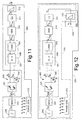
- Figure 11 is a simplified block diagram of a read device of a capacitive sensor in accordance with a third embodiment of the present invention; and
- Figure 12 is a simplified block diagram of an electronic apparatus incorporating the read device illustrated in Figure 11.
- Illustrated in Figure 5 and designated by the
reference number 100 is an apparatus for detecting accelerations, comprising aninertial sensor 101 of a differential capacitive MEMS type, and aread device 103, associated to theinertial sensor 101. The example that will be described hereinafter must not, however, be considered limiting in so far as the invention can be used for reading capacitive sensors of any type. - The
inertial sensor 101, in itself known, comprises a movable body (not illustrated), which is movable with respect to a fixed body (which is not illustrated either) and is capacitively coupled thereto so as to form in practice afirst sense capacitor 102a, and asecond sense capacitor 102b (see for this item Figure 7). The capacitance of thefirst sense capacitor 102a andsecond sense capacitor 102b depend on the relative position of the movable body with respect to the fixed body and vary in a differential way. In practice, thefirst sense capacitor 102a and thesecond sense capacitor 102b have the same rest capacitance CS when theinertial sensor 1 is not subjected to the quantity to be sensed, and show capacitance variations ΔCS of equal amplitude and opposite sign when theinertial sensor 1 senses an acceleration along a predetermined axis. In Figure 5, disturbance caused by theinertial sensor 101 is represented schematically by acurrent generator 150, which injects a disturbance current ID into the input of theread device 103. - The
read device 103 is of the discrete-time type and comprises asignal source 104, amodulator stage 105, asense circuit 107, ademodulator stage 110, and alowpass filter 112. Furthermore, a phase-generator stage 113 generates a plurality of timing signals S1-S6, necessary for co-ordinating operation of the different components of theread device 103. In greater detail, the phase-generator stage 113 comprises anoscillator 113a and a plurality of timing modules C1-C6, controlled by theoscillator 113a, each of which generates a respective timing signal S1-S6. - The
signal source 104 supplies a step read voltage VRD, preferably of an amplitude equal to the maximum dynamics available, which, in the embodiment described, is equal to the supply voltage VDD (for example, 3 V). - The
modulator stage 105 is arranged between thesignal source 104 and theinertial sensor 101 and modulates the read voltage VRD, multiplying it at each read cycle alternately by +1 and -1 (for example, the reading frequency is comprised between 10 and 100 kHz). In practice, a square-wave modulated read voltage VRDM is present on the output of themodulator stage 105 and is supplied to theinertial sensor 101. Reading of theinertial sensor 101 is performed on each edge, both the leading edge and the trailing edge, of the modulated read voltage VRDM. - The
sense circuit 107 comprises a charge-voltage converter 108 and acancelling stage 109. - The charge-
voltage converter 108, of the switched-capacitor type, is set downstream of theinertial sensor 101. In particular, the charge-voltage converter 108 receives a first sense charge QA and a second sense charge QB, which are supplied by theinertial sensor 101 in response to the modulated read voltage VRDM and are correlated to the differential variations of capacitance ΔCS of thefirst sense capacitor 102a and of thesecond sense capacitor 102b. - The
cancelling stage 109 is connected in series to outputs of the charge-voltage converter 108 and is used for cancelling the offset and the low-frequency noise introduced by the charge-voltage converter 108 itself. A modulated output voltage VOM is present between the outputs of thecancelling stage 109. - The
demodulator 110 is cascaded to thecancelling stage 109, for receiving the modulated output voltage VOM, which is again multiplied alternately by +1 and -1 at each read cycle and converted into a demodulated output voltage VOD. - Finally, the
lowpass filter 112 receives the demodulated output voltage VOD, eliminates the high-frequency components, and supplies a corrected output voltage VOC. - The
read device 103 enables suppression also of the disturbance due to theinertial sensor 101, in addition to the low-voltage noise and to the offset introduced by the charge-voltage converter 108. The modulation, in fact, enables separation of the harmonic content of the read voltage VRD and of the variations of capacitance ΔCS from that of the disturbance caused by theinertial sensor 101. In particular, the modulation translates at high frequency the spectrum of the variations of capacitance ΔCS that are linked to the quantities detected by the inertial sensor 101 (i.e., the useful signal, Figures 6a and 6b), whereas the disturbance components, which intervene downstream of the charge-voltage converter 108, remain in base band (Figure 6c, modulated output voltage VOM). The demodulation in practice reverses the content, and hence the useful component, which contains the information on the variations of capacitance ΔCS of theinertial sensor 1, is brought back into the base band, whereas the disturbance component is translated at high frequency (Figure 6d, demodulated output voltage VOD). The disturbance can then readily be eliminated by thelowpass filter 112, provided that the reading frequency is sufficiently high (Figure 6e, corrected output voltage VOC; the harmonic components linked to the disturbance that are suppressed and the transfer function of thelowpass filter 112 are respectively represented by a dashed line and dashed and dotted line). - Figure 7 shows a more detailed circuit implementation of the acceleration-
detection apparatus 100. - The
inertial sensor 101 is represented schematically by thefirst sense capacitor 102a and thesecond sense capacitor 102b, which have a common terminal forming the drivinginput 101c and respective second terminals forming afirst sense terminal 101a and asecond sense terminal 101b. - The
signal source 104 and themodulator stage 105 are formed by a single circuit, hereinafter referred to as modulatedsource 106, comprising aground line 115, set at a ground voltage VGND (0 V), asupply line 116, supplying a supply voltage VDD, and afirst read switch 118a and asecond read switch 118b, respectively controlled by a first timing signal S1 and a second timing signal S2 (the first timing signal S1 and the second timing signal S2 are generated by a first timer module C1 and by a second timer module C2, respectively). More precisely, thefirst read switch 118a and thesecond read switch 118b have a terminal in common connected to the driving terminal 101c of theinertial sensor 101; moreover, thefirst read switch 118a is connected to theground line 115, whereas thesecond read switch 118b is connected to thesupply line 116. - The charge-
voltage converter 108 comprises a fully differential switched-capacitor charge amplifier 120, having afirst integration capacitor 121a connected between a first input and a first (non-inverting) output and asecond integration capacitor 121b connected between a second input and a second (inverting) output. The first input and the second input of thecharge amplifier 120 are connected to thefirst sense terminal 101a and, respectively, to thesecond sense terminal 101b of theinertial sensor 101. Furthermore, the first input and the second input of thecharge amplifier 120 can be selectively connected to areference line 123, supplying a constant reference voltage VREF by afirst reset switch 125a and, respectively, asecond reset switch 125b. A third reset switch is connected between the outputs of thecharge amplifier 120. All the reset switches 125a, 125b, 125c are controlled by one and the same third timing signal S3, generated by a third timer module C3 of the phase-generator stage 113. - The cancelling
stage 109 comprises afirst hold capacitor 122a and asecond hold capacitor 122b, respectively connected in series to the first output and to the second output of thecharge amplifier 109. - The
demodulator stage 110 has afirst input 110a and asecond input 110b and afirst output 110c and asecond output 110d. A first direct-connection switch 127a and a second direct-connection switch 127b are connected between thefirst input 110a and thefirst output 110c and between thesecond input 110b and thesecond output 110d, respectively, and are controlled by a same fourth timing signal S4 generated by a fourth timer module C4. A first crossed-connection switch 127c and a second crossed-connection switch 127d are connected between thefirst input 110a and thesecond output 110d and between thesecond input 110b and thefirst output 110c, respectively, and are controlled by a same fifth timing signal S5 generated by a fifth timer module C5. In particular, the direct-connection switches connection switches inputs outputs demodulator stage 110 is reversed in consecutive read cycles. In other words, if in a read cycle RDK thefirst input 110a is connected to thefirst output 110c and thesecond input 110b is connected to thesecond output 110d, in the immediately ensuing read cycle RDK+1 thefirst input 110a is connected to thesecond output 110d, and thesecond input 110b is connected to thefirst output 110c. In consecutive read cycles RDK, RDK+1, then, the sign of the demodulated output voltage VOD is once equal (multiplication by +1) and once opposite (multiplication by -1) to the sign of the modulated output voltage VOM. - The
first output 110c and thesecond output 110d of thedemodulator stage 110 are moreover selectively connectable to thereference line 123 by a first cancellingswitch 128a and, respectively, a second cancellingswitch 128b, which are controlled by a same sixth timing signal S6, generated by a sixth timer module C6 of the phase-generator stage 113. - Finally, in the embodiment described herein, the
lowpass filter 112 is of a discrete-time analog type and is substantially configured so as to calculate the arithmetic mean of pairs (or in any case an even number) of successive samples of the demodulated output voltage VOD. The corrected output voltage VOC is hence proportional to said arithmetic mean. - Operation of the acceleration-
detection apparatus 100 will be explained hereinafter with reference also to Figures 8a-8g, which represent time plots corresponding to the modulated read voltage VRDM (Figure 8a) and to the timing signals S1-S6 (Figures 8b-8g) during two consecutive read cycles RDK, RIDK+1. By way of reference, Figure 8h illustrates the theoretical evolution of the read voltage VRD, which is not visible in theread device 103 illustrated in Figure 7 because thesignal source 104 and the modulator stage are provided in a single circuit. In each of the read cycles RDK, RDK+1, the steps of reset, offset cancelling, and sensing are designated, respectively, by R, C, and S. Furthermore, it is understood that, when the timing signals S1-S6 assume the logic values "1" and "0", the corresponding switches are in a closing condition and an opening condition, respectively. - Figures 9a-9f show in a simplified way the configuration of the acceleration-
detection apparatus 100 in the various steps of reset, cancelling and sensing of the two read cycles RDK, RDK+1. In particular, only the parts each time used are illustrated. - Throughout the read cycle RDK, the direct-
connection switches demodulator stage 110 are in closed, and the crossed-connection switches - In the reset step of the read cycle RDK, initial levels of d.c. voltage are fixed for the
sense circuit 107. In detail, the switchedsource 106 keeps the driving terminal 101c of theinertial sensor 101 at ground (Figure 9a, where thefirst read switch 118a is closed, whilst thesecond read switch 118b, not illustrated, is open). The reset switches 125a, 125b, 125c are all closed: consequently, theoutputs inertial sensor 101 and the inputs of thecharge amplifier 120 are connected to thereference line 123, whereas the outputs of thecharge amplifier 120 are short-circuited (reset configuration). Also the cancellingswitches outputs demodulator stage 110 and thecapacitors stage 109 to thereference line 123. - In the subsequent cancelling step (Figure 9b), the reset switches 125a, 125b, 125c (not illustrated) are opened, together with the cancelling
switches charge amplifier 120 are stored on thecapacitors stage 109. - A sensing step is then executed (Figure 9c). In detail, the
first read switch 118a and the cancellingswitches second read switch 118b are closed. In this way, the driving terminal 101c of theinertial sensor 101 is connected to thesupply line 116 and thus receives a positive-voltage step having amplitude equal to VDD (indicated schematically in Figure 9c). In response to the positive-voltage step, the output of the cancellingstage 109 supplies a value of the modulated output voltage VOM, correlated to the variations of capacitance ΔCS of theinertial sensor 101, which, however, does not remain constant. In fact, the disturbance current ID (substantially constant) is integrated by thecharge amplifier 120, and its effect is superimposed on the injection of charge of theinertial sensor 101 and causes a drift of the modulated output voltage VOM, with a first sign. Furthermore, the demodulated output voltage VOD is equal both in absolute value and in sign to the modulated output voltage VOM. - The read cycle RDK comes to an end, and the next read cycle RDK+1 is executed. In this case, the modulated
source 106 keeps the driving terminal 101c of theinertial sensor 101 at the supply voltage VDD during the steps of reset and cancelling and supplies a negative-voltage step in the sensing step. - More in detail, in the reset step (Figure 9d) the
second read switch 118b, the reset switches 125a, 125b, 125c, and the cancellingswitches first read switch 118a and (herein not illustrated) are opened. Furthermore, the crossed-connection switches demodulator stage 110 are closed, and the direct-connection switches first input 110a and thesecond input 110b of thedemodulator stage 110 are respectively connected to thesecond output 110d and to thefirst output 110c (in practice, the connection is reversed with respect to the immediately preceding read cycle RDK). Alternatively, switching of the direct-connection switches connection switches - In the subsequent cancelling step (Figure 9e), the reset switches 125a, 125b, 125c (not illustrated) switch, whereas the cancelling
switches hold capacitors stage 109. - In the sensing step (Figure 9f), the
first read switch 118a is closed, whereas thesecond read switch 118b (not illustrated) is opened. Consequently, the modulated read voltage VRDM presents a negative step, having amplitude equal to -VDD. At the reading frequency used, the modulated output voltage VOM on output from the cancellingstage 109 has substantially the same absolute value that it had in the immediately preceding read cycle RDK, but has opposite sign because it is generated in response to a negative-voltage step. The effect of the disturbance current ID is instead identical. Furthermore, thedemodulator stage 110 inverts the connection of thefirst input 110a and of thesecond input 110b with thefirst output 110c and thesecond output 110d, so that the demodulated output voltage VOD has the same absolute value but is of opposite sign with respect to the modulated output voltage VOM. - In practice, owing to the action of the modulated
source 106 and of thedemodulator 110, the effect of the disturbance current ID on the demodulated output voltage VOD has opposite sign in any two consecutive read cycles. Since thelowpass filter 112 executes an arithmetic mean of an even number of samples of the demodulated output voltage VOD, the effect of the disturbance current ID and hence of all the possible dispersions upstream of thecharge amplifier 120 is substantially eliminated. The modulatedsource 106 and the demodulator stage are controlled by timing signals (first, second, fourth, and fifth timing signal S1, S2, S4, S5), which have a period twice that of the ones used for reset and cancelling (third and sixth timing signal S3, S6). In this way, it is possible to invert in sign the correlation between the modulated read voltage VRDM and the demodulated output voltage VOD in consecutive read cycles, which have the same logic sequence of steps. - The device described herein exploits in a particularly advantageous way the characteristics of discrete-time analog circuits, in particular switched-capacitor ones, for carrying out modulation of the read voltage and demodulation of the output voltage. The modulated
source 106 and thedemodulator stage 110 are provided by extremely simple and efficient circuit solutions, since, in practice, switches appropriately controlled by the phase-generator stage 113 are used. The solution described affords considerable advantages also from the standpoints of the speed and of power consumption. - Figure 10 shows a second embodiment of the invention. In this case, an acceleration-
detection apparatus 200 comprises aninertial sensor 201, of the differential capacitive MEMS type, as already described previously, and aread device 203, associated to theinertial sensor 201. Theread device 203, which is of the discrete-time type, comprises asignal source 204, amodulator stage 205, asensing stage 207, which in turn includes a charge-voltage converter 208, a cancellingstage 209, ademodulator stage 210, and a phase-generator stage 213 substantially identical to the ones already described. Furthermore, theread device 203 includes a sigma-delta analog-to-digital converter of a lowpass type, more simply referred to as sigma-delta converter 212, which is connected downstream of thedemodulator stage 210. In this case, the sigma-delta converter 212 advantageously also integrates the function of the lowpass filter and thus suppresses the effects of the disturbance current ID due to the dispersions upstream of the charge-voltage converter 208. The output of the sigma-delta converter 212 generates a corrected numeric acceleration signal AC directly starting from the demodulated output voltage VOD supplied by thedemodulator stage 210. - In accordance with a third embodiment of the invention (illustrated in Figure 11), an acceleration-
detection apparatus 300 comprises aninertial sensor 301 of the differential capacitive MEMS type, as already described previously, and aread device 303, associated to theinertial sensor 301. Theread device 303, of the discrete-time type, comprises asignal source 304, amodulator stage 305, asensing stage 307, which in turn includes a charge-voltage converter 308, a cancellingstage 309, ademodulator stage 310, and a phase-generator stage 313, substantially identical to the ones already described. Furthermore, theread device 303 comprises a sigma-delta converter 311 and alowpass filter 312 of a numeric type, cascaded to one another downstream of thedemodulator stage 310. - The output of the sigma-
delta converter 312 generates a demodulated numeric acceleration signal A starting from the demodulated output voltage VOD, supplied by thedemodulator stage 310. In the demodulated numeric acceleration signal A, there are still present the effects of the disturbance current ID due to the dispersions upstream of the charge-voltage converter 308. - The
lowpass filter 312 receives the demodulated numeric acceleration signal A and calculates a mean value thereof on an even number of samples, for generating a corrected numeric acceleration signal AC. - As illustrated schematically in Figure 12, the
lowpass filter 312 can be advantageously integrated in aprocessing unit 318 of anelectronic device 320 incorporating the acceleration-detection apparatus 300, such as, just to cite a few examples, a cellphone, a portable electronic computer or palm-top computer, a control unit of a hard disk drive or of a pointing peripheral for a computer system. Furthermore, thelowpass filter 312 can be obtained by an appropriately configured microprocessor or, alternatively, by dedicated adder and divider circuits. In the latter case, it is particularly advantageous to execute the mean of the demodulated numeric acceleration signal A on a number of samples equal to a power of two. - Finally, it is evident that modifications and variations may be made to the device and to the read method described, without departing from the scope of the present invention, as defined in the annexed claims. In particular, the signal source and the modulator stage can be provided by separate circuits.
Claims (26)
- A read device of a capacitive sensor comprising:- a signal source (104, C1, C2; 204; 304) supplying a first electrical read signal (VRD) for driving said capacitive sensor (101; 201; 301); and- a discrete-time sense circuit (107; 207; 307), connectable to said capacitive sensor (101; 201; 301), for generating a first electrical output signal (VOM), correlated to capacitance variations (ΔCS) of said capacitive sensor (101; 201; 301), in response to variations of said first electrical read signal (VRD) ;characterized in that it comprises:- a modulator stage (105, 106; 205; 305), associated to said signal source (104, C1, C2; 204; 304), for generating a modulated second electrical read signal (VRDM) on the basis of said first electrical read signal (VRD) and supplying said second electrical read signal (VRDM) to said capacitive sensor (101; 201; 301);- a demodulator stage (110; 210; 310), connected to said sense circuit (107; 207; 307), for demodulating said first electrical output signal (VOM) and generating a demodulated second electrical output signal (VOM); and- a lowpass filtering stage (112; 212; 312), connected to said demodulator stage (110; 210; 310), for generating a filtered third electrical output signal (VOC), on the basis of said second electrical output signal (VOM).
- The device according to Claim 1, wherein said modulator stage (105, 106; 205; 305) is controlled so that said second electrical read signal (VRDM) presents a positive step variation in a first read cycle (RDK) and a negative step variation in a second read cycle (RDK+1) consecutive to said first read cycle (RDK).
- The device according to Claim 2, wherein said signal source (104, C1, C2) and said modulator stage (105) are formed by a single circuit forming a modulated signal source (106).
- The device according to Claim 3, wherein said modulated signal source (106) comprises a first line (115), set at a first voltage (VGND), a second line (116), supplying a second voltage (VDD), a terminal (101c), read connection means (118a, 118b), for selectively connecting said terminal to said ground line (115) and to said supply line (116), and sense timing means (C1, C2) for controlling said read connection means (118a, 118b).
- The device according to Claim 4, wherein said read connection means (118a, 118b) are controlled by said first timing means (C1, C2) so as to connect said terminal (101c) in sequence to said first line (115) and to said second line (116) during said first read cycle (RDK) and so as to connect said terminal (101c) in sequence to said second line (116) and to said first line (115) during said second read cycle (RDK+1).
- The device according to any one of Claims 2-5, comprising reset connection means (125a, 125b, 125c) and reset timing means (C3) for selectively bringing said sense circuit (107; 207; 307) into a reset configuration both during said first read cycle (RDK) and during said second read cycle (RDK+1).
- The device according to any one of Claims 2-6, wherein said demodulator stage (110) comprises a first input (110a) and a second input (110b), a first output (110c) and a second output (110d), direct-connection means (127a, 127b) for selectively connecting said first input (110a) to said first output (110c) and said second input (110b) to said second output (110d), and crossed-connection means (127c, 127d) for selectively connecting said first input (110a) to said second output (110d) and said second input (110b) to said first output (110c).
- The device, wherein said demodulator stage (110) comprises demodulation timing means (C4, C5), controlling said direct connection means (127a, 127b) and said crossed-connection means (127c, 127d) for connecting said first input (110a) to said first output (110c) and said second input (110b) to said second output (110d) during said first read cycle (RDK) and for connecting said first input (110a) to said second output (110d) and said second input (110b) to said first output (110c) during said second read cycle (RDK+1).
- The device according to any one of the preceding claims, wherein said filtering means (112; 212, 312) are configured so as to calculate a mean value of said second electrical output signal (VOD) on a even number of samples.
- The device according to any one of the preceding claims, wherein said filtering means (112) comprise a discrete-time analog filter.
- The device according to any one of Claims 1-9, wherein said filtering means (212) comprise an analog-to-digital converter of a lowpass sigma-delta type.
- The device according to any one of Claims 1-9, wherein said filtering means (312) comprise a numeric filter.
- The device according to any one of the preceding claims, wherein said sense circuit (107; 207; 307) comprises a charge-voltage converter (108; 208; 308).
- The device according to Claim 13, wherein said charge-voltage converter (108) comprises a fully differential switched-capacitor charge amplifier (120).
- The device according to Claim 13 or Claim 14, wherein said sense circuit (107; 207; 307) comprises an offset cancelling stage (109; 209; 309) associated to said charge-voltage converter (108; 208; 308).
- A detecting apparatus comprising a capacitive sensor (101; 201; 301) and a read device (103; 203; 303), associated to said capacitive sensor (101; 201; 301) and made according to any one of the preceding claims.
- The apparatus according to Claim 16, wherein said capacitive sensor (101; 201; 301) is a differential micro-electromechanical sensor.
- The method for reading a capacitive sensor comprising the steps of:- generating a first electrical read signal (VRD) for driving a capacitive sensor (101; 201; 301); and- discrete-time generating a first electrical output signal (VOM) correlated to variations of capacitance (ΔCS) of said capacitive sensor (101; 201; 301), in response to variations of said first electrical read signal (VRD);characterized in that it comprises the steps of:- modulating said electrical read signal (VRD) for generating a modulated second electrical read signal (VRDM);- driving said capacitive sensor (101; 201; 301) by said second electrical read signal (VRDM);- demodulating said first electrical output signal (VOM) for generating a demodulated second electrical output signal (VOD); and- lowpass filtering said second electrical output signal (VOM) for generating a third filtered electrical output signal (VOC).
- The method according to Claim 18, wherein said second electrical read signal (VRDM) presents a positive step variation in a first read cycle (RDK) and a negative step variation in a second read cycle (RDK+1) consecutive to said first read cycle (RDK).
- The method according to Claim 19, wherein said step of modulating comprises:- connecting, during said first read cycle (RDK), a driving terminal (101c) of said capacitive sensor (101) in sequence to a first line (115), set at a first voltage (VGND), and to a second line (116), supplying a second voltage (VDD); and- connecting, during said second read cycle (RDK+1), said driving terminal (101c) in sequence to said second line (116) and to said first line (115).
- The method according to Claim 19, wherein said step of connecting during said first read cycle (RDK) comprises first timing read connection means (118a, 118b), set between said driving terminal (101c), said first line (115), and said second line (116), and said step of connecting during said second read cycle (RDK+1) comprises second timing said read connection means (118a, 118b).
- The method according to any one of Claims 19-21, comprising the steps of:- connecting a sense circuit (107; 207; 307) to said capacitive sensor (101; 201; 301); and- bringing said sense circuit (107; 207; 307) into a reset configuration both during said first read cycle (RDK) and during said second read cycle (RDK+1).
- The method according to any one of Claims 20-22, wherein said demodulating step comprises:- supplying said first electrical output signal (VOM) between a first terminal (110a) and a second terminal (110b);- supplying said second electrical output signal (VOD) between a third terminal (110c) and a fourth terminal (110d);- connecting said first terminal (110a) to said third terminal (110c) and said second terminal (110b) to said fourth terminal (110d) during said first read cycle (RDK); and- connecting said first terminal (110a) to said fourth terminal (110d) and said second terminal (110b) to said third terminal (110c) during said second read cycle (RDK+1).
- The method according to any one of Claims 20-23, wherein said sense circuit (107) comprises a fully differential switched-capacitor charge amplifier (120).
- The method according to any one of Claims 18-24, wherein said step of lowpass filtering comprises calculating a mean value of said second electrical output signal (VOD) on an even number of samples.
- The method according to Claim 25, wherein said step of lowpass filtering comprises executing an analog-to-digital conversion by a sigma-delta converter (212) of a lowpass type.
Priority Applications (5)
| Application Number | Priority Date | Filing Date | Title |
|---|---|---|---|
| DE602005027713T DE602005027713D1 (en) | 2005-12-02 | 2005-12-02 | Device and method for reading a capacitive sensor, in particular a micro-electro-mechanical sensor |
| EP05425863A EP1793497B1 (en) | 2005-12-02 | 2005-12-02 | Device and method for reading a capacitive sensor, in particular of a micro-electromechanical type |
| US11/565,454 US7595648B2 (en) | 2005-12-02 | 2006-11-30 | Device and method for reading a capacitive sensor, in particular of a micro-electromechanical type |
| JP2006326075A JP4805798B2 (en) | 2005-12-02 | 2006-12-01 | Apparatus and method for reading a capacitive sensor in particular of a microelectromechanical type |
| CN200610064336XA CN101033984B (en) | 2005-12-02 | 2006-12-04 | Device and method for reading, in particular, capacitive sensors of the microelectromechanical type |
Applications Claiming Priority (1)
| Application Number | Priority Date | Filing Date | Title |
|---|---|---|---|
| EP05425863A EP1793497B1 (en) | 2005-12-02 | 2005-12-02 | Device and method for reading a capacitive sensor, in particular of a micro-electromechanical type |
Publications (2)
| Publication Number | Publication Date |
|---|---|
| EP1793497A1 true EP1793497A1 (en) | 2007-06-06 |
| EP1793497B1 EP1793497B1 (en) | 2011-04-27 |
Family
ID=36218104
Family Applications (1)
| Application Number | Title | Priority Date | Filing Date |
|---|---|---|---|
| EP05425863A Expired - Lifetime EP1793497B1 (en) | 2005-12-02 | 2005-12-02 | Device and method for reading a capacitive sensor, in particular of a micro-electromechanical type |
Country Status (5)
| Country | Link |
|---|---|
| US (1) | US7595648B2 (en) |
| EP (1) | EP1793497B1 (en) |
| JP (1) | JP4805798B2 (en) |
| CN (1) | CN101033984B (en) |
| DE (1) | DE602005027713D1 (en) |
Families Citing this family (57)
| Publication number | Priority date | Publication date | Assignee | Title |
|---|---|---|---|---|
| US7385443B1 (en) | 2007-01-31 | 2008-06-10 | Medtronic, Inc. | Chopper-stabilized instrumentation amplifier |
| US7391257B1 (en) * | 2007-01-31 | 2008-06-24 | Medtronic, Inc. | Chopper-stabilized instrumentation amplifier for impedance measurement |
| US8265769B2 (en) | 2007-01-31 | 2012-09-11 | Medtronic, Inc. | Chopper-stabilized instrumentation amplifier for wireless telemetry |
| US9615744B2 (en) * | 2007-01-31 | 2017-04-11 | Medtronic, Inc. | Chopper-stabilized instrumentation amplifier for impedance measurement |
| US8106668B2 (en) * | 2007-04-24 | 2012-01-31 | Seiko Instruments Inc. | Proximity detector and proximity detecting method |
| US8781595B2 (en) | 2007-04-30 | 2014-07-15 | Medtronic, Inc. | Chopper mixer telemetry circuit |
| KR100915149B1 (en) * | 2007-07-19 | 2009-09-03 | (주)에스엠엘전자 | Multi-channel capacitive sensing circuit |
| US7786738B2 (en) * | 2007-09-19 | 2010-08-31 | Robert Bosch Gmbh | Cancelling low frequency errors in MEMS systems |
| US8380314B2 (en) | 2007-09-26 | 2013-02-19 | Medtronic, Inc. | Patient directed therapy control |
| WO2009070814A2 (en) * | 2007-11-27 | 2009-06-04 | Frederick Johannes Bruwer | Capacitive sensing circuit with noise rejection |
| US9072870B2 (en) | 2008-01-25 | 2015-07-07 | Medtronic, Inc. | Sleep stage detection |
| DE102008023535B4 (en) * | 2008-05-14 | 2011-05-12 | Texas Instruments Deutschland Gmbh | Electronic device and method for evaluating a variable capacity |
| US8478402B2 (en) * | 2008-10-31 | 2013-07-02 | Medtronic, Inc. | Determining intercardiac impedance |
| US8104346B2 (en) * | 2008-11-10 | 2012-01-31 | Westerngeco L.L.C. | MEMS-based capacitive sensor |
| IT1392553B1 (en) | 2008-12-11 | 2012-03-09 | St Microelectronics Rousset | ELECTRONIC DEVICE WITH VARIABLE CAPACITY AND MICROELETTROMECHANICAL DEVICE INCORPORATING SUCH ELECTRONIC DEVICE |
| US7969167B2 (en) * | 2009-01-28 | 2011-06-28 | Freescale Semiconductor, Inc. | Capacitance-to-voltage interface circuit with shared capacitor bank for offsetting and analog-to-digital conversion |
| US9770204B2 (en) | 2009-11-11 | 2017-09-26 | Medtronic, Inc. | Deep brain stimulation for sleep and movement disorders |
| US8714012B2 (en) * | 2010-02-16 | 2014-05-06 | Stmicroelectronics S.R.L. | Microelectromechanical gyroscope with inversion of actuation forces, and method for actuating a microelectromechanical gyroscope |
| WO2011138530A1 (en) * | 2010-05-07 | 2011-11-10 | Stmicroelectronics (Rousset) Sas | Method and device for characterizing or measuring a floating capacitor |
| US9278845B2 (en) | 2010-09-18 | 2016-03-08 | Fairchild Semiconductor Corporation | MEMS multi-axis gyroscope Z-axis electrode structure |
| DE112011103124B4 (en) | 2010-09-18 | 2025-10-30 | Fairchild Semiconductor Corporation | Bending bearings for reducing quadrature in oscillating micromechanical devices |
| US9455354B2 (en) | 2010-09-18 | 2016-09-27 | Fairchild Semiconductor Corporation | Micromachined 3-axis accelerometer with a single proof-mass |
| EP2616771B8 (en) | 2010-09-18 | 2018-12-19 | Fairchild Semiconductor Corporation | Micromachined monolithic 6-axis inertial sensor |
| KR101871865B1 (en) | 2010-09-18 | 2018-08-02 | 페어차일드 세미컨덕터 코포레이션 | Multi-die mems package |
| US9156673B2 (en) | 2010-09-18 | 2015-10-13 | Fairchild Semiconductor Corporation | Packaging to reduce stress on microelectromechanical systems |
| US9006846B2 (en) | 2010-09-20 | 2015-04-14 | Fairchild Semiconductor Corporation | Through silicon via with reduced shunt capacitance |
| KR101332701B1 (en) | 2010-09-20 | 2013-11-25 | 페어차일드 세미컨덕터 코포레이션 | Microelectromechanical pressure sensor including reference capacitor |
| US9217805B2 (en) | 2010-10-01 | 2015-12-22 | Westerngeco L.L.C. | Monitoring the quality of particle motion data during a seismic acquisition |
| US9525925B2 (en) * | 2011-02-25 | 2016-12-20 | Infineon Technologies Ag | Sensor with movable part and biasing |
| EP2792069B1 (en) * | 2011-12-16 | 2016-11-02 | Analog Devices, Inc. | Low noise amplifier for multiple channels |
| US9062972B2 (en) | 2012-01-31 | 2015-06-23 | Fairchild Semiconductor Corporation | MEMS multi-axis accelerometer electrode structure |
| US8978475B2 (en) | 2012-02-01 | 2015-03-17 | Fairchild Semiconductor Corporation | MEMS proof mass with split z-axis portions |
| US8742964B2 (en) * | 2012-04-04 | 2014-06-03 | Fairchild Semiconductor Corporation | Noise reduction method with chopping for a merged MEMS accelerometer sensor |
| US9488693B2 (en) | 2012-04-04 | 2016-11-08 | Fairchild Semiconductor Corporation | Self test of MEMS accelerometer with ASICS integrated capacitors |
| KR102058489B1 (en) | 2012-04-05 | 2019-12-23 | 페어차일드 세미컨덕터 코포레이션 | Mems device front-end charge amplifier |
| US9069006B2 (en) | 2012-04-05 | 2015-06-30 | Fairchild Semiconductor Corporation | Self test of MEMS gyroscope with ASICs integrated capacitors |
| EP2647952B1 (en) | 2012-04-05 | 2017-11-15 | Fairchild Semiconductor Corporation | Mems device automatic-gain control loop for mechanical amplitude drive |
| EP2647955B8 (en) | 2012-04-05 | 2018-12-19 | Fairchild Semiconductor Corporation | MEMS device quadrature phase shift cancellation |
| US9625272B2 (en) | 2012-04-12 | 2017-04-18 | Fairchild Semiconductor Corporation | MEMS quadrature cancellation and signal demodulation |
| US9094027B2 (en) | 2012-04-12 | 2015-07-28 | Fairchild Semiconductor Corporation | Micro-electro-mechanical-system (MEMS) driver |
| DE102013014881B4 (en) | 2012-09-12 | 2023-05-04 | Fairchild Semiconductor Corporation | Enhanced silicon via with multi-material fill |
| ITTO20121116A1 (en) * | 2012-12-20 | 2014-06-21 | St Microelectronics Srl | CIRCUIT AND DYNAMIC COMPENSATION METHOD OF OFFSET FOR A MEMS SENSOR DEVICE |
| US9459274B2 (en) * | 2013-03-13 | 2016-10-04 | Invensense, Inc. | Round-robin sensing device and method of use |
| US9835647B2 (en) | 2014-03-18 | 2017-12-05 | Fairchild Semiconductor Corporation | Apparatus and method for extending analog front end sense range of a high-Q MEMS sensor |
| US9924904B2 (en) | 2014-09-02 | 2018-03-27 | Medtronic, Inc. | Power-efficient chopper amplifier |
| EP3236585B1 (en) * | 2016-04-22 | 2020-12-23 | Goodix Technology (HK) Company Limited | Amplifiers |
| DE102016109114B4 (en) | 2016-05-18 | 2025-06-18 | Infineon Technologies Ag | Level converter circuit, as well as measuring arrangement and chip with such a level converter circuit |
| DE102016109118A1 (en) * | 2016-05-18 | 2017-11-23 | Infineon Technologies Ag | Circuit architecture for a measuring device, a level converter circuit, a charge pumping stage and a charge pump and method for operating these |
| JP6733381B2 (en) | 2016-07-15 | 2020-07-29 | セイコーエプソン株式会社 | Physical quantity detection circuit, physical quantity detection device, electronic device and moving body |
| IT201600103234A1 (en) | 2016-10-14 | 2018-04-14 | Green Seas Ventures Ldt | Constructive system relating to a capacitive voltage sensor |
| CN106526230B (en) * | 2016-12-19 | 2019-10-15 | 兰州空间技术物理研究所 | Method and device for improving wide-band dynamic measurement capability of quartz flexible accelerometer |
| IT201800004114A1 (en) | 2018-03-30 | 2019-09-30 | Green Seas Ventures Ltd C/O Citco B V I Ltd | CONSTRUCTION SYSTEM WITH A CAPACITIVE VOLTAGE SENSOR |
| CN113227802B (en) | 2018-12-17 | 2025-02-11 | G&W电气公司 | Electrical sensor assembly |
| EP3899553A4 (en) | 2018-12-17 | 2022-10-26 | G & W Electric Company | ELECTRICAL SENSOR ARRANGEMENT |
| US11984860B2 (en) | 2021-06-23 | 2024-05-14 | Stmicroelectronics S.R.L. | Charge amplification circuits and methods |
| TWI843238B (en) * | 2022-10-19 | 2024-05-21 | 財團法人工業技術研究院 | Reading device for capacitive sensing element |
| FR3141300B1 (en) * | 2022-10-20 | 2024-11-08 | Commissariat Energie Atomique | Resonant MEMS sensor suitable for generating a pulsed output signal |
Citations (4)
| Publication number | Priority date | Publication date | Assignee | Title |
|---|---|---|---|---|
| US5343156A (en) * | 1992-04-15 | 1994-08-30 | Nat Semiconductor Corp | IC for producing an output voltage related to fuel composition in a capacitive fuel sensor |
| US5637798A (en) * | 1994-11-03 | 1997-06-10 | Robert Bosch Gmbh | Circuit arrangement for evaluating an acceleration sensor signal |
| JPH10111207A (en) * | 1996-10-08 | 1998-04-28 | Denso Corp | Capacitive pressure sensor |
| US5808198A (en) * | 1997-05-19 | 1998-09-15 | The Charles Stark Draper Laboratory, Inc. | RF balanced capacitive vibration sensor system |
Family Cites Families (20)
| Publication number | Priority date | Publication date | Assignee | Title |
|---|---|---|---|---|
| US3879660A (en) * | 1973-10-24 | 1975-04-22 | John S Piso | Capacitive measuring system |
| US4208625A (en) * | 1976-02-23 | 1980-06-17 | Micro Sensors, Inc. | Capacitive measuring system with automatic calibration |
| JPH0672901B2 (en) * | 1985-11-22 | 1994-09-14 | 日東工器株式会社 | Capacitance-voltage conversion circuit |
| US5801307A (en) * | 1995-07-12 | 1998-09-01 | Netzer; Yishay | Differential windshield capacitive moisture sensors |
| JP3379388B2 (en) * | 1997-06-09 | 2003-02-24 | 株式会社豊田中央研究所 | Capacitance detection circuit |
| JP2000234939A (en) * | 1998-12-18 | 2000-08-29 | Yazaki Corp | Capacitance-voltage converter |
| US6388453B1 (en) * | 1999-01-25 | 2002-05-14 | Bryan D. Greer | Swept-frequency dielectric moisture and density sensor |
| JP2003511684A (en) * | 1999-10-13 | 2003-03-25 | アナログ デバイシーズ インコーポレイテッド | Feedback mechanism for rate gyroscope |
| DE10031522B9 (en) * | 2000-06-28 | 2007-07-12 | Infineon Technologies Ag | Frequency-compensated amplifier arrangement and method for operating a frequency-compensated amplifier arrangement |
| EP1207371B1 (en) * | 2000-11-16 | 2007-01-10 | STMicroelectronics S.r.l. | Automatic calibration of a micro-mechanical sensor |
| DE10107547A1 (en) * | 2001-02-17 | 2002-08-29 | Bosch Gmbh Robert | Method and device for synchronous modulation of multiply modulated signals |
| ITTO20010157A1 (en) * | 2001-02-21 | 2002-08-21 | St Microelectronics Srl | METHOD AND CIRCUIT FOR DETECTION OF MOVEMENTS THROUGH MICRO-ELECTRO-MECHANICAL SENSORS WITH COMPENSATION OF PARASITIC CAPACITY AND MOVEMENT |
| JP4031215B2 (en) * | 2001-06-19 | 2008-01-09 | 株式会社山武 | Sensor signal processing circuit |
| US20030048036A1 (en) * | 2001-08-31 | 2003-03-13 | Lemkin Mark Alan | MEMS comb-finger actuator |
| US20030098699A1 (en) * | 2001-11-16 | 2003-05-29 | Lemkin Mark A. | Sense interface system with velocity feed-through rejection |
| WO2005068959A2 (en) * | 2004-01-05 | 2005-07-28 | Case Western Reserve University | High performance integrated electronic for mems capacitive strain sensors |
| JP2005295517A (en) * | 2004-03-08 | 2005-10-20 | Matsushita Electric Ind Co Ltd | Mixer circuit and receiving circuit using mixer circuit |
| US7134336B2 (en) * | 2004-03-19 | 2006-11-14 | Denso Corporation | Vibration type angular velocity sensor |
| US7078916B2 (en) * | 2004-04-06 | 2006-07-18 | Analog Devices, Inc. | Linearity enhancement for capacitive sensors |
| US6970126B1 (en) * | 2004-06-25 | 2005-11-29 | Analog Devices, Inc. | Variable capacitance switched capacitor input system and method |
-
2005
- 2005-12-02 EP EP05425863A patent/EP1793497B1/en not_active Expired - Lifetime
- 2005-12-02 DE DE602005027713T patent/DE602005027713D1/en not_active Expired - Lifetime
-
2006
- 2006-11-30 US US11/565,454 patent/US7595648B2/en active Active
- 2006-12-01 JP JP2006326075A patent/JP4805798B2/en not_active Expired - Fee Related
- 2006-12-04 CN CN200610064336XA patent/CN101033984B/en active Active
Patent Citations (4)
| Publication number | Priority date | Publication date | Assignee | Title |
|---|---|---|---|---|
| US5343156A (en) * | 1992-04-15 | 1994-08-30 | Nat Semiconductor Corp | IC for producing an output voltage related to fuel composition in a capacitive fuel sensor |
| US5637798A (en) * | 1994-11-03 | 1997-06-10 | Robert Bosch Gmbh | Circuit arrangement for evaluating an acceleration sensor signal |
| JPH10111207A (en) * | 1996-10-08 | 1998-04-28 | Denso Corp | Capacitive pressure sensor |
| US5808198A (en) * | 1997-05-19 | 1998-09-15 | The Charles Stark Draper Laboratory, Inc. | RF balanced capacitive vibration sensor system |
Non-Patent Citations (1)
| Title |
|---|
| PATENT ABSTRACTS OF JAPAN vol. 1998, no. 09 31 July 1998 (1998-07-31) * |
Also Published As
| Publication number | Publication date |
|---|---|
| CN101033984A (en) | 2007-09-12 |
| JP4805798B2 (en) | 2011-11-02 |
| EP1793497B1 (en) | 2011-04-27 |
| CN101033984B (en) | 2011-01-12 |
| US7595648B2 (en) | 2009-09-29 |
| JP2007155729A (en) | 2007-06-21 |
| DE602005027713D1 (en) | 2011-06-09 |
| US20070152682A1 (en) | 2007-07-05 |
Similar Documents
| Publication | Publication Date | Title |
|---|---|---|
| EP1793497B1 (en) | Device and method for reading a capacitive sensor, in particular of a micro-electromechanical type | |
| JP4352562B2 (en) | Signal processing device | |
| JP2561040B2 (en) | Capacitance sensor capacitance change detection circuit and detection method thereof | |
| WO2008008403A2 (en) | Signal conditioning methods and circuits for a capacitive sensing integrated tire pressure sensor | |
| US9329724B2 (en) | Signal processing circuit for touch screen and method for controlling the same | |
| US6952966B2 (en) | Apparatus for detecting physical quantity | |
| CN104048656A (en) | Round-robin sensing device and method of use | |
| JP5341745B2 (en) | Magnetic detector | |
| JP2011107086A (en) | Capacitance detection circuit, pressure detector, acceleration detector and transducer for microphone | |
| US20030098699A1 (en) | Sense interface system with velocity feed-through rejection | |
| US10914583B2 (en) | Sense amplifiers for gyroscopes and related systems and methods | |
| JP2012037439A (en) | Electrostatic capacitance detection circuit | |
| KR100450165B1 (en) | Voltage comparing circuit | |
| JPH08327677A (en) | Capacitive sensor detection circuit and detection method | |
| US10585539B2 (en) | High sensitivity readout circuit for touch panel | |
| JP2005140657A (en) | Capacitance sensor capacitance change detection circuit | |
| CN211787048U (en) | Integrator, touch capacitance detection circuit and intelligent device | |
| CN113287027B (en) | Capacitance detection circuit, touch device, terminal equipment and capacitance detection method | |
| KR101354782B1 (en) | Detecting appartus for gyro sensor signal and method thereof | |
| JP4269388B2 (en) | Capacitive physical quantity detector | |
| JP3379388B2 (en) | Capacitance detection circuit | |
| JP2004347493A (en) | Capacitive sensor device with abnormality detection function | |
| JP2005233626A (en) | Wheel speed detecting apparatus | |
| CN111510143A (en) | Front-end circuit for direct conversion from capacitance to digital quantity | |
| CN101888238B (en) | Capacitor interface circuit |
Legal Events
| Date | Code | Title | Description |
|---|---|---|---|
| PUAI | Public reference made under article 153(3) epc to a published international application that has entered the european phase |
Free format text: ORIGINAL CODE: 0009012 |
|
| AK | Designated contracting states |
Kind code of ref document: A1 Designated state(s): AT BE BG CH CY CZ DE DK EE ES FI FR GB GR HU IE IS IT LI LT LU LV MC NL PL PT RO SE SI SK TR |
|
| AX | Request for extension of the european patent |
Extension state: AL BA HR MK YU |
|
| 17P | Request for examination filed |
Effective date: 20071203 |
|
| 17Q | First examination report despatched |
Effective date: 20080108 |
|
| AKX | Designation fees paid |
Designated state(s): DE FR GB IT |
|
| RAP1 | Party data changed (applicant data changed or rights of an application transferred) |
Owner name: STMICROELECTRONICS SRL |
|
| GRAP | Despatch of communication of intention to grant a patent |
Free format text: ORIGINAL CODE: EPIDOSNIGR1 |
|
| GRAS | Grant fee paid |
Free format text: ORIGINAL CODE: EPIDOSNIGR3 |
|
| GRAA | (expected) grant |
Free format text: ORIGINAL CODE: 0009210 |
|
| AK | Designated contracting states |
Kind code of ref document: B1 Designated state(s): DE FR GB IT |
|
| REG | Reference to a national code |
Ref country code: GB Ref legal event code: FG4D |
|
| REF | Corresponds to: |
Ref document number: 602005027713 Country of ref document: DE Date of ref document: 20110609 Kind code of ref document: P |
|
| REG | Reference to a national code |
Ref country code: DE Ref legal event code: R096 Ref document number: 602005027713 Country of ref document: DE Effective date: 20110609 |
|
| PLBE | No opposition filed within time limit |
Free format text: ORIGINAL CODE: 0009261 |
|
| STAA | Information on the status of an ep patent application or granted ep patent |
Free format text: STATUS: NO OPPOSITION FILED WITHIN TIME LIMIT |
|
| 26N | No opposition filed |
Effective date: 20120130 |
|
| REG | Reference to a national code |
Ref country code: DE Ref legal event code: R097 Ref document number: 602005027713 Country of ref document: DE Effective date: 20120130 |
|
| PGFP | Annual fee paid to national office [announced via postgrant information from national office to epo] |
Ref country code: GB Payment date: 20131125 Year of fee payment: 9 |
|
| PGFP | Annual fee paid to national office [announced via postgrant information from national office to epo] |
Ref country code: IT Payment date: 20131122 Year of fee payment: 9 |
|
| PGFP | Annual fee paid to national office [announced via postgrant information from national office to epo] |
Ref country code: FR Payment date: 20131219 Year of fee payment: 9 |
|
| GBPC | Gb: european patent ceased through non-payment of renewal fee |
Effective date: 20141202 |
|
| REG | Reference to a national code |
Ref country code: FR Ref legal event code: ST Effective date: 20150831 |
|
| PG25 | Lapsed in a contracting state [announced via postgrant information from national office to epo] |
Ref country code: GB Free format text: LAPSE BECAUSE OF NON-PAYMENT OF DUE FEES Effective date: 20141202 |
|
| PG25 | Lapsed in a contracting state [announced via postgrant information from national office to epo] |
Ref country code: FR Free format text: LAPSE BECAUSE OF NON-PAYMENT OF DUE FEES Effective date: 20141231 |
|
| PG25 | Lapsed in a contracting state [announced via postgrant information from national office to epo] |
Ref country code: IT Free format text: LAPSE BECAUSE OF NON-PAYMENT OF DUE FEES Effective date: 20141202 |
|
| REG | Reference to a national code |
Ref country code: DE Ref legal event code: R082 Ref document number: 602005027713 Country of ref document: DE Representative=s name: SCHMITT-NILSON SCHRAUD WAIBEL WOHLFROM PATENTA, DE |
|
| PGFP | Annual fee paid to national office [announced via postgrant information from national office to epo] |
Ref country code: DE Payment date: 20241121 Year of fee payment: 20 |
|
| REG | Reference to a national code |
Ref country code: DE Ref legal event code: R071 Ref document number: 602005027713 Country of ref document: DE |