JP6733381B2 - Physical quantity detection circuit, physical quantity detection device, electronic device and moving body - Google Patents
Physical quantity detection circuit, physical quantity detection device, electronic device and moving body Download PDFInfo
- Publication number
- JP6733381B2 JP6733381B2 JP2016140347A JP2016140347A JP6733381B2 JP 6733381 B2 JP6733381 B2 JP 6733381B2 JP 2016140347 A JP2016140347 A JP 2016140347A JP 2016140347 A JP2016140347 A JP 2016140347A JP 6733381 B2 JP6733381 B2 JP 6733381B2
- Authority
- JP
- Japan
- Prior art keywords
- circuit
- signal
- physical quantity
- quantity detection
- output
- Prior art date
- Legal status (The legal status is an assumption and is not a legal conclusion. Google has not performed a legal analysis and makes no representation as to the accuracy of the status listed.)
- Active
Links
Images


Classifications
-
- H—ELECTRICITY
- H03—ELECTRONIC CIRCUITRY
- H03F—AMPLIFIERS
- H03F3/00—Amplifiers with only discharge tubes or only semiconductor devices as amplifying elements
- H03F3/38—Dc amplifiers with modulator at input and demodulator at output; Modulators or demodulators specially adapted for use in such amplifiers
- H03F3/387—Dc amplifiers with modulator at input and demodulator at output; Modulators or demodulators specially adapted for use in such amplifiers with semiconductor devices only
-
- G—PHYSICS
- G01—MEASURING; TESTING
- G01D—MEASURING NOT SPECIALLY ADAPTED FOR A SPECIFIC VARIABLE; ARRANGEMENTS FOR MEASURING TWO OR MORE VARIABLES NOT COVERED IN A SINGLE OTHER SUBCLASS; TARIFF METERING APPARATUS; MEASURING OR TESTING NOT OTHERWISE PROVIDED FOR
- G01D21/00—Measuring or testing not otherwise provided for
-
- G—PHYSICS
- G01—MEASURING; TESTING
- G01D—MEASURING NOT SPECIALLY ADAPTED FOR A SPECIFIC VARIABLE; ARRANGEMENTS FOR MEASURING TWO OR MORE VARIABLES NOT COVERED IN A SINGLE OTHER SUBCLASS; TARIFF METERING APPARATUS; MEASURING OR TESTING NOT OTHERWISE PROVIDED FOR
- G01D5/00—Mechanical means for transferring the output of a sensing member; Means for converting the output of a sensing member to another variable where the form or nature of the sensing member does not constrain the means for converting; Transducers not specially adapted for a specific variable
- G01D5/12—Mechanical means for transferring the output of a sensing member; Means for converting the output of a sensing member to another variable where the form or nature of the sensing member does not constrain the means for converting; Transducers not specially adapted for a specific variable using electric or magnetic means
- G01D5/14—Mechanical means for transferring the output of a sensing member; Means for converting the output of a sensing member to another variable where the form or nature of the sensing member does not constrain the means for converting; Transducers not specially adapted for a specific variable using electric or magnetic means influencing the magnitude of a current or voltage
- G01D5/24—Mechanical means for transferring the output of a sensing member; Means for converting the output of a sensing member to another variable where the form or nature of the sensing member does not constrain the means for converting; Transducers not specially adapted for a specific variable using electric or magnetic means influencing the magnitude of a current or voltage by varying capacitance
- G01D5/241—Mechanical means for transferring the output of a sensing member; Means for converting the output of a sensing member to another variable where the form or nature of the sensing member does not constrain the means for converting; Transducers not specially adapted for a specific variable using electric or magnetic means influencing the magnitude of a current or voltage by varying capacitance by relative movement of capacitor electrodes
- G01D5/2417—Mechanical means for transferring the output of a sensing member; Means for converting the output of a sensing member to another variable where the form or nature of the sensing member does not constrain the means for converting; Transducers not specially adapted for a specific variable using electric or magnetic means influencing the magnitude of a current or voltage by varying capacitance by relative movement of capacitor electrodes by varying separation
-
- G—PHYSICS
- G11—INFORMATION STORAGE
- G11C—STATIC STORES
- G11C27/00—Electric analogue stores, e.g. for storing instantaneous values
- G11C27/02—Sample-and-hold arrangements
-
- G—PHYSICS
- G11—INFORMATION STORAGE
- G11C—STATIC STORES
- G11C27/00—Electric analogue stores, e.g. for storing instantaneous values
- G11C27/02—Sample-and-hold arrangements
- G11C27/024—Sample-and-hold arrangements using a capacitive memory element
- G11C27/026—Sample-and-hold arrangements using a capacitive memory element associated with an amplifier
-
- H—ELECTRICITY
- H03—ELECTRONIC CIRCUITRY
- H03F—AMPLIFIERS
- H03F3/00—Amplifiers with only discharge tubes or only semiconductor devices as amplifying elements
- H03F3/45—Differential amplifiers
- H03F3/45071—Differential amplifiers with semiconductor devices only
- H03F3/45076—Differential amplifiers with semiconductor devices only characterised by the way of implementation of the active amplifying circuit in the differential amplifier
- H03F3/45475—Differential amplifiers with semiconductor devices only characterised by the way of implementation of the active amplifying circuit in the differential amplifier using IC blocks as the active amplifying circuit
-
- H—ELECTRICITY
- H03—ELECTRONIC CIRCUITRY
- H03G—CONTROL OF AMPLIFICATION
- H03G1/00—Details of arrangements for controlling amplification
- H03G1/0005—Circuits characterised by the type of controlling devices operated by a controlling current or voltage signal
- H03G1/0088—Circuits characterised by the type of controlling devices operated by a controlling current or voltage signal using discontinuously variable devices, e.g. switch-operated
- H03G1/0094—Circuits characterised by the type of controlling devices operated by a controlling current or voltage signal using discontinuously variable devices, e.g. switch-operated using switched capacitors
-
- H—ELECTRICITY
- H03—ELECTRONIC CIRCUITRY
- H03G—CONTROL OF AMPLIFICATION
- H03G3/00—Gain control in amplifiers or frequency changers without distortion of the input signal
- H03G3/001—Digital control of analog signals
-
- H—ELECTRICITY
- H03—ELECTRONIC CIRCUITRY
- H03G—CONTROL OF AMPLIFICATION
- H03G3/00—Gain control in amplifiers or frequency changers without distortion of the input signal
- H03G3/20—Automatic control
-
- H—ELECTRICITY
- H03—ELECTRONIC CIRCUITRY
- H03H—IMPEDANCE NETWORKS, e.g. RESONANT CIRCUITS; RESONATORS
- H03H7/00—Multiple-port networks comprising only passive electrical elements as network components
- H03H7/01—Frequency selective two-port networks
- H03H7/0138—Electrical filters or coupling circuits
-
- H—ELECTRICITY
- H03—ELECTRONIC CIRCUITRY
- H03F—AMPLIFIERS
- H03F2203/00—Indexing scheme relating to amplifiers with only discharge tubes or only semiconductor devices as amplifying elements covered by H03F3/00
- H03F2203/45—Indexing scheme relating to differential amplifiers
- H03F2203/45514—Indexing scheme relating to differential amplifiers the FBC comprising one or more switched capacitors, and being coupled between the LC and the IC
-
- H—ELECTRICITY
- H03—ELECTRONIC CIRCUITRY
- H03H—IMPEDANCE NETWORKS, e.g. RESONANT CIRCUITS; RESONATORS
- H03H19/00—Networks using time-varying elements, e.g. N-path filters
- H03H19/004—Switched capacitor networks
Description
本発明は、物理量検出回路、物理量検出装置、電子機器及び移動体に関する。 The present invention relates to a physical quantity detection circuit, a physical quantity detection device, an electronic device, and a moving body.
現在、様々なシステムや電子機器において、加速度を検出する加速度センサーや角速度を検出するジャイロセンサー等、種々の物理量を検出可能な物理量検出装置が広く利用されている。例えば、特許文献1には、差動容量型センサーに、QVアンプ、プログラマブルゲインアンプ(PGA)及びアナログ−デジタル変換器(ADC)を備えた物理量検出回路を接続して構成される物理量検出装置が開示されている。
Currently, in various systems and electronic devices, a physical quantity detection device capable of detecting various physical quantities such as an acceleration sensor that detects acceleration and a gyro sensor that detects angular velocity is widely used. For example,
特許文献1に記載の物理量検出装置のように、物理量検出素子が出力するアナログ信号に対してアナログ処理を行った後、ADCを用いてデジタル信号に変換する物理量検出装置では、物理量検出素子の駆動周波数とADCのサンプリング周波数を一致させるか、もしくは駆動周波数によるサンプルホールド回路でDC信号に変換する必要がある。駆動周波数とADCのサンプリング周波数を一致させる場合にはアンチエイリアスフィルターを設けることが出来ないため、ADCでのサンプリングによって発生する折り返しノイズにより、低ノイズ化が難しい。また、ADCの前段にサンプルホールド回路とアンチエイリアスフィルターを設けた場合にはサンプルホールド回路による折り返しノイズが発生する。また、アンチエイリアスフィルターは回路速度と回路面積の点で大きくすることが出来ず、低ノイズ化が難しい。
As in the physical quantity detection device described in
本発明は、以上のような問題点に鑑みてなされたものであり、本発明のいくつかの態様によれば、サンプルホールド回路とスイッチトキャパシターフィルター回路を用いた低ノイズ化が可能な物理量検出回路及び物理量検出装置を提供することができる。また、本発明のいくつかの態様によれば、当該物理量検出装置を用いた電子機器及び移動体を提供することができる。 The present invention has been made in view of the above problems, and according to some aspects of the present invention, a physical quantity detection circuit capable of reducing noise using a sample hold circuit and a switched capacitor filter circuit. And a physical quantity detection device can be provided. Further, according to some aspects of the present invention, it is possible to provide an electronic device and a moving body using the physical quantity detection device.
本発明は前述の課題の少なくとも一部を解決するためになされたものであり、以下の態様または適用例として実現することが可能である。 The present invention has been made to solve at least a part of the problems described above, and can be realized as the following aspects or application examples.
[適用例1]
本適用例に係る物理量検出回路は、物理量検出素子の出力信号に基づく第1の信号をサンプルホールドする第1のサンプルホールド回路と、前記第1のサンプルホールド回路の出力信号が入力される増幅回路と、前記増幅回路の第1の出力信号が入力される第1のスイッチトキャパシター回路と、を有し、前記第1のスイッチトキャパシター回路の出力信号が前記増幅回路に入力される、スイッチトキャパシターフィルター回路と、前記スイッチトキャパシターフィルター回路の出力信号をA/D変換するA/D変換回路と、を含む。
[Application example 1]
A physical quantity detection circuit according to this application example includes a first sample hold circuit for sampling and holding a first signal based on an output signal of a physical quantity detection element, and an amplifier circuit to which an output signal of the first sample hold circuit is input. And a first switched capacitor circuit to which the first output signal of the amplifier circuit is input, and the output signal of the first switched capacitor circuit is input to the amplifier circuit. And an A/D conversion circuit for A/D converting the output signal of the switched capacitor filter circuit.
本適用例に係る物理量検出回路では、スイッチトキャパシターフィルター回路は、第1
のスイッチトキャパシター回路によってA/D変換回路の前段のアンチエイリアスフィルターとして機能する。また、第1のサンプルホールド回路によってスイッチトキャパシターフィルター回路の出力信号はDCに近い信号となるため、A/D変換回路によるサンプリングタイミングの自由度が高い。従って、本適用例に係る物理量検出回路によれば、A/D変換回路がスイッチトキャパシターフィルター回路の出力信号をサンプリングする周波数を変えずに物理量検出素子を駆動する周波数を高めることが可能であり、低ノイズ化が可能である。
In the physical quantity detection circuit according to this application example, the switched capacitor filter circuit includes the first
It functions as an anti-aliasing filter in the preceding stage of the A/D conversion circuit by the switched capacitor circuit of. Further, since the output signal of the switched capacitor filter circuit becomes a signal close to DC by the first sample hold circuit, the flexibility of the sampling timing by the A/D conversion circuit is high. Therefore, according to the physical quantity detection circuit of this application example, it is possible to increase the frequency for driving the physical quantity detection element without changing the frequency at which the A/D conversion circuit samples the output signal of the switched capacitor filter circuit, Low noise is possible.
[適用例2]
上記適用例に係る物理量検出回路において、前記増幅回路は、前記第1のサンプルホールド回路の出力信号が入力される第1のチョッピング回路と、前記第1のチョッピング回路の出力信号が入力される演算増幅器と、前記演算増幅器の出力信号が入力される第2のチョッピング回路と、を有してもよい。
[Application example 2]
In the physical quantity detection circuit according to the application example described above, the amplification circuit includes a first chopping circuit to which the output signal of the first sample and hold circuit is input and an operation to which the output signal of the first chopping circuit is input. It may include an amplifier and a second chopping circuit to which the output signal of the operational amplifier is input.
本適用例に係る物理量検出回路では、第1のサンプルホールド回路の出力信号に含まれるDC付近の信号成分は、第1のチョッピング回路によってチョッピング周波数付近の信号成分に変換される。また、演算増幅器の出力信号に含まれるチョッピング周波数付近の信号成分(第1のチョッピング回路によって変換された信号成分)は、第2のチョッピング回路によってDC付近の信号成分に戻され、演算増幅器の出力信号に含まれるノイズ成分(演算増幅器の動作により発生する1/fノイズ)は、第2のチョッピング回路によってチョッピング周波数付近のノイズ成分に変換される。従って、本適用例に係る物理量検出回路によれば、スイッチトキャパシターフィルター回路の出力信号に含まれるノイズ成分が低減され、さらなる低ノイズ化が可能である。 In the physical quantity detection circuit according to this application example, the signal component near DC included in the output signal of the first sample hold circuit is converted into the signal component near the chopping frequency by the first chopping circuit. Also, the signal component near the chopping frequency included in the output signal of the operational amplifier (the signal component converted by the first chopping circuit) is returned to the signal component near DC by the second chopping circuit, and the output of the operational amplifier is output. The noise component (1/f noise generated by the operation of the operational amplifier) included in the signal is converted into a noise component near the chopping frequency by the second chopping circuit. Therefore, according to the physical quantity detection circuit of this application example, the noise component included in the output signal of the switched capacitor filter circuit is reduced, and the noise can be further reduced.
[適用例3]
上記本適用例に係る物理量検出回路において、前記第1のチョッピング回路及び前記第2のチョッピング回路におけるチョッピング周波数は、前記A/D変換回路が前記スイッチトキャパシターフィルター回路の出力信号をサンプリングするサンプリング周波数の1/2以下であってもよい。
[Application example 3]
In the physical quantity detection circuit according to the present application example, the chopping frequency in the first chopping circuit and the second chopping circuit is a sampling frequency at which the A/D conversion circuit samples the output signal of the switched capacitor filter circuit. It may be ½ or less.
本適用例に係る物理量検出回路では、スイッチトキャパシターフィルター回路の出力信号はチョッピング周波数付近のノイズ成分が高くなるが、チョッピング周波数がA/D変換回路のサンプリング周波数の1/2以下であるので、サンプリング定理に基づき、A/D変換回路のサンプリングによってこのノイズ成分がDC付近の信号帯域に折り返すことがない。従って、本適用例に係る物理量検出回路によれば、低ノイズ化が可能である。 In the physical quantity detection circuit according to this application example, the output signal of the switched capacitor filter circuit has a high noise component near the chopping frequency, but since the chopping frequency is 1/2 or less of the sampling frequency of the A/D conversion circuit, sampling is performed. Based on the theorem, the sampling of the A/D conversion circuit does not cause this noise component to return to the signal band near DC. Therefore, the physical quantity detection circuit according to this application example can reduce noise.
[適用例4]
上記適用例に係る物理量検出回路は、第1のクロック信号に基づいて、前記物理量検出素子を駆動する駆動信号を生成する駆動回路を含み、前記スイッチトキャパシターフィルター回路は、前記第1のクロック信号を分周して第2のクロック信号を生成する分周回路を有し、前記第1のチョッピング回路及び前記第2のチョッピング回路は、前記第2のクロック信号に基づいて動作してもよい。
[Application example 4]
The physical quantity detection circuit according to the application example includes a drive circuit that generates a drive signal that drives the physical quantity detection element based on a first clock signal, and the switched capacitor filter circuit outputs the first clock signal. It may have a frequency dividing circuit which divides and generates the 2nd clock signal, and the 1st chopping circuit and the 2nd chopping circuit may operate based on the 2nd clock signal.
[適用例5]
上記適用例に係る物理量検出回路において、前記A/D変換回路は、前記スイッチトキャパシターフィルター回路の出力信号を含む複数の信号を時分割にA/D変換してもよい。
[Application example 5]
In the physical quantity detection circuit according to the application example, the A/D conversion circuit may A/D convert a plurality of signals including the output signal of the switched capacitor filter circuit in a time division manner.
本適用例に係る物理量検出回路では、スイッチトキャパシターフィルター回路の出力信号はDCに近い信号となるため、A/D変換回路によるサンプリングタイミングの自由度
が高いので、A/D変換回路において、スイッチトキャパシターフィルター回路の出力信号を含む複数の信号のA/D変換処理を時分割に行うことが可能である。従って、本適用例によれば、回路面積の大幅な増加を抑制しながら、複数の信号を出力可能な物理量検出回路を実現することができる。
In the physical quantity detection circuit according to this application example, since the output signal of the switched capacitor filter circuit is a signal close to DC, the flexibility of sampling timing by the A/D conversion circuit is high. A/D conversion processing of a plurality of signals including the output signal of the filter circuit can be performed in time division. Therefore, according to this application example, it is possible to realize a physical quantity detection circuit capable of outputting a plurality of signals while suppressing a large increase in the circuit area.
[適用例6]
上記適用例に係る物理量検出回路において、前記スイッチトキャパシターフィルター回路は、前記物理量検出素子の出力信号に基づく第2の信号をサンプルホールドする第2のサンプルホールド回路と、前記増幅回路の第2の出力信号が入力される第2のスイッチトキャパシター回路と、を有し、前記増幅回路は、前記第1のサンプルホールド回路の出力信号と前記第2のサンプルホールド回路の出力信号とが入力され、前記第1の信号及び前記第2の信号に対して差動で動作してもよい。
[Application example 6]
In the physical quantity detection circuit according to the application example, the switched capacitor filter circuit includes a second sample-hold circuit that samples and holds a second signal based on the output signal of the physical quantity detection element, and a second output of the amplification circuit. A second switched capacitor circuit to which a signal is input, and the amplifier circuit receives the output signal of the first sample and hold circuit and the output signal of the second sample and hold circuit, It may operate differentially with respect to one signal and the second signal.
本適用例に係る物理量検出回路では、スイッチトキャパシターフィルター回路は、第1のスイッチトキャパシター回路及び第2のスイッチトキャパシター回路によってA/D変換回路の前段のアンチエイリアスフィルターとして機能する。また、第1のサンプルホールド回路及び第2のスイッチトキャパシター回路によってスイッチトキャパシターフィルター回路の出力信号はDCに近い信号となるため、A/D変換回路によるサンプリングタイミングの自由度が高い。さらに、スイッチトキャパシターフィルター回路は、入力される第1の信号及び第2の信号に対して差動で動作するので、第1の信号及び第2の信号に含まれる同相ノイズや信号処理で発生する同相ノイズが低減される。従って、本適用例に係る物理量検出回路によれば、A/D変換回路がスイッチトキャパシターフィルター回路の出力信号をサンプリングする周波数を変えずに物理量検出素子を駆動する周波数を高めることが可能であり、低ノイズ化が可能である。 In the physical quantity detection circuit according to this application example, the switched capacitor filter circuit functions as an anti-aliasing filter in the preceding stage of the A/D conversion circuit by the first switched capacitor circuit and the second switched capacitor circuit. Further, since the output signal of the switched capacitor filter circuit becomes a signal close to DC by the first sample hold circuit and the second switched capacitor circuit, the flexibility of sampling timing by the A/D conversion circuit is high. Furthermore, since the switched capacitor filter circuit operates differentially with respect to the input first signal and second signal, it is generated by common-mode noise and signal processing included in the first signal and the second signal. Common mode noise is reduced. Therefore, according to the physical quantity detection circuit of this application example, it is possible to increase the frequency for driving the physical quantity detection element without changing the frequency at which the A/D conversion circuit samples the output signal of the switched capacitor filter circuit, Low noise is possible.
[適用例7]
本適用例に係る物理量検出装置は、上記のいずれかの物理量検出回路と、前記物理量検出素子と、を備えている。
[Application example 7]
A physical quantity detection device according to this application example includes any one of the physical quantity detection circuits described above and the physical quantity detection element.
本適用例によれば、物理量検出回路において、A/D変換回路がスイッチトキャパシターフィルター回路の出力信号をサンプリングする周波数を変えずに物理量検出素子を駆動する周波数を高めることが可能であるので、低ノイズ化が可能な物理量検出装置を実現することが可能である。 According to this application example, in the physical quantity detection circuit, the frequency for driving the physical quantity detection element can be increased without changing the frequency at which the A/D conversion circuit samples the output signal of the switched capacitor filter circuit. It is possible to realize a physical quantity detection device that can generate noise.
[適用例8]
本適用例に係る電子機器は、上記の物理量検出装置を備えている。
[Application example 8]
An electronic device according to this application example includes the physical quantity detection device described above.
[適用例9]
本適用例に係る移動体は、上記の物理量検出装置を備えている。
[Application example 9]
The moving body according to this application example includes the physical quantity detection device described above.
これらの適用例によれば、低ノイズ化が可能な物理量検出装置を備えているので、例えば、信頼性の高い電子機器及び移動体を実現することが可能である。 According to these application examples, since the physical quantity detection device capable of reducing noise is provided, it is possible to realize, for example, a highly reliable electronic device and moving body.
以下、本発明の好適な実施形態について図面を用いて詳細に説明する。なお、以下に説明する実施の形態は、特許請求の範囲に記載された本発明の内容を不当に限定するものではない。また以下で説明される構成の全てが本発明の必須構成要件であるとは限らない。 Hereinafter, preferred embodiments of the present invention will be described in detail with reference to the drawings. The embodiments described below do not unduly limit the content of the invention described in the claims. Moreover, not all of the configurations described below are essential configuration requirements of the invention.
以下では、物理量として加速度を検出する物理量検出装置(加速度検出装置)を例にとり説明する。 In the following, a physical quantity detection device (acceleration detection device) that detects acceleration as a physical quantity will be described as an example.
1.物理量検出装置
図1は、本実施形態の物理量検出装置の機能ブロック図である。本実施形態の物理量検出装置1は、3つの物理量検出素子(センサー素子)2(2X,2Y,2Z)と物理量検出回路3を含んで構成されている。
1. Physical Quantity Detection Device FIG. 1 is a functional block diagram of the physical quantity detection device of this embodiment. The physical
3つの物理量検出素子2(2X,2Y,2Z)は、それぞれ、検出軸の方向に加わった物理量(ここでは加速度)に応じたアナログ信号を出力する素子である。物理量検出素子2Xの検出軸はX軸であり、物理量検出素子2Yの検出軸はY軸であり、物理量検出素子2Zの検出軸はZ軸である。X軸、Y軸、Z軸は互いに交差し、例えば直交する。
Each of the three physical quantity detection elements 2 (2X, 2Y, 2 Z ) is an element that outputs an analog signal corresponding to a physical quantity (acceleration in this case) applied in the direction of the detection axis. The detection axis of the physical
本実施形態では、物理量検出素子2X,2Y,2Zは同じ構造であり、物理量に応じたアナログ信号として差動信号対を出力する。図2は、物理量検出素子2(2X,2Y,2Z)の構造例を示す図(平面図)である。図2に示すように、物理量検出素子2は、固定部200と可動部210とを有する。固定部200は、基板(図示略)に固定されている部材である。可動部210は、加速度に応じて変位する構造体であり、錘部211とばね部212とを有する。ばね部212は、一端が基板に固定されており、他端は錘部211に接続されている。錘部211は、ばね部212により支持されている。
In this embodiment, the physical
図3に示すように、物理量検出素子2に加速度aが加わると、質量mの錘部211には、F=maの力Fが働く。この力Fにより、ばね部212は変形し、錘部211は固定部200に対して相対的に変位する。
As shown in FIG. 3, when acceleration a is applied to the physical
錘部211は、可動電極211Aおよび可動電極211Bを有する。固定部200は、固定電極201〜204を有する。可動電極211Aは固定電極201,202の間に配置され、可動電極211Bは固定電極203,204の間に配置される。物理量検出素子2は、例えば、Si(シリコン)等の半導体材料と、半導体加工技術を用いたMEMS(Micro Electro Mechanical Systems)で形成される。
The
ここで、可動電極211Aと固定電極201とのペアと、可動電極211Bと固定電極203とのペアとを、第1容量形成部5と称する。同様に、可動電極211Aと固定電極202とのペアと、可動電極211Bと固定電極204とのペアとを、第2容量形成部6と称する。物理量検出素子2は、第1容量形成部5の一端と接続されている端子7と、第2容量形成部6の一端と接続されている端子8と、第1容量形成部5と第2容量形成部6の共通端と接続されている端子9とを含む。図1に示す加速度aが作用したとき、第1容量形成部5の容量値は減少する一方で、第2容量形成部6の容量値は増大する。このため、端子9から第1容量形成部5と第2容量形成部6の共通端に電荷を供給した状態で錘部211に加速度aが作用すると、端子7,8を介して、第1容量形成部5の一端及び第2容量形成部6の一端からそれぞれ出力される電荷(信号)は絶対値が等しく符号が逆の差動信号対となる。このように、図2に示される物理量検出素子2は、差動容量型センサーである。
Here, the pair of the
図1に戻り、物理量検出回路3は、マルチプレクサー10、Q/Vアンプ(QVA)20、容量21〜24、プログラマブルゲインアンプ(PGA)30、容量31,32、温度センサー40、スイッチトキャパシターフィルター回路(SCF)50X,50Y,50Z、マルチプレクサー60、A/D変換回路(ADC)70、デジタルフィルター80、発振回路90、制御回路100、駆動回路110、インターフェース回路120及び記憶部130を含んで構成されている。この物理量検出回路3は、例えば、1チップの集積回路(IC:Integrated Circuit)であってもよい。なお、本実施形態の物理量検出回路3は、これらの要素の一部を省略又は変更し、あるいは他の要素を追加した構成としてもよい。
Returning to FIG. 1, the physical quantity detection circuit 3 includes a
発振回路90は、クロック信号MCLKを出力する。例えば、CR発振器やリングオシレーター等であってもよい。
The
制御回路100は、クロック信号MCLKに基づいて、各種のクロック信号(クロック信号DRVCLK_X,DRVCLK_Y,DRVCLK_Z,SMPCLK)や各種の制御信号(制御信号EN_OUT_X,EN_OUT_Y,EN_OUT_Z,EN_OUT_T)を生成する。
The
駆動回路110は、クロック信号MCLK及び周波数(駆動周波数)fdのクロック信号DRVCLK_X,DRVCLK_Y,DRVCLK_Z(「第1のクロック信号」の一例)に基づいて、物理量検出素子2X,2Y,2Zを駆動する駆動信号DRVを生成する。この駆動信号DRVは、クロック信号DRVCLK_X,DRVCLK_Y,DRVCLK_Zと同じ周波数(駆動周波数fd)の信号であり、物理量検出素子2X,2Y,2Zの端子9(図2、図3参照)に共通に印加される。
The
マルチプレクサー10は、互いに排他的にアクティブ(本実施形態では、ハイレベル)となるクロック信号DRVCLK_X,DRVCLK_Y,DRVCLK_Zに基づいて、物理量検出素子2X,2Y,2Zが出力する差動信号対のいずれかを選択して(又はいずれも選択しないで)差動信号対PIN,NINを出力する。具体的には、マルチプレクサー10は、クロック信号DRVCLK_Xがハイレベル(電源電圧VDD)のときは、物理量検出素子2Xの端子7,8から出力される差動対信号を選択し、差動信号対PIN,NINとして出力する。また、マルチプレクサー10は、クロック信号DRVCLK_Yがハイレベルのときは、物理量検出素子2Yの端子7,8から出力される差動対信号を選択し、差動信号対PIN,NINとして出力する。また、マルチプレクサー10は、クロック信号DRVCLK_Zがハイレベルのときは、物理量検出素子2Zの端子7,8から出力される差動対信号を選択し、差動信号対PIN,NINとして出力する。また、マルチプレクサー10は、クロック信号DRVCLK_X,DRVCLK_Y,DRVCL
K_Zがいずれもローレベル(電源電圧VSS(例えば0V))のときは、ともに基準電圧VCOM(例えば、VDD/2)の差動信号対PIN,NINを出力する。
The
When both K_Z are at a low level (power supply voltage VSS (for example, 0V)), both output differential signal pairs PIN and NIN of the reference voltage VCOM (for example, VDD/2).
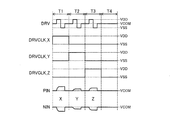
図4に、本実施形態における駆動信号DRV、クロック信号DRVCLK_X,DRVCLK_Y,DRVCLK_Z及び差動信号対PIN,NINの波形の一例を示す。例えば、期間T1〜T4は、それぞれ、クロック信号MCLKのN周期分(例えば1周期分)の期間である。期間T1,T2,T3では、それぞれ、駆動信号DRVの電圧はVCOM(=VDD/2)⇒VDD⇒VSS(=0V)⇒VCOMの順に周期的に変化し、期間T4では、駆動信号DRVの電圧はVCOMである。 FIG. 4 shows an example of waveforms of the drive signal DRV, the clock signals DRVCLK_X, DRVCLK_Y, DRVCLK_Z and the differential signal pair PIN, NIN in the present embodiment. For example, the periods T1 to T4 are N periods (for example, one period) of the clock signal MCLK. In the periods T1, T2 and T3, the voltage of the drive signal DRV cyclically changes in the order of VCOM (=VDD/2) ⇒ VDD ⇒ VSS (=0V) ⇒ VCOM, and in the period T4, the voltage of the drive signal DRV. Is VCOM.
期間T1〜T3では、駆動信号DRVにより物理量検出素子2X,2Y,2Zが共通に駆動され、物理量検出素子2X,2Y,2Zの各々の端子7,8から、X軸、Y軸、Z軸の各方向に加わった物理量に応じた差動信号対が出力される。そして、期間T1では、クロック信号DRVCLK_Xがハイレベルであるため、物理量検出素子2Xから出力される差動対信号が差動信号対PIN,NINとして選択される。また、期間T2では、クロック信号DRVCLK_Yがハイレベルであるため、物理量検出素子2Yから出力される差動対信号が差動信号対PIN,NINとして選択される。また、期間T3では、クロック信号DRVCLK_Zがハイレベルであるため、物理量検出素子2Zから出力される差動対信号が差動信号対PIN,NINとして選択される。また、期間T4では、クロック信号DRVCLK_X,DRVCLK_Y,DRVCLK_Zがいずれもローレベルであるため、差動信号対PIN,NINはいずれもVCOMとなる。
In the periods T1 to T3, the physical
図1に戻り、QVアンプ20は、マルチプレクサー10から出力される電荷の差動信号対PIN,NINを電圧の差動信号対に変換して出力する。容量21,22は、QVアンプ20の帰還容量である。
Returning to FIG. 1, the
プログラマブルゲインアンプ30は、QVアンプ20から出力される差動信号対が容量23,24を介して入力され、当該差動信号を増幅した差動信号対POP,PONを出力する。
The
スイッチトキャパシターフィルター回路50X,50Y,50Zは、プログラマブルゲインアンプ30から出力される差動信号対POP,PONが共通に入力される。そして、スイッチトキャパシターフィルター回路50Xは、クロック信号DRVCLK_Xに基づいて、差動信号対POP,PONに含まれる物理量検出素子2Xの出力信号に基づく信号をサンプリングしてホールドするとともにフィルタリング処理を行い、差動信号対SOP_X,SON_Xを出力する。また、スイッチトキャパシターフィルター回路50Yは、クロック信号DRVCLK_Yに基づいて、差動信号対POP,PONに含まれる物理量検出素子2Yの出力信号に基づく信号をサンプリングしてホールドするとともにフィルタリング処理を行い、差動信号対SOP_Y,SON_Yを出力する。また、スイッチトキャパシターフィルター回路50Zは、クロック信号DRVCLK_Zに基づいて、差動信号対POP,PONに含まれる物理量検出素子2Zの出力信号に基づく信号をサンプリングしてホールドするとともにフィルタリング処理を行い、差動信号対SOP_Z,SON_Zを出力する。本実施形態では、スイッチトキャパシターフィルター回路50X,50Y,50Zは、同じ回路構成で実現される。
The differential signal pair POP and PON output from the
図5は、スイッチトキャパシターフィルター回路50(50X,50Y,50Z)の構成例を示す図である。図5に示すように、スイッチトキャパシターフィルター回路50は、サンプルホールド回路51P,51N、増幅回路52、スイッチトキャパシター回路53P,53N、分周回路54及びクロック生成回路55を含んで構成されている。
FIG. 5 is a diagram showing a configuration example of the switched capacitor filter circuit 50 (50X, 50Y, 50Z). As shown in FIG. 5, the switched
分周回路54は、クロック信号DRVCLK(DRVCLK_X,DRVCLK_Y,DRVCLK_Z)を分周(M分周)してクロック信号CHOPCLK(「第2のクロック信号」の一例)を生成して出力する。また、分周回路54は、クロック信号CHOPCLKのハイレベルとローレベルが反転されたクロック信号nCHOPCLKを生成して出力する。従って、分周回路54の分周比をMとすると、クロック信号CHOPCLK,nCHOPCLKの周波数(チョッピング周波数fc)は、クロック信号DRVCLKの周波数(駆動周波数fd)の1/Mである。
The
クロック生成回路55は、クロック信号DRVCLK(DRVCLK_X,DRVCLK_Y,DRVCLK_Z)に基づいてクロック信号SCFCLKを生成して出力する。本実施形態では、クロック信号SCFCLKは、クロック信号DRVCLKと同じ周波数(駆動周波数fd)であり、クロック信号DRVCLKよりもハイパルスの幅が狭い信号である。
The
サンプルホールド回路51P(「第1のサンプルホールド回路」の一例)は、物理量検出素子2X,2Y,2Zの出力信号に基づく信号であり、プログラマブルゲインアンプ30から出力される信号POP(「第1の信号」の一例)をサンプルホールドする。図5に示すように、サンプルホールド回路51Pは、スイッチS1P,S2P,S3P,S4P及び容量C1Pを含んで構成されている。スイッチS1P,S3Pは、クロック信号SCFCLKがハイレベルのときに導通状態となり、クロック信号SCFCLKがローレベルのときに非導通状態となる。また、スイッチS2P,S4Pは、クロック信号SCFCLKがローレベルのときに導通状態となり、クロック信号SCFCLKがハイレベルのときに非導通状態となる。このサンプルホールド回路51Pは、クロック信号SCFCLKがハイレベルの期間で、プログラマブルゲインアンプ30から出力される信号POPをサンプリングし、クロック信号SCFCLKがローレベルの期間はサンプリングした信号POPをホールドする。
The
サンプルホールド回路51N(「第2のサンプルホールド回路」の一例)は、物理量検出素子2X,2Y,2Zの出力信号に基づく信号であり、プログラマブルゲインアンプ30から出力される信号PON(「第2の信号」の一例)をサンプルホールドする。図5に示すように、サンプルホールド回路51Nは、スイッチS1N,S2N,S3N,S4N及び容量C1Nを含んで構成されている。スイッチS1N,S3Nは、クロック信号SCFCLKがハイレベルのときに導通状態となり、クロック信号SCFCLKがローレベルのときに非導通状態となる。また、スイッチS2N,S4Nは、クロック信号SCFCLKがローレベルのときに導通状態となり、クロック信号SCFCLKがハイレベルのときに非導通状態となる。このサンプルホールド回路51Nは、クロック信号SCFCLKがハイレベルの期間で、プログラマブルゲインアンプ30から出力される信号PONをサンプリングし、クロック信号SCFCLKがローレベルの期間はサンプリングした信号PONをホールドする。
The
増幅回路52は、非反転入力端子(+入力端子)にサンプルホールド回路51Pの出力信号及びスイッチトキャパシター回路53Pの出力信号が入力され、反転入力端子(−入力端子)にサンプルホールド回路51Nの出力信号及びスイッチトキャパシター回路53Nの出力信号が入力される。この増幅回路52は、入力される差動信号対を反転増幅するとともに、クロック信号CHOPCLK,nCHOPCLKに基づくチョッピングを行い、差動信号対SOP,SONを出力する。
In the
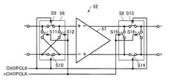
図6は、増幅回路52の構成例を示す図である。図6に示すように、増幅回路52は、チョッピング回路56、演算増幅器57及びチョッピング回路58を含んで構成されている。
FIG. 6 is a diagram showing a configuration example of the
チョッピング回路56(「第1のチョッピング回路」の一例)は、サンプルホールド回路51P,51Nの出力信号(差動信号対)が入力され、クロック信号CHOPCLK,nCHOPCLKに基づいて動作し、当該差動信号対をチョッピングした差動信号対を出力する。図6に示すように、チョッピング回路56は、4つのスイッチS9,S10,S11,S12を含んで構成されている。スイッチS9,S10はクロック信号CHOPCLKがハイレベルのときに導通状態となり、クロック信号CHOPCLKがローレベルのときに非導通状態となる。また、スイッチS11,S12はクロック信号nCHOPCLKがハイレベルのときに導通状態となり、クロック信号nCHOPCLKがローレベルのときに非導通状態となる。ここで、クロック信号nCHOPCLKは、クロック信号CHOPCLKのハイレベルとローレベルが反転された信号であり、クロック信号CHOPCLKがハイレベルのときはクロック信号nCHOPCLKがローレベルとなり、クロック信号CHOPCLKがローレベルのときはクロック信号nCHOPCLKがハイレベルとなる。そして、前述の通り、クロック信号CHOPCLK,nCHOPCLKの周波数(チョッピング周波数)fcは、クロック信号DRVCLKの周波数(駆動周波数fd)の1/Mであるから、クロック信号DRVCLKのM/2周期分の期間(図4に示した期間T1〜T4がM/2回繰り返される期間)毎に、クロック信号CHOPCLKがハイレベルかつクロック信号nCHOPCLKがローレベルとなる状態と、クロック信号CHOPCLKがローレベルかつクロック信号nCHOPCLKがハイレベルとなる状態とが繰り返される。
The chopping circuit 56 (an example of “first chopping circuit”) receives the output signals (differential signal pair) of the
従って、クロック信号DRVCLKのM/2周期分の期間毎に、スイッチS9,S10が導通状態かつスイッチS11,S12が非導通状態となって入力される差動信号対がそのまま出力される状態と、スイッチS9,S10が非導通状態かつスイッチS11,S12が導通状態となって入力される差動信号対が入れ替わって出力される状態とが繰り返される。その結果、チョッピング回路56に入力される差動信号対に含まれるDC付近の信号成分は、チョッピング回路56によってチョッピング周波数fc付近の信号成分に変換される。図7にチョッピング回路56に入力される差動信号対の周波数スペクトラムの一例を示し、図8にチョッピング回路56から出力される差動信号対の周波数スペクトラムの一例を示す。図7及び図8において、横軸は周波数、縦軸はパワーである。また、Sは差動信号対に含まれる信号成分を表し、Nは差動信号対に含まれるノイズ成分を表す。
Therefore, in each period of M/2 cycles of the clock signal DRVCLK, the switches S9 and S10 are in the conductive state and the switches S11 and S12 are in the non-conductive state, and the input differential signal pair is directly output. The state where the switches S9 and S10 are non-conducting and the switches S11 and S12 are conducting and the input differential signal pair is switched and output is repeated. As a result, the signal components near DC included in the differential signal pair input to the
演算増幅器57は、チョッピング回路56の出力信号(差動信号対)が入力され、入力される差動信号対を反転増幅して出力する。この演算増幅器57から出力される差動信号対には、演算増幅器57の動作により発生する1/fノイズが重畳される。図9に演算増幅器57から出力される差動信号対の周波数スペクトラムの一例を示す。図9において、横軸は周波数、縦軸はパワーである。また、Sは差動信号対に含まれる信号成分を表し、Nは差動信号対に含まれるノイズ成分を表す。
The
チョッピング回路58(「第2のチョッピング回路」の一例)は、演算増幅器57の出力信号(差動信号対)が入力され、クロック信号CHOPCLK,nCHOPCLKに基づいて動作し、当該差動信号対をチョッピングした差動信号対を出力する。図6に示すように、チョッピング回路58は、4つのスイッチS13,S14,S15,S16を含んで構成されている。スイッチS13,S14はクロック信号CHOPCLKがハイレベルのときに導通状態となり、クロック信号CHOPCLKがローレベルのときに非導通状態となる。また、スイッチS15,S16はクロック信号nCHOPCLKがハイレベルのときに導通状態となり、クロック信号nCHOPCLKがローレベルのときに非導通状態となる。そして、前述の通り、クロック信号CHOPCLK,nCHOPCLKの周波数(チョッピング周波数)fcは、クロック信号DRVCLKの周波数(駆動周波数fd)の1/Mであるから、クロック信号DRVCLKのM/2周期分の期間(図4に示した期
間T1〜T4がM/2回繰り返される期間)毎に、クロック信号CHOPCLKがハイレベルかつクロック信号nCHOPCLKがローレベルとなる状態と、クロック信号CHOPCLKがローレベルかつクロック信号nCHOPCLKがハイレベルとなる状態とが繰り返される。
The chopping circuit 58 (an example of “second chopping circuit”) receives the output signal (differential signal pair) of the
従って、クロック信号DRVCLKのM/2周期分の期間毎に、スイッチS13,S14が導通状態かつスイッチS15,S16が非導通状態となって入力される差動信号対がそのまま出力される状態と、スイッチS13,S14が非導通状態かつスイッチS15,S16が導通状態となって入力される差動信号対が入れ替わって出力される状態とが繰り返される。その結果、チョッピング回路58に入力される差動信号対に含まれるチョッピング周波数fc付近の信号成分は、チョッピング回路58によってDC付近の信号成分に戻され、当該差動信号対に含まれるノイズ成分(1/fノイズ)はチョッピング周波数fc付近のノイズ成分に変換される。図10にチョッピング回路58から出力される差動信号対の周波数スペクトラムの一例を示す。図10において、横軸は周波数、縦軸はパワーである。また、Sは差動信号対に含まれる信号成分を表し、Nは差動信号対に含まれるノイズ成分を表す。
Therefore, for each period of M/2 cycles of the clock signal DRVCLK, the switches S13 and S14 are in the conductive state and the switches S15 and S16 are in the non-conductive state, and the input differential signal pair is output as it is, The state where the switches S13 and S14 are non-conducting and the switches S15 and S16 are conducting and the input differential signal pair is switched and output is repeated. As a result, the signal component near the chopping frequency fc included in the differential signal pair input to the
そして、チョッピング回路58から出力される差動信号対は、増幅回路52の出力信号(差動信号対SOP,SON)となる。このように、演算増幅器57の前段と後段に設けられたチョッピング回路56,58により、演算増幅器57の動作により発生し、差動信号対SOP,SONにおいてDC付近の信号帯域に含まれるノイズを効果的に低減させることができる。
The differential signal pair output from the chopping
図5に戻り、スイッチトキャパシター回路53P(「第1のスイッチトキャパシター回路」の一例)は、増幅回路52の反転出力端子(−出力端子)から出力される出力信号SOP(「増幅回路の第1の出力信号」の一例)が入力される。図5に示すように、スイッチトキャパシター回路53Pは、スイッチS5P,S6P,S7P,S8P及び容量C2P,C3Pを含んで構成されている。スイッチS5P,S8Pは、クロック信号SCFCLKがローレベルのときに導通状態となり、クロック信号SCFCLKがハイレベルのときに非導通状態となる。また、スイッチS6P,S7Pは、クロック信号SCFCLKがハイレベルのときに導通状態となり、クロック信号SCFCLKがローレベルのときに非導通状態となる。このスイッチトキャパシター回路53Pは、クロック信号SCFCLKの周波数及び容量C2P,C3Pの容量値によって決まるカットオフ周波数を有するロー
パスフィルターとして機能する。
Returning to FIG. 5, the switched
スイッチトキャパシター回路53N(「第2のスイッチトキャパシター回路」の一例)は、増幅回路52の非反転出力端子(+出力端子)から出力される出力信号SON(「増幅回路の第2の出力信号」の一例)が入力される。図5に示すように、スイッチトキャパシター回路53Nは、スイッチS5N,S6N,S7N,S8N及び容量C2N,C3Nを含んで構成されている。スイッチS5N,S8Nは、クロック信号SCFCLKがローレベルのときに導通状態となり、クロック信号SCFCLKがハイレベルのときに非導通状態となる。また、スイッチS6N,S7Nは、クロック信号SCFCLKがハイレベルのときに導通状態となり、クロック信号SCFCLKがローレベルのときに非導通状態となる。このスイッチトキャパシター回路53Nは、クロック信号SCFCLKの周波数及び容量C2N,C3Nの容量値によって決まるカットオフ周波数を有するローパスフィルターとして機能する。
The switched
このように構成されているスイッチトキャパシターフィルター回路50は、クロック信号SCFCLKに基づき、プログラマブルゲインアンプ30から出力される信号(差動信号対POP,PON)に対して差動で動作し、差動信号対SOP,SONを出力する。そして、クロック信号SCFCLKの周波数は、クロック信号DRVCLKと同じ周波数(駆動周波数fd)であるので、プログラマブルゲインアンプ30から出力される差動信号対POP,PONの更新レートと同じである。従って、サンプルホールド回路51P,51Nにおける、クロック信号SCFCLKによる差動信号対POP,PONのサンプリングは、サンプリング定理を満たしていない。そこで、本実施形態では、差動信号対POP,PONがピーク値を維持している期間にクロック信号SCFCLKの立ち下がりのタイミングが到来するように、クロック信号SCFCLKの位相が調整されている(図11参照)。これにより、クロック信号SCFCLKの1周期毎に差動信号対POP,PONのピーク値が変化するような場合、すなわち、物理量検出素子2に加わる物理量(加速度)の変化が極めて速い場合は、スイッチトキャパシターフィルター回路50によるフィルター処理が正しく機能しないが、通常は、クロック信号SCFCLKの周期と比較して物理量(加速度)の変化の周期は十分長いので、フィルター処理が正しく機能する。そして、クロック信号SCFCLKの周期と比較して物理量(加速度)の変化の周期が十分遅い場合、差動信号対POP,PONのピーク値の変化の周期も長いので、サンプルホールド回路51P,51Nの出力信号はDCに近い信号となる。そのため、スイッチトキャパシターフィルター回路50が出力する差動信号対SOP,SONもDCに近い信号となる。
The switched
図1に戻り、温度センサー40は、温度に応じて電圧が変化する信号TOを出力する。温度センサー40は、例えば、基準温度(例えば、+25℃)における信号TOの電圧が基準電圧VCOMとなるように調整されている。温度センサー40は、例えば、バンドギャップリファレンス回路の温度特性を利用した回路であってもよい。
Returning to FIG. 1, the
マルチプレクサー60は、互いに排他的にアクティブ(本実施形態では、ハイレベル)
となる制御信号EN_OUT_X,EN_OUT_Y,EN_OUT_Z,EN_OUT_Tに基づいて、スイッチトキャパシターフィルター回路50Xが出力する差動信号対SOP_X,SON_X、スイッチトキャパシターフィルター回路50Yが出力する差動信号対SOP_Y,SON_Y、スイッチトキャパシターフィルター回路50Zが出力する差動信号対SOP_Z,SON_Z、温度センサー40の出力信号TOのいずれかを選択して(又はいずれも選択しないで)信号対MOP,MONを出力する。具体的には、マルチプレクサー60は、制御信号EN_OUT_Xがハイレベルのときは、差動信号対SOP_X,SON_Xを選択し、差動信号対MOP,MONとして出力する。また、マルチプレクサー60は、制御信号EN_OUT_Yがハイレベルのときは、差動信号対SOP_Y,SON_Yを選択し、差動信号対MOP,MONとして出力する。また、マルチプレクサー60は、制御信号EN_OUT_Zがハイレベルのときは、差動信号対SOP_Z,SON_Zを選択し、差動信号対MOP,MONとして出力する。また、マルチプレクサー60は、制御信号EN_OUT_Tがハイレベルのときは、温度センサー40の出力信号TOを選択し、信号TOと基準電圧VCOMとの信号対を信号対MOP,MONとして出力する。
The
Based on the control signals EN_OUT_X, EN_OUT_Y, EN_OUT_Z, EN_OUT_T, the differential signal pair SOP_X, SON_X output by the switched
A/D変換回路70は、クロック信号SMPCLKに基づいて、マルチプレクサー60が出力する信号対MOP,MON(差動信号対SOP_X,SON_X、差動信号対SOP_Y,SON_Y、差動信号対SOP_Z,SON_Z又は信号対TO,VCOM)をサンプリングし、信号対MOP,MONの電位差をデジタル信号に変換する。クロック信号SMPCLKは、制御信号EN_OUT_X,EN_OUT_Y,EN_OUT_Z,EN_OUT_Tがそれぞれハイレベルの期間に1つずつハイパルスを含むクロック信号である。そして、A/D変換回路70は、制御信号EN_OUT_Xがハイレベルの期間のクロック信号SMPCLKの立ち上がりで、マルチプレクサー60から出力される信号対MOP,MON(スイッチトキャパシターフィルター回路50Xが出力する差動信号対SOP_X,SON_X)をサンプリングしてデジタル信号に変換する。また、A/D変換回路70は、制御信号EN_OUT_Yがハイレベルの期間のクロック信号SMPCL
Kの立ち上がりで、マルチプレクサー60から出力される信号対MOP,MON(スイッチトキャパシターフィルター回路50Yが出力する差動信号対SOP_Y,SON_Y)をサンプリングしてデジタル信号に変換する。また、A/D変換回路70は、制御信号EN_OUT_Zがハイレベルの期間のクロック信号SMPCLKの立ち上がりで、マルチプレクサー60から出力される信号対MOP,MON(スイッチトキャパシターフィルター回路50Zが出力する差動信号対SOP_Z,SON_Z)をサンプリングしてデジタル信号に変換する。また、A/D変換回路70は、制御信号EN_OUT_Tがハイレベルの期間のクロック信号SMPCLKの立ち上がりで、マルチプレクサー60から出力される信号対MOP,MON(温度センサー40の出力信号TOと基準電圧VCOMとの信号対)をサンプリングしてデジタル信号に変換する。
Based on the clock signal SMPCLK, the A/
At the rising edge of K, the signal pair MOP, MON output from the multiplexer 60 (differential signal pair SOP_Y, SON_Y output by the switched
このように、A/D変換回路70は、期間T1〜T4において、マルチプレクサー60から出力される信号対MOP,MONを複数回(ここでは4回)サンプリングして時分割にA/D変換する。すなわち、A/D変換回路70は、スイッチトキャパシターフィルター回路50X,50Y,50Zの出力信号(差動信号対)を含む複数の信号を時分割にA/D変換する。前述の通り、本実施形態では、スイッチトキャパシターフィルター回路50X,50Y,50Zがそれぞれ出力する差動信号対はいずれもDCに近い信号であり、また、温度センサー40の出力信号TOもDCに近い信号であるから、マルチプレクサー60における信号の選択タイミングの制約が少ない。換言すれば、A/D変換回路70のサンプリングタイミングの自由度が高い。
In this way, the A/
なお、サンプリング定理に基づき、スイッチトキャパシターフィルター回路50X,50Y,50Zの出力信号において、サンプリング周波数fs(A/D変換回路70がスイッチトキャパシターフィルター回路50X,50Y,50Zの出力信号をそれぞれサンプリングする周波数)の1/2よりも高い信号成分は、A/D変換回路70におけるサンプリングにより、DC近傍の周波数帯に折り返されてノイズ成分となる。そのため、スイッチトキャパシターフィルター回路50X,50Y,50Zは、DCに近い信号を発生させるサンプルホールド回路として機能するとともに、A/D変換回路70のサンプリングにより生ずるノイズ成分を低減させるためのアンチエイリアスフィルターとしても機能するように、そのカットオフ周波数はサンプリング周波数fsの1/2以下に設定される。
Based on the sampling theorem, the sampling frequency fs (the frequency at which the A/
また、スイッチトキャパシターフィルター回路50X,50Y,50Zから出力される差動信号対SOP_X,SON_X、差動信号対SOP_Y,SON_Y及び差動信号対SOP_Z,SON_Zは、チョッピング周波数fc付近のノイズ成分が高いため(図10参照)、A/D変換回路70のサンプリングによってこのノイズ成分がDC付近の信号帯域に折り返さないように、チョッピング周波数fcは、サンプリング周波数fsの1/2以下に設定される。
Further, the differential signal pair SOP_X, SON_X, the differential signal pair SOP_Y, SON_Y and the differential signal pair SOP_Z, SON_Z output from the switched
デジタルフィルター80は、クロック信号MCLKに基づいて、A/D変換回路70から出力されるデジタル信号に対してフィルタリング処理を行う。A/D変換回路70から出力されるデジタル信号には、A/D変換回路70のA/D変換処理により発生した高周波ノイズが重畳されているため、デジタルフィルター80は、この高周波ノイズを低減させるローパスフィルターとして機能する。
The
また、デジタルフィルター80は、さらに、温度センサーの出力信号TOが変換されたデジタル信号を用いて、スイッチトキャパシターフィルター回路50X,50Y,50Zからそれぞれ出力される差動信号対の温度特性を補正する処理を行ってもよい。
Further, the
インターフェース回路120は、物理量検出装置1の外部装置と通信するための回路である。外部装置は、インターフェース回路120を介して、記憶部130に対するデータ
の書き込みや読み出し、デジタルフィルター80から出力されるデジタル信号の読み出し等を行うことができる。インターフェース回路120は、例えば、3端子や4端子のSPI(Serial Peripheral Interface)インターフェース回路であってもよいし、2端子のI2C(Inter-Integrated Circuit)インターフェース回路であってもよい。
The
記憶部130は、レジスター131及び不揮発性メモリー132を有している。不揮発性メモリー132には、物理量検出回路3に含まれる各回路に対する各種のデータ(例えば、プログラマブルゲインアンプ30の利得調整データ、温度センサー40の出力調整データ、デジタルフィルター80のフィルター係数や温度補正テーブル)等の各種の情報が記憶されている。不揮発性メモリー132は、例えば、MONOS(Metal Oxide Nitride Oxide Silicon)型メモリーやEEPROM(Electrically Erasable Programmable Read-Only Memory)として構成することができる。また、物理量検出回路3の電源投入時(電源電圧が0VからVDDまで立ち上がる時)に、不揮発性メモリー132に記憶されている各種のデータがレジスター131に転送されて保持され、レジスター131に保持された各種のデータが各回路に供給される。
The
以上に説明した物理量検出回路3における各種信号の信号波形の一例を図11及び図12に示す。図11及び図12に示すように、クロック信号SCFCLK(SCFCLK_X,SCFCLK_Y,SCFCLK_Z)の周波数は、クロック信号DRVCLK(DRVCLK_X,DRVCLK_Y,DRVCLK_Z)と同じ周波数(駆動周波数fd)である。また、サンプリング周波数fsは駆動周波数fdの1/4であり、チョッピング周波数fcは駆動周波数fdの1/16である。 11 and 12 show examples of signal waveforms of various signals in the physical quantity detection circuit 3 described above. As shown in FIGS. 11 and 12, the frequency of the clock signal SCFCLK (SCFCLK_X, SCFCLK_Y, SCFCLK_Z) is the same frequency (driving frequency fd) as the clock signal DRVCLK (DRVCLK_X, DRVCLK_Y, DRVCLK_Z). The sampling frequency fs is 1/4 of the driving frequency fd, and the chopping frequency fc is 1/16 of the driving frequency fd.
なお、物理量検出装置1による物理量の検出精度を向上させるためには、サンプリング周波数fsは駆動周波数fd以下で、A/D変換回路70が動作可能なできるだけ高い周波数であることが望ましい。また、物理量検出装置1による物理量の検出信号(デジタルフィルター80の出力信号)のS/Nを向上させるためには、チョッピング周波数fcは、サンプリング周波数fsの1/2以下で、できるだけ高い周波数であることが望ましい。実際には、サンプリング周波数fsやチョッピング周波数fcは、回路の動作速度の限界や消費電力とのトレードオフを考慮して最適な周波数に決定される。
In order to improve the detection accuracy of the physical quantity by the physical
以上に説明したように、本実施形態の物理量検出装置1(物理量検出回路3)では、スイッチトキャパシターフィルター回路50X,50Y,50Zは、それぞれ、スイッチトキャパシター回路53P,53NによってA/D変換回路70の前段のアンチエイリアスフィルターとして機能する。また、サンプルホールド回路51P,51Nによってスイッチトキャパシターフィルター回路50X,50Y,50Zの出力信号はDCに近い信号となるため、A/D変換回路70によるサンプリングタイミングの自由度が高い。さらに、スイッチトキャパシターフィルター回路50X,50Y,50Zは、入力される差動信号対POP,PONに対して差動で動作するので、差動信号対POP,PONに含まれる同相ノイズや差動信号対POP,PONに対する信号処理で発生する同相ノイズが低減される。従って、本実施形態の物理量検出装置1(物理量検出回路3)によれば、A/D変換回路70のサンプリング周波数fsを変えずに駆動周波数fdを高めることが可能であり、低ノイズ化が可能である。
As described above, in the physical quantity detection device 1 (physical quantity detection circuit 3) of the present embodiment, the switched
また、本実施形態の物理量検出装置1(物理量検出回路3)では、スイッチトキャパシターフィルター回路50X,50Y,50Zにおいて、それぞれ、サンプルホールド回路51P,51Nの出力信号に含まれるDC付近の信号成分は、チョッピング回路56によってチョッピング周波数fc付近の信号成分に変換される。また、演算増幅器57の出力信号に含まれるチョッピング周波数fc付近の信号成分(チョッピング回路56によって変換された信号成分)は、チョッピング回路58によってDC付近の信号成分に戻され、
演算増幅器57の出力信号に含まれるノイズ成分(演算増幅器57の動作により発生する1/fノイズ)は、チョッピング回路58によってチョッピング周波数fc付近のノイズ成分に変換される。従って、本実施形態の物理量検出装置1(物理量検出回路3)によれば、スイッチトキャパシターフィルター回路50X,50Y,50Zの出力信号に含まれるノイズ成分が低減され、さらなる低ノイズ化が可能である。
Further, in the physical quantity detection device 1 (physical quantity detection circuit 3) of the present embodiment, in the switched
The noise component included in the output signal of the operational amplifier 57 (1/f noise generated by the operation of the operational amplifier 57) is converted into a noise component near the chopping frequency fc by the chopping
さらに、本実施形態の物理量検出装置1(物理量検出回路3)では、スイッチトキャパシターフィルター回路50X,50Y,50Zの出力信号はDCに近い信号となるため、A/D変換回路70によるサンプリングタイミングの自由度が高いので、A/D変換回路70において、スイッチトキャパシターフィルター回路50X,50Y,50Zの出力信号及び温度センサー40の出力信号のA/D変換処理を時分割に行うことが可能である。従って、本実施形態によれば、回路面積の大幅な増加を抑制しながら、3軸の物理量検出信号及び温度信号を出力可能な物理量検出装置1(物理量検出回路3)を実現することができる。
Further, in the physical quantity detection device 1 (physical quantity detection circuit 3) of the present embodiment, the output signals of the switched
2.電子機器
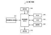
図13は、本実施形態の電子機器の構成の一例を示す機能ブロック図である。図13に示すように、本実施形態の電子機器300は、物理量検出装置310、制御装置(MCU)320、操作部330、ROM(Read Only Memory)340、RAM(Random Access Memory)350、通信部360、表示部370を含んで構成されている。なお、本実施形態の電子機器は、図13の構成要素(各部)の一部を省略又は変更し、あるいは、他の構成要素を付加した構成としてもよい。
2. Electronic Device FIG. 13 is a functional block diagram showing an example of the configuration of the electronic device of this embodiment. As shown in FIG. 13, the electronic device 300 of this embodiment includes a physical
物理量検出装置310は、不図示の物理量検出素子を駆動し、当該物理量検出素子の出力信号に基づいて物理量信号を生成して出力する装置であり、例えば、加速度、角速度、速度、角加速度、力等の物理量の少なくとも一部を検出する慣性計測装置であってもよいし、傾斜角を計測する傾斜計であってもよい。物理量検出装置310として、例えば、上述した本実施形態の物理量検出装置1を適用することができる。
The physical
制御装置(MCU)320は、ROM340等に記憶されているプログラムに従い、物理量検出装置310に通信信号を発信し、物理量検出装置310の出力データを用いて各種の計算処理や制御処理を行う。その他、制御装置(MCU)320は、操作部330からの操作信号に応じた各種の処理、外部装置とデータ通信を行うために通信部360を制御する処理、表示部370に各種の情報を表示させるための表示信号を送信する処理等を行う。
The control unit (MCU) 320 transmits a communication signal to the physical
操作部330は、操作キーやボタンスイッチ等により構成される入力装置であり、ユーザーによる操作に応じた操作信号を制御装置(MCU)320に出力する。
The
ROM340は、制御装置(MCU)320が各種の計算処理や制御処理を行うためのプログラムやデータ等を記憶している。
The
RAM350は、制御装置(MCU)320の作業領域として用いられ、ROM340から読み出されたプログラムやデータ、操作部330から入力されたデータ、制御装置(MCU)320が各種プログラムに従って実行した演算結果等を一時的に記憶する。
The
通信部360は、制御装置(MCU)320と外部装置との間のデータ通信を成立させるための各種制御を行う。
The
表示部370は、LCD(Liquid Crystal Display)等により構成される表示装置であり、制御装置(MCU)320から入力される表示信号に基づいて各種の情報を表示する。表示部370には操作部330として機能するタッチパネルが設けられていてもよい。
The
物理量検出装置310として、例えば上述した本実施形態の物理量検出装置1を適用することにより、低ノイズ化が可能であるので、信頼性の高い電子機器を実現することができる。
By applying, for example, the above-described physical
このような電子機器300としては種々の電子機器が考えられ、例えば、パーソナルコンピューター(例えば、モバイル型パーソナルコンピューター、ラップトップ型パーソナルコンピューター、タブレット型パーソナルコンピューター)、スマートフォンや携帯電話機などの移動体端末、デジタルカメラ、インクジェット式吐出装置(例えば、インクジェットプリンター)、ルーターやスイッチなどのストレージエリアネットワーク機器、ローカルエリアネットワーク機器、移動体端末基地局用機器、テレビ、ビデオカメラ、ビデオレコーダー、カーナビゲーション装置、リアルタイムクロック装置、ページャー、電子手帳(通信機能付も含む)、電子辞書、電卓、電子ゲーム機器、ゲーム用コントローラー、ワードプロセッサー、ワークステーション、テレビ電話、防犯用テレビモニター、電子双眼鏡、POS端末、医療機器(例えば電子体温計、血圧計、血糖計、心電図計測装置、超音波診断装置、電子内視鏡)、魚群探知機、各種測定機器、計器類(例えば、車両、航空機、船舶の計器類)、フライトシミュレーター、ヘッドマウントディスプレイ、モーショントレース、モーショントラッキング、モーションコントローラー、PDR(歩行者位置方位計測)等が挙げられる。 Various electronic devices can be considered as the electronic device 300. For example, a personal computer (for example, a mobile personal computer, a laptop personal computer, a tablet personal computer), a mobile terminal such as a smartphone or a mobile phone, Digital cameras, inkjet discharge devices (eg inkjet printers), storage area network devices such as routers and switches, local area network devices, mobile terminal base station devices, televisions, video cameras, video recorders, car navigation devices, real time Clock devices, pagers, electronic notebooks (including communication functions), electronic dictionaries, calculators, electronic game devices, game controllers, word processors, workstations, videophones, crime prevention TV monitors, electronic binoculars, POS terminals, medical devices ( For example, electronic thermometer, sphygmomanometer, blood glucose meter, electrocardiogram measuring device, ultrasonic diagnostic device, electronic endoscope), fish finder, various measuring instruments, measuring instruments (for example, measuring instruments for vehicles, aircrafts, ships), flight simulators , Head mounted display, motion trace, motion tracking, motion controller, PDR (pedestrian position and orientation measurement), and the like.
図14は、本実施形態の電子機器300の一例であるデジタルカメラ1300を模式的に示す斜視図である。なお、図14には、外部機器との接続についても簡易的に示している。ここで、通常のカメラは、被写体の光像により銀塩写真フィルムを感光するのに対し、デジタルカメラ1300は、被写体の光像をCCD(Charge Coupled Device)などの撮像素子により光電変換して撮像信号(画像信号)を生成する。
FIG. 14 is a perspective view schematically showing a
デジタルカメラ1300におけるケース(ボディー)1302の背面には、表示部1310が設けられ、CCDによる撮像信号に基づいて表示を行う構成になっており、表示部1310は、被写体を電子画像として表示するファインダーとして機能する。また、ケース1302の正面側(図中裏面側)には、光学レンズ(撮像光学系)やCCDなどを含む受光ユニット1304が設けられている。撮影者が表示部1310に表示された被写体像を確認し、シャッターボタン1306を押下すると、その時点におけるCCDの撮像信号が、メモリー1308に転送・格納される。また、このデジタルカメラ1300においては、ケース1302の側面に、ビデオ信号出力端子1312と、データ通信用の入出力端子1314とが設けられている。そして、ビデオ信号出力端子1312には、テレビモニター1430が、データ通信用の入出力端子1314には、パーソナルコンピューター1440が、それぞれ必要に応じて接続される。さらに、所定の操作により、メモリー1308に格納された撮像信号が、テレビモニター1430や、パーソナルコンピューター1440に出力される構成になっている。デジタルカメラ1300は、物理量検出装置310を有し、物理量検出装置310の出力データを用いて、例えば手振れ補正等の処理を行う。
A
3.移動体
図15は、本実施形態の移動体の一例を示す図(上面図)である。図15に示す移動体400は、物理量検出装置410,420,430、コントローラー440,450,460、バッテリー470、ナビゲーション装置480を含んで構成されている。なお、本実施形態の移動体は、図15の構成要素(各部)の一部を省略し、あるいは、他の構成要素を付加した構成としてもよい。
3. Moving Body FIG. 15 is a diagram (top view) showing an example of the moving body of the present embodiment. The moving
物理量検出装置410,420,430、コントローラー440,450,460、ナビゲーション装置480は、バッテリー470から供給される電源電圧で動作する。
The physical
コントローラー440,450,460は、それぞれ、物理量検出装置410,420,430に通信信号を発信し、物理量検出装置410,420,430の各出力データを用いて、姿勢制御システム、横転防止システム、ブレーキシステム等の各種の制御を行う制御装置である。
The
ナビゲーション装置480は、内蔵のGPS受信機(不図示)の出力情報に基づき、移動体400の位置や時刻その他の各種の情報をディスプレイに表示する。また、ナビゲーション装置480は、物理量検出装置490を内蔵しており、GPSの電波が届かない時でも物理量検出装置490の出力信号に基づいて移動体400の位置や向きの計算を行い、必要な情報の表示を継続する。
The
物理量検出装置410,420,430,490は、不図示の物理量検出素子を駆動し、当該物理量検出素子の出力信号に基づいて物理量信号を生成して出力する装置であり、それぞれ、例えば、加速度センサー、角速度センサー、速度センサー、傾斜計等である。
The physical
例えば、物理量検出装置410,420,430,490として、上述した各実施形態の物理量検出装置1を適用することにより、低ノイズ化が可能であるので、信頼性の高い移動体を実現することができる。
For example, by applying the physical
このような移動体400としては種々の移動体が考えられ、例えば、自動車(電気自動車も含む)、ジェット機やヘリコプター等の航空機、船舶、ロケット、人工衛星等が挙げられる。
Various types of moving bodies are conceivable as such moving
本発明は本実施形態に限定されず、本発明の要旨の範囲内で種々の変形実施が可能である。 The present invention is not limited to this embodiment, and various modifications can be made within the scope of the gist of the present invention.
例えば、上述した実施形態では、加速度を検出する物理量検出素子を含む物理量検出装置(加速度検出装置)、電子機器及び移動体を例に挙げて説明したが、本発明は、種々の物理量を検出する物理量検出素子を含む物理量検出装置、電子機器及び移動体にも適用することができる。物理量検出素子が検出する物理量は、加速度に限らず、角速度、角加速度、地磁気、傾斜などであってもよい。また、物理量検出素子の振動片の材料としては、Si(シリコン)等の半導体材料の代わりに、例えば、水晶(SiO2)、タンタル酸リチウム(LiTaO3)、ニオブ酸リチウム(LiNbO3)等の圧電単結晶やジルコン酸チタン酸鉛(PZT)等の圧電セラミックスなどの圧電性材料を用いてもよいし、シリコン半導体を用いてもよい。また、例えば、シリコン半導体の表面の一部に、駆動電極に挟まれた酸化亜鉛(ZnO)、窒化アルミニウム(AlN)等の圧電薄膜を配置した構造であってもよい。また、物理量検出素子は、静電容量型の素子に限らず、圧電型、動電型、渦電流型、光学型、ひずみゲージ型等の振動式の素子であってもよい。あるいは、物理量検出素子の方式は、振動式に限らず、例えば、光学式、回転式、流体式であってもよい。 For example, in the above-described embodiment, the physical quantity detection device (acceleration detection device) including the physical quantity detection element that detects acceleration, the electronic device, and the moving body have been described as examples, but the present invention detects various physical quantities. It can also be applied to a physical quantity detection device including a physical quantity detection element, an electronic device, and a moving body. The physical quantity detected by the physical quantity detection element is not limited to acceleration, but may be angular velocity, angular acceleration, geomagnetism, inclination, or the like. Further, as the material of the resonator element of the physical quantity detection element, instead of a semiconductor material such as Si (silicon), for example, quartz (SiO 2 ), lithium tantalate (LiTaO 3 ), lithium niobate (LiNbO 3 ) or the like is used. A piezoelectric material such as a piezoelectric single crystal or piezoelectric ceramics such as lead zirconate titanate (PZT) may be used, or a silicon semiconductor may be used. Further, for example, a structure in which a piezoelectric thin film such as zinc oxide (ZnO) or aluminum nitride (AlN) sandwiched between drive electrodes may be arranged on a part of the surface of a silicon semiconductor. Further, the physical quantity detection element is not limited to the capacitance type element, and may be a vibration type element such as a piezoelectric type, an electrodynamic type, an eddy current type, an optical type, or a strain gauge type. Alternatively, the method of the physical quantity detection element is not limited to the vibration type, and may be, for example, an optical type, a rotary type, or a fluid type.
また、例えば、上述した各実施形態では、A/D変換回路70は、3軸の加速度信号及び温度信号を時分割にA/D変換処理を行っているが、これらの一部を他の物理量信号(角速度信号等)に置き換えて時分割にA/D変換処理を行ってもよいし、他の物理量信号を追加して時分割にA/D変換処理を行ってもよい。
Further, for example, in each of the above-described embodiments, the A/
また、例えば、上述した各実施形態では、スイッチトキャパシターフィルター回路50
X,50Y,50Zは、入力される差動信号対POP,PONに対して差動で動作しているが、シングルエンド信号が入力され、差動で動作しなくてもよい。
Further, for example, in each of the above-described embodiments, the switched
Although X, 50Y, and 50Z operate differentially with respect to the input differential signal pair POP and PON, they do not have to operate differentially because a single-end signal is input.
上述した実施形態および変形例は一例であって、これらに限定されるわけではない。例えば、各実施形態および各変形例を適宜組み合わせることも可能である。 The above-described embodiments and modifications are examples, and the present invention is not limited to these. For example, each embodiment and each modification can be combined as appropriate.
本発明は、実施の形態で説明した構成と実質的に同一の構成(例えば、機能、方法及び結果が同一の構成、あるいは目的及び効果が同一の構成)を含む。また、本発明は、実施の形態で説明した構成の本質的でない部分を置き換えた構成を含む。また、本発明は、実施の形態で説明した構成と同一の作用効果を奏する構成又は同一の目的を達成することができる構成を含む。また、本発明は、実施の形態で説明した構成に公知技術を付加した構成を含む。 The present invention includes configurations substantially the same as the configurations described in the embodiments (for example, configurations having the same function, method and result, or configurations having the same object and effect). Further, the invention includes configurations in which non-essential parts of the configurations described in the embodiments are replaced. Further, the invention includes a configuration that achieves the same effect as the configuration described in the embodiment or a configuration that can achieve the same object. Further, the invention includes configurations in which known techniques are added to the configurations described in the embodiments.
1…物理量検出装置、2,2X,2Y,2Z…物理量検出素子、3…物理量検出回路、5…第1容量形成部、6…第2容量形成部,7,8,9…端子、10…マルチプレクサー、20…Q/Vアンプ、21〜24…容量、30…プログラマブルゲインアンプ、31,32…容量、40…温度センサー、50,50X,50Y,50Z…スイッチトキャパシターフィルター回路、51P,51N…サンプルホールド回路、52…増幅回路、53P,53N…スイッチトキャパシター回路、54…分周回路、55…クロック生成回路、56…チョッピング回路、57…演算増幅器、58…チョッピング回路、60…マルチプレクサー、70…A/D変換回路、80…デジタルフィルター、90…発振回路、100…制御回路、110…駆動回路、120…インターフェース回路、130…記憶部、131…レジスター、132…不揮発性メモリー、200…固定部、201〜204…固定電極、210…可動部、211…錘部、211A,211B…可動電極、212…ばね部、300…電子機器、310…物理量検出装置、320…制御装置(MCU)、330…操作部、340…ROM、350…RAM、360…通信部、370…表示部、400…移動体、410,420,430…物理量検出装置、440,450,460…コントローラー、470…バッテリー、480…ナビゲーション装置、490…物理量検出装置、1300…デジタルカメラ、1302…ケース、1304…受光ユニット、1306…シャッターボタン、1308…メモリー、1310…表示部、1312…ビデオ信号出力端子、1314…入出力端子、1430…テレビモニター、1440…パーソナルコンピューター、C1N,C2N,C3N…容量、C1P,C2P,C3P…容量、S9,S10,S11,S12,S13,S14…スイッチ、S1N,S2N,S3N,S4N,S5N,S6N,S7N,S8N…スイッチ、S1P,S2P,S3P,S4P,S5P,S6P,S7P,S8P…スイッチ
DESCRIPTION OF
Claims (8)
前記スイッチトキャパシターフィルター回路の出力信号をA/D変換するA/D変換回路と、を含み、
前記増幅回路は、
前記第1のサンプルホールド回路の出力信号が入力される第1のチョッピング回路と、
前記第1のチョッピング回路の出力信号が入力される演算増幅器と、
前記演算増幅器の出力信号が入力される第2のチョッピング回路と、
を含む、物理量検出回路。 The first sample-and-hold circuit, an amplifier circuit output signal is input to the first sample-and-hold circuit, and a first output signal of the amplifier circuit for sampling and holding the first signal based on the output signal of the physical quantity detection device A switched capacitor filter circuit including a first switched capacitor circuit to which is input, and an output signal of the first switched capacitor circuit is input to the amplifier circuit;
An A / D converting circuit for the output signal A / D conversion of the switched capacitor filter circuit, only including,
The amplifier circuit is
A first chopping circuit to which the output signal of the first sample and hold circuit is input;
An operational amplifier to which the output signal of the first chopping circuit is input;
A second chopping circuit to which the output signal of the operational amplifier is input;
A physical quantity detection circuit including .
前記第1のチョッピング回路及び前記第2のチョッピング回路におけるチョッピング周波数は、前記A/D変換回路が前記スイッチトキャパシターフィルター回路の出力信号をサンプリングするサンプリング周波数の1/2以下である、物理量検出回路。 In claim 1,
Chopping frequency in the first chopping circuit and the second chopping circuit, the A / D conversion circuit is less half the sampling frequency for sampling the output signal of the switched capacitor filter circuit, physical quantity detection circuit.
第1のクロック信号に基づいて、前記物理量検出素子を駆動する駆動信号を生成する駆動回路を含み、
前記スイッチトキャパシターフィルター回路は、
前記第1のクロック信号を分周して第2のクロック信号を生成する分周回路を含み、
前記第1のチョッピング回路及び前記第2のチョッピング回路は、前記第2のクロック信号に基づいて動作する、物理量検出回路。 In claim 1 or 2,
A drive circuit for generating a drive signal for driving the physical quantity detection element based on a first clock signal;
The switched capacitor filter circuit is
A divider circuit for dividing the first clock signal to generate a second clock signal,
The first chopping circuit and the second chopping circuit operates on the basis of the second clock signal, the physical quantity detection circuit.
前記A/D変換回路は、
前記スイッチトキャパシターフィルター回路の出力信号を含む複数の信号を時分割にA/D変換する、物理量検出回路。 In any one of Claim 1 thru|or 3,
The A/D conversion circuit is
A / D conversion in time division a plurality of signals including the output signal of the switched capacitor filter circuit, physical quantity detection circuit.
前記スイッチトキャパシターフィルター回路は、
前記物理量検出素子の出力信号に基づく第2の信号をサンプルホールドする第2のサンプルホールド回路と、
前記増幅回路の第2の出力信号が入力される第2のスイッチトキャパシター回路と、
を含み、
前記増幅回路は、
前記第1のサンプルホールド回路の出力信号と前記第2のサンプルホールド回路の出力信号とが入力され、
前記第1の信号及び前記第2の信号に対して差動で動作する、物理量検出回路。 In any one of Claim 1 thru|or 4,
The switched capacitor filter circuit is
A second sample and hold circuit for sampling and holding a second signal based on the output signal of the physical quantity detection element;
A second switched capacitor circuit to which the second output signal of the amplifier circuit is input;
Including
The amplifier circuit is
The output signal of the first sample and hold circuit and the output signal of the second sample and hold circuit are input,
Operating at differential with respect to the first signal and the second signal, physical quantity detection circuit.
前記物理量検出素子と、
を備えている、物理量検出装置。 A physical quantity detection circuit according to any one of claims 1 to 5 ,
The physical quantity detection element,
A physical quantity detection device comprising:
Priority Applications (3)
| Application Number | Priority Date | Filing Date | Title |
|---|---|---|---|
| JP2016140347A JP6733381B2 (en) | 2016-07-15 | 2016-07-15 | Physical quantity detection circuit, physical quantity detection device, electronic device and moving body |
| CN201710521602.5A CN107632169A (en) | 2016-07-15 | 2017-06-30 | Physical quantity detection circuit, measuring physical, electronic equipment and moving body |
| US15/646,376 US10116275B2 (en) | 2016-07-15 | 2017-07-11 | Physical quantity detection circuit, physical quantity detection device, electronic apparatus, and vehicle |
Applications Claiming Priority (1)
| Application Number | Priority Date | Filing Date | Title |
|---|---|---|---|
| JP2016140347A JP6733381B2 (en) | 2016-07-15 | 2016-07-15 | Physical quantity detection circuit, physical quantity detection device, electronic device and moving body |
Publications (3)
| Publication Number | Publication Date |
|---|---|
| JP2018009930A JP2018009930A (en) | 2018-01-18 |
| JP2018009930A5 JP2018009930A5 (en) | 2019-07-04 |
| JP6733381B2 true JP6733381B2 (en) | 2020-07-29 |
Family
ID=60941355
Family Applications (1)
| Application Number | Title | Priority Date | Filing Date |
|---|---|---|---|
| JP2016140347A Active JP6733381B2 (en) | 2016-07-15 | 2016-07-15 | Physical quantity detection circuit, physical quantity detection device, electronic device and moving body |
Country Status (3)
| Country | Link |
|---|---|
| US (1) | US10116275B2 (en) |
| JP (1) | JP6733381B2 (en) |
| CN (1) | CN107632169A (en) |
Families Citing this family (7)
| Publication number | Priority date | Publication date | Assignee | Title |
|---|---|---|---|---|
| JP7119478B2 (en) * | 2018-03-23 | 2022-08-17 | セイコーエプソン株式会社 | Circuit devices, physical quantity measuring devices, electronic devices and moving objects |
| JP7234655B2 (en) * | 2019-01-29 | 2023-03-08 | セイコーエプソン株式会社 | Physical quantity detection circuit, physical quantity sensor, electronic device, moving object, and operation method of physical quantity detection circuit |
| US11211101B2 (en) * | 2019-12-03 | 2021-12-28 | Micron Technology, Inc. | Differential amplifier schemes for sensing memory cells |
| JP7322718B2 (en) * | 2020-01-17 | 2023-08-08 | セイコーエプソン株式会社 | Physical quantity detection circuit, physical quantity sensor, electronic device, moving object, and operation method of physical quantity detection circuit |
| JP2021185356A (en) | 2020-05-25 | 2021-12-09 | セイコーエプソン株式会社 | Physical quantity detection circuit, physical quantity detection device, electronic apparatus and moving body |
| JP7456284B2 (en) | 2020-05-25 | 2024-03-27 | セイコーエプソン株式会社 | PHYSICAL QUANTITY DETECTION CIRCUIT, PHYSICAL QUANTITY DETECTION DEV |
| TWI806420B (en) * | 2022-02-11 | 2023-06-21 | 瑞鼎科技股份有限公司 | Capacitance variation measuring circuit |
Family Cites Families (12)
| Publication number | Priority date | Publication date | Assignee | Title |
|---|---|---|---|---|
| DE602005027713D1 (en) * | 2005-12-02 | 2011-06-09 | St Microelectronics Srl | Device and method for reading a capacitive sensor, in particular a micro-electro-mechanical sensor |
| JP2007214613A (en) * | 2006-02-07 | 2007-08-23 | Seiko Instruments Inc | Amplifier circuit |
| WO2008042015A2 (en) | 2006-09-28 | 2008-04-10 | Medtronic, Inc. | Capacitive interface circuit for low power sensor system |
| JP4821900B2 (en) * | 2009-09-11 | 2011-11-24 | セイコーエプソン株式会社 | Detection device, physical quantity measuring device, and electronic device |
| JP2011069628A (en) * | 2009-09-24 | 2011-04-07 | Seiko Epson Corp | Physical quantity measuring device and electronic equipment |
| JP2012049599A (en) * | 2010-08-24 | 2012-03-08 | Seiko Epson Corp | Switched capacitor circuit, detection device, and electronic apparatus |
| JP5825624B2 (en) * | 2011-07-08 | 2015-12-02 | セイコーエプソン株式会社 | Switched capacitor integration circuit, filter circuit, physical quantity measuring device, and electronic equipment |
| JP6201774B2 (en) | 2014-01-16 | 2017-09-27 | セイコーエプソン株式会社 | Physical quantity detection circuit, physical quantity detection device, electronic device, and moving object |
| US9411987B2 (en) * | 2014-08-18 | 2016-08-09 | Qualcomm Incorporated | Low noise and low power passive sampling network for a switched-capacitor ADC with a slow reference generator |
| JP5850121B2 (en) * | 2014-10-07 | 2016-02-03 | セイコーエプソン株式会社 | Physical quantity measuring device and electronic device |
| US9214949B1 (en) * | 2014-12-08 | 2015-12-15 | Broadcom Corporation | Analog to digital converter having switched capacitor power supply |
| US9413377B1 (en) * | 2015-12-15 | 2016-08-09 | Lncku Research And Development Foundation | Switched capacitor circuit and compensation method thereof, and analog to digital converter |
-
2016
- 2016-07-15 JP JP2016140347A patent/JP6733381B2/en active Active
-
2017
- 2017-06-30 CN CN201710521602.5A patent/CN107632169A/en not_active Withdrawn
- 2017-07-11 US US15/646,376 patent/US10116275B2/en active Active
Also Published As
| Publication number | Publication date |
|---|---|
| US10116275B2 (en) | 2018-10-30 |
| CN107632169A (en) | 2018-01-26 |
| JP2018009930A (en) | 2018-01-18 |
| US20180019717A1 (en) | 2018-01-18 |
Similar Documents
| Publication | Publication Date | Title |
|---|---|---|
| JP6733381B2 (en) | Physical quantity detection circuit, physical quantity detection device, electronic device and moving body | |
| JP6834581B2 (en) | Physical quantity sensors, electronic devices and mobile objects | |
| US10291215B2 (en) | Data processing circuit, physical quantity detection circuit, physical quantity detection device, electronic apparatus, and moving object | |
| JP6911449B2 (en) | Physical quantity detection circuit, physical quantity sensor, electronic device and mobile body | |
| JP7151061B2 (en) | FAILURE DETERMINATION CIRCUIT, PHYSICAL QUALITY DETECTION DEVICE, ELECTRONIC DEVICE, MOBILE OBJECT, AND FAILURE DETERMINATION METHOD | |
| US11650056B2 (en) | Physical quantity detection circuit, physical quantity sensor, electronic apparatus, vehicle, and operation method of physical quantity detection circuit | |
| JP2021185356A (en) | Physical quantity detection circuit, physical quantity detection device, electronic apparatus and moving body | |
| JP2018165641A (en) | Failure determination circuit, physical quantity detection device, electronic apparatus, and movable body | |
| JP6808997B2 (en) | Signal processing circuit, physical quantity detection device, attitude calculation device, electronic device and mobile body | |
| JP7447571B2 (en) | Physical quantity detection circuit, physical quantity sensor, electronic equipment, moving object, and operation method of physical quantity detection circuit | |
| CN112147371B (en) | Physical quantity detection circuit, physical quantity sensor, and failure diagnosis method for physical quantity sensor | |
| JP2023105141A (en) | Physical quantity detection circuit, physical quantity sensor, electronic apparatus, and movable body physical quantity sensor | |
| JP7456284B2 (en) | PHYSICAL QUANTITY DETECTION CIRCUIT, PHYSICAL QUANTITY DETECTION DEV | |
| US11333526B2 (en) | Physical quantity detection circuit, physical quantity sensor, electronic device, vehicle, and failure diagnosis method of physical quantity sensor | |
| JP7375572B2 (en) | Failure diagnosis method for physical quantity detection circuits, physical quantity sensors, electronic equipment, moving objects, and physical quantity sensors | |
| JP7322718B2 (en) | Physical quantity detection circuit, physical quantity sensor, electronic device, moving object, and operation method of physical quantity detection circuit | |
| JP7323015B2 (en) | Physical quantity processing circuit, physical quantity detection device, electronic device, and moving object | |
| JP2018009916A (en) | Rectification circuit, driving circuit, physical quantity detection device, electronic apparatus, and movable body |
Legal Events
| Date | Code | Title | Description |
|---|---|---|---|
| A521 | Written amendment |
Free format text: JAPANESE INTERMEDIATE CODE: A523 Effective date: 20190528 |
|
| A621 | Written request for application examination |
Free format text: JAPANESE INTERMEDIATE CODE: A621 Effective date: 20190528 |
|
| A977 | Report on retrieval |
Free format text: JAPANESE INTERMEDIATE CODE: A971007 Effective date: 20200325 |
|
| A131 | Notification of reasons for refusal |
Free format text: JAPANESE INTERMEDIATE CODE: A131 Effective date: 20200331 |
|
| A521 | Written amendment |
Free format text: JAPANESE INTERMEDIATE CODE: A523 Effective date: 20200525 |
|
| TRDD | Decision of grant or rejection written | ||
| A01 | Written decision to grant a patent or to grant a registration (utility model) |
Free format text: JAPANESE INTERMEDIATE CODE: A01 Effective date: 20200609 |
|
| A61 | First payment of annual fees (during grant procedure) |
Free format text: JAPANESE INTERMEDIATE CODE: A61 Effective date: 20200622 |
|
| R150 | Certificate of patent or registration of utility model |
Ref document number: 6733381 Country of ref document: JP Free format text: JAPANESE INTERMEDIATE CODE: R150 |