EP1791406A1 - Method of forming a composite standoff on a ciruit board - Google Patents
Method of forming a composite standoff on a ciruit board Download PDFInfo
- Publication number
- EP1791406A1 EP1791406A1 EP06077047A EP06077047A EP1791406A1 EP 1791406 A1 EP1791406 A1 EP 1791406A1 EP 06077047 A EP06077047 A EP 06077047A EP 06077047 A EP06077047 A EP 06077047A EP 1791406 A1 EP1791406 A1 EP 1791406A1
- Authority
- EP
- European Patent Office
- Prior art keywords
- standoff
- circuit board
- composite
- applying
- forming
- Prior art date
- Legal status (The legal status is an assumption and is not a legal conclusion. Google has not performed a legal analysis and makes no representation as to the accuracy of the status listed.)
- Withdrawn
Links
Images

Classifications
-
- H—ELECTRICITY
- H05—ELECTRIC TECHNIQUES NOT OTHERWISE PROVIDED FOR
- H05K—PRINTED CIRCUITS; CASINGS OR CONSTRUCTIONAL DETAILS OF ELECTRIC APPARATUS; MANUFACTURE OF ASSEMBLAGES OF ELECTRICAL COMPONENTS
- H05K3/00—Apparatus or processes for manufacturing printed circuits
- H05K3/30—Assembling printed circuits with electric components, e.g. with resistors
- H05K3/303—Assembling printed circuits with electric components, e.g. with resistors with surface mounted components
-
- H—ELECTRICITY
- H05—ELECTRIC TECHNIQUES NOT OTHERWISE PROVIDED FOR
- H05K—PRINTED CIRCUITS; CASINGS OR CONSTRUCTIONAL DETAILS OF ELECTRIC APPARATUS; MANUFACTURE OF ASSEMBLAGES OF ELECTRICAL COMPONENTS
- H05K1/00—Printed circuits
- H05K1/02—Details
- H05K1/0266—Marks, test patterns or identification means
-
- H—ELECTRICITY
- H05—ELECTRIC TECHNIQUES NOT OTHERWISE PROVIDED FOR
- H05K—PRINTED CIRCUITS; CASINGS OR CONSTRUCTIONAL DETAILS OF ELECTRIC APPARATUS; MANUFACTURE OF ASSEMBLAGES OF ELECTRICAL COMPONENTS
- H05K2201/00—Indexing scheme relating to printed circuits covered by H05K1/00
- H05K2201/09—Shape and layout
- H05K2201/09818—Shape or layout details not covered by a single group of H05K2201/09009 - H05K2201/09809
- H05K2201/09909—Special local insulating pattern, e.g. as dam around component
-
- H—ELECTRICITY
- H05—ELECTRIC TECHNIQUES NOT OTHERWISE PROVIDED FOR
- H05K—PRINTED CIRCUITS; CASINGS OR CONSTRUCTIONAL DETAILS OF ELECTRIC APPARATUS; MANUFACTURE OF ASSEMBLAGES OF ELECTRICAL COMPONENTS
- H05K2201/00—Indexing scheme relating to printed circuits covered by H05K1/00
- H05K2201/09—Shape and layout
- H05K2201/09818—Shape or layout details not covered by a single group of H05K2201/09009 - H05K2201/09809
- H05K2201/09936—Marks, inscriptions, etc. for information
-
- H—ELECTRICITY
- H05—ELECTRIC TECHNIQUES NOT OTHERWISE PROVIDED FOR
- H05K—PRINTED CIRCUITS; CASINGS OR CONSTRUCTIONAL DETAILS OF ELECTRIC APPARATUS; MANUFACTURE OF ASSEMBLAGES OF ELECTRICAL COMPONENTS
- H05K2201/00—Indexing scheme relating to printed circuits covered by H05K1/00
- H05K2201/10—Details of components or other objects attached to or integrated in a printed circuit board
- H05K2201/10613—Details of electrical connections of non-printed components, e.g. special leads
- H05K2201/10621—Components characterised by their electrical contacts
- H05K2201/10727—Leadless chip carrier [LCC], e.g. chip-modules for cards
-
- H—ELECTRICITY
- H05—ELECTRIC TECHNIQUES NOT OTHERWISE PROVIDED FOR
- H05K—PRINTED CIRCUITS; CASINGS OR CONSTRUCTIONAL DETAILS OF ELECTRIC APPARATUS; MANUFACTURE OF ASSEMBLAGES OF ELECTRICAL COMPONENTS
- H05K2201/00—Indexing scheme relating to printed circuits covered by H05K1/00
- H05K2201/20—Details of printed circuits not provided for in H05K2201/01 - H05K2201/10
- H05K2201/2036—Permanent spacer or stand-off in a printed circuit or printed circuit assembly
-
- H—ELECTRICITY
- H05—ELECTRIC TECHNIQUES NOT OTHERWISE PROVIDED FOR
- H05K—PRINTED CIRCUITS; CASINGS OR CONSTRUCTIONAL DETAILS OF ELECTRIC APPARATUS; MANUFACTURE OF ASSEMBLAGES OF ELECTRICAL COMPONENTS
- H05K3/00—Apparatus or processes for manufacturing printed circuits
- H05K3/30—Assembling printed circuits with electric components, e.g. with resistors
- H05K3/32—Assembling printed circuits with electric components, e.g. with resistors electrically connecting electric components or wires to printed circuits
- H05K3/34—Assembling printed circuits with electric components, e.g. with resistors electrically connecting electric components or wires to printed circuits by soldering
- H05K3/3452—Solder masks
-
- Y—GENERAL TAGGING OF NEW TECHNOLOGICAL DEVELOPMENTS; GENERAL TAGGING OF CROSS-SECTIONAL TECHNOLOGIES SPANNING OVER SEVERAL SECTIONS OF THE IPC; TECHNICAL SUBJECTS COVERED BY FORMER USPC CROSS-REFERENCE ART COLLECTIONS [XRACs] AND DIGESTS
- Y02—TECHNOLOGIES OR APPLICATIONS FOR MITIGATION OR ADAPTATION AGAINST CLIMATE CHANGE
- Y02P—CLIMATE CHANGE MITIGATION TECHNOLOGIES IN THE PRODUCTION OR PROCESSING OF GOODS
- Y02P70/00—Climate change mitigation technologies in the production process for final industrial or consumer products
- Y02P70/50—Manufacturing or production processes characterised by the final manufactured product
Definitions
- This invention relates to a circuit board having a surface mounted electronic components and more particularly to a method of forming a standoff on the circuit board to space the electronic component from the surface of the circuit board.
- An electronic component is typically mounted on a circuit board by attaching terminations on the bottom of the electronic component to contact pads on the circuit board by soldering techniques. See for instance U.S. Patent 6,525,628 B1 issued to Andrew P. Ritter et al February 25, 2003 . In such a mounting process one or more standoffs may be formed on the circuit board to space the bottom surface of the electronic component from the surface of the circuit board prior to the soldering operation. See for instance, U.S. Patent No. 5,056,215 entitled “Method of Providing Standoff Pillars", granted to James A. Blanton October 15, 1991 and U.S. Patent No. 6,773,957 B2 , entitled “Stereographic Method and Apparatus for Fabricating Spacers for Semiconductor Devices and Resulting Structures", granted to Warren M. Farnworth August 10, 2004.
- This invention provides a method of forming a precise and controllable standoff on a circuit board while processing the circuit board that does not require any additional process steps. Forming precise and controllable standoffs are particularly important in mounting larger electronic components such as the RC arrays disclosed in the Ritter et al '628 patent because the standoff height can increase the solder joint life expectancy significantly.
- a flow chart for processing a circuit board and surface mounting an electronic component on the circuit board is illustrated.
- a suitable nonconductive substrate typically of plastic material, is coated with a thin layer of conductive material, usually copper or a copper alloy.
- the thin conductive layer is then masked with a pattern that corresponds to the shapes and locations of desired electrical circuit traces and in this instance, the pattern also includes one or more bases for desired composite standoffs.
- the unmasked areas of the conductive layer are then etched to leave the desired electrical circuit traces and standoff bases.
- the mask is then removed from the electrical circuit traces and standoff bases.
- the electrical circuit traces commonly include contact pads for making electrical connections to electronic components.
- solder mask is applied to portions of the electrical circuit traces and standoff bases, for example by printing or spray coating the portions of the traces except for the contact pads that need solder.
- the standoff bases are also covered with the solder mask to build up composite standoffs when the solder mask is applied to portions of the electrical circuit traces.
- the solder mask forms covers on the standoff bases that preferably completely cover the standoff bases.
- solder mask Any suitable material known in the art may be used for the solder mask.
- a suitable material for the solder mask is 77MA that is commercially available material from Vantico. This material is a generally photoimageable, modified epoxy.
- Legend ink is then printed on the circuit board to identify the various mounting areas for the various electronic components which is a well known processing step.
- legend ink is also printed on the covers of the composite standoffs to form shims atop the covers that provide a precise height for the composite standoffs. Any suitable legend ink known in the art may be used. Suitable legend inks are commercially available from Taiyo which is a well known company.
- solder paste is then printed on the unmasked contact pads.
- the solder paste is preferably applied after the legend ink is applied to the circuit board and the covers of the composite standoffs.
- An electronic component is then placed on the solder paste atop the contact pads and on the composite standoffs.
- the solder is then reflowed and solidified to attach the electronic component to the circuit board.
- FIG 2 is a fragmentary top view of a circuit board 10 having a composite standoff formed by the method of the invention.
- Figure 3 is a section taken substantially along the line 3-3 of figure 2 looking in the direction of the arrows.
- circuit board 10 comprises a suitable nonconductive substrate 12.
- the circuit board 10 is processed to provide a desired pattern of electrical circuit traces 14 and standoff bases 16 comprising of a thin layer of copper, copper alloy or other suitable conductive material.
- the electrical circuit traces 14 include contact pads 18 for making electrical connections with electronic components.
- circuit board 10 has two sets of eight contact pads 18 for making electric electrical connections with two electronic components (not shown).
- the typical standoff base 16 has a cover 20 of solder mask material.
- Cover 20 preferably completely covers the standoff base 16. As indicated above, the cover 20 is formed when the solder mask is applied to portions of the electrical circuit traces 14 (except for the contact pads 18 that need solder) as well as the standoff base16.
- Legend ink is then printed on the circuit board 10 to identify the various mounting areas for various electronic components.
- the legend "ZRR1" indicated generally at 22 in figure 2 is printed near the mounting area on the circuit board 10 for an electronic component as shown by the dashed line 24.
- legend ink is also printed on the cover 20 of the standoff to provide a shim 26 that finishes the composite standoff 27 providing a precise and controllable height for the composite standoff 27.
- legend ink has a relatively high viscosity in comparison to solder and that the legend ink is applied by a printing process that can be localized. Consequently, the form, shape and height of the shim can be controlled in a precise manner by varying the printing process parameters such as number of prints, emulsion thickness, and curing process. Hence a precise and controllable height is achievable.
- Solder paste 28 is printed on the contact pads 18 as shown in figure 4.
- the solder paste is preferably applied to contract pads 18 after the legend ink is applied to the circuit board 10 and the composite standoffs 27.
- the legend ink can be applied by the manufacturer of the printed circuit board while the solder paste can be applied at another manufacturing facility, for instance at the manufacturing facility of the printed circuit board customer.
- An electronic component 30 is then placed on the solder paste 28 atop the contact pads 18 and on the composite standoff 27 that is midway between the contact pads 18.
- the solder paste 28 is then reflowed and solidified to attach an electronic component 30 to circuit board 12 as shown in figure 4.
- the method of the invention forms a composite standoff of precise height for locating the electronic component 30 a precise distance above the circuit board 10 without requiring any additional steps during the processing of the circuit board 10.
- composite shim 26 the solder standoff height of electronic components can be increased easily to increase the solder joint life expectancy.
- the composite standoff 27 is illustrated as having a wavy shim 26 it should be understood that the shim 26 can take many shapes and forms. For instance shim 26 could be a single strip line, a double line or a plurality of staggered dots. Moreover, while the composite standoff 27 is illustrated as a single linear standoff midway between two rows of contact pads 18, it should be understood, that any number and/or shapes of standoffs can be formed. For instance, the four corner standoffs shown in U.S. Patent 5,056,215 cited above could be formed as composite standoffs by the method of the invention.
Landscapes
- Engineering & Computer Science (AREA)
- Manufacturing & Machinery (AREA)
- Microelectronics & Electronic Packaging (AREA)
- Electric Connection Of Electric Components To Printed Circuits (AREA)
Abstract
A composite standoff is formed on a circuit board during the processing of the circuit board while an array of electrical circuit traces including contact pads are formed, portions of the electrical circuit traces are covered by a solder mask, and legend ink is applied to the circuit board for locating electronic components on the circuit board without any need for an additional step.
Description
- This invention relates to a circuit board having a surface mounted electronic components and more particularly to a method of forming a standoff on the circuit board to space the electronic component from the surface of the circuit board.
- An electronic component is typically mounted on a circuit board by attaching terminations on the bottom of the electronic component to contact pads on the circuit board by soldering techniques. See for instance
U.S. Patent 6,525,628 B1 issued to Andrew P. Ritter et al February 25, 2003 . In such a mounting process one or more standoffs may be formed on the circuit board to space the bottom surface of the electronic component from the surface of the circuit board prior to the soldering operation. See for instance,U.S. Patent No. 5,056,215 entitled "Method of Providing Standoff Pillars", granted to James A. Blanton October 15, 1991 andU.S. Patent No. 6,773,957 B2 , entitled "Stereographic Method and Apparatus for Fabricating Spacers for Semiconductor Devices and Resulting Structures", granted to Warren M. Farnworth August 10, 2004. - This invention provides a method of forming a precise and controllable standoff on a circuit board while processing the circuit board that does not require any additional process steps. Forming precise and controllable standoffs are particularly important in mounting larger electronic components such as the RC arrays disclosed in the Ritter et al '628 patent because the standoff height can increase the solder joint life expectancy significantly.
-
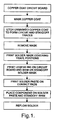
- Figure 1 is a flow chart for processing a circuit board for surface mounting an electronic component to the circuit board that includes forming a composite standoff according to the method of the invention;
- Figure 2 is a fragmentary top view of a circuit board having a composite standoff formed by the method of the invention;
- Figure 3 is a section taken substantially along the line 3-3 of figure 2 looking in the direction of the arrows; and
- Figure 4 is a sectional view of an electronic component mounted on the circuit board shown in figures 2 and 3.
- Referring now to figure 1, a flow chart for processing a circuit board and surface mounting an electronic component on the circuit board is illustrated. Briefly, a suitable nonconductive substrate typically of plastic material, is coated with a thin layer of conductive material, usually copper or a copper alloy. The thin conductive layer is then masked with a pattern that corresponds to the shapes and locations of desired electrical circuit traces and in this instance, the pattern also includes one or more bases for desired composite standoffs. The unmasked areas of the conductive layer are then etched to leave the desired electrical circuit traces and standoff bases. The mask is then removed from the electrical circuit traces and standoff bases. At this point it should be noted that the electrical circuit traces commonly include contact pads for making electrical connections to electronic components.
- Next a solder mask is applied to portions of the electrical circuit traces and standoff bases, for example by printing or spray coating the portions of the traces except for the contact pads that need solder. At this point it should be noted that the standoff bases are also covered with the solder mask to build up composite standoffs when the solder mask is applied to portions of the electrical circuit traces. The solder mask forms covers on the standoff bases that preferably completely cover the standoff bases.
- Any suitable material known in the art may be used for the solder mask. For example, a suitable material for the solder mask is 77MA that is commercially available material from Vantico. This material is a generally photoimageable, modified epoxy.
- Legend ink is then printed on the circuit board to identify the various mounting areas for the various electronic components which is a well known processing step. However, at the same time, legend ink is also printed on the covers of the composite standoffs to form shims atop the covers that provide a precise height for the composite standoffs. Any suitable legend ink known in the art may be used. Suitable legend inks are commercially available from Taiyo which is a well known company.
- Solder paste is then printed on the unmasked contact pads. The solder paste is preferably applied after the legend ink is applied to the circuit board and the covers of the composite standoffs.
- An electronic component is then placed on the solder paste atop the contact pads and on the composite standoffs. The solder is then reflowed and solidified to attach the electronic component to the circuit board.
- Figure 2 is a fragmentary top view of a
circuit board 10 having a composite standoff formed by the method of the invention. Figure 3 is a section taken substantially along the line 3-3 of figure 2 looking in the direction of the arrows. As indicated above,circuit board 10 comprises a suitablenonconductive substrate 12. Thecircuit board 10 is processed to provide a desired pattern ofelectrical circuit traces 14 andstandoff bases 16 comprising of a thin layer of copper, copper alloy or other suitable conductive material. The electrical circuit traces 14 includecontact pads 18 for making electrical connections with electronic components. In this particular example,circuit board 10 has two sets of eightcontact pads 18 for making electric electrical connections with two electronic components (not shown). - As shown in figures 2 and 3, the
typical standoff base 16 has acover 20 of solder mask material.Cover 20 preferably completely covers thestandoff base 16. As indicated above, thecover 20 is formed when the solder mask is applied to portions of the electrical circuit traces 14 (except for thecontact pads 18 that need solder) as well as the standoff base16. - Legend ink is then printed on the
circuit board 10 to identify the various mounting areas for various electronic components. For instance, the legend "ZRR1" indicated generally at 22 in figure 2 is printed near the mounting area on thecircuit board 10 for an electronic component as shown by thedashed line 24. At the same time, legend ink is also printed on thecover 20 of the standoff to provide ashim 26 that finishes thecomposite standoff 27 providing a precise and controllable height for thecomposite standoff 27. It should be noted that legend ink has a relatively high viscosity in comparison to solder and that the legend ink is applied by a printing process that can be localized. Consequently, the form, shape and height of the shim can be controlled in a precise manner by varying the printing process parameters such as number of prints, emulsion thickness, and curing process. Hence a precise and controllable height is achievable. -
Solder paste 28 is printed on thecontact pads 18 as shown in figure 4. The solder paste is preferably applied tocontract pads 18 after the legend ink is applied to thecircuit board 10 and thecomposite standoffs 27. In this manner, the legend ink can be applied by the manufacturer of the printed circuit board while the solder paste can be applied at another manufacturing facility, for instance at the manufacturing facility of the printed circuit board customer. - An
electronic component 30 is then placed on thesolder paste 28 atop thecontact pads 18 and on thecomposite standoff 27 that is midway between thecontact pads 18. Thesolder paste 28 is then reflowed and solidified to attach anelectronic component 30 tocircuit board 12 as shown in figure 4. - Thus the method of the invention forms a composite standoff of precise height for locating the electronic component 30 a precise distance above the
circuit board 10 without requiring any additional steps during the processing of thecircuit board 10. Withcomposite shim 26, the solder standoff height of electronic components can be increased easily to increase the solder joint life expectancy. - While the
composite standoff 27 is illustrated as having awavy shim 26 it should be understood that theshim 26 can take many shapes and forms. Forinstance shim 26 could be a single strip line, a double line or a plurality of staggered dots. Moreover, while thecomposite standoff 27 is illustrated as a single linear standoff midway between two rows ofcontact pads 18, it should be understood, that any number and/or shapes of standoffs can be formed. For instance, the four corner standoffs shown inU.S. Patent 5,056,215 cited above could be formed as composite standoffs by the method of the invention. - In other words, it will be readily understood by those persons skilled in the art that the present invention is susceptible of broad utility and application. Many embodiments and adaptations of the present invention other than those described above, as well as many variations, modifications and equivalent arrangements, will be apparent from or reasonably suggested by the present invention and the foregoing description, without departing from the substance or scope of the present invention. Accordingly, while the present invention has been described herein in detail in relation to its preferred embodiment, it is to be understood that this disclosure is only illustrative and exemplary of the present invention and is made merely for purposes of providing a full and enabling disclosure of the invention. The foregoing disclosure is not intended or to be construed to limit the present invention or otherwise to exclude any such other embodiments, adaptations, variations, modifications and equivalent arrangements, the present invention being limited only by the following claims and the equivalents thereof.
Claims (3)
- A method of forming a composite standoff on a circuit board 12 during the processing of the circuit board comprising:forming a conductive standoff base 16 while forming an electrical circuit trace 14 of the same material on the circuit board,forming a cover 20 on the conductive standoff base by applying a solder mask to the standoff base while applying a solder mask of the same material to at least a portion of the electrical circuit trace, andapplying legend ink to the cover formed by applying solder mask to the standoff base to complete a composite standoff of precise height while applying legend ink to the circuit board for locating components on the circuit board so that the composite standoff is formed without any need for an additional process step.
- The method of claim 1 wherein the electrical circuit trace 14 is spaced from the conductive standoff base 16 and includes a contact pad 18 and the solder is not applied to the contact pad.
- The method of claim 1 or 2 wherein a plurality of conductive standoff bases 16 are formed while forming an array of electrical circuit traces 14 of the same material on the circuit board simultaneously, the array of electrical circuit traces 14 being spaced from the plurality of conductive standoff bases 16 and including sets of contact pads 18;
the covers 20 are formed on the conductive standoff bases by applying the solder mask to the standoff bases while applying the solder mask of the same material to at least portions of the electrical circuit traces but not to the contact pads, and
the legend ink is applied to the covers 20 to complete composite standoffs of precise height while applying the legend ink to the circuit board for locating components on the circuit board so that the composite standoffs are formed without any need for an additional process step.
Applications Claiming Priority (1)
| Application Number | Priority Date | Filing Date | Title |
|---|---|---|---|
| US11/287,962 US20070119911A1 (en) | 2005-11-28 | 2005-11-28 | Method of forming a composite standoff on a circuit board |
Publications (1)
| Publication Number | Publication Date |
|---|---|
| EP1791406A1 true EP1791406A1 (en) | 2007-05-30 |
Family
ID=37686051
Family Applications (1)
| Application Number | Title | Priority Date | Filing Date |
|---|---|---|---|
| EP06077047A Withdrawn EP1791406A1 (en) | 2005-11-28 | 2006-11-17 | Method of forming a composite standoff on a ciruit board |
Country Status (2)
| Country | Link |
|---|---|
| US (1) | US20070119911A1 (en) |
| EP (1) | EP1791406A1 (en) |
Cited By (1)
| Publication number | Priority date | Publication date | Assignee | Title |
|---|---|---|---|---|
| JP2009278121A (en) * | 2009-07-10 | 2009-11-26 | Suzuka Fuji Xerox Co Ltd | Printed circuit board device |
Families Citing this family (4)
| Publication number | Priority date | Publication date | Assignee | Title |
|---|---|---|---|---|
| JP2009049258A (en) * | 2007-08-22 | 2009-03-05 | Nippon Dempa Kogyo Co Ltd | Electronic component mounting method |
| US9723725B2 (en) * | 2013-05-29 | 2017-08-01 | Finisar Corporation | Rigid-flexible circuit interconnects |
| JP2015109409A (en) | 2013-10-25 | 2015-06-11 | 株式会社村田製作所 | Electronic component |
| US20190067232A1 (en) * | 2017-08-31 | 2019-02-28 | Micron Technology, Inc. | Method for Solder Bridging Elimination for Bulk Solder C2S Interconnects |
Citations (3)
| Publication number | Priority date | Publication date | Assignee | Title |
|---|---|---|---|---|
| JPH05327163A (en) * | 1992-05-20 | 1993-12-10 | Fujitsu Ltd | Electronic component mounting structure |
| EP1073322A1 (en) * | 1999-07-29 | 2001-01-31 | Delphi Technologies, Inc. | A method of extending life expectancy of surface mount components |
| JP2001257445A (en) * | 2000-03-10 | 2001-09-21 | Mitsubishi Electric Corp | Printed wiring board |
Family Cites Families (14)
| Publication number | Priority date | Publication date | Assignee | Title |
|---|---|---|---|---|
| US3266125A (en) * | 1962-11-13 | 1966-08-16 | Douglas Aircraft Co Inc | Method for making electrical circuit modules |
| US4280888A (en) * | 1977-10-14 | 1981-07-28 | W. R. Grace & Co. | Screen printable, UV curable opaque legend ink composition |
| JPS54105774A (en) * | 1978-02-08 | 1979-08-20 | Hitachi Ltd | Method of forming pattern on thin film hybrid integrated circuit |
| US4533455A (en) * | 1980-10-14 | 1985-08-06 | Oronzio De Nora Impianti Elettrochimici S.P.A. | Bipolar separator plate for electrochemical cells |
| US4709252A (en) * | 1982-07-16 | 1987-11-24 | The United States Of America As Represented By The Administrator, National Aeronautics And Space Administration | Integrated photo-responsive metal oxide semiconductor circuit |
| DE3686225T2 (en) * | 1985-08-14 | 1993-01-07 | Omron Tateisi Electronics Co | ASSEMBLY STRUCTURE FOR A SURFACE-MOUNTED COMPONENT TYPE AND METHOD FOR MOUNTING THIS COMPONENT TYPE ON A PCB. |
| US5056215A (en) * | 1990-12-10 | 1991-10-15 | Delco Electronics Corporation | Method of providing standoff pillars |
| US5133118A (en) * | 1991-08-06 | 1992-07-28 | Sheldahl, Inc. | Surface mounted components on flex circuits |
| US5700715A (en) * | 1994-06-14 | 1997-12-23 | Lsi Logic Corporation | Process for mounting a semiconductor device to a circuit substrate |
| US5931371A (en) * | 1997-01-16 | 1999-08-03 | Ford Motor Company | Standoff controlled interconnection |
| US6525628B1 (en) * | 1999-06-18 | 2003-02-25 | Avx Corporation | Surface mount RC array with narrow tab portions on each of the electrode plates |
| US6461881B1 (en) * | 2000-06-08 | 2002-10-08 | Micron Technology, Inc. | Stereolithographic method and apparatus for fabricating spacers for semiconductor devices and resulting structures |
| US6754551B1 (en) * | 2000-06-29 | 2004-06-22 | Printar Ltd. | Jet print apparatus and method for printed circuit board manufacturing |
| US6573122B2 (en) * | 2001-03-28 | 2003-06-03 | International Rectifier Corporation | Wafer level insulation underfill for die attach |
-
2005
- 2005-11-28 US US11/287,962 patent/US20070119911A1/en not_active Abandoned
-
2006
- 2006-11-17 EP EP06077047A patent/EP1791406A1/en not_active Withdrawn
Patent Citations (3)
| Publication number | Priority date | Publication date | Assignee | Title |
|---|---|---|---|---|
| JPH05327163A (en) * | 1992-05-20 | 1993-12-10 | Fujitsu Ltd | Electronic component mounting structure |
| EP1073322A1 (en) * | 1999-07-29 | 2001-01-31 | Delphi Technologies, Inc. | A method of extending life expectancy of surface mount components |
| JP2001257445A (en) * | 2000-03-10 | 2001-09-21 | Mitsubishi Electric Corp | Printed wiring board |
Cited By (1)
| Publication number | Priority date | Publication date | Assignee | Title |
|---|---|---|---|---|
| JP2009278121A (en) * | 2009-07-10 | 2009-11-26 | Suzuka Fuji Xerox Co Ltd | Printed circuit board device |
Also Published As
| Publication number | Publication date |
|---|---|
| US20070119911A1 (en) | 2007-05-31 |
Similar Documents
| Publication | Publication Date | Title |
|---|---|---|
| DE3125518C2 (en) | Method of making a thin wiring assembly - US Pat | |
| US5406459A (en) | Surface mounting module for an electric circuit board | |
| US4836435A (en) | Component self alignment | |
| JPH08255861A (en) | Circuit board manufacturing method and circuit inspection apparatus | |
| US20090229108A1 (en) | Methods for forming antennas using thermoforming | |
| JP2502912B2 (en) | Apparatus and method for soldering to fine pitch | |
| JPH07211995A (en) | Method and apparatus for forming impedance-controlled flexible circuit | |
| JP6778598B2 (en) | Substrate manufacturing method and substrate | |
| US6555758B1 (en) | Multiple blank for electronic components such as SAW components, and method of building up bumps, solder frames, spacers and the like | |
| KR100457029B1 (en) | Land grid array type semiconductor device and method of mounting the same | |
| US20070119911A1 (en) | Method of forming a composite standoff on a circuit board | |
| WO2014071364A1 (en) | Discrete device mounted on substrate | |
| CN216146514U (en) | Circuit board and electronic device | |
| EP0245713B1 (en) | Solder pads for use on printed circuit boards | |
| US20060118457A1 (en) | Film carrier tape for mounting electronic component | |
| JP3118509B2 (en) | Chip resistor | |
| JP3447728B2 (en) | Chip resistor | |
| JPS61118977A (en) | Multi-electrode connector construction | |
| JPH08255701A (en) | Chip-shaped electronic component | |
| JPH10189305A (en) | Square plate type chip resistor and method of manufacturing the same | |
| KR100287738B1 (en) | Surface Mount Method for Printed Circuit Boards | |
| JP3353037B2 (en) | Chip resistor | |
| JP2001257445A (en) | Printed wiring board | |
| JP2775718B2 (en) | Chip resistor and manufacturing method thereof | |
| JPS6347157B2 (en) |
Legal Events
| Date | Code | Title | Description |
|---|---|---|---|
| PUAI | Public reference made under article 153(3) epc to a published international application that has entered the european phase |
Free format text: ORIGINAL CODE: 0009012 |
|
| AK | Designated contracting states |
Kind code of ref document: A1 Designated state(s): AT BE BG CH CY CZ DE DK EE ES FI FR GB GR HU IE IS IT LI LT LU LV MC NL PL PT RO SE SI SK TR |
|
| AX | Request for extension of the european patent |
Extension state: AL BA HR MK YU |
|
| AKX | Designation fees paid | ||
| REG | Reference to a national code |
Ref country code: DE Ref legal event code: 8566 |
|
| STAA | Information on the status of an ep patent application or granted ep patent |
Free format text: STATUS: THE APPLICATION IS DEEMED TO BE WITHDRAWN |
|
| 18D | Application deemed to be withdrawn |
Effective date: 20071201 |