EP1789760B1 - Infrared source - Google Patents
Infrared source Download PDFInfo
- Publication number
- EP1789760B1 EP1789760B1 EP05779380A EP05779380A EP1789760B1 EP 1789760 B1 EP1789760 B1 EP 1789760B1 EP 05779380 A EP05779380 A EP 05779380A EP 05779380 A EP05779380 A EP 05779380A EP 1789760 B1 EP1789760 B1 EP 1789760B1
- Authority
- EP
- European Patent Office
- Prior art keywords
- membrane
- housing part
- layer
- source according
- electrical
- Prior art date
- Legal status (The legal status is an assumption and is not a legal conclusion. Google has not performed a legal analysis and makes no representation as to the accuracy of the status listed.)
- Expired - Lifetime
Links
Images





Classifications
-
- H—ELECTRICITY
- H01—ELECTRIC ELEMENTS
- H01K—ELECTRIC INCANDESCENT LAMPS
- H01K1/00—Details
- H01K1/62—One or more circuit elements structurally associated with the lamp
-
- G—PHYSICS
- G01—MEASURING; TESTING
- G01J—MEASUREMENT OF INTENSITY, VELOCITY, SPECTRAL CONTENT, POLARISATION, PHASE OR PULSE CHARACTERISTICS OF INFRARED, VISIBLE OR ULTRAVIOLET LIGHT; COLORIMETRY; RADIATION PYROMETRY
- G01J3/00—Spectrometry; Spectrophotometry; Monochromators; Measuring colours
- G01J3/02—Details
- G01J3/10—Arrangements of light sources specially adapted for spectrometry or colorimetry
- G01J3/108—Arrangements of light sources specially adapted for spectrometry or colorimetry for measurement in the infrared range
-
- H—ELECTRICITY
- H01—ELECTRIC ELEMENTS
- H01K—ELECTRIC INCANDESCENT LAMPS
- H01K1/00—Details
- H01K1/02—Incandescent bodies
- H01K1/04—Incandescent bodies characterised by the material thereof
-
- H—ELECTRICITY
- H01—ELECTRIC ELEMENTS
- H01K—ELECTRIC INCANDESCENT LAMPS
- H01K1/00—Details
- H01K1/02—Incandescent bodies
- H01K1/16—Electric connection thereto
-
- H—ELECTRICITY
- H01—ELECTRIC ELEMENTS
- H01K—ELECTRIC INCANDESCENT LAMPS
- H01K1/00—Details
- H01K1/18—Mountings or supports for the incandescent body
Definitions
- This invention relates to a sealed infrared radiation source, comprising an emitter comprising a thin structure, e.g. a membrane or thin band, being stimulated by an electrical current conducted through said membrane, said membrane thus comprising an electrical conductor.
- a sealed infrared radiation source comprising an emitter comprising a thin structure, e.g. a membrane or thin band, being stimulated by an electrical current conducted through said membrane, said membrane thus comprising an electrical conductor.
- US 5,285,131 describes an infrared source in the 2 micron IR range comprising a membrane being encased hermetically by the substrate and a silicon nitride window.
- the emitter membrane is doped with boron to increase the efficiency of the IR emission from the source.
- the solution described in this patent comprises electrical coupling of the power supply to the source through layers of metallized aluminium, which complicated the production and sealing of the casing.
- a similar solution is shown in US 5,955,839 . Both these solutions have the disadvantage of being complicated to produce, as they comprise several different materials, Other examples are shown in US 5,814,870 and 6,204,083 .
- the source should be sealed using ordinary bonding techniques to withstand both temperature variations and other strains.
- the present invention relates to a source being based on the idea of supplying current through the housing parts, the housing parts also being made from silicon and being bonded to the emitter part by fusion bonding or similar.
- the invention is more specifically described in the independent claim.
- a hermetically sealed source is provided in a very simple process, preferably a so-called fusion bonding process.
- the present invention thus provides a solution being suitable for mass production were all electrical conductor paths are lead through the whole stack.
- the source may be hermetically sealed in vacuum or in an inert gas during production and it is possible to pack e.g. 1500 sources at the time.
- Today the packing costs are as high as the costs for the source, as each chip is hand picked, glued to a can, wire bonded to the can, and a top with an IR window is welded to the can.
- the present invention gives large cost reductions.
- the emitting membrane preferably comprises a silicon layer being doped with a very high concentration of Boron or Phosphor.
- This doped area is in thermal contact with an electrical conductor layer on the emitter, but electrically insulated from the electrical conductor layer on the emitter.
- the electrical conductor layer on the emitter has sufficient resistance to serve as a heater for the highly doped silicon.
- silicon usually is semitransparent in the infrared spectrum the high doping makes the silicon opaque and therefore it emits radiation in the near infrared spectrum.
- the absorption properties of the highly doped silicon is well known in sensors and sources, e.g. as described in US 6,169,284 and US 5,827,438 .
- the preferred embodiment of the invention comprises an emitter being made from silicon and being highly doped with Boron or Phosfor, and which is in thermal contact with a resistor heating up the emitter when a current is applied to it.
- the emitter is packed in a silicon housing and being surrounded by a sealed cavity.
- emitter/radiating part and membrane are mainly regarded describing the function and the form, respectively, of the active part of the source.
- FIG 1a and 1b a top view of the emitting part of two alternative versions of the invention are illustrated.
- the emitter is provided by an EPI membrane 11 comprising a conductive polysilicon area 10.
- the membrane also comprises electrical contact areas 12,13 for providing coupling to upper and lower parts of the source housing.
- the membrane also comprises holes 14,15 for pressure equilibration between the two sides of the membrane.
- the holes are large so as to provide heat insulation between the radiating part 10 and the remaining part of the membrane.
- the emitting part 10 acts as a radiating band or strip which may be made with a chosen width depending on the intended use.
- the band shaped embodiment may provide fast response, but will have slow heat conduction away from the sensor, thus increasing the risk for over heating.
- the radiating part 10 has almost full contact with the surrounding walls, which improves the heat transfer ratio to the environment through the material.
- the source according to the invention is produced as illustrated in the accompanying drawings, figure 2-8 .
- a first silicon layer 1,4 is provided on a silicon substrate 3 and being insulated from the substrate by an oxide layer 2. Holes 5 are etched in the first silicon layer for providing pressure equilibration etc corresponding to the openings 14,15 shown in figures 1a,1b .
- a chosen part 1 of the silicon layer 4 chosen to act as emitter in the source is doped with a high concentration of Boron or Phosphor to increase the efficiency, as described above.
- an oxide layer 6 is then provided on the first silicon layer 4 and the holes 5.
- openings 7,8 are provided in the oxide layer 6.
- One of said openings 7,8 being in one of the holes 5 through the first silicon layer 4, so as to provide a hole directly through to the substrate 3.
- Another of said openings 7 is provided to obtain contact through the oxide layer 6 to the first silicon layer 4, the position of this opening not being on the highly doped part 1.
- an electrical conductive layer 9 (e.g. doped polysilicon) is provided on the first silicon layer thus also covering the holes and openings in the upper oxide layer.
- the electrically conductive layer provides electrical contact through the openings 7,8 to both the substrate 3 and at least a part of the first silicon layer 4.
- the electrically conductive polysilicon layer is then, see figure 6 removed from the holes 5, except from the hole being provided with the opening 8 to the substrate 3, and from other parts 21 (see figure 7 ) along the rim of first silicon layer 11.
- electrical coupling is obtained from the rim area 21, through the opening 7 to the polysilicon layer, passed the Boron or Phosphor doped emitter area 1, and through the opening 8 in a hole in the first silicon layer to the substrate 3.
- the oxide layer 6 is also removed from the rim 21 of the first silicon layer and from the holes 5 not provided with the conductive polysilicon layer, and a cavity is etched through the substrate from below up to the lower oxide layer 2 under the Boron or Phosphor doped area 1 forming the emitter area, and the holes 5.
- through-holes 14 are obtained connecting the cavity and the upper side of the emitter.
- the emitter is left as a membrane enclosed in an oxide layer and being provided with an electrically conductive heater layer, e.g. of doped polysilicon.
- new silicon housing parts 16,17 are then laminated over and below the element, preferably using a bonding process.
- the upper housing part 16 defines a cavity and is bonded to the first silicon layer 4 along the rim 21 where the oxide layer was removed, thus providing electrical contact between the upper housing and the first silicon layer, and the lower housing part 17 is bonded to the substrate 3 thus defining a lower cavity.
- the two cavities are provided with a pressure equilibration holes between them, but are otherwise sealed, and may be filled with inert gas or vacuum to avoid oxidation.
- the lower housing part is provided with electrical contact with the electrically conductive layer of polysilicon through the hole provided with an opening in the silicon layer.
- the lower housing part is also provided with a cavity under the radiation element 1.
- Metal layers 18,19 may then be provided on the upper and lower housing parts 16,17.
- One of said metallic layers should be provided with a window 20 above the emitter area 1 so as to allow the emitted infrared radiation pass through.
- the undoped silicon material in the housing 16 is transparent to infrared radiation.
- optical elements such as a lens or diffractive optical elements are provided on or in the structure of one of the housing parts, thus shaping or focussing the infrared light emitted from the membrane.
- the diffractive optical element is especially advantageous if the light source is small or collimated, or a distance is provided between the source and the optical elements.
- a filter may also be added to modulate the wavelength distribution.
- the device is primarily meant to be mass produced with silicon, being constructed by micromachining a radiation element in a silicon wafer.
- a cavity is etched, so that the cavity is positioned above the radiation element.
- electrical contact is provided to the radiation element through the top wafer, which is coupled to an insulated epi-layer on the mid wafer, up from the epi-layer to a doped poly-Si layer extending above the radiation element 1, down from the poly-Si layer through the epi-layer but insulated therefrom and further through an insulating oxide layer to the substrate of the mid wafer and down to the bottom wafer. It is thus possible to couple directly to the top of the upper wafer and to the surface of the bottom wafer, thus to send a current through the stack for heating the radiation element When the radiation element is heated the IR radiation goes through the top wafer, which is transparent to IR because the doping level is low. The emitted radiation corresponds essentially to a grey body.
- Typical dimensions of the radiation source is as follows: The thickness of the radiation element: a few ⁇ m Length/width of the radiaton element: typically in the range from a few hundred ⁇ m to a few mm. Length/width of the chip. A couple of mm Thickness of chip Typically 1-2mm Wafer thickness: Typically 300-500 ⁇ m
- the radiation source according to the invention is possible to produce using standard process steps of semiconductor technology. Silicon wafers are for example processed using
- the emitter membrane may be subject to large temperature fluctuations it may be advantageous to the prove temperature sensors such as a temperature sensitive resistor or diode on the emitter.
- the sensor being provided with electrical conductors for coupling to the temperature measuring means monitoring the temperature of the emitter, said temperature measuring circuitry being provided in the housing or externally for monitoring the temperature of the emitter.
- Alternative other temperature measuring means may be employed to monitor the temperature of the emitting membrane, e.g. positioned in the housing.
- Other variations and alternatives may of course also be made by a person skilled in the art within the scope of this invention, such as providing the electrical contacts on the sides of the source housing or variations in the materials used to manufacture the unit.
- the emitting part 10 of the source is constituted by a conductive layer 9, e.g. polysilicon, and a doped layer 1, e.g. doped with Boron or Phosphor, being separated by an insulating layer 6.
- Fig. 10 illustrates an alternative emitter according to the invention.
- the current is lead through openings 12,13 in the doped layer and being insulated from this.
- the current is lead through the doped layer 31 and through an opening 35 in the insulating layer 34 separating it from the heater layer 32. This way the current is forced through a small area of the heater layer 32, providing a larger current in the area surrounding the opening and thus increasing the emitted IR intensity in this area.
- the source is illustrated with electrodes 33 mounted on top of the emitter, but the solution in figure 9 , with electrical contacts at the top and bottom may of course also be used with the necessary modifications, e.g. concerning the openings for leading the current to the heater layer.
- the electrodes 10 in figure 10 are ring shaped so at to provide a uniform current flow into and from the opening 35.
- the opening may be a complete removal of the insulating layer 34 or a thin layer may remain, especially when the drive current is pulsed or an AC current is provided.
Landscapes
- Physics & Mathematics (AREA)
- Spectroscopy & Molecular Physics (AREA)
- General Physics & Mathematics (AREA)
- Resistance Heating (AREA)
- Inspection Of Paper Currency And Valuable Securities (AREA)
- Carbon And Carbon Compounds (AREA)
- Telephone Function (AREA)
- Photometry And Measurement Of Optical Pulse Characteristics (AREA)
- Radiation Pyrometers (AREA)
Abstract
Description
- This invention relates to a sealed infrared radiation source, comprising an emitter comprising a thin structure, e.g. a membrane or thin band, being stimulated by an electrical current conducted through said membrane, said membrane thus comprising an electrical conductor.
- Usually sealed infrared sources have electrical conductors for supplying energy to the emitter which passes between the layers constituted by glass housings and silicon membrane layers, as is described in
US 5,591,679 . This method, however, have several disadvantages such as complicated production and temperature characteristics, -
US 5,285,131 describes an infrared source in the 2 micron IR range comprising a membrane being encased hermetically by the substrate and a silicon nitride window. The emitter membrane is doped with boron to increase the efficiency of the IR emission from the source. The solution described in this patent comprises electrical coupling of the power supply to the source through layers of metallized aluminium, which complicated the production and sealing of the casing. A similar solution is shown inUS 5,955,839 . Both these solutions have the disadvantage of being complicated to produce, as they comprise several different materials, Other examples are shown inUS 5,814,870 and6,204,083 . - The use of silicon being heavily doped with Boron or Phosphor to increase the efficiency of IR radiation of a source is known and described in
US 5,827,438 . - It is an object of this invention to provide a infrared source being possible to mass produce using silicon technology. The source should be sealed using ordinary bonding techniques to withstand both temperature variations and other strains.
- The present invention relates to a source being based on the idea of supplying current through the housing parts, the housing parts also being made from silicon and being bonded to the emitter part by fusion bonding or similar. The invention is more specifically described in the independent claim.
- Thus a hermetically sealed source is provided in a very simple process, preferably a so-called fusion bonding process. The present invention thus provides a solution being suitable for mass production were all electrical conductor paths are lead through the whole stack. Thus the source may be hermetically sealed in vacuum or in an inert gas during production and it is possible to pack e.g. 1500 sources at the time. Today the packing costs are as high as the costs for the source, as each chip is hand picked, glued to a can, wire bonded to the can, and a top with an IR window is welded to the can. Thus the present invention gives large cost reductions.
- According to a preferred embodiment of the invention the emitting membrane preferably comprises a silicon layer being doped with a very high concentration of Boron or Phosphor. This doped area is in thermal contact with an electrical conductor layer on the emitter, but electrically insulated from the electrical conductor layer on the emitter. The electrical conductor layer on the emitter has sufficient resistance to serve as a heater for the highly doped silicon. While silicon usually is semitransparent in the infrared spectrum the high doping makes the silicon opaque and therefore it emits radiation in the near infrared spectrum. The absorption properties of the highly doped silicon is well known in sensors and sources, e.g. as described in
US 6,169,284 andUS 5,827,438 . - Thus the preferred embodiment of the invention comprises an emitter being made from silicon and being highly doped with Boron or Phosfor, and which is in thermal contact with a resistor heating up the emitter when a current is applied to it. Preferably the emitter is packed in a silicon housing and being surrounded by a sealed cavity. In the wording of this specification emitter/radiating part and membrane are mainly regarded describing the function and the form, respectively, of the active part of the source.
- The invention will now be described with reference to the accompanying drawings, illustrating the invention by way of examples. It should be noted that the scales in the drawings are distorted to simplify their understanding.
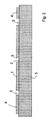
Figures 1a,b illustrates the membranes of two embodiments of the invention as seen from above. -
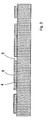
Figures 2-8 illustrates a preferred method for producing the source. -
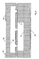
Figure 9 illustrates the function of the IR source. -
Figure 10 illustrates an alternative emitter according to the invention. - In
figure 1a and 1b a top view of the emitting part of two alternative versions of the invention are illustrated. In this case the emitter is provided by anEPI membrane 11 comprising aconductive polysilicon area 10. The membrane also compriseselectrical contact areas - The membrane also comprises
holes figure 1a the holes are large so as to provide heat insulation between theradiating part 10 and the remaining part of the membrane. In this case the emittingpart 10 acts as a radiating band or strip which may be made with a chosen width depending on the intended use. The band shaped embodiment may provide fast response, but will have slow heat conduction away from the sensor, thus increasing the risk for over heating. - In
figure 1b theradiating part 10 has almost full contact with the surrounding walls, which improves the heat transfer ratio to the environment through the material. - The source according to the invention is produced as illustrated in the accompanying drawings,
figure 2-8 . According to the preferred method of production afirst silicon layer 1,4 is provided on asilicon substrate 3 and being insulated from the substrate by anoxide layer 2.Holes 5 are etched in the first silicon layer for providing pressure equilibration etc corresponding to theopenings figures 1a,1b . A chosen part 1 of thesilicon layer 4 chosen to act as emitter in the source is doped with a high concentration of Boron or Phosphor to increase the efficiency, as described above. - In
figure 3 anoxide layer 6 is then provided on thefirst silicon layer 4 and theholes 5. - As shown in
figure 4 openings oxide layer 6. One of saidopenings holes 5 through thefirst silicon layer 4, so as to provide a hole directly through to thesubstrate 3. Another of saidopenings 7 is provided to obtain contact through theoxide layer 6 to thefirst silicon layer 4, the position of this opening not being on the highly doped part 1. - In
figure 5 an electrical conductive layer 9 (e.g. doped polysilicon) is provided on the first silicon layer thus also covering the holes and openings in the upper oxide layer. Thus the electrically conductive layer provides electrical contact through theopenings substrate 3 and at least a part of thefirst silicon layer 4. - The electrically conductive polysilicon layer is then, see
figure 6 removed from theholes 5, except from the hole being provided with theopening 8 to thesubstrate 3, and from other parts 21 (seefigure 7 ) along the rim offirst silicon layer 11. Thus electrical coupling is obtained from therim area 21, through the opening 7 to the polysilicon layer, passed the Boron or Phosphor doped emitter area 1, and through theopening 8 in a hole in the first silicon layer to thesubstrate 3. - The
oxide layer 6 is also removed from therim 21 of the first silicon layer and from theholes 5 not provided with the conductive polysilicon layer, and a cavity is etched through the substrate from below up to thelower oxide layer 2 under the Boron or Phosphor doped area 1 forming the emitter area, and theholes 5. Thus through-holes 14 are obtained connecting the cavity and the upper side of the emitter. Thus the emitter is left as a membrane enclosed in an oxide layer and being provided with an electrically conductive heater layer, e.g. of doped polysilicon. - As shown in
figure 8 newsilicon housing parts upper housing part 16 defines a cavity and is bonded to thefirst silicon layer 4 along therim 21 where the oxide layer was removed, thus providing electrical contact between the upper housing and the first silicon layer, and thelower housing part 17 is bonded to thesubstrate 3 thus defining a lower cavity. As mentioned above the two cavities are provided with a pressure equilibration holes between them, but are otherwise sealed, and may be filled with inert gas or vacuum to avoid oxidation. The lower housing part is provided with electrical contact with the electrically conductive layer of polysilicon through the hole provided with an opening in the silicon layer. According to an alternative embodiment the lower housing part is also provided with a cavity under the radiation element 1. -
Metal layers lower housing parts window 20 above the emitter area 1 so as to allow the emitted infrared radiation pass through. The undoped silicon material in thehousing 16 is transparent to infrared radiation. - An electrical current between them indicated by the
line 23 infigure 9 will then travel from the first housing part through the connection with the first silicon layer to the electrically conductive layer through the opening in the oxide layer. It then passes the electrically conductive layer provided on but insulated from the highly Boron or Phosphor doped membrane and through the hole in the first silicon layer and opening in the oxide layer to the substrate, and further to the lower housing part. Although theholes 5 are shown in the drawings these have limited sizes, se theholes figures 1a and 1b , and the electrical current path indicated byreference numeral 23 propagates around them unhindered. - Thus no separate electrical conductors are needed for providing a current to the membrane, only electrical contacts provided outside the housing. This requires only standard technology. Although the illustrated embodiment includes
electrical contact - According to an alternative embodiment of the invention optical elements, such as a lens or diffractive optical elements are provided on or in the structure of one of the housing parts, thus shaping or focussing the infrared light emitted from the membrane. The diffractive optical element is especially advantageous if the light source is small or collimated, or a distance is provided between the source and the optical elements. A filter may also be added to modulate the wavelength distribution.
- As mentioned above the device is primarily meant to be mass produced with silicon, being constructed by micromachining a radiation element in a silicon wafer. In another wafer a cavity is etched, so that the cavity is positioned above the radiation element. A third wafer, in which a cavity also may be etched, is laminated under the radiation element. The lamination may be performed using a so-called fusion bonding process, which provides a completely sealed coupling between the two.
- As illustrated in
figure 9 electrical contact is provided to the radiation element through the top wafer, which is coupled to an insulated epi-layer on the mid wafer, up from the epi-layer to a doped poly-Si layer extending above the radiation element 1, down from the poly-Si layer through the epi-layer but insulated therefrom and further through an insulating oxide layer to the substrate of the mid wafer and down to the bottom wafer. It is thus possible to couple directly to the top of the upper wafer and to the surface of the bottom wafer, thus to send a current through the stack for heating the radiation element When the radiation element is heated the IR radiation goes through the top wafer, which is transparent to IR because the doping level is low. The emitted radiation corresponds essentially to a grey body. - It should be noted that the scales of the drawings above are exaggerated, especially in the ration between height and length. Typical dimensions of the radiation source is as follows:
The thickness of the radiation element: a few µm Length/width of the radiaton element: typically in the range from a few hundred µm to a few mm. Length/width of the chip. A couple of mm Thickness of chip Typically 1-2mm Wafer thickness: Typically 300-500µm - The radiation source according to the invention is possible to produce using standard process steps of semiconductor technology. Silicon wafers are for example processed using
- photolithography,
- oxidation of silicon,
- surface depositing,
- epitaxial growth of surface layers, implanting of conductors, resistors and etch stops with suitable atoms.
- Diffusion of implanted atoms
- Etching for freeing mechanical structures, in which the etching process is stopped against doped or implanted areas.
- Processing this infrared radiation source will typically follow these steps:
- Grow highly doped silicon on a silicon substrate wafer wherein the surface silicon is insulated by an oxide.
- Grow oxide on this thin highly doped silicon layer.
- Deposit a thin polysilicon film on this oxide layer.
- Make insulated electrical contact points between the poly-silicon layer and the grown silicon layer, and between the polysilicon layer and the substrate.
- Etch a 4µm thick structure from the back
- Pattern the surface layers with standard processes.
- Etch cavities in the wafer to be bonded on top of the element wafer.
- Deposit aluminium contacts on the opposite side of the cavity.
- If applicable, etch cavities in the wafer to be laminated under the element wafer.
- Deposit aluminium contacts in the opposite side from the cavity and surface to be bonded with the element wafer.
- Laminate the three wafers with fusion bonding.
- As the emitter membrane may be subject to large temperature fluctuations it may be advantageous to the prove temperature sensors such as a temperature sensitive resistor or diode on the emitter. The sensor being provided with electrical conductors for coupling to the temperature measuring means monitoring the temperature of the emitter, said temperature measuring circuitry being provided in the housing or externally for monitoring the temperature of the emitter. Alternative other temperature measuring means may be employed to monitor the temperature of the emitting membrane, e.g. positioned in the housing. Other variations and alternatives may of course also be made by a person skilled in the art within the scope of this invention, such as providing the electrical contacts on the sides of the source housing or variations in the materials used to manufacture the unit.
- As is clear from
figure 9 the emittingpart 10 of the source is constituted by aconductive layer 9, e.g. polysilicon, and a doped layer 1, e.g. doped with Boron or Phosphor, being separated by an insulatinglayer 6. -
Fig. 10 illustrates an alternative emitter according to the invention. In the embodiments discussed above the current is lead throughopenings figure 10 the current is lead through the dopedlayer 31 and through anopening 35 in the insulatinglayer 34 separating it from theheater layer 32. This way the current is forced through a small area of theheater layer 32, providing a larger current in the area surrounding the opening and thus increasing the emitted IR intensity in this area. - In
figure 10 the source is illustrated withelectrodes 33 mounted on top of the emitter, but the solution infigure 9 , with electrical contacts at the top and bottom may of course also be used with the necessary modifications, e.g. concerning the openings for leading the current to the heater layer. Theelectrodes 10 infigure 10 are ring shaped so at to provide a uniform current flow into and from theopening 35. The opening may be a complete removal of the insulatinglayer 34 or a thin layer may remain, especially when the drive current is pulsed or an AC current is provided.
Claims (10)
- Sealed infrared radiation source, comprising an emitter membrane (1) being stimulated by an electrical current (23) conducted through said membrane, said membrane thus comprising an electrical conductor (9), wherein the membrane is mounted between a first and a second housing parts (16,17), at least one of which being transparent in the IR range, and each housing part (16,17) defining a cavity between the membrane (1) and the respective housing part of each side of the membrane, characterized in that the housing parts (16,17) are at least partially electrical conductive, and a first of said housing parts (16) is electrically coupled to a first end of said electrical conductor (9) and insulated from the second end of said electrical conductor, the second housing part (17) being electrically coupled to a second end of said electrical conductor (9) and being insulated from the first end of said electrical conductor, thus allowing a current (23) applied from the first housing part (16) to the second housing part (17) to pass through and heat said membrane (1).
- IR source according to claim 1, wherein the source is essentially constituted by three silicon parts (16,3,17) being an upper housing part (16) and a lower housing part (17) being separated by an intermediate membrane part (3), the membrane (1) being provided with an insulating material (2,6) on both sides, said insulating materials defining an opening (7) on a first side of the membrane providing electrical contact with a first housing part (16) and an opening (8) on the opposite side of the membrane for providing electrical contact with a second housing part (17),
- IR source according to claim 2, wherein the membrane (1) comprises an electrically conductive layer (9).
- IR source according to claim 3, wherein the membrane (1) comprises a highly doped (Boron or Phosphor) layer (1).
- IR source according to claim 1, wherein at least one housing part (16) is provided with an optical element (20).
- IR source according to claim 1 comprising means for measuring the temperature of the membrane.
- IR source according to claim 1,
wherein said membrane comprises an electrically conductive heater layer (9) and a highly Boron or Phosphor doped layer (1) being electrically insulated (6) from said heater layer. - IR source according to claim 7, comprising an integrated temperature sensitive resistor with electrical conductors for coupling to a temperature measuring means monitoring the temperature of said membrane.
- IR source according to claim 7, comprising an integrated temperature sensitive diode with electrical conductors for coupling to a temperature measuring means monitoring the temperature of said membrane.
- IR source according to claim 1, wherein said membrane comprises an electrically conductive heater layer (9) and a highly Boron or Phosphor doped layer (1) being separated by an insulating material (34), said insulation (34) having an opening or thinner area in the central part (35) of the emitting area, so as to allow the heating current to pass from one of said housing parts through said doped layer (31), through said opening and through a central part of said heater layer (32) to the second of said housing parts, thus providing a maximum heating and IR emission in said central membrane part.
Applications Claiming Priority (2)
| Application Number | Priority Date | Filing Date | Title |
|---|---|---|---|
| NO20043883A NO321281B1 (en) | 2004-09-15 | 2004-09-15 | Infrared source |
| PCT/NO2005/000335 WO2006031125A1 (en) | 2004-09-15 | 2005-09-13 | Infrared source |
Publications (2)
| Publication Number | Publication Date |
|---|---|
| EP1789760A1 EP1789760A1 (en) | 2007-05-30 |
| EP1789760B1 true EP1789760B1 (en) | 2010-07-14 |
Family
ID=35057610
Family Applications (1)
| Application Number | Title | Priority Date | Filing Date |
|---|---|---|---|
| EP05779380A Expired - Lifetime EP1789760B1 (en) | 2004-09-15 | 2005-09-13 | Infrared source |
Country Status (7)
| Country | Link |
|---|---|
| US (2) | US7741625B2 (en) |
| EP (1) | EP1789760B1 (en) |
| AT (1) | ATE474214T1 (en) |
| DE (1) | DE602005022323D1 (en) |
| IL (1) | IL181850A (en) |
| NO (1) | NO321281B1 (en) |
| WO (1) | WO2006031125A1 (en) |
Families Citing this family (26)
| Publication number | Priority date | Publication date | Assignee | Title |
|---|---|---|---|---|
| NO327678B1 (en) | 2007-07-17 | 2009-09-07 | Sintef Ikt | Detector system and method for detecting or determining a specific gas in a gas mixture |
| JP5223298B2 (en) * | 2007-10-30 | 2013-06-26 | 横河電機株式会社 | Infrared light source |
| US8859303B2 (en) | 2010-01-21 | 2014-10-14 | Cambridge Cmos Sensors Ltd. | IR emitter and NDIR sensor |
| US8410560B2 (en) * | 2010-01-21 | 2013-04-02 | Cambridge Cmos Sensors Ltd. | Electromigration reduction in micro-hotplates |
| US9214604B2 (en) | 2010-01-21 | 2015-12-15 | Cambridge Cmos Sensors Limited | Plasmonic IR devices |
| CN104285500B (en) | 2012-05-08 | 2017-11-28 | Ams传感器英国有限公司 | RF transmitter and NDIR sensors |
| TW201432860A (en) * | 2013-02-01 | 2014-08-16 | 眾智光電科技股份有限公司 | Wafer type infrared emitter package |
| JPWO2015045343A1 (en) * | 2013-09-26 | 2017-03-09 | パナソニックIpマネジメント株式会社 | Infrared radiation element and method of manufacturing the same |
| CN104591076B (en) * | 2015-01-07 | 2016-10-12 | 厦门大学 | A kind of infrared light supply chip based on nanostructured |
| DE102015206745B4 (en) * | 2015-04-15 | 2022-05-05 | Infineon Technologies Dresden Gmbh | Radiator and method for its manufacture |
| EP3096345B1 (en) * | 2015-05-22 | 2018-07-11 | CSEM Centre Suisse d'Electronique et de Microtechnique SA - Recherche et Développement | Infrared emitter |
| NO348540B1 (en) | 2015-10-05 | 2025-03-03 | Sintef Tto As | Infrared source |
| FR3047842B1 (en) * | 2016-02-12 | 2018-05-18 | Commissariat A L'energie Atomique Et Aux Energies Alternatives | ELECTRONIC COMPONENT WITH METALLIC RESISTANCE SUSPENDED IN A CLOSED CAVITY |
| US10393712B2 (en) * | 2016-03-22 | 2019-08-27 | Cummins Inc. | Systems and methods using a gas quality sensor |
| US10347814B2 (en) | 2016-04-01 | 2019-07-09 | Infineon Technologies Ag | MEMS heater or emitter structure for fast heating and cooling cycles |
| US10681777B2 (en) | 2016-04-01 | 2020-06-09 | Infineon Technologies Ag | Light emitter devices, optical filter structures and methods for forming light emitter devices and optical filter structures |
| FR3069707B1 (en) | 2017-07-27 | 2019-08-30 | Commissariat A L'energie Atomique Et Aux Energies Alternatives | INFRARED DEVICE |
| US10680150B2 (en) * | 2017-08-15 | 2020-06-09 | Dragan Grubisik | Electrically conductive-semitransparent solid state infrared emitter apparatus and method of use thereof |
| US10320143B2 (en) * | 2017-08-15 | 2019-06-11 | Alex Kropachev | Solid state particulate metal oxide infrared emitter apparatus and method of use thereof |
| US10636777B2 (en) * | 2017-12-22 | 2020-04-28 | Ams Sensors Uk Limited | Infra-red device |
| US10883804B2 (en) | 2017-12-22 | 2021-01-05 | Ams Sensors Uk Limited | Infra-red device |
| US10593826B2 (en) | 2018-03-28 | 2020-03-17 | Cambridge Gan Devices Limited | Infra-red devices |
| US11067422B2 (en) | 2018-03-28 | 2021-07-20 | Cambridge Gan Devices Limited | Thermal fluid flow sensor |
| US11187655B2 (en) | 2018-05-16 | 2021-11-30 | Sensera, Inc. | Compact gas sensors |
| EP3904846A1 (en) * | 2020-04-29 | 2021-11-03 | Infineon Technologies AG | Thermal emitter with embedded heating element |
| DE102021111260A1 (en) * | 2021-04-30 | 2022-11-03 | Infrasolid Gmbh | Thermal radiation source and method for measuring the exact temperature and/or radiated power of the thermal radiation source |
Family Cites Families (21)
| Publication number | Priority date | Publication date | Assignee | Title |
|---|---|---|---|---|
| EP0060609B2 (en) * | 1981-01-13 | 1994-09-28 | Mitsui Petrochemical Industries, Ltd. | Process for producing an ethylene/alpha-olefin copolymer |
| US4754141A (en) * | 1985-08-22 | 1988-06-28 | High Technology Sensors, Inc. | Modulated infrared source |
| US5285131A (en) * | 1990-12-03 | 1994-02-08 | University Of California - Berkeley | Vacuum-sealed silicon incandescent light |
| NO300078B1 (en) * | 1995-02-10 | 1997-04-01 | Sinvent As | Photo acoustic gas detector |
| US5591679A (en) | 1995-04-12 | 1997-01-07 | Sensonor A/S | Sealed cavity arrangement method |
| FI112005B (en) * | 1995-11-24 | 2003-10-15 | Valtion Teknillinen | Electrically adjustable thermal radiation source |
| DE19600306C1 (en) | 1996-01-05 | 1997-04-10 | Siemens Ag | Semiconductor component with hermetically-sealed housing for opto-electronic component |
| WO1997047159A1 (en) * | 1996-06-03 | 1997-12-11 | Kanagawa Prefectural Government | Process for producing infrared emitting device and infrared emitting device produced by the process |
| NO963924A (en) | 1996-09-19 | 1997-12-15 | Nyfotek As | Photo-acoustic infrared detector |
| US5955839A (en) * | 1997-03-26 | 1999-09-21 | Quantum Vision, Inc. | Incandescent microcavity lightsource having filament spaced from reflector at node of wave emitted |
| IT1291926B1 (en) | 1997-06-06 | 1999-01-21 | Univ Roma | INFRARED RADIATION DETECTION SYSTEM BASED ON AMORPHOUS SILICON SENSORS AND ITS ALLOYS |
| US6433338B1 (en) * | 1998-02-09 | 2002-08-13 | Tomra Systems Asa | Method and device for identification of a type of material in an object and utilization therefor |
| NO313723B1 (en) * | 1999-03-01 | 2002-11-18 | Sintef | Sensor Element |
| US6297511B1 (en) * | 1999-04-01 | 2001-10-02 | Raytheon Company | High frequency infrared emitter |
| EP1172657B1 (en) * | 2000-07-10 | 2006-08-23 | Infineon Technologies SensoNor AS | Accelerometer |
| NO315397B1 (en) | 2001-11-13 | 2003-08-25 | Sinvent As | Optical offset sensor |
| NO315396B1 (en) * | 2001-11-27 | 2003-08-25 | Vivid As | Identification System |
| NO315177B1 (en) * | 2001-11-29 | 2003-07-21 | Sinvent As | Optical offset sensor |
| NO315915B1 (en) * | 2002-02-25 | 2003-11-10 | Sintef Elektronikk Og Kybernet | Fj¶rvekt |
| JP4055697B2 (en) * | 2003-11-05 | 2008-03-05 | 株式会社デンソー | Infrared light source |
| US7279131B2 (en) * | 2004-07-01 | 2007-10-09 | Uop Llc | Method and apparatus for mass analysis of samples |
-
2004
- 2004-09-15 NO NO20043883A patent/NO321281B1/en unknown
-
2005
- 2005-09-13 WO PCT/NO2005/000335 patent/WO2006031125A1/en not_active Ceased
- 2005-09-13 EP EP05779380A patent/EP1789760B1/en not_active Expired - Lifetime
- 2005-09-13 US US11/575,218 patent/US7741625B2/en active Active
- 2005-09-13 AT AT05779380T patent/ATE474214T1/en not_active IP Right Cessation
- 2005-09-13 DE DE602005022323T patent/DE602005022323D1/en not_active Expired - Lifetime
-
2007
- 2007-03-11 IL IL181850A patent/IL181850A/en active IP Right Grant
-
2010
- 2010-05-05 US US12/774,012 patent/US7989821B2/en not_active Expired - Lifetime
Also Published As
| Publication number | Publication date |
|---|---|
| NO321281B1 (en) | 2006-04-18 |
| US20080272389A1 (en) | 2008-11-06 |
| IL181850A (en) | 2011-01-31 |
| US7741625B2 (en) | 2010-06-22 |
| IL181850A0 (en) | 2007-07-04 |
| NO20043883D0 (en) | 2004-09-15 |
| ATE474214T1 (en) | 2010-07-15 |
| US7989821B2 (en) | 2011-08-02 |
| US20100213500A1 (en) | 2010-08-26 |
| EP1789760A1 (en) | 2007-05-30 |
| WO2006031125A1 (en) | 2006-03-23 |
| DE602005022323D1 (en) | 2010-08-26 |
Similar Documents
| Publication | Publication Date | Title |
|---|---|---|
| US7989821B2 (en) | Infrared source | |
| EP0776023B1 (en) | Electrically modulatable thermal radiant source | |
| TWI497698B (en) | Infrared light emitting device | |
| CN109231154B (en) | Silicon-glass sealed black silicon surface infrared light source chip and preparation method thereof | |
| CN101432885A (en) | Front side electrical contact for photodetector array and method of making same | |
| JP3174069B2 (en) | Method of manufacturing infrared radiation element and infrared radiation element manufactured by the method | |
| JPWO1997047159A1 (en) | Method for manufacturing an infrared radiation element and an infrared radiation element manufactured by the method | |
| EP2238621B1 (en) | Lighting unit with temperature compensation | |
| TWI470670B (en) | Infrared source | |
| US20200203914A1 (en) | Molybdenum silicide / silicon nitride composite infrared emitter apparatus and method of use thereof | |
| JP2004501502A (en) | Method of manufacturing optical transmitting / receiving device, and optical transmitting / receiving device manufactured based on the method | |
| KR102328383B1 (en) | Method for manufacturing optoelectronic semiconductor chip, and optoelectronic semiconductor chip | |
| JP6988103B2 (en) | Manufacturing method of semiconductor devices, semiconductor devices | |
| JP4765663B2 (en) | Infrared communication module manufacturing method | |
| JP2008244240A (en) | Surface emitting semiconductor laser, method for manufacturing the same, and optical module | |
| US20120146069A1 (en) | Oxide Based LED BEOL Integration | |
| JP5192667B2 (en) | Light emitting device | |
| US20240297286A1 (en) | Method for producing an optoelectronic component, and optoelectronic component | |
| JP2009206217A (en) | Manufacturing method of light emitting device | |
| TW201407659A (en) | Infrared radiation device | |
| JPH06222040A (en) | Fabrication of solid electrolyte oxygen concentration sensor | |
| TW201349284A (en) | Infrared emitting device | |
| JP2009206215A (en) | Manufacturing method of light emitting device | |
| WO2000067891A2 (en) | Reflective layer buried in silicon and method of fabrication | |
| JP2000252508A (en) | Integrated photoelectric conversion device |
Legal Events
| Date | Code | Title | Description |
|---|---|---|---|
| PUAI | Public reference made under article 153(3) epc to a published international application that has entered the european phase |
Free format text: ORIGINAL CODE: 0009012 |
|
| 17P | Request for examination filed |
Effective date: 20070228 |
|
| AK | Designated contracting states |
Kind code of ref document: A1 Designated state(s): AT BE BG CH CY CZ DE DK EE ES FI FR GB GR HU IE IS IT LI LT LU LV MC NL PL PT RO SE SI SK TR |
|
| AX | Request for extension of the european patent |
Extension state: AL BA HR MK YU |
|
| RIN1 | Information on inventor provided before grant (corrected) |
Inventor name: WANG, DAG, THORSTEIN Inventor name: ROGNE, HENRIK Inventor name: MOE, SIGURD, TEODOR Inventor name: HANSEN, TROND, ANDREAS Inventor name: FERBER, ALAIN |
|
| 17Q | First examination report despatched |
Effective date: 20080312 |
|
| GRAJ | Information related to disapproval of communication of intention to grant by the applicant or resumption of examination proceedings by the epo deleted |
Free format text: ORIGINAL CODE: EPIDOSDIGR1 |
|
| GRAP | Despatch of communication of intention to grant a patent |
Free format text: ORIGINAL CODE: EPIDOSNIGR1 |
|
| GRAJ | Information related to disapproval of communication of intention to grant by the applicant or resumption of examination proceedings by the epo deleted |
Free format text: ORIGINAL CODE: EPIDOSDIGR1 |
|
| GRAP | Despatch of communication of intention to grant a patent |
Free format text: ORIGINAL CODE: EPIDOSNIGR1 |
|
| GRAJ | Information related to disapproval of communication of intention to grant by the applicant or resumption of examination proceedings by the epo deleted |
Free format text: ORIGINAL CODE: EPIDOSDIGR1 |
|
| GRAP | Despatch of communication of intention to grant a patent |
Free format text: ORIGINAL CODE: EPIDOSNIGR1 |
|
| RAP1 | Party data changed (applicant data changed or rights of an application transferred) |
Owner name: SINTEF |
|
| GRAS | Grant fee paid |
Free format text: ORIGINAL CODE: EPIDOSNIGR3 |
|
| GRAA | (expected) grant |
Free format text: ORIGINAL CODE: 0009210 |
|
| AK | Designated contracting states |
Kind code of ref document: B1 Designated state(s): AT BE BG CH CY CZ DE DK EE ES FI FR GB GR HU IE IS IT LI LT LU LV MC NL PL PT RO SE SI SK TR |
|
| AX | Request for extension of the european patent |
Extension state: AL BA HR MK YU |
|
| REG | Reference to a national code |
Ref country code: GB Ref legal event code: FG4D |
|
| REG | Reference to a national code |
Ref country code: CH Ref legal event code: EP |
|
| REG | Reference to a national code |
Ref country code: IE Ref legal event code: FG4D |
|
| REF | Corresponds to: |
Ref document number: 602005022323 Country of ref document: DE Date of ref document: 20100826 Kind code of ref document: P |
|
| REG | Reference to a national code |
Ref country code: NL Ref legal event code: VDEP Effective date: 20100714 |
|
| LTIE | Lt: invalidation of european patent or patent extension |
Effective date: 20100714 |
|
| PG25 | Lapsed in a contracting state [announced via postgrant information from national office to epo] |
Ref country code: NL Free format text: LAPSE BECAUSE OF FAILURE TO SUBMIT A TRANSLATION OF THE DESCRIPTION OR TO PAY THE FEE WITHIN THE PRESCRIBED TIME-LIMIT Effective date: 20100714 Ref country code: LT Free format text: LAPSE BECAUSE OF FAILURE TO SUBMIT A TRANSLATION OF THE DESCRIPTION OR TO PAY THE FEE WITHIN THE PRESCRIBED TIME-LIMIT Effective date: 20100714 Ref country code: FI Free format text: LAPSE BECAUSE OF FAILURE TO SUBMIT A TRANSLATION OF THE DESCRIPTION OR TO PAY THE FEE WITHIN THE PRESCRIBED TIME-LIMIT Effective date: 20100714 Ref country code: AT Free format text: LAPSE BECAUSE OF FAILURE TO SUBMIT A TRANSLATION OF THE DESCRIPTION OR TO PAY THE FEE WITHIN THE PRESCRIBED TIME-LIMIT Effective date: 20100714 |
|
| PG25 | Lapsed in a contracting state [announced via postgrant information from national office to epo] |
Ref country code: CY Free format text: LAPSE BECAUSE OF FAILURE TO SUBMIT A TRANSLATION OF THE DESCRIPTION OR TO PAY THE FEE WITHIN THE PRESCRIBED TIME-LIMIT Effective date: 20100714 Ref country code: BG Free format text: LAPSE BECAUSE OF FAILURE TO SUBMIT A TRANSLATION OF THE DESCRIPTION OR TO PAY THE FEE WITHIN THE PRESCRIBED TIME-LIMIT Effective date: 20101014 Ref country code: IS Free format text: LAPSE BECAUSE OF FAILURE TO SUBMIT A TRANSLATION OF THE DESCRIPTION OR TO PAY THE FEE WITHIN THE PRESCRIBED TIME-LIMIT Effective date: 20101114 Ref country code: PL Free format text: LAPSE BECAUSE OF FAILURE TO SUBMIT A TRANSLATION OF THE DESCRIPTION OR TO PAY THE FEE WITHIN THE PRESCRIBED TIME-LIMIT Effective date: 20100714 Ref country code: PT Free format text: LAPSE BECAUSE OF FAILURE TO SUBMIT A TRANSLATION OF THE DESCRIPTION OR TO PAY THE FEE WITHIN THE PRESCRIBED TIME-LIMIT Effective date: 20101115 Ref country code: SI Free format text: LAPSE BECAUSE OF FAILURE TO SUBMIT A TRANSLATION OF THE DESCRIPTION OR TO PAY THE FEE WITHIN THE PRESCRIBED TIME-LIMIT Effective date: 20100714 |
|
| PG25 | Lapsed in a contracting state [announced via postgrant information from national office to epo] |
Ref country code: BE Free format text: LAPSE BECAUSE OF FAILURE TO SUBMIT A TRANSLATION OF THE DESCRIPTION OR TO PAY THE FEE WITHIN THE PRESCRIBED TIME-LIMIT Effective date: 20100714 Ref country code: GR Free format text: LAPSE BECAUSE OF FAILURE TO SUBMIT A TRANSLATION OF THE DESCRIPTION OR TO PAY THE FEE WITHIN THE PRESCRIBED TIME-LIMIT Effective date: 20101015 Ref country code: SE Free format text: LAPSE BECAUSE OF FAILURE TO SUBMIT A TRANSLATION OF THE DESCRIPTION OR TO PAY THE FEE WITHIN THE PRESCRIBED TIME-LIMIT Effective date: 20100714 Ref country code: LV Free format text: LAPSE BECAUSE OF FAILURE TO SUBMIT A TRANSLATION OF THE DESCRIPTION OR TO PAY THE FEE WITHIN THE PRESCRIBED TIME-LIMIT Effective date: 20100714 |
|
| PG25 | Lapsed in a contracting state [announced via postgrant information from national office to epo] |
Ref country code: DK Free format text: LAPSE BECAUSE OF FAILURE TO SUBMIT A TRANSLATION OF THE DESCRIPTION OR TO PAY THE FEE WITHIN THE PRESCRIBED TIME-LIMIT Effective date: 20100714 Ref country code: MC Free format text: LAPSE BECAUSE OF NON-PAYMENT OF DUE FEES Effective date: 20100930 |
|
| REG | Reference to a national code |
Ref country code: CH Ref legal event code: PL |
|
| PLBE | No opposition filed within time limit |
Free format text: ORIGINAL CODE: 0009261 |
|
| STAA | Information on the status of an ep patent application or granted ep patent |
Free format text: STATUS: NO OPPOSITION FILED WITHIN TIME LIMIT |
|
| PG25 | Lapsed in a contracting state [announced via postgrant information from national office to epo] |
Ref country code: RO Free format text: LAPSE BECAUSE OF FAILURE TO SUBMIT A TRANSLATION OF THE DESCRIPTION OR TO PAY THE FEE WITHIN THE PRESCRIBED TIME-LIMIT Effective date: 20100714 Ref country code: EE Free format text: LAPSE BECAUSE OF FAILURE TO SUBMIT A TRANSLATION OF THE DESCRIPTION OR TO PAY THE FEE WITHIN THE PRESCRIBED TIME-LIMIT Effective date: 20100714 Ref country code: SK Free format text: LAPSE BECAUSE OF FAILURE TO SUBMIT A TRANSLATION OF THE DESCRIPTION OR TO PAY THE FEE WITHIN THE PRESCRIBED TIME-LIMIT Effective date: 20100714 Ref country code: CZ Free format text: LAPSE BECAUSE OF FAILURE TO SUBMIT A TRANSLATION OF THE DESCRIPTION OR TO PAY THE FEE WITHIN THE PRESCRIBED TIME-LIMIT Effective date: 20100714 Ref country code: IT Free format text: LAPSE BECAUSE OF FAILURE TO SUBMIT A TRANSLATION OF THE DESCRIPTION OR TO PAY THE FEE WITHIN THE PRESCRIBED TIME-LIMIT Effective date: 20100714 |
|
| 26N | No opposition filed |
Effective date: 20110415 |
|
| PG25 | Lapsed in a contracting state [announced via postgrant information from national office to epo] |
Ref country code: ES Free format text: LAPSE BECAUSE OF FAILURE TO SUBMIT A TRANSLATION OF THE DESCRIPTION OR TO PAY THE FEE WITHIN THE PRESCRIBED TIME-LIMIT Effective date: 20101025 |
|
| REG | Reference to a national code |
Ref country code: DE Ref legal event code: R097 Ref document number: 602005022323 Country of ref document: DE Effective date: 20110415 |
|
| PG25 | Lapsed in a contracting state [announced via postgrant information from national office to epo] |
Ref country code: LI Free format text: LAPSE BECAUSE OF NON-PAYMENT OF DUE FEES Effective date: 20100930 Ref country code: CH Free format text: LAPSE BECAUSE OF NON-PAYMENT OF DUE FEES Effective date: 20100930 Ref country code: IE Free format text: LAPSE BECAUSE OF NON-PAYMENT OF DUE FEES Effective date: 20100913 |
|
| PG25 | Lapsed in a contracting state [announced via postgrant information from national office to epo] |
Ref country code: LU Free format text: LAPSE BECAUSE OF NON-PAYMENT OF DUE FEES Effective date: 20100913 Ref country code: HU Free format text: LAPSE BECAUSE OF FAILURE TO SUBMIT A TRANSLATION OF THE DESCRIPTION OR TO PAY THE FEE WITHIN THE PRESCRIBED TIME-LIMIT Effective date: 20110115 |
|
| PG25 | Lapsed in a contracting state [announced via postgrant information from national office to epo] |
Ref country code: TR Free format text: LAPSE BECAUSE OF FAILURE TO SUBMIT A TRANSLATION OF THE DESCRIPTION OR TO PAY THE FEE WITHIN THE PRESCRIBED TIME-LIMIT Effective date: 20100714 |
|
| REG | Reference to a national code |
Ref country code: FR Ref legal event code: PLFP Year of fee payment: 12 |
|
| REG | Reference to a national code |
Ref country code: FR Ref legal event code: PLFP Year of fee payment: 13 |
|
| REG | Reference to a national code |
Ref country code: FR Ref legal event code: PLFP Year of fee payment: 14 |
|
| REG | Reference to a national code |
Ref country code: GB Ref legal event code: 732E Free format text: REGISTERED BETWEEN 20181115 AND 20181130 |
|
| REG | Reference to a national code |
Ref country code: DE Ref legal event code: R081 Ref document number: 602005022323 Country of ref document: DE Owner name: SINTEF TTO, NO Free format text: FORMER OWNER: STIFTELSEN SINTEF, TRONDHEIM, NO Ref country code: DE Ref legal event code: R081 Ref document number: 602005022323 Country of ref document: DE Owner name: SINTEF TTO, NO Free format text: FORMER OWNER: SINTEF, TRONDHEIM, NO |
|
| PGFP | Annual fee paid to national office [announced via postgrant information from national office to epo] |
Ref country code: DE Payment date: 20240919 Year of fee payment: 20 |
|
| PGFP | Annual fee paid to national office [announced via postgrant information from national office to epo] |
Ref country code: GB Payment date: 20240918 Year of fee payment: 20 |
|
| PGFP | Annual fee paid to national office [announced via postgrant information from national office to epo] |
Ref country code: FR Payment date: 20240916 Year of fee payment: 20 |
|
| REG | Reference to a national code |
Ref country code: DE Ref legal event code: R071 Ref document number: 602005022323 Country of ref document: DE |
|
| REG | Reference to a national code |
Ref country code: GB Ref legal event code: PE20 Expiry date: 20250912 |