EP1787472B1 - Messgerät zur prüfung der low noise converter schaltspannung - Google Patents
Messgerät zur prüfung der low noise converter schaltspannung Download PDFInfo
- Publication number
- EP1787472B1 EP1787472B1 EP04776155.6A EP04776155A EP1787472B1 EP 1787472 B1 EP1787472 B1 EP 1787472B1 EP 04776155 A EP04776155 A EP 04776155A EP 1787472 B1 EP1787472 B1 EP 1787472B1
- Authority
- EP
- European Patent Office
- Prior art keywords
- voltage
- lnb
- pulse width
- width modulated
- line voltage
- Prior art date
- Legal status (The legal status is an assumption and is not a legal conclusion. Google has not performed a legal analysis and makes no representation as to the accuracy of the status listed.)
- Expired - Lifetime
Links
Images


Classifications
-
- G—PHYSICS
- G01—MEASURING; TESTING
- G01R—MEASURING ELECTRIC VARIABLES; MEASURING MAGNETIC VARIABLES
- G01R29/00—Arrangements for measuring or indicating electric quantities not covered by groups G01R19/00 - G01R27/00
- G01R29/08—Measuring electromagnetic field characteristics
- G01R29/10—Radiation diagrams of antennas
-
- G—PHYSICS
- G01—MEASURING; TESTING
- G01R—MEASURING ELECTRIC VARIABLES; MEASURING MAGNETIC VARIABLES
- G01R31/00—Arrangements for testing electric properties; Arrangements for locating electric faults; Arrangements for electrical testing characterised by what is being tested not provided for elsewhere
- G01R31/28—Testing of electronic circuits, e.g. by signal tracer
- G01R31/282—Testing of electronic circuits specially adapted for particular applications not provided for elsewhere
- G01R31/2825—Testing of electronic circuits specially adapted for particular applications not provided for elsewhere in household appliances or professional audio/video equipment
-
- G—PHYSICS
- G01—MEASURING; TESTING
- G01R—MEASURING ELECTRIC VARIABLES; MEASURING MAGNETIC VARIABLES
- G01R19/00—Arrangements for measuring currents or voltages or for indicating presence or sign thereof
- G01R19/165—Indicating that current or voltage is either above or below a predetermined value or within or outside a predetermined range of values
- G01R19/16566—Circuits and arrangements for comparing voltage or current with one or several thresholds and for indicating the result not covered by subgroups G01R19/16504, G01R19/16528, G01R19/16533
- G01R19/16576—Circuits and arrangements for comparing voltage or current with one or several thresholds and for indicating the result not covered by subgroups G01R19/16504, G01R19/16528, G01R19/16533 comparing DC or AC voltage with one threshold
-
- H—ELECTRICITY
- H03—ELECTRONIC CIRCUITRY
- H03H—IMPEDANCE NETWORKS, e.g. RESONANT CIRCUITS; RESONATORS
- H03H7/00—Multiple-port networks comprising only passive electrical elements as network components
- H03H7/01—Frequency selective two-port networks
- H03H7/12—Bandpass or bandstop filters with adjustable bandwidth and fixed centre frequency
-
- H—ELECTRICITY
- H03—ELECTRONIC CIRCUITRY
- H03K—PULSE TECHNIQUE
- H03K7/00—Modulating pulses with a continuously-variable modulating signal
- H03K7/08—Duration or width modulation ; Duty cycle modulation
Definitions
- the present invention relates to system diagnostic circuitry for antenna systems with active antenna components.
- Satellite television receiving systems usually comprise an "outdoor unit” including a dish-like receiving antenna and a “block” converter, and an “indoor unit” including a tuner and a signal processing section.
- the block converter converts the entire range ("block") of relatively high frequency RF signals transmitted by a satellite to a more manageable, lower range of frequencies.
- a conventional satellite television transmission system television information is transmitted in analog form and the RF signals transmitted by the satellite are in the C (e.g., 3.7 to 4.2 GHz) and Ku (e.g., 11.7 to 14.2 GHz) bands.
- the RF signal received from the satellite by the antenna of the receiving system are converted by the block converter to the L band (e.g., 900 to 2000 MHz).
- An RF filter section of the tuner of the indoor unit selects the one of the RF signals received from the block converter corresponding to the selected channel, and a mixer/local oscillator section of the tuner converts the selected RF signal to a lower, intermediate frequency (IF) range for filtering and demodulation.
- IF intermediate frequency
- the RF signals are transmitted by the satellite in the Ku band, and are converted by the block converter to the L band.
- the frequency range of the RF signals transmitted by the satellite is somewhat smaller (e.g., between 12.2 and 12.7 GHz) than that for the analog satellite television system, and the frequency range of RF signals produced by the block converter is accordingly somewhat smaller (e.g., between 950 and 1450 MHz).
- the television information is digitized, compressed and organized into a series or stream of data packets corresponding to respective video, audio, and data portions of the television information.
- the digital data is modulated on to a RF carrier signal in what is known as QPSK (Quaternary Phase Shift Keying) modulation and the RF signal is transmitted to a satellite in earth orbit, from which it is retransmitted back to the earth.
- QPSK Quadrature Phase Shift Keying
- phase shift modulated I and Q signals are combined and the result transmitted as a QPSK modulated RF carrier signal. Accordingly, each symbol of the modulated QPSK carrier indicates one of four logic states, i.e., 00, 01, 10 and 11
- the conversion stage of the block converter of the outdoor unit is powered by a DC voltage supplied by the indoor unit.
- the satellite television signal receivers are typically located at the subscriber's residence.
- the service provider When a problem with the system occurs, it is desirable for the service provider to be able to remotely diagnose the problems with the receiver, thereby possibly avoiding having to send a service technician to the remote location. If the problem is simple enough, instructions can be given to the subscriber, and the problem immediately remedied. If the problem is too complex for the subscriber to remedy, or there is an equipment failure, advanced information on the problem can be provided to the service technician, thereby allowing the technician to bring the required parts or equipment to the subscriber's location.
- the parameters desirable to be diagnosed remotely is the LNB line voltage.
- LNB line voltages are used to select between different signals or polarizations of signals received by the LNB. There are defined ranges for each of the two allowed voltages.
- LNB line voltage is somewhere between or very, very close to one limit of allowable voltage is more desirable than just an indication of the voltage is higher than the allowable band for the lower voltage setting.
- DE 9411425 U discloses an apparatus, which comprises two comparators for a measurement of two DC voltages.
- a reference voltage is provided via a Zener diode and a potentiometer.
- US 6,650,074 discloses an apparatus generating a varying DC voltage for operating a fan motor.
- the DC voltage is provided by using a pulse width modulated signal being filtered by a low path filter.
- EP 1244308 A1 discloses an apparatus generating a DC supply voltage, which includes a switching regulator in a first step being controlled by using a pulse width modulated signal, and includes in a second step a linear regulator. The output voltages of the switching regulator and the linear regulator are controlled by using a first and a second ADC.
- GB 2384922 discloses an apparatus with a power supply providing a DC voltage for an LNB. If the voltage level of the DC voltage is above a predefined threshold level, the LNB is deemed to be operable. If the voltage level is below the threshold level, the LNB is deemed to be inoperable, and the power supply is switched off and switched on again after a short period of time.
- the present invention concerns an LNB line voltage measurement apparatus and method, as described in the claims 1 and 4. Preferred embodiments are disclosed in the dependent claims. This and other aspects of the invention will be described in detail with reference to the accompanying drawings.
- FIG. 1 a diagram of an exemplary embodiment of a satellite television system is shown.
- Fig. 1 shows a transmitting satellite (110), a parabolic dish antenna (120) with a low noise block (130), a digital satellite set-top box (140) and a television monitor (150).
- a satellite broadcast system operates to broadcast microwave signals to a wide broadcast area. In a digital television broadcast system, this is accomplished by transmitting the signals from a geosynchronous satellite (110).
- a geosynchronous satellite (110) orbits the earth once each day and sits at approximately 35,786 kilometers above the earths surface. Since a digital television broadcast satellite (110) generally orbits around the equator it constantly remains in the same position with respect to positions on the ground. This allows a satellite receiving antenna (120) to maintain a fixed look angle.
- a digital television transmitting satellite (110) receives a signal from an uplink transmitter and then rebroadcasts the signal back to earth.
- the altitude of the transmitting satellite (110) allows subscribers in a wide geographical area to receiving the signal.
- the distance from the earth and the severe power conservation requirements of the satellite also result in a weak signal being received by the subscriber. It is therefore critical that the signal be amplified as soon as possible after it is received by the antenna. This requirement is achieved through the placement of a low noise block (LNB) (130) at the feed horn of the parabolic dish antenna (120).
- LNB low noise block
- FIG. 2 a diagram of an exemplary embodiment of a satellite television receiver configuration is shown.
- Fig. 2 shows a first LNB (210), a second LNB (220), a third LNB, a switch (240), an indoor unit (250), a first transmission cable (270), a second transmission cable (260), a third transmission cable (280) and a fourth transmission cable (280).
- the dish structure of a parabolic antenna, (120) of Fig. 1 operates in a manner to reflect an incident plane wave such that the energy from the reflected wave is focused at a point proximate to the surface of the reflector structure. This point is referred to as the focal point of the parabolic antenna.
- the distance between the reflector structure and the focal point is determined by the radius of the curve of the reflector surface.
- the reflector surface is optimally configured when all the energy focused at the focal point is in phase. This essentially occurs when the energy incident travels an identical distance from the satellite to the focal point.
- the position of the focal point can also change depending on the angle of the reflection compared to the incident wave. Exploiting this opportunity to move the focal point allows antenna designers to receive signals from multiple satellites by using a single reflector with multiple LNBs. Each LNB is placed at the resulting focal point for each of the satellite signals incident on the reflector.
- the exemplary satellite television signal receiver shown in Fig. 2 is configured to receive signals from three different satellites by using a different LNB (210, 220, 230) at each of the three resulting focal points.
- LNBs 210, 220, 230
- Each of the LNBs (210, 220, 230) operate in the same manner, therefore only the operation of the first LNB (210) will be described.
- An LNB (210) is positioned at the focal point of the reflector (120) of Fig.1 , for the satellite signal desired.
- a digital television signal that is transmitted by a satellite is typically in the Ku frequency range between 12.2 and 12.7 GHz.
- This signal from the satellite is received by a feed horn integral to the LNB (210) passed to a low noise RF amplifier where the amplitude of the signal is increased.
- the amplified signal is then downconverted to a relatively lower frequency RF signal between 950 and 1450 MHz.
- This signal is then conducted by a transmission cable (270) to a switch (240).
- the switch (240) has a plurality of inputs each connected by a separate transmission cable to a plurality of LNBs.
- the switch routes the signal from the desired LNB through a second transmission cable (260) to the indoor unit (250).
- the switch 240 has three inputs, each connected to one of three LNBs (210, 220, 230).
- a digital television receiver can operate with a single LNB, in which case no switch is required, or it can operate with a large number of LNBs, each positioned with respect to the reflector surface to receive the signal from a single satellite.
- the indoor unit provides a DC voltage to the second transmission cable (260), via the switch (240), via the first transmission cable (270), and finally to the selected LNB (210).
- the DC signal is isolated both at the indoor unit (250) and the LNB (210) by a number of low pass and high pass filters. This DC voltage is commonly referred to as the LNB line voltage.
- the satellite television signal receivers are typically located at the subscriber's residence.
- the service provider When a problem with the system occurs, it is desirable for the service provider to be able to remotely diagnose the problems with the receiver, thereby possibly avoiding having to send a service technician to the remote location. If the problem is simple enough, instructions can be given to the subscriber, and the problem immediately remedied. If the problem is too complex for the subscriber to remedy, or there is an equipment failure, advanced information on the problem can be provided to the service technician, thereby allowing the technician to bring the required parts or equipment to the subscriber's location.
- the parameters desirable to be diagnosed remotely is the LNB line voltage.
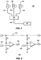
- the LNB line voltage system comprises a first comparator (320), a second comparator (330), an LNB voltage supply line (310), a first input (340), a second input (350), a first output (345) and a second output (355).
- the first input (340) of the first comparator (320) is connected to a first reference voltage.
- the LNB line voltage on the LNB voltage supply line (310) is divided using a conventional voltage divider network R1 ,R2 and compared to the first reference voltage. If the desired LNB line voltage is below the first set threshold, the first output (345) of the first comparator (320) will indicate a fault condition data bit.
- the second input (350) of the second comparator (330) is connected to a second reference voltage. If the desired LNB line voltage is below the second set threshold, the second output (355) of the second comparator (330) will indicate a fault condition data bit. Two data bits are employed indicating the output voltage is below the first threshold voltage and/or below the second threshold voltage. The two thresholds are set in the vicinity of 13 and 18 volts.
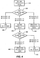
- FIG. 4 shows a test sequence followed by the system microprocessor of the indoor unit (250 of Fig. 2 ) when verification of the LNB line voltage is required.
- the system microprocessor sets the LNB line voltage to 13 volts. (410)
- the microprocessor checks the first output (345) of the first comparator (320) and the second output (355) of the second comparator (355) to ensure that the LNB line voltage exceeds 13 volts but is less than 18 volts. (420) If the two output data bits indicate that neither the 13 volt threshold has been met or the 18 volt threshold, this indicates that no 13 volt power is being supplied to the LNB, indicating a fault condition and either the subscriber or the service provider is notified.
- both the 13 volt threshold and the 18 volt threshold are exceeded, this indicates that the LNB line voltage is stuck at 18 volts indicating a fault condition and either the subscriber or the service provider is notified.
- the micro sets the LNB line voltage to 18 volts.
- the microprocessor then tests the LNB voltage to ensure that it exceeds 18 volts.
- the 13 volt threshold is exceeded but not the 18 volt threshold his indicates that no 13 volt power is being supplied to the LNB, indicating a fault condition and either the subscriber or the service provider is notified.
- both the 13 volt threshold and the 18 volt threshold are exceeded, both voltages are within desired range and the LNB voltage test is concluded. (480)
- LNB line voltage test system shown in Fig. 3
- Fig. 3 Some of the benefits of the LNB line voltage test system shown in Fig. 3 are that it requires minimal hardware and software to implement, it has reasonable accuracy over a limited range of interest, there is shared hardware over multiple LNBs.
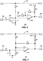
- the LNB line voltage test system shown in Fig. 5 comprises a timing capacitor C1 , a first resistor R1 , a second resistor R2, a first transistor (520), a first input (530), an LNB supply voltage line (510), a comparator (550), a third resistor R3, a fourth resistor R4, a second input (580), a third input (570) a fifth resistor R5, and an output (560).
- the LNB output voltage measurement circuit shown in Fig. 5 implements an Analog to Digital conversion method which translates the LNB power supply voltage (510) into a digital pulse, the width of which is measured by the system microprocessor.
- the microprocessor sets the first input (530) to high. This has the effect of applying a voltage to the base of the transistor (520), thereby draining any stored charge from the timing capacitor C1. Applying a voltage to the base of the transistor (520) also has the setting the collector voltage of the transistor (520) to essentially zero volts, which is the voltage seen at the inverting input of the comparator (550). Since the non inverting terminal of the comparator (550) is not higher in potential than the inverting terminal, the output (560) is set to high. To measure the LNB line voltage (510), the microprocessor sets the first input to low and captures the starts a counter.
- V C V LNB 1 ⁇ e ⁇ t / R 2 C 1
- V LNB the LNB regulator voltage being measured
- t the time to charge C1 to V ref causing the comparator (550) to transition from high to low
- Vc the LNB output voltage
- FIG. 6 shows a test sequence followed by the system microprocessor of the indoor unit (250 of Fig. 2 ) when verification of the LNB line voltage is required.
- the microprocessor sets the LNB voltage to the desired test level, either 13 or 18 volts. (610)
- the microprocessor then sets the value of the first input to zero volts.
- the microprocessor starts a counter (630), and increments that counter (640) for every cycle that the output (560) remains high (650).
- the microprocessor calculates the LNB line voltage using the counter value.
- the microprocessor compares the calculated LNB line voltage with the desired test level. (670).
- the microprocessor sets the level of the first input 530 to high 690 and returns to normal program flow. (695)
- the LNB line voltage test system shown in Fig. 7 comprises an LNB supply voltage line (710), a first input (730), a second input (720), a first output (750), a comparator (740), a first resistor R1, a second resistor R2, a third resistor R4, a fifth resistor R5, and a first capacitor C1.
- the LNB line voltage test system shown in Fig. 7 performs an analog to digital conversion of the scaled LNB line voltage (710).
- a microprocessor would be employed to produce the pulse-width modulation (PWM) signal, such as for example, the system microprocessor of the indoor unit (250 of Fig.
- PWM pulse-width modulation
- the microprocessor applies the PWM signal to the first input (730). Changing the duty cycle of pulse width modulated signal results in a lower DC value for lower duty cycles and higher DC values for higher duty cycles. At a 100% PWM duty cycle the greatest voltage possible on the inverting input of 740 is the microprocessor Vcc value. If it is desirable in the application to have the LNB voltage scaled to a value less than Vcc for comparison as in the exemplary embodiment, the first resistor R1 and the second resistor R2 make up a voltage divider to scale the LNB voltage to a comparison value below Vcc. This pulse width modulated (PWM) signal is then passed through a low pass filter C1 , R3, to convert the signal to an effective DC value.
- PWM pulse width modulated
- the comparator (740) compares the scaled LNB line voltage (710) to the DC value of the low pass filtered pulse width modulated signal.
- the comparator (740) applies an output data bit to the output (750).
- the system microprocessor of the indoor unit 250 of Fig. 2 ) then reads this output bit which indicates if the converted PWM DC value is higher or lower than the scaled LNB line voltage.
- Successive approximation, ramp method, or other methods are used to discover the closest comparison point of the scaled LNB voltage (710).
- the final percentage of pulse width modulated duty cycle is then multiplied by the pulse width modulated amplitude or system microprocessor PIO Vcc to indicate the scaled value of the measured LNB voltage (710).
- the actual LNB voltage (710) is this value multiplied by the scaling factor of the first resistor R1 and the second resistor R2.
- LNB voltage limits are read from memory accessible to the system microprocessor and the system program reports the LNB voltage status to the subscriber or the service provider.
- hysteresis is added to the comparator circuit.
- the hysteresis is achieved with the positive feedback of R4.
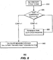
- a test sequence is shown using the ramp method of approximation which is followed by the system microprocessor of the indoor unit (250 of Fig. 2 ) when verification of the LNB line voltage is required using the circuitry shown in Fig. 7 .
- the system microprocessor of the indoor unit sets the pulse width modulated signal applied to the first input (730 of Fig. 7 ) to a 0% duty cycle.
- the microprocessor then reads the output (750 of Fig. 7 ) of the comparator (740 of Fig. 7 ). (820). If the output is low, this indicates that the scaled LNB voltage does not exceed the effective DC value of the filtered PWM signal.
- the system microprocessor increments the PWM duty cycle by a predetermined amount 830.
- the system microprocessor then rereads the output (750 of Fig. 7 ) of the comparator (740 of Fig. 7 ). (820) This process is repeated until the comparator output 750 indicates a high state. At this point, the high state of the output indicates that the scaled LNB voltage does exceeds the effective DC value of the filtered PWM signal.
- the system microprocessor then calculates the LNB line voltage based on the value of the duty cycle used during the last increment. (840).
- the measured LNB line voltage can be calculated by taking the product of the duty cycle, the PWM signal amplitude and any scaling factors.
Landscapes
- Engineering & Computer Science (AREA)
- Physics & Mathematics (AREA)
- General Physics & Mathematics (AREA)
- Multimedia (AREA)
- General Engineering & Computer Science (AREA)
- Electromagnetism (AREA)
- Power Engineering (AREA)
- Input Circuits Of Receivers And Coupling Of Receivers And Audio Equipment (AREA)
- Two-Way Televisions, Distribution Of Moving Picture Or The Like (AREA)
- Monitoring And Testing Of Transmission In General (AREA)
- Testing Electric Properties And Detecting Electric Faults (AREA)
Claims (9)
- Vorrichtung, die umfasst:eine erste Quelle einer ersten Gleichspannung eine zweite Quelle einer zweiten Gleichspannung;einen Mikroprozessor zum Erzeugen eines pulsbreitenmodulierten Signals;ein Tiefpassfilter (R3, Cl) zum Umsetzen des pulsbreitenmodulierten Signals in eine dritte Gleichspannung;einen Schalter mit einem Ausgang zum Auswählen der ersten Gleichspannung und alternativ der zweiten Gleichspannung und zum Ausgeben einer ausgewählten Gleichspannung mit einer Amplitude; undeinen Komparator (740) zum Vergleichen der ausgewählten Gleichspannung und einer dritten Gleichspannung und zum Erzeugen eines Ausgangssignals in Ansprechen auf die Differenz zwischen der ausgewählten Gleichspannung und der dritten Gleichspannung, wobeider Mikroprozessor dafür ausgelegt ist, die Eigenschaften der pulsbreitenmodulierten Signalform einzustellen, bis eine vorgegebene Beziehung zwischen dem ausgewählten Gleichspannungswert und der dritten Spannung erfüllt ist, und wobei der Mikroprozessor dafür ausgelegt ist, das Ausgangssignal des Komparators zu empfangen und unter Verwendung der Eigenschaften der pulsbreitenmodulierten Signalform die Amplitude der ausgewählten Gleichspannung zu berechnen.
- Vorrichtung nach Anspruch 1, wobei die erste Gleichspannung eine Leistungsversorgungsspannung eines rauscharmen Verstärkers ist.
- Vorrichtung nach Anspruch 1, wobei die zweite Gleichspannung eine Leistungsversorgungsspannung eines rauscharmen Verstärkers ist.
- Verfahren zum Messen der Speisespannung eines rauscharmen Verstärkers (LNB), wobei das Verfahren die folgenden Schritte umfasst:Erzeugen einer pulsbreitenmodulierten Signalform in einem Mikroprozessor und Anlegen der pulsbreitenmodulierten Signalform an einen ersten Eingang (730);Tiefpassfiltern der pulsbreitenmodulierten Signalform, um eine effektive Gleichspannung zu erzeugen;Vergleichen der effektiven Gleichspannung mit der LNB-Speisespannung mit einem Komparator, wobei die LNB-Speisespannung eine Amplitude aufweist;Einstellen der Eigenschaften der pulsbreitenmodulierten Signalform, bis eine vorgegebene Beziehung zwischen dem effektiven Gleichspannungswert und der LNB-Speisespannung erfüllt ist; undBerechnen der Amplitude der LNB-Speisespannung in dem Mikroprozessor, der das Ausgangssignal des Komparators empfängt, unter Verwendung der Eigenschaften der pulsbreitenmodulierten Signalform.
- Verfahren nach Anspruch 4, wobei der Tastgrad der pulsbreitenmodulierten Signalform eingestellt wird, bis eine vorgegebene Beziehung zwischen dem effektiven Gleichspannungswert und der LNB-Speisespannung erfüllt ist.
- Verfahren nach Anspruch 4, wobei die Amplitude der pulsbreitenmodulierten Signalform eingestellt wird, bis eine vorgegebene Beziehung zwischen dem effektiven Gleichspannungswert und der LNB-Speisespannung erfüllt ist.
- Verfahren nach Anspruch 4, wobei das pulsbreitenmodulierten Signal unter Verwendung eines Tiefpassfilters verarbeitet wird.
- Verfahren nach Anspruch 4, wobei die Schritte des Vergleichens der effektiven Gleichspannung mit der LNB-Speisespannung, wobei die LNB-Speisespannung eine Amplitude aufweist, und des Einstellens der Eigenschaften der pulsbreitenmodulierten Signalform, bis eine vorgegebene Beziehung zwischen dem effektiven Gleichspannungswert und der LNB-Speisespannung erfüllt ist, gemäß einem Rampennäherungsverfahren ausgeführt werden.
- Verfahren nach Anspruch 4, wobei das Einstellen der Eigenschaften der pulsbreitenmodulierten Signalform, bis eine vorgegebene Beziehung zwischen dem effektiven Gleichspannungswert und der LNB-Speisespannung erfüllt ist, durch sukzessive Näherung ausgeführt wird.
Applications Claiming Priority (1)
| Application Number | Priority Date | Filing Date | Title |
|---|---|---|---|
| PCT/US2004/016864 WO2005120073A1 (en) | 2004-05-27 | 2004-05-27 | Apparatus for verifying a low noise block output voltage |
Publications (2)
| Publication Number | Publication Date |
|---|---|
| EP1787472A1 EP1787472A1 (de) | 2007-05-23 |
| EP1787472B1 true EP1787472B1 (de) | 2016-03-30 |
Family
ID=34958166
Family Applications (1)
| Application Number | Title | Priority Date | Filing Date |
|---|---|---|---|
| EP04776155.6A Expired - Lifetime EP1787472B1 (de) | 2004-05-27 | 2004-05-27 | Messgerät zur prüfung der low noise converter schaltspannung |
Country Status (7)
| Country | Link |
|---|---|
| US (1) | US7719253B2 (de) |
| EP (1) | EP1787472B1 (de) |
| JP (1) | JP4583446B2 (de) |
| KR (1) | KR101074473B1 (de) |
| CN (1) | CN101023670B (de) |
| BR (1) | BRPI0418862A (de) |
| WO (1) | WO2005120073A1 (de) |
Families Citing this family (8)
| Publication number | Priority date | Publication date | Assignee | Title |
|---|---|---|---|---|
| US7367039B2 (en) * | 2003-05-22 | 2008-04-29 | The Directv Group, Inc. | System and method for evaluating callback functionality in a satellite television network |
| US7739717B1 (en) * | 2004-07-13 | 2010-06-15 | The Directv Group, Inc. | System and method for performing diagnostics for a customer IRD in a satellite television system |
| US8515342B2 (en) * | 2005-10-12 | 2013-08-20 | The Directv Group, Inc. | Dynamic current sharing in KA/KU LNB design |
| US20080102752A1 (en) * | 2006-10-30 | 2008-05-01 | The Directv Group, Inc. | Multiple satellite mobile system using multiple antennas |
| US20080111741A1 (en) * | 2006-11-10 | 2008-05-15 | The Directv Group, Inc. | Redundant mobile antenna system and method for operating the same |
| US8903306B2 (en) | 2008-09-26 | 2014-12-02 | Thomson Licensing | Method for controlling signal transmission for multiple devices |
| US8494120B2 (en) * | 2009-11-18 | 2013-07-23 | General Instrument Corporation | Detecting foreign voltage faults in telephone customer premise equipment |
| US9337946B2 (en) | 2013-03-05 | 2016-05-10 | Qualcomm Incorporated | Dual-mode low-noise block controller |
Citations (1)
| Publication number | Priority date | Publication date | Assignee | Title |
|---|---|---|---|---|
| US6650074B1 (en) * | 2002-05-29 | 2003-11-18 | Dell Products, L.P. | Fan speed controller with conditioned tachometer signal |
Family Cites Families (13)
| Publication number | Priority date | Publication date | Assignee | Title |
|---|---|---|---|---|
| JPH0445313Y2 (de) * | 1987-11-24 | 1992-10-26 | ||
| US4945465A (en) | 1988-09-15 | 1990-07-31 | U.S. Philips Corporation | Switched-mode power supply circuit |
| JPH05300064A (ja) * | 1992-04-22 | 1993-11-12 | Fujitsu Ltd | 衛星通信受信専用局システムの監視用のif分配器 |
| DE9411425U1 (de) | 1994-07-14 | 1994-09-08 | Christian Schwaiger Kg, 90579 Langenzenn | Prüfgerät für Antennenanlagen |
| JPH098686A (ja) * | 1995-06-26 | 1997-01-10 | Matsushita Electric Works Ltd | Bsチューナ一体型アンテナ装置 |
| JPH09327123A (ja) | 1996-06-06 | 1997-12-16 | Fujitsu General Ltd | Lnb用電源保護回路 |
| JP3653215B2 (ja) * | 1999-10-01 | 2005-05-25 | シャープ株式会社 | 衛星放送受信システム、ならびに衛星放送受信システムで用いられるローノイズブロックダウンコンバータおよび衛星放送受信機 |
| GB0107045D0 (en) | 2001-03-21 | 2001-05-09 | Pace Micro Tech Plc | Control system for control of power supply for lnb in broadcast data receiving system |
| CN2489526Y (zh) * | 2001-07-13 | 2002-05-01 | 安徽四创电子股份有限公司 | 用于直接广播卫星电视的数字一体化调谐器 |
| JP3873709B2 (ja) | 2001-10-26 | 2007-01-24 | ソニー株式会社 | 受信装置 |
| GB2384922B (en) | 2002-01-16 | 2005-06-22 | Pace Micro Tech Plc | Method and Apparatus for the Supply of Power to a Low Noise Block (LNB) and/or associated apparatus |
| US6693597B2 (en) * | 2002-04-23 | 2004-02-17 | The Ohio State University Research Foundation | Layout for automotive window antenna |
| GB0220291D0 (en) | 2002-08-31 | 2002-10-09 | Pace Micro Tech Plc | Power saving facility for electrical equipment |
-
2004
- 2004-05-27 EP EP04776155.6A patent/EP1787472B1/de not_active Expired - Lifetime
- 2004-05-27 KR KR1020067024706A patent/KR101074473B1/ko not_active Expired - Fee Related
- 2004-05-27 CN CN2004800431331A patent/CN101023670B/zh not_active Expired - Fee Related
- 2004-05-27 US US11/597,095 patent/US7719253B2/en not_active Expired - Fee Related
- 2004-05-27 WO PCT/US2004/016864 patent/WO2005120073A1/en not_active Ceased
- 2004-05-27 JP JP2007515016A patent/JP4583446B2/ja not_active Expired - Fee Related
- 2004-05-27 BR BRPI0418862-4A patent/BRPI0418862A/pt not_active IP Right Cessation
Patent Citations (1)
| Publication number | Priority date | Publication date | Assignee | Title |
|---|---|---|---|---|
| US6650074B1 (en) * | 2002-05-29 | 2003-11-18 | Dell Products, L.P. | Fan speed controller with conditioned tachometer signal |
Also Published As
| Publication number | Publication date |
|---|---|
| KR101074473B1 (ko) | 2011-10-17 |
| JP4583446B2 (ja) | 2010-11-17 |
| JP2008500769A (ja) | 2008-01-10 |
| US7719253B2 (en) | 2010-05-18 |
| BRPI0418862A (pt) | 2007-11-20 |
| CN101023670B (zh) | 2011-04-06 |
| EP1787472A1 (de) | 2007-05-23 |
| US20090058397A1 (en) | 2009-03-05 |
| CN101023670A (zh) | 2007-08-22 |
| KR20070059007A (ko) | 2007-06-11 |
| WO2005120073A1 (en) | 2005-12-15 |
Similar Documents
| Publication | Publication Date | Title |
|---|---|---|
| EP0475705B1 (de) | HF-Filterabgleich unter Verwendung einer digitalen Prozessoruhr | |
| US8509722B2 (en) | Frequency drift estimation for low cost outdoor unit frequency conversions and system diagnostics | |
| EP0834991A1 (de) | Verfahren zum selbsttätigen Suchen von Signalkanälen in einem Frequenzgebiet für einen Empfänger digital modulierter Signale und Empfänger zur Anwendung des Verfahrens | |
| EP1787472B1 (de) | Messgerät zur prüfung der low noise converter schaltspannung | |
| US6278485B1 (en) | Preconfigured CATV sweep testing method and apparatus | |
| CN1128092A (zh) | 用于识别信令信道的方法和装置 | |
| US7860196B2 (en) | Method and circuit for estimating in-phase/quadrature signal amplitude imbalance | |
| US20090163162A1 (en) | Direct conversion receiving architecture with an integrated tuner self alignment function | |
| US7801489B2 (en) | Method and device for measuring radio interference levels with frequency tracking | |
| EP0839410A4 (de) | Funkempfänger und verfahren zu dessen kalibrierung | |
| US6782246B1 (en) | Method for producing a test signal | |
| EP0314931A2 (de) | Verfahren und Vorrichtung zur Übertragung von Steuersignalen in Antennensystemen | |
| US4232263A (en) | Measuring installation for frequency analysis of signal levels within a large amplitude range | |
| US6792060B1 (en) | Processor having an adaptable operational frequency | |
| BRPI0418862B1 (pt) | Aparelho para verificar uma tensão de saída de bloco de baixo ruído e método de medição de uma tensão de linha lnb | |
| DE3814900A1 (de) | Empfangsverfahren und empfangs-antennensystem fuer mobilen empfang | |
| CN117855838B (zh) | 一种相控阵天线动态控制方法及系统 | |
| KR20100089165A (ko) | 시스템의 직류 옵셋 보정 장치 및 방법 | |
| US20040242176A1 (en) | Device for down-transforming the frequency of signals | |
| US6504354B1 (en) | Signal analysis apparatus having YTO yttrium-iron garnet tuned oscillator | |
| JP4237422B2 (ja) | デジタル放送波受信品質監視装置 | |
| JP2001285216A (ja) | 受信装置 | |
| JPS59186430A (ja) | 衛星用受信機 | |
| JPS63191072A (ja) | シグナルレベルメ−タ回路 | |
| Knowles | Remote controlled telemetry receiver considerations |
Legal Events
| Date | Code | Title | Description |
|---|---|---|---|
| PUAI | Public reference made under article 153(3) epc to a published international application that has entered the european phase |
Free format text: ORIGINAL CODE: 0009012 |
|
| 17P | Request for examination filed |
Effective date: 20061206 |
|
| AK | Designated contracting states |
Kind code of ref document: A1 Designated state(s): DE FR GB |
|
| DAX | Request for extension of the european patent (deleted) | ||
| RBV | Designated contracting states (corrected) |
Designated state(s): DE FR GB |
|
| 17Q | First examination report despatched |
Effective date: 20071018 |
|
| RAP1 | Party data changed (applicant data changed or rights of an application transferred) |
Owner name: THOMSON LICENSING |
|
| GRAP | Despatch of communication of intention to grant a patent |
Free format text: ORIGINAL CODE: EPIDOSNIGR1 |
|
| INTG | Intention to grant announced |
Effective date: 20151007 |
|
| RIC1 | Information provided on ipc code assigned before grant |
Ipc: G01R 31/28 20060101ALI20150928BHEP Ipc: H04N 7/20 20060101AFI20150928BHEP |
|
| GRAS | Grant fee paid |
Free format text: ORIGINAL CODE: EPIDOSNIGR3 |
|
| GRAA | (expected) grant |
Free format text: ORIGINAL CODE: 0009210 |
|
| AK | Designated contracting states |
Kind code of ref document: B1 Designated state(s): DE FR GB |
|
| REG | Reference to a national code |
Ref country code: DE Ref legal event code: R081 Ref document number: 602004048935 Country of ref document: DE Owner name: INTERDIGITAL MADISON PATENT HOLDINGS, FR Free format text: FORMER OWNER: THOMSON LICENSING, BOULOGNE BILLANCOURT, FR Ref country code: GB Ref legal event code: FG4D |
|
| REG | Reference to a national code |
Ref country code: DE Ref legal event code: R096 Ref document number: 602004048935 Country of ref document: DE |
|
| REG | Reference to a national code |
Ref country code: GB Ref legal event code: 746 Effective date: 20160420 |
|
| REG | Reference to a national code |
Ref country code: FR Ref legal event code: PLFP Year of fee payment: 13 |
|
| REG | Reference to a national code |
Ref country code: DE Ref legal event code: R084 Ref document number: 602004048935 Country of ref document: DE |
|
| REG | Reference to a national code |
Ref country code: DE Ref legal event code: R097 Ref document number: 602004048935 Country of ref document: DE |
|
| PLBE | No opposition filed within time limit |
Free format text: ORIGINAL CODE: 0009261 |
|
| STAA | Information on the status of an ep patent application or granted ep patent |
Free format text: STATUS: NO OPPOSITION FILED WITHIN TIME LIMIT |
|
| 26N | No opposition filed |
Effective date: 20170103 |
|
| REG | Reference to a national code |
Ref country code: FR Ref legal event code: PLFP Year of fee payment: 14 |
|
| REG | Reference to a national code |
Ref country code: FR Ref legal event code: PLFP Year of fee payment: 15 |
|
| REG | Reference to a national code |
Ref country code: FR Ref legal event code: TP Owner name: THOMSON LICENSING DTV, FR Effective date: 20180830 |
|
| REG | Reference to a national code |
Ref country code: GB Ref legal event code: 732E Free format text: REGISTERED BETWEEN 20180927 AND 20181005 |
|
| REG | Reference to a national code |
Ref country code: DE Ref legal event code: R082 Ref document number: 602004048935 Country of ref document: DE Representative=s name: DEHNS, DE Ref country code: DE Ref legal event code: R081 Ref document number: 602004048935 Country of ref document: DE Owner name: INTERDIGITAL MADISON PATENT HOLDINGS, FR Free format text: FORMER OWNER: THOMSON LICENSING, ISSY-LES-MOULINEAUX, FR |
|
| PGFP | Annual fee paid to national office [announced via postgrant information from national office to epo] |
Ref country code: DE Payment date: 20190418 Year of fee payment: 16 |
|
| PGFP | Annual fee paid to national office [announced via postgrant information from national office to epo] |
Ref country code: FR Payment date: 20190419 Year of fee payment: 16 |
|
| PGFP | Annual fee paid to national office [announced via postgrant information from national office to epo] |
Ref country code: GB Payment date: 20190423 Year of fee payment: 16 |
|
| REG | Reference to a national code |
Ref country code: DE Ref legal event code: R119 Ref document number: 602004048935 Country of ref document: DE |
|
| GBPC | Gb: european patent ceased through non-payment of renewal fee |
Effective date: 20200527 |
|
| PG25 | Lapsed in a contracting state [announced via postgrant information from national office to epo] |
Ref country code: GB Free format text: LAPSE BECAUSE OF NON-PAYMENT OF DUE FEES Effective date: 20200527 Ref country code: FR Free format text: LAPSE BECAUSE OF NON-PAYMENT OF DUE FEES Effective date: 20200531 |
|
| PG25 | Lapsed in a contracting state [announced via postgrant information from national office to epo] |
Ref country code: DE Free format text: LAPSE BECAUSE OF NON-PAYMENT OF DUE FEES Effective date: 20201201 |