EP1786042A1 - Light-emitting module and light-emitting system - Google Patents
Light-emitting module and light-emitting system Download PDFInfo
- Publication number
- EP1786042A1 EP1786042A1 EP05767389A EP05767389A EP1786042A1 EP 1786042 A1 EP1786042 A1 EP 1786042A1 EP 05767389 A EP05767389 A EP 05767389A EP 05767389 A EP05767389 A EP 05767389A EP 1786042 A1 EP1786042 A1 EP 1786042A1
- Authority
- EP
- European Patent Office
- Prior art keywords
- light emitting
- section
- light
- solar battery
- emitting module
- Prior art date
- Legal status (The legal status is an assumption and is not a legal conclusion. Google has not performed a legal analysis and makes no representation as to the accuracy of the status listed.)
- Withdrawn
Links
Images



Classifications
-
- H—ELECTRICITY
- H10—SEMICONDUCTOR DEVICES; ELECTRIC SOLID-STATE DEVICES NOT OTHERWISE PROVIDED FOR
- H10W—GENERIC PACKAGES, INTERCONNECTIONS, CONNECTORS OR OTHER CONSTRUCTIONAL DETAILS OF DEVICES COVERED BY CLASS H10
- H10W90/00—Package configurations
Definitions
- the present invention relates to a light emitting module and a light emitting system, more specifically a light emitting module which is combined with a visible ray transmissible solar battery, and a light emitting system comprising such a light emitting module.
- a light emitting device wherein a translucent light emitting section and a solar battery are laminated on a translucent substrate, as described in Patent Document 1; an illumination panel wherein the light receiving face of a solar battery is arranged near a panel-form light emitting body having a light emitting face so as to position the light emitting face and the light receiving face on the same plane, as described in Patent Document 2; and a solar-power-generation-used light emitting module wherein a solar power generation section and a light emitting section which emits light by electromotive force of this solar power generation section are mounted on a single planar substrate, as described in Patent Document 3.
- the translucent light emitting section and the solar battery are successively laminated so that light radiated into the solar battery is attenuated in the translucent light emitting section; thus, the device has drawbacks such that the power of the solar battery unavoidably falls.
- the solar battery which has the light emitting face
- the panel-form light emitting body which has the light emitting face, so as to position the light emitting face and the light receiving face on the same plane; thus, the illumination panel has drawbacks such that the power of the solar battery unavoidably falls because of limitation about area.
- the module has drawbacks such that limitation is imposed onto the place where the light emitting section is to be mounted.
- An object of the present invention is to solve such problems in the prior art, and provide a light emitting module which can prevent a fall in the power of a solar battery without attenuating light radiated into the solar battery, and can easily be produced, and a light emitting system comprising such a light emitting module.
- a light emitting module comprising at least a) a solar battery section including a first translucent insulating substrate, a transparent electroconductive layer, a photoelectric conversion layer, and a first metal layer, b) a first adhesive layer, c) a light emitting section including a second translucent insulating substrate, a second metal layer, and a light emitting element, d) a second adhesive layer, and e) a protective section of a third translucent substrate which are successively laminated in this order.
- a light emitting module comprising at least a) a solar battery section including a first translucent insulating substrate, a transparent electroconductive layer, a photoelectric conversion layer, and a first metal layer, b) a first adhesive layer, c) a light emitting section including a second translucent insulating substrate, a second metal layer, and a light emitting element, d) a second adhesive layer, and e) a reflective section for reflecting light from the light emitting section which are successively laminated in this order.
- a light emitting system comprising: the light emitting module according to the above-mentioned aspect of the invention; a storage battery charged by electric power that is generated in the solar battery section of the light emitting module; and a control section that is electrically connected to this storage battery and the solar battery section and the light emitting section of the light emitting module and that monitors voltage generated in the solar battery section to switch between a charging mode from the solar battery section to the storage battery and a discharging mode from the storage battery to the light emitting section.
- the solar battery section and the light emitting section are laminated.
- the solar battery section can be arranged on the sunlight receiving face side, and further the solar battery section and the light emitting section are not present on the same plane. Therefore, there disappears a fear that light radiated into the solar battery section is attenuated by the whole or a part of the light emitting section, or a limitation about the occupation area of the solar battery section. Thus, a fall in the power of the solar battery section can be prevented.
- control section monitors the voltage generated in the solar battery section, and this generated voltage is compared with a threshold voltage for judging daytime or nighttime, whereby the control section judges the charging mode from the solar battery section of the light emitting module to the storage battery and the discharging mode from the storage battery to the light emitting section of the light emitting module, which is a load. In this way, the light emitting section can be caused to emit light automatically in the nighttime.
- a solar battery section comprises a first translucent insulating substrate, a transparent electroconductive layer, a photoelectric conversion layer and a first metal layer, and is formed, for example, as follows.
- a glass substrate is used as the first translucent insulating substrate.
- a transparent electroconductive film as the transparent electroconductive layer is formed at predetermined positions. First, laser light is used to pattern the transparent electroconductive film.
- the glass substrate on which the transparent electroconductive film is formed is washed with pure water to form a first photoelectric conversion film as the photoelectric conversion layer. Thereafter, a transparent electroconductive film is formed. Next, laser light is used to pattern the photoelectric conversion film. Thereafter, a second photoelectric conversion film is formed as the photoelectric conversion layer. Laser light is used to pattern the second photoelectric conversion film. Subsequently, a transparent electroconductive film and a metal electrode film are laminated thereon to form a rear side electrode film as the first metal layer. Next, laser light is used to pattern the rear side electrode film.
- the light emitting section comprises a second transparent insulating substrate, a second metal layer, and one or more light emitting elements, and is formed, for example, as follows.
- the second transparent insulating substrate transparent PET wherein a circuit pattern as the second metal layer is beforehand formed.
- silver paste is used as the material of the circuit pattern.
- screen printing utilizing a mask is used to make the paste into the circuit pattern onto the transparent PET, and then the paste is thermally cured.
- a land pattern for mounting the chip LEDs as the light emitting elements is formed, and silver paste is printed and painted onto the land pattern.
- each of the chip LEDs is mounted so as to make both polarities of the chip LED electrically conductive through the silver paste painted onto the land pattern.
- the circuit pattern, on which the chip LEDs are mounted, on the transparent PET is allowed to stand still in a heating furnace, so as to cure the paste thermally
- a first adhesive layer for example, an EVA layer
- a second adhesive layer for example, an EVA layer
- a third transparent insulating substrate for example, a glass substrate
- a third adhesive layer and a fourth translucent insulating substrate may be further laminated successively on the side of the first translucent insulating substrate opposite to the transparent electroconductive layer side thereof.
- the light emitting section may comprise plural light emitting units. Such a structure makes it possible to make the light emitting area of the light emitting section wider.
- the reflective section of the light emitting module according to the aspect of the invention is a section for discharging light emitted in the light emitting section from the solar battery section side without leaking the light from the side opposite to the solar battery section.
- This reflective section comprises, for example, a protective section composed of a reflective layer and a third substrate.
- the light emitting system may be a system wherein the light emitting module is fitted into a frame and further a storage battery and a control section are stored in the frame.
- a structure makes it possible to package the solar-cell-attached light emitting system into a single unit.
- the light emitting system may be a system comprising a terminal box for taking out the power of the solar battery section and a terminal box for applying voltage to the light emitting section wherein these terminal boxes are fixed to a side face of the light emitting module.
- the second metal layer in the light emitting section of the light emitting module constitutes a circuit pattern for causing the light emitting element to emit light.
- This circuit pattern may be made from an electroconductive (metal) paste.
- electroconductive paste which can be cured at a temperature of 150 °C or lower and use a PET film, which is advantageous in costs, as the second translucent insulating substrate so as to form a circuit pattern on the above-mentioned substrate.
- the light emitting element may be a chip LED.
- Such a structure makes it possible to make the thickness of the light emitting module smaller than the case that a lead type LED is used.
- the chip LED may be an LED fitted to the circuit pattern through an electroconductive paste.
- an electroconductive paste which can be cured at a temperature of 150 °C or lower and use a PET film, which is advantageous in costs, as the second translucent insulating substrate so as to mount a light emitting element on the circuit pattern formed on the above-mentioned substrate.
- all of the adhesive layers in the light emitting module may each be made of a low-temperature crosslinkable EVA film.
- a plastic substrate having no heat resistance such as polycarbonate
- the third substrate may not be any substrate having translucency.
- At least one part of the solar battery section of the light emitting module may be made of a see-through type solar battery.
- This light emitting module comprises a solar battery section 1, a light emitting section 2, and a protective section 3.
- the solar battery section 1 illustrated in Figs. 1 and 2 there is used a glass substrate 4 as a first translucent insulating substrate on which a transparent electroconductive film 5 is beforehand formed.
- the transparent electroconductive film 5 as a transparent electroconductive layer is formed on a single side surface of the glass substrate 4 and end faces of the whole circumference thereof.
- laser light is used to pattern the transparent electroconductive film 5.
- YAG fundamental wave laser light is used, which is sufficiently absorbed into the transparent electroconductive film 5.
- the transparent electroconductive film 5 is separated into the form of stripes, so that separating lines 6 are formed in the transparent electroconductive film 5.
- the photoelectric conversion film 7-1 is composed of an a-Si:Hp layer, an a-Si:Hi layer, and an a-Si:Hn layer. The total thickness thereof is from 100 to 300 nm.
- a transparent electroconductive film 8 is formed.
- the transparent electroconductive film 8 for example, ZnO or ITO is used, which is good in contact property with the a-Si:Hn layer.
- the total thickness of the transparent electroconductive film 8 is from 5 to 100 nm.
- laser light is used to pattern the photoelectric conversion film 7-1.
- a YAG SHG laser is used, which has wavelength selectivity, in order to avoid damage of the transparent electroconductive film 5 based on the laser light.
- the photoelectric conversion film 7-1 is separated into the form of stripes and simultaneously the transparent electroconductive film 8 is also removed.
- separating lines 9 are formed in the photoelectric conversion film 7-1.
- the separating lines 9 are each formed at a position about 1 to 50 ⁇ m apart from each of the separating lines 6 in the transparent electroconductive 8, so as to have a width of about 50 to 200im and overlap with the latter separa ting line by a width of about 50 im.
- a photoelectric conversion film 7-2 is formed as a photoelectric conversion layer.
- the photoelectric conversion film 7-2 is composed of a ⁇ c-Si:Hp layer, a ⁇ c-Si:Hi layer, and a ⁇ c-Si:Hn layer.
- the total thickness is from 1000 to 3000 nm.
- laser light is used to pattern the photoelectric conversion film 7-2.
- a YAG SHG laser is used, which has wavelength selectivity, in order to avoid damage of the transparent electroconductive film 5 based on the laser light.
- the photoelectric conversion film 7-2 is separated into the form of stripes and simultaneously the photoelectric conversion film 7-1 and the transparent electroconductive film 8 are also removed.
- separating lines 10 are formed in the photoelectric conversion film 7-2.
- the separating lines 10 are each formed at a position about 1 to 50 im apart from each of the separating lines 9, so as to have a width of about 50 to 200im and overlap with the latter separating line by a width of about 50 im.
- a transparent electroconductive film 11 and a metal electrode film 12 are laminated, thereby forming a rear side electrode film 13 as a first metal layer.
- a transparent electroconductive film 11 for example, ZnO or ITO is used, which has a small resistivity and a high translucency.
- the metal electrode film 12 for example, Al or Ag is used, which has a high reflectivity.
- the film thickness of the transparent electrode film 11 is from about 50 to 200 nm, and the film thickness of the metal electrode film 12 is from about 500 nm to 1 im. However, the transparent electrode film 11 may be left out.
- laser light is used to pattern the rear side electrode film 13.
- a YAG SHG laser which has wavelength selectivity, in order to avoid damage of the transparent electroconductive film 5 based on the laser light and remove the photoelectric conversion film 7-1, the transparent electroconductive film 8 and the photoelectric conversion film 7-2 simultaneously.
- the laser light is radiated thereinto from the side of the glass substrate 4, the rear side electrode film 13 is separated into the form of stripes and simultaneously the photoelectric conversion film 7-1, the transparent electroconductive film 8 and the photoelectric conversion film 7-2 are also removed. As a result, separating lines 14 are formed in the rear side electrode film 13.
- the separating lines 14 are each formed at a position about 1 to 150 ⁇ m apart from each of the separating lines 10 in the photoelectric conversion film 7-2, so as to have a width of about 50 to 200 im and overlap with the latter separating line by a width of about 50 im.
- a YAG SHG laser which has wavelength selectivity, in order to avoid damage of the transparent electroconductive film 4 based on the laser light and remove the photoelectric conversion film 7-1, the transparent electroconductive film 8 and the photoelectric conversion film 7-2 simultaneously.
- the power electric area is worked to make the translucent openings 15.
- the translucent openings 15 are made perpendicularly to the separating lines 14 in the rear side electrode film 13.
- the translucent openings 15 each having a width of 0.08 mm, the total number of which is 704, are made perpendicularly to the separating lines 14 in the rear side electrode film 13 at a pitch of about 1.27 mm in the power generating areas separated into the stripes having a width of 11.09 mm.
- the patterning for making the 704 translucent openings 15 is performed, thereby making it possible to give a numerical aperture of 10% so as to form a solar battery having a substrate size of 560 mm x 930 mm and a power output of about 50 watts [W].
- the photoelectric conversion layers have a tandem structure of the a-Si:H and ic-Si:H.
- the layers may have a single structure, tandem structure or triple structure of a-Si:H, a single structure, tandem structure or triple structure of ic-Si:H, or a tandem or triple structure where these are combined.
- the see-through type solar battery has been described as one example of the solar battery.
- the solar battery may be any solar battery that can gather light, such as a light-gathering type solar battery.
- Fig. 5 illustrates an example of the arrangement of the light emitting section 2.
- illustration of electrodes of the solar battery section 1, and others is omitted.
- a member wherein four light emitting units made of the light emitting section 2 are arranged is illustrated.
- a transparent PET 17 is used as a second translucent insulating substrate on which a circuit pattern 18 is beforehand formed as a second metal layer.
- a circuit pattern 18 is beforehand formed as a second metal layer.
- silver paste which is curable by heating at 150 °C for 30 minutes is used.
- screen printing using a mask is used to form the circuit pattern 18 onto the transparent PET 17 which has a thickness of, for example, about 50 to 500 im, and then the paste is thermally cured to form the light emitting section 2.
- Fig. 3 is a plan view illustrating an example of the circuit pattern 18 of the thus-obtained light emitting section 2 according to the invention.
- Fig. 5 for example, four light emitting units, in each of which 80 chip LEDs 19 as light emitting elements are mounted onto the circuit pattern 18 in Fig. 3, are used.
- chip LEDs each having a driving voltage of 36 volts [V], a maximum consumption current of 400 milliamperes [mA], and a consumption power of 14.4 watts [W] are constructed into each light emitting unit having a size of about 260 mm x about 300 mm.
- land patterns 23/23 for mounting the chip LEDs 19 are formed, and silver paste is printed and painted onto the land patterns 23/23 at 150 °C for 30 minutes.
- each of the chip LEDs 19 is mounted to make both the polarities thereof electrically conductive through the silver paste painted onto two out of the land patterns 23/23.
- the circuit pattern, on which the chip LEDs 19 are mounted, on the transparent PET is allowed to stand still in a heating furnace having an atmospheric temperature kept at 150 °C so as to cure the paste.
- the printing step is used.
- the painting step is not limited to this step as long as the painted amount of the silver paste can be controlled.
- the method of curing the silver paste is used to bond the chip LEDs 19 onto the circuit pattern.
- a method of using a solder to solder the chips via a reflow step may be used.
- an EVA (ethylene vinyl acetate) layer 16 which is a first adhesive layer, is sandwiched between the solar battery section 1 and the light emitting section 2.
- An EVA layer 20 as a second adhesive layer having a larger thickness than the height of the chip LEDs 19 arranged in the light emitting section 2 is sandwiched between the light emitting section 2 and a glass substrate 21 as a third translucent insulating substrate for protecting this light emitting section 2.
- the resultant is kept at 130 °C for 20 minutes to melt the EVA, and then kept at 150 °C for 45 minutes to crosslink the EVA.
- the glass substrate 21 is used to protect the chip LEDs 19.
- a fluorine based resin having a high weather resistance may be used instead of this glass substrate.
- a plastic substrate having no heat resistance such as polycarbonate
- the EVA-attached substrate is kept at 120 °C for 10 minutes to melt the EVA, and then kept at 130 °C for 45 minutes to crosslink the EVA.
- the light emitting module produced as described above is a light emitting module wherein the solar battery section 1, which transmits a part of incident light while generating electric power in the daytime, and the light emitting section 2, which emits light when electric power is supplied thereto, are physically integrated with each other so that power generating areas and light emitting areas overlap; therefore, in the place where the module is installed, sure retention of the area of the light emitting section and sure retention of the area of the power generating section are compatible with each other so that the module can be installed without receiving any limitation about installation area.
- the module is combined with a solar battery or some other battery, the combination can be used in, for example, an outdoor illumination or a guide sign.
- Fig. 4 shows a black diagram of this light emitting system, and this light emitting system comprises a light emitting module 24, a storage battery 25, and a control section 26.
- this light emitting system transmits a part of incident light, and further the storage battery 25 is charged by the electric power generated in the solar battery section 1.
- the light emitting section 2 can be caused to emit light by the supply of electric power from the storage battery 25.
- the storage battery 25 may be a lead storage battery, a nickel/metal hydride battery, a lithium/ion battery or any other secondary battery, or a capacitor.
- a lead storage battery a nickel/metal hydride battery, a lithium/ion battery or any other secondary battery, or a capacitor.
- the storage battery wherein the 10 cells are connected in series, can be charged up to 42 V
- the control section 26 may be any control section as long as the section comprises a circuit capable of switching a charging mode and a discharging mode.
- the control section 26 has a function of monitoring the battery voltage of the solar battery section 1 to switch the charging mode or the discharging mode, a function of monitoring the battery level of the storage battery 25 to switch an overcharging mode or an overdischarging mode, a function of detecting a person or the like by use of infrared rays, a function of adjusting the electric power supplied to a load in the charging mode in a pulse voltage modulating output manner, or some other function.
- Fig. 6 is a sectional view taken along line A-A' in Fig. 5.
- Fig. 6 illustrates a light emitting module having the same structure as in the embodiment 1 except that besides the light emitting module of the embodiment 1 a protective section 28, as a fourth translucent insulating substrate, is formed on the side of the power generating section.
- This light emitting module is characterized in that besides the structure in Fig. 1 the protective section 28 made of, for example, glass, preferably reinforced glass, is arranged on the light receiving face side of the solar battery section 1 so as to interpose a third adhesive layer 27 therebetween.
- the protective section 28 projects outwards from the solar battery section 1 and the light emitting section 2
- the sides of the sections 1 and 2 are preferably filled with the first to third adhesive layers 16, 20 and 27, so that the side faces are each made into the form of a single plane. Details of the power generating section 1 and the light emitting section 2 are omitted.
- This light emitting module comprises a solar battery section 1, a light emitting section 2, a reflective section and a protective section 3.
- the solar battery section 1 has the same structure as in the embodiment 1.
- the light emitting section 2 basically has the same structure as in the embodiment 1; however, the place where chip LEDs 19 are arranged, and the direction of the LEDs are different from those in the embodiment 1.
- a third substrate for example, a glass substrate 21 is used as the protective section 3, and a Ag film 29, which has a high reflectivity, is formed on the surface of the glass substrate 21 by RF sputtering.
- a Ag film 29, which has a high reflectivity is used on the glass substrate 21; however, the member for reflection is not limited to this film as long as the member is a metal film.
- a method of causing a piece of metal foil such as Al foil or Ag foil to adhere through an adhesive may be used.
- the glass substrate 21 may be a substrate having no translucency It is allowable to use a colored glass, a plate made of a metal such as Al, stainless steel, gold, silver or copper, or a substrate made of wood or plastic.
- an EVA (ethylene vinyl acetate) layer 16 which has a larger thickness than the height of chip LEDs 19 arranged in the light emitting section 2 is sandwiched, as a first adhesive layer, between the solar battery section 1 and the light emitting section 2. Furthermore, an EVA layer 20 as a second adhesive layer is sandwiched between the light emitting section 2 and a third substrate, such as a glass substrate 21, for protecting this light emitting section 2. The resultant is kept at 130 °C for 20 minutes to melt the EVA, and then kept at 150 °C for 45 minutes to crosslink the EVA.
- the glass substrate 21 is used to protect the chip LEDs 19; however, instead of this, a fluorine based resin having a high weather resistance may be used.
- a plastic substrate having no heat resistance, such as polycarbonate, as the first or second translucent insulating substrate or the third substrate it is necessary to use low-temperature EVA.
- the EVA-attached substrate is kept at 120 °C for 10 minutes to melt the EVA, and then kept at 130 °C for 45 minutes to crosslink the EVA.
- the light emitting module produced as described above is a light emitting module wherein the solar battery section 1, which generates electric power in the daytime, and the light emitting section 2, which emits light when electric power is supplied thereto, are physically integrated with each other so that power generating areas and light emitting areas overlap, and further the main light-emitting direction of the LEDs is along the power generating section direction; therefore, in the place where the module is installed, sure retention of the area of the light emitting section and sure retention of the area of the power generating section are compatible with each other so that the module can be installed without receiving any limitation about installation area.
- the module is combined with a solar battery or some other battery, the combination can be used in, for example, an outdoor illumination or a guide sign.
- FIG. 8 illustrates a light emitting module having the same structure as in the embodiment 4 except that the module has an arrangement wherein the main light emitting direction of chip LEDs 19 faces the reflective section in the light emitting module of the embodiment 4 illustrated in Fig. 7.
- the solar battery section 1, which generates electric power in the daytime, and the light emitting section 2, which emits light when electric power is supplied thereto, are physically integrated with each other, there is an arrangement wherein the main light-emitting direction of the chip LEDs 19 faces the direction opposite to the power generating section 1, and the second translucent insulating substrate 17 is interposed between the power generating section 1 and the light emitting section 2, whereby the electrode 12 of the power generating section 1 and the circuit pattern 18 of the light emitting section 2 are more satisfactorily made electrically non-conductive.
- the module can be installed without receiving any limitation about installation area. Furthermore, when the module is combined with a solar battery or some other battery, the combination can be used in, for example, an outdoor illumination or a guide sign.
- an example of the place where the light emitting module is installed is a wall face of a building or the like.
- the module is used in a wall face illumination, or the module can be caused to have a display function in accordance with an arrangement where LEDs are switched on.
- the light emitting module and the light emitting system of the invention can widely be applied to small-sized or large-sized illuminations, guide signs, and others.
Landscapes
- Photovoltaic Devices (AREA)
- Led Device Packages (AREA)
Abstract
Description
- The present invention relates to a light emitting module and a light emitting system, more specifically a light emitting module which is combined with a visible ray transmissible solar battery, and a light emitting system comprising such a light emitting module.
- Hitherto, as such light emitting modules, the following are known: a light emitting device wherein a translucent light emitting section and a solar battery are laminated on a translucent substrate, as described in
Patent Document 1; an illumination panel wherein the light receiving face of a solar battery is arranged near a panel-form light emitting body having a light emitting face so as to position the light emitting face and the light receiving face on the same plane, as described inPatent Document 2; and a solar-power-generation-used light emitting module wherein a solar power generation section and a light emitting section which emits light by electromotive force of this solar power generation section are mounted on a single planar substrate, as described inPatent Document 3. -
- Patent Document 1:
Japanese Unexamined Patent Publication No. 59-217991 - Patent Document 2:
Japanese Unexamined Patent Publication No. 60-78477 - Patent Document 3:
Japanese Unexamined Patent Publication No. 2001-351418 - However, in the light emitting device described in
Patent Document 1, from its sunlight receiving face side, the translucent light emitting section and the solar battery are successively laminated so that light radiated into the solar battery is attenuated in the translucent light emitting section; thus, the device has drawbacks such that the power of the solar battery unavoidably falls. In the illumination panel described inPatent Document 2, the solar battery, which has the light emitting face, is arranged near the panel-form light emitting body, which has the light emitting face, so as to position the light emitting face and the light receiving face on the same plane; thus, the illumination panel has drawbacks such that the power of the solar battery unavoidably falls because of limitation about area. In the light emitting module described inPatent Document 3, through holes are made in the single planar substrate, wherein the solar power generation section is to be mounted on the front surface and the light emitting section, which emits light by electromotive force of this solar power generation section, is to be mounted on the rear surface; and then printed wiring, a circuit using the electromotive force of the solar battery module, and elements are mounted onto the rear surface. Thus, the module has drawbacks such that limitation is imposed onto the place where the light emitting section is to be mounted. - An object of the present invention is to solve such problems in the prior art, and provide a light emitting module which can prevent a fall in the power of a solar battery without attenuating light radiated into the solar battery, and can easily be produced, and a light emitting system comprising such a light emitting module.
- According to one aspect of the present invention, provided is a light emitting module comprising at least a) a solar battery section including a first translucent insulating substrate, a transparent electroconductive layer, a photoelectric conversion layer, and a first metal layer, b) a first adhesive layer, c) a light emitting section including a second translucent insulating substrate, a second metal layer, and a light emitting element, d) a second adhesive layer, and e) a protective section of a third translucent substrate which are successively laminated in this order. Alternatively provided is a light emitting module comprising at least a) a solar battery section including a first translucent insulating substrate, a transparent electroconductive layer, a photoelectric conversion layer, and a first metal layer, b) a first adhesive layer, c) a light emitting section including a second translucent insulating substrate, a second metal layer, and a light emitting element, d) a second adhesive layer, and e) a reflective section for reflecting light from the light emitting section which are successively laminated in this order.
- According to a different aspect of the invention, provided is a light emitting system comprising: the light emitting module according to the above-mentioned aspect of the invention; a storage battery charged by electric power that is generated in the solar battery section of the light emitting module; and a control section that is electrically connected to this storage battery and the solar battery section and the light emitting section of the light emitting module and that monitors voltage generated in the solar battery section to switch between a charging mode from the solar battery section to the storage battery and a discharging mode from the storage battery to the light emitting section.
- In the light emitting module according to the one aspect of the invention, the solar battery section and the light emitting section are laminated. However, the solar battery section can be arranged on the sunlight receiving face side, and further the solar battery section and the light emitting section are not present on the same plane. Therefore, there disappears a fear that light radiated into the solar battery section is attenuated by the whole or a part of the light emitting section, or a limitation about the occupation area of the solar battery section. Thus, a fall in the power of the solar battery section can be prevented.
- In the different aspect of the invention, the control section monitors the voltage generated in the solar battery section, and this generated voltage is compared with a threshold voltage for judging daytime or nighttime, whereby the control section judges the charging mode from the solar battery section of the light emitting module to the storage battery and the discharging mode from the storage battery to the light emitting section of the light emitting module, which is a load. In this way, the light emitting section can be caused to emit light automatically in the nighttime.
-
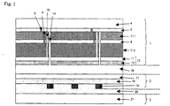
- Fig. 1 is a sectional view illustrating a light emitting module according to the invention.
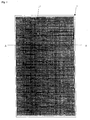
- Fig. 2 is a plan view illustrating a solar battery section in the light emitting module in Fig. 1.
- Fig. 3 is a plan view illustrating an example of a circuit pattern of a light emitting section in the light emitting module in Fig. 1.
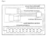
- Fig. 4 is a plan view illustrating a light emitting system according to the invention schematically.
- Fig. 5 is a plan view illustrating another light emitting module according to the invention.
- Fig. 6 is a sectional view taken along line A-A' in Fig. 5.
- Fig. 7 is a plan view illustrating still another light emitting module according to the invention.
- Fig. 8 is a plan view illustrating a different light emitting module according to the invention.
-
- 1: solar battery section
- 2: light emitting section
- 3: protective section
- 4: glass substrate (first translucent insulating substrate)
- 5: transparent electroconductive film (transparent electroconductive layer)
- 6: separating line
- 7-1: photoelectric conversion film (photoelectric conversion layer)
- 7-2: photoelectric conversion film (photoelectric conversion layer)
- 8: transparent electroconductive film
- 9: separating line
- 10: separating line
- 11: transparent electroconductive film
- 12: metal electrode film
- 13: rear side electrode film (first metal layer)
- 14: separating line
- 15: translucent opening
- 16: EVA layer (first adhesive layer)
- 17: transparent PET (second translucent insulating substrate)
- 18: circuit pattern (second metal layer)
- 19: chip LED (light emitting element)
- 20: EVA layer (second adhesive layer)
- 21: protective substrate (third substrate)
- 22: gap
- 23: land pattern
- 24: solar-cell-attached light emitting module
- 25: storage battery
- 26: control section
- 27: adhesive layer (third adhesive layer)
- 28: protective section (fourth light emitting insulating substrate)
- 29: Ag film
- In the light emitting module according to one aspect of the invention, at least the following are successively laminated: a solar battery section, a first adhesive layer, a light emitting section, a second adhesive layer, and a protective section or a reflective section.
The solar battery section comprises a first translucent insulating substrate, a transparent electroconductive layer, a photoelectric conversion layer and a first metal layer, and is formed, for example, as follows.
A glass substrate is used as the first translucent insulating substrate. On this glass substrate, a transparent electroconductive film as the transparent electroconductive layer is formed at predetermined positions.
First, laser light is used to pattern the transparent electroconductive film. Next, the glass substrate on which the transparent electroconductive film is formed is washed with pure water to form a first photoelectric conversion film as the photoelectric conversion layer. Thereafter, a transparent electroconductive film is formed.
Next, laser light is used to pattern the photoelectric conversion film. Thereafter, a second photoelectric conversion film is formed as the photoelectric conversion layer. Laser light is used to pattern the second photoelectric conversion film. Subsequently, a transparent electroconductive film and a metal electrode film are laminated thereon to form a rear side electrode film as the first metal layer. Next, laser light is used to pattern the rear side electrode film.
This way makes it possible to yield an integrated type thin film solar battery which comprises the glass substrate, the transparent electroconductive film, the first photoelectric conversion film, the transparent electroconductive film, the second photoelectric conversion film, and the rear side electrode film, and is separated into plural power generating areas connected to each other in series on the glass substrate.
The light emitting section comprises a second transparent insulating substrate, a second metal layer, and one or more light emitting elements, and is formed, for example, as follows.
There is used, as the second transparent insulating substrate, transparent PET wherein a circuit pattern as the second metal layer is beforehand formed. As the material of the circuit pattern, silver paste is used. For example, screen printing utilizing a mask is used to make the paste into the circuit pattern onto the transparent PET, and then the paste is thermally cured.
The following are used: light emitting units in each of which chip LEDs, the number of which is predetermined, as the light above-mentioned emitting elements are mounted into the circuit pattern, the number of the units being, for example, four. In each of these light emitting units, a land pattern for mounting the chip LEDs as the light emitting elements is formed, and silver paste is printed and painted onto the land pattern.
Next, each of the chip LEDs is mounted so as to make both polarities of the chip LED electrically conductive through the silver paste painted onto the land pattern. The circuit pattern, on which the chip LEDs are mounted, on the transparent PET is allowed to stand still in a heating furnace, so as to cure the paste thermally
When the solar battery section and the light emitting section, each formed in the above-mentioned way, are made into a module, a first adhesive layer (for example, an EVA layer) is sandwiched between the solar battery section and the light emitting section. Furthermore, a second adhesive layer (for example, an EVA layer) which has a larger thickness than the height of the chip LEDs arranged in the light emitting section is sandwiched between the light emitting section and a third transparent insulating substrate (for example, a glass substrate) for protecting this light emitting section. The adhesive layers are heated, so as to be melted. Thereafter, the adhesive layers are crosslinked.
In the light emitting module according to the aspect of the invention, a third adhesive layer and a fourth translucent insulating substrate may be further laminated successively on the side of the first translucent insulating substrate opposite to the transparent electroconductive layer side thereof. When the strength of the light emitting module needs to be considered, such a structure makes it possible to make the strength of the light emitting module larger by overlapping the fourth transparent insulating substrate in the state that the third adhesive layer is interposed. - In the light emitting module according to the aspect of the invention, the light emitting section may comprise plural light emitting units. Such a structure makes it possible to make the light emitting area of the light emitting section wider.
The reflective section of the light emitting module according to the aspect of the invention is a section for discharging light emitted in the light emitting section from the solar battery section side without leaking the light from the side opposite to the solar battery section. This reflective section comprises, for example, a protective section composed of a reflective layer and a third substrate. - The light emitting system according to a different aspect of the invention may be a system wherein the light emitting module is fitted into a frame and further a storage battery and a control section are stored in the frame. Such a structure makes it possible to package the solar-cell-attached light emitting system into a single unit.
- The light emitting system according to the different aspect of the invention may be a system comprising a terminal box for taking out the power of the solar battery section and a terminal box for applying voltage to the light emitting section wherein these terminal boxes are fixed to a side face of the light emitting module. Such a structure makes it possible that when the solar battery section is of a see-through type, sunlight taken therein is not blocked by the terminal box(es) or wiring which accompanies the box(es).
- In the light emitting system according to the different aspect of the invention, the second metal layer in the light emitting section of the light emitting module constitutes a circuit pattern for causing the light emitting element to emit light. This circuit pattern may be made from an electroconductive (metal) paste. Such a structure makes it possible to use an electroconductive paste which can be cured at a temperature of 150 °C or lower and use a PET film, which is advantageous in costs, as the second translucent insulating substrate so as to form a circuit pattern on the above-mentioned substrate.
- In the light emitting system according to the different aspect of the invention, the light emitting element may be a chip LED. Such a structure makes it possible to make the thickness of the light emitting module smaller than the case that a lead type LED is used.
- In the light emitting system according to the different aspect of the invention, the chip LED may be an LED fitted to the circuit pattern through an electroconductive paste. Such a structure makes it possible to use an electroconductive paste which can be cured at a temperature of 150 °C or lower and use a PET film, which is advantageous in costs, as the second translucent insulating substrate so as to mount a light emitting element on the circuit pattern formed on the above-mentioned substrate.
- In the light emitting system according to the different aspect of the invention, all of the adhesive layers in the light emitting module may each be made of a low-temperature crosslinkable EVA film. Such a structure makes it possible to use a plastic substrate having no heat resistance, such as polycarbonate, as any one of the first to fourth translucent insulating substrates and the third substrate. The third substrate may not be any substrate having translucency.
- In the light emitting system according to the different aspect of the invention, at least one part of the solar battery section of the light emitting module may be made of a see-through type solar battery. Such a structure makes it possible that at the time when this light emitting system is used in a glass window of a room or at some other time, sunlight is taken into the room from the solar battery section.
- With reference to the attached drawings, five embodiments of the invention will be described hereinafter only to show examples thereof.
- With reference to Figs. 1 to 3 and Fig. 5, an embodiment (embodiment 1) of the light emitting module according to the one aspect of the invention is described. This light emitting module comprises a
solar battery section 1, alight emitting section 2, and aprotective section 3. - In the production of the
solar battery section 1 illustrated in Figs. 1 and 2, there is used aglass substrate 4 as a first translucent insulating substrate on which atransparent electroconductive film 5 is beforehand formed. About thisglass substrate 4, thetransparent electroconductive film 5 as a transparent electroconductive layer is formed on a single side surface of theglass substrate 4 and end faces of the whole circumference thereof. - Next, laser light is used to pattern the
transparent electroconductive film 5. At this time, for example, YAG fundamental wave laser light is used, which is sufficiently absorbed into thetransparent electroconductive film 5. When the laser light is radiated thereinto from the side of theglass substrate 4, thetransparent electroconductive film 5 is separated into the form of stripes, so that separatinglines 6 are formed in thetransparent electroconductive film 5. - Next, the
glass substrate 4 on which thetransparent electroconductive film 5 is formed is washed with pure water, and then a photoelectric conversion film 7-1 is formed as a photoelectric conversion layer. The photoelectric conversion film 7-1 is composed of an a-Si:Hp layer, an a-Si:Hi layer, and an a-Si:Hn layer. The total thickness thereof is from 100 to 300 nm. - Next, a
transparent electroconductive film 8 is formed. For thetransparent electroconductive film 8, for example, ZnO or ITO is used, which is good in contact property with the a-Si:Hn layer. The total thickness of thetransparent electroconductive film 8 is from 5 to 100 nm. - Next, laser light is used to pattern the photoelectric conversion film 7-1. At this time, for example, a YAG SHG laser is used, which has wavelength selectivity, in order to avoid damage of the
transparent electroconductive film 5 based on the laser light. When the laser light is radiated thereinto from the side of theglass substrate 4, the photoelectric conversion film 7-1 is separated into the form of stripes and simultaneously thetransparent electroconductive film 8 is also removed. As a result, separatinglines 9 are formed in the photoelectric conversion film 7-1. Theseparating lines 9 are each formed at a position about 1 to 50ìm apart from each of theseparating lines 6 in thetransparent electroconductive 8, so as to have a width of about 50 to 200im and overlap with the latter separa ting line by a width of about 50 im. - Next, a photoelectric conversion film 7-2 is formed as a photoelectric conversion layer. The photoelectric conversion film 7-2 is composed of a ìc-Si:Hp layer, a ìc-Si:Hi layer, and a ìc-Si:Hn layer. The total thickness is from 1000 to 3000 nm.
- Next, laser light is used to pattern the photoelectric conversion film 7-2. At this time, for example, a YAG SHG laser is used, which has wavelength selectivity, in order to avoid damage of the
transparent electroconductive film 5 based on the laser light. When the laser light is radiated thereinto from the side of theglass substrate 4, the photoelectric conversion film 7-2 is separated into the form of stripes and simultaneously the photoelectric conversion film 7-1 and thetransparent electroconductive film 8 are also removed. As a result, separatinglines 10 are formed in the photoelectric conversion film 7-2. The separating lines 10 are each formed at a position about 1 to 50 im apart from each of theseparating lines 9, so as to have a width of about 50 to 200im and overlap with the latter separating line by a width of about 50 im. - Subsequently, a
transparent electroconductive film 11 and ametal electrode film 12 are laminated, thereby forming a rearside electrode film 13 as a first metal layer. For thetransparent electroconductive film 11, for example, ZnO or ITO is used, which has a small resistivity and a high translucency. For themetal electrode film 12, for example, Al or Ag is used, which has a high reflectivity. The film thickness of thetransparent electrode film 11 is from about 50 to 200 nm, and the film thickness of themetal electrode film 12 is from about 500 nm to 1 im. However, thetransparent electrode film 11 may be left out. - Next, laser light is used to pattern the rear
side electrode film 13.
At this time, for example, a YAG SHG laser is used, which has wavelength selectivity, in order to avoid damage of thetransparent electroconductive film 5 based on the laser light and remove the photoelectric conversion film 7-1, thetransparent electroconductive film 8 and the photoelectric conversion film 7-2 simultaneously. When the laser light is radiated thereinto from the side of theglass substrate 4, the rearside electrode film 13 is separated into the form of stripes and simultaneously the photoelectric conversion film 7-1, thetransparent electroconductive film 8 and the photoelectric conversion film 7-2 are also removed. As a result, separatinglines 14 are formed in the rearside electrode film 13. The separating lines 14 are each formed at a position about 1 to 150ìm apart from each of theseparating lines 10 in the photoelectric conversion film 7-2, so as to have a width of about 50 to 200 im and overlap with the latter separating line by a width of about 50 im. - This way makes it possible to yield an integrated type thin film solar battery comprising the
glass substrate 4, thetransparent electroconductive film 5, the photoelectric conversion film 7-1, which is composed of the amorphous silicon semiconductors, thetransparent electroconductive film 8, the photoelectric conversion film 7-2, which is composed of the crystalline silicon semiconductors, and the rearside electrode film 13, this solar battery being separated into plural power generating areas connected to each other in series on theglass substrate 4, wherein theseparating lines 14 in the rearside electrode film 13 penetrate through the rearside electrode film 13, the photoelectric conversion film 7-2, thetransparent electroconductive film 8 and the photoelectric conversion film 7-1 so as to pattern the solar battery into solar cells having the same shape. - Next, in each of the power generating areas, patterning for making
translucent openings 15 is performed. At this time, for example, a YAG SHG laser is used, which has wavelength selectivity, in order to avoid damage of thetransparent electroconductive film 4 based on the laser light and remove the photoelectric conversion film 7-1, thetransparent electroconductive film 8 and the photoelectric conversion film 7-2 simultaneously. When the laser light is radiated thereinto from the side of theglass substrate 4, the power electric area is worked to make thetranslucent openings 15. Thetranslucent openings 15 are made perpendicularly to theseparating lines 14 in the rearside electrode film 13. - In this example, the
translucent openings 15 each having a width of 0.08 mm, the total number of which is 704, are made perpendicularly to theseparating lines 14 in the rearside electrode film 13 at a pitch of about 1.27 mm in the power generating areas separated into the stripes having a width of 11.09 mm. - Accordingly, in the solar cells, the number of which is 48, the patterning for making the 704
translucent openings 15 is performed, thereby making it possible to give a numerical aperture of 10% so as to form a solar battery having a substrate size of 560 mm x 930 mm and a power output of about 50 watts [W]. - In this example, the photoelectric conversion layers have a tandem structure of the a-Si:H and ic-Si:H. However, the layers may have a single structure, tandem structure or triple structure of a-Si:H, a single structure, tandem structure or triple structure of ic-Si:H, or a tandem or triple structure where these are combined. In this example, the see-through type solar battery has been described as one example of the solar battery. However, the solar battery may be any solar battery that can gather light, such as a light-gathering type solar battery.
- The following will describe the production of the
light emitting section 2 illustrated in Figs. 1, 3 and 5. Fig. 5 illustrates an example of the arrangement of thelight emitting section 2. For convenience' sake, illustration of electrodes of thesolar battery section 1, and others is omitted. For example, a member wherein four light emitting units made of thelight emitting section 2 are arranged is illustrated. - As illustrated in Fig. 1, at the time of producing the
light emitting section 2, atransparent PET 17 is used as a second translucent insulating substrate on which acircuit pattern 18 is beforehand formed as a second metal layer. As the material of the circuit pattern, silver paste which is curable by heating at 150 °C for 30 minutes is used. For example, screen printing using a mask is used to form thecircuit pattern 18 onto thetransparent PET 17 which has a thickness of, for example, about 50 to 500 im, and then the paste is thermally cured to form thelight emitting section 2. - Fig. 3 is a plan view illustrating an example of the
circuit pattern 18 of the thus-obtainedlight emitting section 2 according to the invention. As illustrated in Fig. 5, for example, four light emitting units, in each of which 80chip LEDs 19 as light emitting elements are mounted onto thecircuit pattern 18 in Fig. 3, are used. For example, chip LEDs each having a driving voltage of 36 volts [V], a maximum consumption current of 400 milliamperes [mA], and a consumption power of 14.4 watts [W] are constructed into each light emitting unit having a size of about 260 mm x about 300 mm. - As illustrated in Fig. 3, in these light emitting units,
land patterns 23/23 for mounting thechip LEDs 19 are formed, and silver paste is printed and painted onto theland patterns 23/23 at 150 °C for 30 minutes. - Next, each of the
chip LEDs 19 is mounted to make both the polarities thereof electrically conductive through the silver paste painted onto two out of theland patterns 23/23. - Next, the circuit pattern, on which the
chip LEDs 19 are mounted, on the transparent PET is allowed to stand still in a heating furnace having an atmospheric temperature kept at 150 °C so as to cure the paste. - In this example, the printing step is used. However, the painting step is not limited to this step as long as the painted amount of the silver paste can be controlled. In this example, the method of curing the silver paste is used to bond the
chip LEDs 19 onto the circuit pattern. However, a method of using a solder to solder the chips via a reflow step may be used. - When the
solar battery section 1 and thelight emitting section 2 produced in these ways are made into a module, an EVA (ethylene vinyl acetate)layer 16, which is a first adhesive layer, is sandwiched between thesolar battery section 1 and thelight emitting section 2. AnEVA layer 20 as a second adhesive layer having a larger thickness than the height of thechip LEDs 19 arranged in thelight emitting section 2 is sandwiched between thelight emitting section 2 and aglass substrate 21 as a third translucent insulating substrate for protecting thislight emitting section 2. The resultant is kept at 130 °C for 20 minutes to melt the EVA, and then kept at 150 °C for 45 minutes to crosslink the EVA. - In this example, the
glass substrate 21 is used to protect thechip LEDs 19. However, a fluorine based resin having a high weather resistance may be used instead of this glass substrate. In the case of using, as each of the first to third translucent insulating substrates, a plastic substrate having no heat resistance, such as polycarbonate, it is necessary to use low-temperature EVA. In this case, the EVA-attached substrate is kept at 120 °C for 10 minutes to melt the EVA, and then kept at 130 °C for 45 minutes to crosslink the EVA. - The light emitting module produced as described above is a light emitting module wherein the
solar battery section 1, which transmits a part of incident light while generating electric power in the daytime, and thelight emitting section 2, which emits light when electric power is supplied thereto, are physically integrated with each other so that power generating areas and light emitting areas overlap; therefore, in the place where the module is installed, sure retention of the area of the light emitting section and sure retention of the area of the power generating section are compatible with each other so that the module can be installed without receiving any limitation about installation area. When the module is combined with a solar battery or some other battery, the combination can be used in, for example, an outdoor illumination or a guide sign. - With reference to Figs. 1 and 4, an embodiment (embodiment 2) of the light emitting system of the different aspect of the invention is described.
Fig. 4 shows a black diagram of this light emitting system, and this light emitting system comprises alight emitting module 24, astorage battery 25, and acontrol section 26. - In the daytime, this light emitting system transmits a part of incident light, and further the
storage battery 25 is charged by the electric power generated in thesolar battery section 1. In the nighttime, thelight emitting section 2 can be caused to emit light by the supply of electric power from thestorage battery 25. - The
storage battery 25 may be a lead storage battery, a nickel/metal hydride battery, a lithium/ion battery or any other secondary battery, or a capacitor. For example, in the case that 10 lithium/ion cells connected in series, each of the cells being capable of being charged up to 4.2 V, are used in the storage battery, the storage battery, wherein the 10 cells are connected in series, can be charged up to 42 V - The
control section 26 may be any control section as long as the section comprises a circuit capable of switching a charging mode and a discharging mode. Thecontrol section 26 has a function of monitoring the battery voltage of thesolar battery section 1 to switch the charging mode or the discharging mode, a function of monitoring the battery level of thestorage battery 25 to switch an overcharging mode or an overdischarging mode, a function of detecting a person or the like by use of infrared rays, a function of adjusting the electric power supplied to a load in the charging mode in a pulse voltage modulating output manner, or some other function. - With reference to the Figs. 1, 5 and 6, an embodiment (embodiment 3) of the light emitting module according to the one aspect of the invention is described. Fig. 6 is a sectional view taken along line A-A' in Fig. 5. Fig. 6 illustrates a light emitting module having the same structure as in the
embodiment 1 except that besides the light emitting module of the embodiment 1 aprotective section 28, as a fourth translucent insulating substrate, is formed on the side of the power generating section. - This light emitting module is characterized in that besides the structure in Fig. 1 the
protective section 28 made of, for example, glass, preferably reinforced glass, is arranged on the light receiving face side of thesolar battery section 1 so as to interpose a thirdadhesive layer 27 therebetween. In the case that theprotective section 28 projects outwards from thesolar battery section 1 and thelight emitting section 2, the sides of thesections adhesive layers power generating section 1 and thelight emitting section 2 are omitted. - With reference to the Figs. 7, 2, 3 and 5, an embodiment (embodiment 4) of the light emitting module according to the one aspect of the invention is described. This light emitting module comprises a
solar battery section 1, alight emitting section 2, a reflective section and aprotective section 3. - The
solar battery section 1 has the same structure as in theembodiment 1. Thelight emitting section 2 basically has the same structure as in theembodiment 1; however, the place wherechip LEDs 19 are arranged, and the direction of the LEDs are different from those in theembodiment 1. - In the production of the reflective section, a third substrate, for example, a
glass substrate 21 is used as theprotective section 3, and aAg film 29, which has a high reflectivity, is formed on the surface of theglass substrate 21 by RF sputtering. This way makes it possible to discharge light emitted in thelight emitting section 2 toward the side of the power generating section, which is thesolar battery section 1, without leaking the light to the side opposite to the power generating section. At this time, theAg film 29, which has a high reflectivity, is used on theglass substrate 21; however, the member for reflection is not limited to this film as long as the member is a metal film. A method of causing a piece of metal foil such as Al foil or Ag foil to adhere through an adhesive may be used.
Theglass substrate 21 may be a substrate having no translucency It is allowable to use a colored glass, a plate made of a metal such as Al, stainless steel, gold, silver or copper, or a substrate made of wood or plastic. - When the
solar battery section 1 and thelight emitting section 2, which are each formed in the above-mentioned way, are made into a module, an EVA (ethylene vinyl acetate)layer 16 which has a larger thickness than the height ofchip LEDs 19 arranged in thelight emitting section 2 is sandwiched, as a first adhesive layer, between thesolar battery section 1 and thelight emitting section 2. Furthermore, anEVA layer 20 as a second adhesive layer is sandwiched between thelight emitting section 2 and a third substrate, such as aglass substrate 21, for protecting thislight emitting section 2. The resultant is kept at 130 °C for 20 minutes to melt the EVA, and then kept at 150 °C for 45 minutes to crosslink the EVA. - In this example, the
glass substrate 21 is used to protect thechip LEDs 19; however, instead of this, a fluorine based resin having a high weather resistance may be used. In the case of using, a plastic substrate having no heat resistance, such as polycarbonate, as the first or second translucent insulating substrate or the third substrate, it is necessary to use low-temperature EVA. In this case, the EVA-attached substrate is kept at 120 °C for 10 minutes to melt the EVA, and then kept at 130 °C for 45 minutes to crosslink the EVA. - The light emitting module produced as described above is a light emitting module wherein the
solar battery section 1, which generates electric power in the daytime, and thelight emitting section 2, which emits light when electric power is supplied thereto, are physically integrated with each other so that power generating areas and light emitting areas overlap, and further the main light-emitting direction of the LEDs is along the power generating section direction; therefore, in the place where the module is installed, sure retention of the area of the light emitting section and sure retention of the area of the power generating section are compatible with each other so that the module can be installed without receiving any limitation about installation area. When the module is combined with a solar battery or some other battery, the combination can be used in, for example, an outdoor illumination or a guide sign. - With reference to Fig. 8, an embodiment (embodiment 5) of the light emitting module according to the one aspect of the invention is described. Fig. 8 illustrates a light emitting module having the same structure as in the
embodiment 4 except that the module has an arrangement wherein the main light emitting direction ofchip LEDs 19 faces the reflective section in the light emitting module of theembodiment 4 illustrated in Fig. 7. - In the light emitting module produced as described above, the
solar battery section 1, which generates electric power in the daytime, and thelight emitting section 2, which emits light when electric power is supplied thereto, are physically integrated with each other, there is an arrangement wherein the main light-emitting direction of thechip LEDs 19 faces the direction opposite to thepower generating section 1, and the second translucent insulatingsubstrate 17 is interposed between thepower generating section 1 and thelight emitting section 2, whereby theelectrode 12 of thepower generating section 1 and thecircuit pattern 18 of thelight emitting section 2 are more satisfactorily made electrically non-conductive. - About the light emitting module produced described above, sure retention of the area of the light emitting section and sure retention of the area of the power generating section are compatible with each other in the place where the module is installed in the same manner as in the
embodiment 1. Therefore, the module can be installed without receiving any limitation about installation area. Furthermore, when the module is combined with a solar battery or some other battery, the combination can be used in, for example, an outdoor illumination or a guide sign. - The above has described several embodiments; an example of the place where the light emitting module is installed is a wall face of a building or the like. Using electric power generated in the daytime, the module is used in a wall face illumination, or the module can be caused to have a display function in accordance with an arrangement where LEDs are switched on.
- The light emitting module and the light emitting system of the invention can widely be applied to small-sized or large-sized illuminations, guide signs, and others.
Claims (11)
- A light emitting module comprising at least a) a solar battery section including a first translucent insulating substrate, a transparent electroconductive layer, a photoelectric conversion layer, and a first metal layer, b) a first adhesive layer, c) a light emitting section including a second translucent insulating substrate, a second metal layer, and a light emitting element, d) a second adhesive layer, and e) a protective section of a third translucent substrate which are successively laminated in this order.
- A light emitting module comprising at least a) a solar battery section including a first translucent insulating substrate, a transparent electroconductive layer, a photoelectric conversion layer, and a first metal layer, b) a first adhesive layer, c) a light emitting section including a second translucent insulating substrate, a second metal layer, and a light emitting element, d) a second adhesive layer, and e) a reflective section for reflecting light from the light emitting section which are successively laminated in this order.
- The light emitting module according to claim 1 or 2, wherein a third adhesive layer and a fourth translucent insulating substrate are further laminated successively on the side of the first translucent insulating substrate opposite to the transparent electroconductive layer side thereof.
- The light emitting module according to claim 1 or 2, wherein the light emitting section comprises plural light emitting units.
- The light emitting module according to claim 2, wherein the reflective section includes at least a reflective layer and a protective section constituted by a third substrate.
- A light emitting system, comprising:the light emitting module according to any one of claims 1 to 5;a storage battery charged by electric power that is generated in the solar battery section of the light emitting module; anda control section that is electrically connected to this storage battery and the solar battery section and the light emitting section of the light emitting module, and that monitors voltage generated in the solar battery section to switch between a charging mode from the solar battery section to the storage battery and a discharging mode from the storage battery to the light emitting section.
- The light emitting system according to claim 6, wherein the second metal layer in the light emitting section of the light emitting module constitutes a circuit pattern for causing the light emitting element to emit light, and this circuit pattern is made from an electroconductive paste.
- The light emitting system according to claim 6, wherein the light emitting element is a chip LED.
- The light emitting system according to claim 8, wherein the chip LED is fitted to the circuit pattern through an electroconductive paste.
- The light emitting system according to claim 6, wherein all of the adhesive layers in the light emitting module are each made of a low-temperature crosslinkable EVA film.
- The light emitting system according to claim 6, wherein at least one part of the solar battery section of the light emitting module is made of a see-through type solar battery.
Applications Claiming Priority (3)
| Application Number | Priority Date | Filing Date | Title |
|---|---|---|---|
| JP2004220852A JP2006041291A (en) | 2004-07-28 | 2004-07-28 | Light emitting module and light emitting system |
| JP2004220847A JP4203457B2 (en) | 2004-07-28 | 2004-07-28 | Light emitting module and light emitting system |
| PCT/JP2005/013757 WO2006011525A1 (en) | 2004-07-28 | 2005-07-27 | Light-emitting module and light-emitting system |
Publications (2)
| Publication Number | Publication Date |
|---|---|
| EP1786042A1 true EP1786042A1 (en) | 2007-05-16 |
| EP1786042A4 EP1786042A4 (en) | 2009-01-07 |
Family
ID=35786275
Family Applications (1)
| Application Number | Title | Priority Date | Filing Date |
|---|---|---|---|
| EP05767389A Withdrawn EP1786042A4 (en) | 2004-07-28 | 2005-07-27 | LIGHT EMITTING MODULE AND LIGHT EMISSION SYSTEM |
Country Status (3)
| Country | Link |
|---|---|
| US (1) | US7641357B2 (en) |
| EP (1) | EP1786042A4 (en) |
| WO (1) | WO2006011525A1 (en) |
Cited By (9)
| Publication number | Priority date | Publication date | Assignee | Title |
|---|---|---|---|---|
| WO2007115737A1 (en) * | 2006-04-04 | 2007-10-18 | Thomas Emde | Lighting arrangement |
| GB2445193A (en) * | 2006-12-28 | 2008-07-02 | Higher Way Electronic Co Ltd | Monolithic photo-chip with solar device and light-emitting device and manufacturing method thereof |
| WO2009016581A3 (en) * | 2007-08-02 | 2009-03-26 | Koninkl Philips Electronics Nv | Light output device |
| WO2011114262A3 (en) * | 2010-03-16 | 2012-07-26 | Koninklijke Philips Electronics N.V. | Photovoltaic cell device with switchable lighting/reflection |
| FR2983620A1 (en) * | 2011-12-06 | 2013-06-07 | Citiled | Base element e.g. French window, for video image display device used on e.g. outer front wall of building, has LEDs to emit light via front pane, where zone of rear surface of pane located against LEDs is free from photovoltaic element |
| WO2013143589A1 (en) * | 2012-03-28 | 2013-10-03 | V&R Electrics Solar Company | Lighting device comprising one or more solar cell and led |
| ES2575031A1 (en) * | 2014-12-23 | 2016-06-23 | Universidad De Sevilla | Multilayer planar optical device (Machine-translation by Google Translate, not legally binding) |
| WO2017059849A1 (en) * | 2015-10-09 | 2017-04-13 | Dieter Pfaltz | Large-area light fixture composed of planar or curved or partially curved glass sheets and/or plastic sheets as individual sheets or as a laminated sheet, and method for manufacturing same |
| DE102017108362A1 (en) * | 2017-04-20 | 2018-10-25 | Osram Opto Semiconductors Gmbh | OPTOELECTRONIC COMPONENT |
Families Citing this family (13)
| Publication number | Priority date | Publication date | Assignee | Title |
|---|---|---|---|---|
| US7956282B2 (en) * | 2008-09-15 | 2011-06-07 | High Power Opto, Inc. | Photoelectric conversion element |
| JP5640632B2 (en) * | 2010-03-12 | 2014-12-17 | 旭硝子株式会社 | Light emitting device |
| JP5558987B2 (en) * | 2010-09-17 | 2014-07-23 | 三洋電機株式会社 | Portable lighting |
| US8629472B2 (en) * | 2010-12-02 | 2014-01-14 | Semiconductor Energy Laboratory Co., Ltd. | Light-emitting device, electronic device, and lighting device |
| CN102832287B (en) | 2011-11-10 | 2015-11-25 | 郭磊 | A kind of Semi-conductor DC photoelectric transformer |
| US8941126B2 (en) | 2011-11-10 | 2015-01-27 | Lei Guo | Semiconductor electricity converter |
| US8785950B2 (en) | 2011-11-10 | 2014-07-22 | Lei Guo | Chip with semiconductor electricity conversion structure |
| US8692470B2 (en) * | 2012-08-13 | 2014-04-08 | LT Lighting (Taiwan) Corp. | Designs for control on solar power system with extreme low energy consumption |
| JP2014086490A (en) * | 2012-10-22 | 2014-05-12 | Toshiba Corp | Light emission power generation module and light emission power generation device |
| JP6397703B2 (en) * | 2014-09-12 | 2018-09-26 | 株式会社カネカ | Solar cell module and wall surface forming member |
| CN209016964U (en) * | 2018-07-25 | 2019-06-21 | 广东汉能薄膜太阳能有限公司 | A photovoltaic power generation device |
| KR102721329B1 (en) | 2019-03-27 | 2024-10-23 | 주식회사 엘지화학 | Transparent light emitting device display |
| JP7059983B2 (en) | 2019-06-13 | 2022-04-26 | 信越半導体株式会社 | Electronic devices and their manufacturing methods |
Family Cites Families (31)
| Publication number | Priority date | Publication date | Assignee | Title |
|---|---|---|---|---|
| JPS59217991A (en) | 1983-05-25 | 1984-12-08 | 松下電工株式会社 | Light emitting unit |
| JPS6078477A (en) | 1983-10-04 | 1985-05-04 | 株式会社日本電気デザインセンター | Illumination panel |
| JPS6149482A (en) | 1984-08-17 | 1986-03-11 | Sanyo Electric Co Ltd | photovoltaic device |
| JPS61128413A (en) | 1984-11-27 | 1986-06-16 | 鐘淵化学工業株式会社 | Light transmitting conductive circuit board |
| JPH0831610B2 (en) | 1987-02-06 | 1996-03-27 | 三洋電機株式会社 | Photovoltaic device manufacturing method |
| JPH01143366A (en) * | 1987-11-30 | 1989-06-05 | Iwasaki Electric Co Ltd | Led face light emitting source |
| JPH0718874Y2 (en) * | 1988-06-10 | 1995-05-01 | 日本電産株式会社 | Electric blinds |
| JPH022997A (en) | 1988-06-20 | 1990-01-08 | Toshiba Corp | Accessory cooling facility of nuclear power plant |
| JPH05170028A (en) | 1991-12-18 | 1993-07-09 | Asahi Glass Co Ltd | Automotive glass display |
| JPH06224474A (en) | 1993-01-26 | 1994-08-12 | Rohm Co Ltd | Surface light emitting display device |
| JP3676074B2 (en) * | 1997-03-14 | 2005-07-27 | Tdk株式会社 | Hot melt material and laminate and method for producing the same |
| JPH1115419A (en) | 1997-06-19 | 1999-01-22 | Hiroshi Wada | Signboard |
| JP2000031546A (en) | 1998-07-08 | 2000-01-28 | Mitsubishi Electric Corp | LED assembly module |
| JP2001019231A (en) | 1999-06-30 | 2001-01-23 | Konica Corp | Image forming device and paper clogging treating method |
| JP3942770B2 (en) * | 1999-09-22 | 2007-07-11 | 株式会社半導体エネルギー研究所 | EL display device and electronic device |
| US6641933B1 (en) * | 1999-09-24 | 2003-11-04 | Semiconductor Energy Laboratory Co., Ltd. | Light-emitting EL display device |
| JP2001111076A (en) * | 1999-10-08 | 2001-04-20 | Tdk Corp | Coated body and solar cell module |
| JP3992407B2 (en) | 1999-10-15 | 2007-10-17 | 多川 忠大 | Luminescent block |
| US6356031B1 (en) | 2000-05-03 | 2002-03-12 | Time Warner Entertainment Co, Lp | Electroluminescent plastic devices with an integral thin film solar cell |
| JP2001339092A (en) | 2000-05-25 | 2001-12-07 | Kyoojin Kk | Illumination, display device and method using photovolatic generation |
| JP2001351418A (en) | 2000-06-07 | 2001-12-21 | Showa Shell Sekiyu Kk | Light emitting module using photovoltaic power generation |
| JP2004526178A (en) * | 2000-12-22 | 2004-08-26 | エムデ,トーマス | Sandwich-shaped panel members |
| US7048400B2 (en) * | 2001-03-22 | 2006-05-23 | Lumimove, Inc. | Integrated illumination system |
| DE10140991C2 (en) | 2001-08-21 | 2003-08-21 | Osram Opto Semiconductors Gmbh | Organic light-emitting diode with energy supply, manufacturing process therefor and applications |
| JP2003206512A (en) | 2002-01-15 | 2003-07-25 | Ecoworld Okinawa:Kk | Light-emitting reflector with light-emitting function |
| JP2003249666A (en) | 2002-02-22 | 2003-09-05 | Fuji Xerox Co Ltd | Solar battery, display panel using the same, and window material |
| JP2003257223A (en) | 2002-02-27 | 2003-09-12 | Kyoojin Kk | Surface light emitting panel material |
| US6768047B2 (en) | 2002-06-13 | 2004-07-27 | Koninklijke Philips Electronics N.V. | Autonomous solid state lighting system |
| GB0216787D0 (en) | 2002-07-19 | 2002-08-28 | Pilkington Plc | Laminated glazing panel |
| DE10258712B4 (en) | 2002-12-12 | 2005-03-17 | Samsung SDI Co., Ltd., Suwon | Component for an active matrix OLED display with integrated power generation |
| JP2004198112A (en) | 2002-12-16 | 2004-07-15 | Casio Comput Co Ltd | Electronics |
-
2005
- 2005-07-27 US US11/658,734 patent/US7641357B2/en not_active Expired - Fee Related
- 2005-07-27 EP EP05767389A patent/EP1786042A4/en not_active Withdrawn
- 2005-07-27 WO PCT/JP2005/013757 patent/WO2006011525A1/en not_active Ceased
Cited By (13)
| Publication number | Priority date | Publication date | Assignee | Title |
|---|---|---|---|---|
| WO2007115737A1 (en) * | 2006-04-04 | 2007-10-18 | Thomas Emde | Lighting arrangement |
| GB2445193A (en) * | 2006-12-28 | 2008-07-02 | Higher Way Electronic Co Ltd | Monolithic photo-chip with solar device and light-emitting device and manufacturing method thereof |
| GB2445193B (en) * | 2006-12-28 | 2009-04-08 | Higher Way Electronic Co Ltd | Monolithic photo-chip with solar device and light emitting device and manufacturing method thereof |
| AU2007200647B2 (en) * | 2006-12-28 | 2012-03-22 | Higher Way Electronic Co., Ltd. | Monolithic Photo-Chip with Solar Device and Light-Emitting Device and Manufacturing Method thereof |
| WO2009016581A3 (en) * | 2007-08-02 | 2009-03-26 | Koninkl Philips Electronics Nv | Light output device |
| US9905709B2 (en) | 2010-03-16 | 2018-02-27 | Philips Lighting Holdings B.V. | Photovoltaic cell device with switchable lighting/reflection |
| WO2011114262A3 (en) * | 2010-03-16 | 2012-07-26 | Koninklijke Philips Electronics N.V. | Photovoltaic cell device with switchable lighting/reflection |
| FR2983620A1 (en) * | 2011-12-06 | 2013-06-07 | Citiled | Base element e.g. French window, for video image display device used on e.g. outer front wall of building, has LEDs to emit light via front pane, where zone of rear surface of pane located against LEDs is free from photovoltaic element |
| WO2013143589A1 (en) * | 2012-03-28 | 2013-10-03 | V&R Electrics Solar Company | Lighting device comprising one or more solar cell and led |
| ES2575031A1 (en) * | 2014-12-23 | 2016-06-23 | Universidad De Sevilla | Multilayer planar optical device (Machine-translation by Google Translate, not legally binding) |
| WO2016102720A1 (en) * | 2014-12-23 | 2016-06-30 | Universidad De Sevilla | Multilayer planar optical device |
| WO2017059849A1 (en) * | 2015-10-09 | 2017-04-13 | Dieter Pfaltz | Large-area light fixture composed of planar or curved or partially curved glass sheets and/or plastic sheets as individual sheets or as a laminated sheet, and method for manufacturing same |
| DE102017108362A1 (en) * | 2017-04-20 | 2018-10-25 | Osram Opto Semiconductors Gmbh | OPTOELECTRONIC COMPONENT |
Also Published As
| Publication number | Publication date |
|---|---|
| US7641357B2 (en) | 2010-01-05 |
| EP1786042A4 (en) | 2009-01-07 |
| WO2006011525A1 (en) | 2006-02-02 |
| US20090168410A1 (en) | 2009-07-02 |
Similar Documents
| Publication | Publication Date | Title |
|---|---|---|
| US7641357B2 (en) | Light-emitting module and light-emitting system | |
| US7238966B2 (en) | Light-receiving panel or light-emitting panel, and manufacturing method thereof | |
| CA2483645C (en) | Light-receiving or light-emitting device and its production method | |
| US9831367B2 (en) | Flexible solar panel module, an installated structure thereof and method for fabricating the same | |
| CN101305474B (en) | Semiconductor module for receiving light or luminescence | |
| CN102576713A (en) | Thin-film component on glass, a method for the production thereof and the use thereof | |
| JP4203457B2 (en) | Light emitting module and light emitting system | |
| US20090268439A1 (en) | Lighting device and power supply system for the lighting device | |
| WO2005104241A1 (en) | Solar cell module with integrated light source and power-generating light-emitting unit using same | |
| US20120133012A1 (en) | Composite system for photovoltaic modules | |
| CN101561105A (en) | Lightening module | |
| JP2006041291A (en) | Light emitting module and light emitting system | |
| US20150171484A1 (en) | Panel, A Method for Fabricating a Panel and A Method | |
| JP2007142473A (en) | Light emitting module and light emitting system | |
| JP2006066619A (en) | Light source integrated solar cell module and power generation light emitting unit using the same | |
| JP2006114670A (en) | Light emitting system | |
| KR20220005336A (en) | Media building integrated photo voltaic module and image contents display system using the same | |
| CN204066672U (en) | A kind of self-sustaining illuminating traffic Sign Board | |
| KR101918992B1 (en) | Solar cell module, method for manufacturing the solar cell module, method for manufacturing an electronic device having the solar cell module | |
| HK1121862A (en) | Semiconductor module for light reception or light emission | |
| HK1101219B (en) | Light-receiving or light emitting device and method of manufacturing the same | |
| HK1080991B (en) | Light receiving or light emitting device and its production method | |
| HK1101219A (en) | Light-receiving or light emitting device and method of manufacturing the same |
Legal Events
| Date | Code | Title | Description |
|---|---|---|---|
| PUAI | Public reference made under article 153(3) epc to a published international application that has entered the european phase |
Free format text: ORIGINAL CODE: 0009012 |
|
| 17P | Request for examination filed |
Effective date: 20070126 |
|
| AK | Designated contracting states |
Kind code of ref document: A1 Designated state(s): DE FR GB |
|
| RBV | Designated contracting states (corrected) |
Designated state(s): DE FR GB |
|
| RIN1 | Information on inventor provided before grant (corrected) |
Inventor name: TANAMURA, HIROMASA Inventor name: SANNOMIYA, HITOSHI Inventor name: TACHIBANA, SHINSUKE |
|
| DAX | Request for extension of the european patent (deleted) | ||
| A4 | Supplementary search report drawn up and despatched |
Effective date: 20081205 |
|
| 17Q | First examination report despatched |
Effective date: 20090220 |
|
| STAA | Information on the status of an ep patent application or granted ep patent |
Free format text: STATUS: THE APPLICATION IS DEEMED TO BE WITHDRAWN |
|
| 18D | Application deemed to be withdrawn |
Effective date: 20140315 |