EP1786016A1 - Display unit - Google Patents
Display unit Download PDFInfo
- Publication number
- EP1786016A1 EP1786016A1 EP05768629A EP05768629A EP1786016A1 EP 1786016 A1 EP1786016 A1 EP 1786016A1 EP 05768629 A EP05768629 A EP 05768629A EP 05768629 A EP05768629 A EP 05768629A EP 1786016 A1 EP1786016 A1 EP 1786016A1
- Authority
- EP
- European Patent Office
- Prior art keywords
- electron
- display device
- emitting member
- electron emission
- rear substrate
- Prior art date
- Legal status (The legal status is an assumption and is not a legal conclusion. Google has not performed a legal analysis and makes no representation as to the accuracy of the status listed.)
- Withdrawn
Links
- 239000000758 substrate Substances 0.000 claims abstract description 76
- OAICVXFJPJFONN-UHFFFAOYSA-N Phosphorus Chemical compound [P] OAICVXFJPJFONN-UHFFFAOYSA-N 0.000 claims description 40
- 230000002093 peripheral effect Effects 0.000 claims description 7
- 229910002113 barium titanate Inorganic materials 0.000 claims description 4
- 239000000463 material Substances 0.000 claims description 2
- 238000010894 electron beam technology Methods 0.000 abstract description 16
- 239000011159 matrix material Substances 0.000 abstract description 4
- 239000010408 film Substances 0.000 description 27
- 238000004519 manufacturing process Methods 0.000 description 10
- 125000006850 spacer group Chemical group 0.000 description 7
- 239000011521 glass Substances 0.000 description 6
- 229910052751 metal Inorganic materials 0.000 description 5
- 239000002184 metal Substances 0.000 description 5
- OKTJSMMVPCPJKN-UHFFFAOYSA-N Carbon Chemical compound [C] OKTJSMMVPCPJKN-UHFFFAOYSA-N 0.000 description 4
- 229910052799 carbon Inorganic materials 0.000 description 4
- 238000002844 melting Methods 0.000 description 3
- 238000000034 method Methods 0.000 description 3
- 238000001994 activation Methods 0.000 description 2
- BASFCYQUMIYNBI-UHFFFAOYSA-N platinum Chemical compound [Pt] BASFCYQUMIYNBI-UHFFFAOYSA-N 0.000 description 2
- 239000003566 sealing material Substances 0.000 description 2
- 238000004544 sputter deposition Methods 0.000 description 2
- 239000010936 titanium Substances 0.000 description 2
- RTAQQCXQSZGOHL-UHFFFAOYSA-N Titanium Chemical compound [Ti] RTAQQCXQSZGOHL-UHFFFAOYSA-N 0.000 description 1
- 229910052782 aluminium Inorganic materials 0.000 description 1
- XAGFODPZIPBFFR-UHFFFAOYSA-N aluminium Chemical compound [Al] XAGFODPZIPBFFR-UHFFFAOYSA-N 0.000 description 1
- 239000011230 binding agent Substances 0.000 description 1
- 239000011248 coating agent Substances 0.000 description 1
- 238000000576 coating method Methods 0.000 description 1
- 230000008878 coupling Effects 0.000 description 1
- 238000010168 coupling process Methods 0.000 description 1
- 238000005859 coupling reaction Methods 0.000 description 1
- 230000002708 enhancing effect Effects 0.000 description 1
- 238000010438 heat treatment Methods 0.000 description 1
- 229910052738 indium Inorganic materials 0.000 description 1
- APFVFJFRJDLVQX-UHFFFAOYSA-N indium atom Chemical compound [In] APFVFJFRJDLVQX-UHFFFAOYSA-N 0.000 description 1
- 238000002156 mixing Methods 0.000 description 1
- 239000002245 particle Substances 0.000 description 1
- 229920002120 photoresistant polymer Polymers 0.000 description 1
- 229910052697 platinum Inorganic materials 0.000 description 1
- 238000007639 printing Methods 0.000 description 1
- 239000004065 semiconductor Substances 0.000 description 1
- 238000004528 spin coating Methods 0.000 description 1
- 238000005507 spraying Methods 0.000 description 1
- JBQYATWDVHIOAR-UHFFFAOYSA-N tellanylidenegermanium Chemical compound [Te]=[Ge] JBQYATWDVHIOAR-UHFFFAOYSA-N 0.000 description 1
- 239000010409 thin film Substances 0.000 description 1
- 229910052719 titanium Inorganic materials 0.000 description 1
Images

Classifications
-
- H—ELECTRICITY
- H01—ELECTRIC ELEMENTS
- H01J—ELECTRIC DISCHARGE TUBES OR DISCHARGE LAMPS
- H01J1/00—Details of electrodes, of magnetic control means, of screens, or of the mounting or spacing thereof, common to two or more basic types of discharge tubes or lamps
- H01J1/02—Main electrodes
- H01J1/30—Cold cathodes, e.g. field-emissive cathode
-
- H—ELECTRICITY
- H01—ELECTRIC ELEMENTS
- H01J—ELECTRIC DISCHARGE TUBES OR DISCHARGE LAMPS
- H01J31/00—Cathode ray tubes; Electron beam tubes
- H01J31/08—Cathode ray tubes; Electron beam tubes having a screen on or from which an image or pattern is formed, picked up, converted, or stored
- H01J31/10—Image or pattern display tubes, i.e. having electrical input and optical output; Flying-spot tubes for scanning purposes
- H01J31/12—Image or pattern display tubes, i.e. having electrical input and optical output; Flying-spot tubes for scanning purposes with luminescent screen
- H01J31/123—Flat display tubes
- H01J31/125—Flat display tubes provided with control means permitting the electron beam to reach selected parts of the screen, e.g. digital selection
- H01J31/127—Flat display tubes provided with control means permitting the electron beam to reach selected parts of the screen, e.g. digital selection using large area or array sources, i.e. essentially a source for each pixel group
-
- H—ELECTRICITY
- H01—ELECTRIC ELEMENTS
- H01J—ELECTRIC DISCHARGE TUBES OR DISCHARGE LAMPS
- H01J1/00—Details of electrodes, of magnetic control means, of screens, or of the mounting or spacing thereof, common to two or more basic types of discharge tubes or lamps
- H01J1/02—Main electrodes
- H01J1/30—Cold cathodes, e.g. field-emissive cathode
- H01J1/316—Cold cathodes, e.g. field-emissive cathode having an electric field parallel to the surface, e.g. thin film cathodes
-
- H—ELECTRICITY
- H01—ELECTRIC ELEMENTS
- H01J—ELECTRIC DISCHARGE TUBES OR DISCHARGE LAMPS
- H01J29/00—Details of cathode-ray tubes or of electron-beam tubes of the types covered by group H01J31/00
- H01J29/02—Electrodes; Screens; Mounting, supporting, spacing or insulating thereof
- H01J29/04—Cathodes
-
- H—ELECTRICITY
- H01—ELECTRIC ELEMENTS
- H01J—ELECTRIC DISCHARGE TUBES OR DISCHARGE LAMPS
- H01J31/00—Cathode ray tubes; Electron beam tubes
- H01J31/08—Cathode ray tubes; Electron beam tubes having a screen on or from which an image or pattern is formed, picked up, converted, or stored
- H01J31/10—Image or pattern display tubes, i.e. having electrical input and optical output; Flying-spot tubes for scanning purposes
- H01J31/12—Image or pattern display tubes, i.e. having electrical input and optical output; Flying-spot tubes for scanning purposes with luminescent screen
-
- H—ELECTRICITY
- H01—ELECTRIC ELEMENTS
- H01J—ELECTRIC DISCHARGE TUBES OR DISCHARGE LAMPS
- H01J2201/00—Electrodes common to discharge tubes
- H01J2201/30—Cold cathodes
- H01J2201/306—Ferroelectric cathodes
Definitions
- the present invention relates to a display device in which the electron emission elements provided on the rear substrate emit electrons and the phosphor layers provided on the front substrate are excited, thereby displaying a color image.
- FEDs field-emission displays
- PDPs plasma displays
- SEDs electron emission elements of surface-conduction type
- the SED has a front substrate and a rear substrate, which are opposed to each other and spaced apart by a predetermined gap. These substrates are coupled with each other at edges, by a sidewall that is shaped like a rectangular frame.
- the substrates constitute a vacuum envelope which has a flat panel structure and the interior of which remains in a vacuum.
- Phosphor layers that can emit three-color light beams are formed on the inner surface of the front substrate.
- a number of electron emission elements are arranged and used as sources of electrons, each corresponding to one pixel.
- a number of wires are arranged in the form of a matrix, for driving the electron emission elements. These wires are led, at one end, from the vacuum envelope.
- Each electron emission element has a pair of element electrodes and a conductive film.
- the electrodes are connected to wires.
- the conductive film connects the element electrodes.
- a crack is made in the conductive film, between the element electrodes (see, for example, Jpn. Pat. Appln. KOKAI Publication No. 9-237571 ).
- an anode voltage is applied between the front substrate and the rear substrate in order to accelerate electrons, and then an element voltage is applied between the paired element electrodes.
- the electron emission element therefore emits electrons, which are jumped the crack and accelerated as they move toward the front substrate.
- each electron emission element In the process of forming each electron emission element, a high pulse voltage is applied between the element electrodes after the conductive film has been formed, connecting the paired element electrodes. Joule heat is thereby generated, making a crack in the conductive film. To stabilize the width of the crack, i.e., a gap, a pulse voltage is applied between the paired element electrodes in a organic-gas atmosphere, thereby sticking carbon to the edges of the crack.
- each electron emission element will have a gap different form that in any other element.
- the electron emission elements may differ in terms of electron-emitting characteristic.
- each electron emission element is elongated.
- the beam spot is elongated, too. Consequently, each phosphor layer is degraded at a limited part, which inevitably shortens the lifetime of the entire phosphor layer.
- An object of the present invention is to provide a display device which can be easily manufactured at low cost and in which each electron emission element has stable electron-emitting characteristic and can emit an electron beam that can have a shape as desired.
- a display device is characterized by having a vacuum envelope constituted by opposing a front substrate having a plurality of phosphor layers, to a rear substrate having a plurality of electron emission elements corresponding to the phosphor layers, respectively, and wires for driving the electron emission elements, by aligning the front substrate and the rear substrate in position, by bonding the front substrate and the rear substrate to each other at peripheral edges, and by generating a vacuum in the envelope, thus forming an envelope.
- Each of the electron emission elements has: a pair of element electrodes which are connected to the wires; and an electron-emitting member.
- the electron-emitting member is made of material that emits electrons when a potential is applied between the element electrodes connected to the electron-emitting member.
- electrons can be emitted only by applying a voltage to the electron-emitting member that connects a pair of electrodes. This helps to simplify the structure of the electron emission element. Further, the shape and characteristic of the electron beam can be changed by changing the shape and thickness of the electron-emitting member. Therefore, an electron beam having a desired characteristic can be emitted.
- Another display device is characterized by having a vacuum envelope constituted by opposing a front substrate having a plurality of phosphor layers, to a rear substrate having a plurality of electron emission elements corresponding to the phosphor layers, respectively, by aligning the front substrate and the rear substrate in position, by bonding the front substrate and the rear substrate to each other at peripheral edges, and by generating a vacuum in the envelope, thus forming an envelope.
- Each of the electron emission elements has an electron-emitting member which is configured to emit electrons when heated to a predetermined temperature; and a heater which heats the electron-emitting member to the predetermined temperature.
- the heater of each electron-emitting member is operated to emit electrons. This helps to simplify the structure of the electron emission element. Further, the shape and characteristic of the electron beam can be changed by changing the shape and thickness of the electron-emitting member. Therefore, an electron beam having a desired characteristic can be emitted.
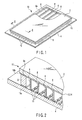
- FIG. 1 is a perspective view of the vacuum envelope 10 of the PED, showing the front substrate partly cut away.
- the envelope 10 may be also called display panel 10.
- FIG. 2 is a sectional view of the vacuum envelope 10 shown in FIG. 1, taken along line II-II.
- FIG. 3 is a magnified sectional view of a part of the envelope shown in FIG. 2.
- the display panel 10 comprises a front substrate 2 and a rear substrate 4, which are rectangular glass plates.
- the substrates 2 and 4 are opposed to each other, arranged parallel to each other and spaced apart by a gap of about 1.0 to 2.0 mm.
- the rear substrate 4 has is larger in sized than the front substrate 2.
- the front substrate 2 and the rear substrate 4 are coupled, at peripheral edges, by a sidewall 6 that is a rectangular frame made of glass. They constitute a vacuum envelope of flat-panel structure, in which a vacuum is maintained.
- a phosphor screen 12 is formed on the inner surface of the front substrate 2.
- the screen 12 functions as image display screen.
- the phosphor screen 12 comprises red phosphor layers R, blue phosphor layers B, green phosphor layers G, and light-shielding layers 11.
- the phosphor layers are provided in the form of stripes or dots.
- a metal-back layer 14 made of aluminum is formed on the phosphor screen 12.
- the electron emission elements 16 are sources of electrons and emit electron beams, which will excite the phosphor layers R, G and B of the phosphor screen 12.
- the electron emission elements 16 are arranged in rows and columns, each provided for one pixel composed of a phosphor layer R, a phosphor layer G and a phosphor layer B.
- Each electron emission element 16 comprises an electron-emitting member 24 (see FIG. 4) and a pair of element electrodes 21 and 22 (see FIG. 4). The member 24 will be described later.
- the element electrodes 21 and 22 are used to apply a voltage to the electron-emitting member.
- a number of wires 18 are arranged in the form of a matrix, to apply a drive voltage to each electron emission element 16. The wires are led, at one end, from the vacuum envelope 10.
- the sidewall 6 that functions as coupling member is bonded to the peripheral edges of the front substrate 2 and the peripheral edges of the rear substrate 4, with sealing material 19 such as lo-melting glass or low-melting metal, thus bonding the substrates to each other.
- the sidewall 6 is bonded to the rear substrate 4 by using frit glass 19a, and is bonded to the front substrate 2 by using indium 19b.
- Low-melting metal may be used to bond the sidewall 6 to the rear substrate 4 on which the wires 18 are provided.
- an insulating layer must be provide as intermediate layer, in order to avoid short circuiting between any wire 18 and the sealing material 19.
- the display panel 10 has a plurality of spacers 8, which are provided between the front substrate 2 and the rear substrate 4.
- the spacers 8 are elongated plates made of glass.
- the spacers 8 are elongated glass plates in this embodiment. Instead, they may be a number of pillar-like spacers (not shown) which are integrally formed with a grid (not shown) that is a rectangular metal plate and which stand on both surfaces of the grid.
- Each spacer 8 has an upper end 8a and a lower end 8b.
- the upper end 8a abuts on the light-shielding layers 11 of the phosphor screen 12, which in turn abuts on the inner surface of the front substrate 2.
- the lower end 8b abuts on the wires 18 provided on the inner surface of the rear substrate 4.
- the PED further comprises a voltage-applying unit (not shown), which applies an anode voltage between the metal-back layer 14 of the front substrate 2 and the rear substrate 4.
- the voltage-applying unit applies an anode voltage between the metal-back layer 14 and the rear substrate 4 so that the potentials of the rear substrate 4 and metal-back layer 14 may be set to, for example, 0V and about 10 kV, respectively.
- a voltage is applied between the element electrodes of any selected electron emission element 16 via a drive circuit (not shown) that is connected to the wires 18, in order to display an image.
- the electron-emitting members of selected electron emission elements emits electron beams.
- an anode voltage is applied to the metal-back layer 14. The anode voltage accelerates the electron beams emitted from the electron emission elements.
- the electron beams are applied to the phosphor screen 12, exciting the phosphor layers R, G and B of the screen 12.
- the phosphor layers emit color light beams. As a result, the PED displays a color image.
- the front substrate 2 is prepared, with the phosphor screen 12 and the metal-back layer 14 already provided on it.
- the rear substrate 4 is prepared, too, with the element emission elements 16 and the wires 18 already provided on it.
- the front substrate 2 and the rear substrate 4 are arranged in the vacuum chamber (not shown). After the vacuum chamber is evacuated, generating a vacuum in it, the front substrate 2 is bonded to the rear substrate 4, with the sidewall 6 interposed between the substrates 2 and 4.
- the display panel 10 having a plurality of spacers 8 is thereby manufactured.
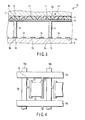
- FIG. 4 is a plan view schematically depicting one of the electron emission elements 16 provided the present embodiment of this invention, as viewed from the inner surface of the rear substrate 4.
- the electron emission element 16 has a pair of element electrodes 21 and 22 and an electron-emitting member 24.
- the electrodes 21 and 22 are connected to wires 18.
- the member 24 connects the element electrodes 21 and 22.
- wires 18, i.e., signal lines 18a and 18b and scanning lines 18c and 18d are arrange on the inner surface 4a of the rear substrate 4.
- the signal lines 18a and 18b are insulated from the scanning lines 18c and 18d, by a barrier-metal layer (not shown).
- the lines 18a, 18b, 18c and 18d are arranged in the form of a matrix.
- One electron emission element 16 is formed at the intersection of one signal line and one scanning line.
- one element electrode 21 is connected to the signal line 18a, the other element electrode 22 is connected to the scanning line 18c.
- a PZT film 24, i.e., electron-emitting member, is provided and connects the paired element electrodes.
- the PZT film 24 is a ferroelectric film, which is thin and made of an oxide containing zinc (Zn) and titanium (Ti).
- the film 24 emits electrons when a predetermined voltage is applied between the element electrodes 21 and 22 that contact this thin film. That is, the PZT film 24 is heated, emitting electrons from its surface, when the predetermined voltage is applied between the paired element electrodes 21 and 22. The electrons are accelerated by the anode voltage and cause the phosphor layers R, G and B to emit light. Electrons may be emitted from the surface of the PZT film 24 by heating the PZT film 24 to a predetermined temperature by means of a heater or the like.
- a device using a PZT film as an electron source is the semiconductor device that is disclosed in Integrated Ferroelectrics, 2001, Vol. 41, pp. 17-25 .
- the reference teaches that BaTiO 3 can be used as an electron source.
- BaTiO 3 can be used in the device according to this invention, in place of the PZT film 24.
- the ferroelectric film 24, e.g., PZT film is rectangular in conformity with the shape of the phosphor layers R, G and B. This is because the shape of the spot of the electron beam emitted from the film 24 is determined by the shape of the film 24. Since the film 24 has almost the same shape as the phosphor layers, electron beams can be efficiently applied to almost all area of each phosphor layer. Nonetheless, the PZT film 24 may have an oblate shape that is similar to the shape of the phosphor layers.
- the shape of the electron beam can be designed to any shape desired. This can increase the emission efficiency of the phosphor layers R, G and B, ultimately enhancing the display luminance and lengthening the lifetime of the phosphor layers. That is, the beam spot can have a desired shaped, preventing the application of the electron beam to only a limited part of each phosphor layer R, G or B. Hence, the lifetime of phosphor layers can be lengthened.
- Step S1 sputtering is performed, coating the inner surface 4a of the rear substrate 4 with platinum and thus forming a barrier-metal layer (Step S1).
- Lower wires i.e., signal lines 18a and 18b, are formed by applying photoresist (Step S2).
- an insulting layer is formed (Step S3).
- Step S5 a pair of element electrodes 21 and 22 are formed.
- a PZT film 24 is formed on an insulating layer and patterned, thus connecting the electrodes 21 and 22 (Step S7).
- a PZT film is formed by sputtering and a resist layer is formed by spin-coating or spray-coating.
- the resist is exposed to light, using a predetermined mask pattern.
- the resist is the peeled off, forming a pattern.
- ink prepared by mixing PZT particles made by crushing, with a binder may be printed and baked, thereby to provide a pattered PZT film 24.
- the electron emission element 16 can be produced in simple steps, reducing the manufacturing cost of the display device.
- electron emission elements can be provided, which do not differ in terms of electron-emitting characteristic.
- the present invention is not limited to the embodiment described above.
- the components of any embodiment can be modified in various manners in reducing the invention to practice, without departing from the sprit or scope of the invention.
- the components of any embodiment described above may be combined, if necessary, in various ways to make different inventions. For example, some of the component of any embodiment may not be used.
- the components of the different embodiments may be combined in any desired fashion.
- the display device is configured and operates, as described above. Therefore, the electron emission elements provided in the device can be easily manufactured at low cost and have stable electron-emitting characteristic, and the electron beams emitted from the electron emission elements can have such a shape as desired.
Landscapes
- Cathode-Ray Tubes And Fluorescent Screens For Display (AREA)
- Devices For Indicating Variable Information By Combining Individual Elements (AREA)
- Electrodes For Cathode-Ray Tubes (AREA)
Abstract
A PED is constituted by arranging signal lines (18a, 18b) and scanning lines (18c, 18d), in the form of a matrix, on the inner surface (4a) of a rear substrate and by forming PZT films (24), which are used as electron-emitting members, at the intersections of the signal lines and the scanning lines. When a voltage is applied between element electrodes (21, 22) connected to the lines, each PZT film (24) emits an electron beam having a cross-section shape that depends on the shape of the PZT film (24).
Description
- The present invention relates to a display device in which the electron emission elements provided on the rear substrate emit electrons and the phosphor layers provided on the front substrate are excited, thereby displaying a color image.
- In recent years, field-emission displays (FEDs), plasma displays (PDPs) and like have been known as displays that have a vacuum envelope of flat-panel structure. Displays having electron emission elements of surface-conduction type (hereinafter referred to as SEDs) are now being developed as one type of FEDs.
- The SED has a front substrate and a rear substrate, which are opposed to each other and spaced apart by a predetermined gap. These substrates are coupled with each other at edges, by a sidewall that is shaped like a rectangular frame. The substrates constitute a vacuum envelope which has a flat panel structure and the interior of which remains in a vacuum.
- Phosphor layers that can emit three-color light beams are formed on the inner surface of the front substrate. On the inner surface of the rear substrate, a number of electron emission elements are arranged and used as sources of electrons, each corresponding to one pixel. On the inner surface of the rear substrate, too, a number of wires are arranged in the form of a matrix, for driving the electron emission elements. These wires are led, at one end, from the vacuum envelope.
- Each electron emission element has a pair of element electrodes and a conductive film. The electrodes are connected to wires. The conductive film connects the element electrodes. A crack is made in the conductive film, between the element electrodes (see, for example, Jpn. Pat. Appln. KOKAI Publication No.
9-237571 - In the process of forming each electron emission element, a high pulse voltage is applied between the element electrodes after the conductive film has been formed, connecting the paired element electrodes. Joule heat is thereby generated, making a crack in the conductive film. To stabilize the width of the crack, i.e., a gap, a pulse voltage is applied between the paired element electrodes in a organic-gas atmosphere, thereby sticking carbon to the edges of the crack.
- As described above, many steps must be performed in order to manufacture the electron emission elements of the conventional SED. This increases the manufacturing cost. In particular, the forming process that makes a crack in the conductive film must be carried out in a vacuum, and the activation process of sticking carbon to the rack must be performed in a predetermined organic-gas atmosphere. Much time is required to prepare these atmospheres. Consequently, it takes a long time to manufacture the SED.
- In manufacturing the conventional SED, Joule heat is applied, making a crack in the conductive film and thereby forming an electron-emitting unit. Hence, even if the activation process is performed to stick carbon, each electron emission element will have a gap different form that in any other element. As a result, the electron emission elements may differ in terms of electron-emitting characteristic.
- In the conventional SED, the electron beam emitted from each electron emission element is elongated. Inevitably, the beam spot is elongated, too. Consequently, each phosphor layer is degraded at a limited part, which inevitably shortens the lifetime of the entire phosphor layer.
- An object of the present invention is to provide a display device which can be easily manufactured at low cost and in which each electron emission element has stable electron-emitting characteristic and can emit an electron beam that can have a shape as desired.
- To achieve this object, a display device according to this invention is characterized by having a vacuum envelope constituted by opposing a front substrate having a plurality of phosphor layers, to a rear substrate having a plurality of electron emission elements corresponding to the phosphor layers, respectively, and wires for driving the electron emission elements, by aligning the front substrate and the rear substrate in position, by bonding the front substrate and the rear substrate to each other at peripheral edges, and by generating a vacuum in the envelope, thus forming an envelope. Each of the electron emission elements has: a pair of element electrodes which are connected to the wires; and an electron-emitting member. The electron-emitting member is made of material that emits electrons when a potential is applied between the element electrodes connected to the electron-emitting member.
- According to the invention, electrons can be emitted only by applying a voltage to the electron-emitting member that connects a pair of electrodes. This helps to simplify the structure of the electron emission element. Further, the shape and characteristic of the electron beam can be changed by changing the shape and thickness of the electron-emitting member. Therefore, an electron beam having a desired characteristic can be emitted.
- Another display device according to the present invention is characterized by having a vacuum envelope constituted by opposing a front substrate having a plurality of phosphor layers, to a rear substrate having a plurality of electron emission elements corresponding to the phosphor layers, respectively, by aligning the front substrate and the rear substrate in position, by bonding the front substrate and the rear substrate to each other at peripheral edges, and by generating a vacuum in the envelope, thus forming an envelope. Each of the electron emission elements has an electron-emitting member which is configured to emit electrons when heated to a predetermined temperature; and a heater which heats the electron-emitting member to the predetermined temperature.
- According to this invention, the heater of each electron-emitting member is operated to emit electrons. This helps to simplify the structure of the electron emission element. Further, the shape and characteristic of the electron beam can be changed by changing the shape and thickness of the electron-emitting member. Therefore, an electron beam having a desired characteristic can be emitted.
-
- FIG. 1 is a perspective view showing the outer appearance of the vacuum envelope of a PED according to an embodiment of the present invention;
- FIG. 2 is a sectional perspective view of the vacuum envelope of FIG. 1, taken along line II-II;
- FIG. 3 is a magnified sectional view of a part of the envelope shown in FIG. 2;
- FIG. 4 is a plan view showing the wiring configuration of an electron emission element of the PED; and
- FIG. 5 is a flowchart explaining a method of manufacturing the electron emission element shown in FIG. 4.
- An embodiment of the present invention will be described, with reference to the accompanying drawings.
- First, a pyroelectric emission display (PED), which is a display device according to this invention, will be described with reference to FIGS. 1 to 3. FIG. 1 is a perspective view of the
vacuum envelope 10 of the PED, showing the front substrate partly cut away. (Hereinafter, theenvelope 10 may be also calleddisplay panel 10.) FIG. 2 is a sectional view of thevacuum envelope 10 shown in FIG. 1, taken along line II-II. FIG. 3 is a magnified sectional view of a part of the envelope shown in FIG. 2. - As shown in FIG. 1 to FIG. 3, the
display panel 10 comprises afront substrate 2 and arear substrate 4, which are rectangular glass plates. Thesubstrates rear substrate 4 has is larger in sized than thefront substrate 2. Thefront substrate 2 and therear substrate 4 are coupled, at peripheral edges, by asidewall 6 that is a rectangular frame made of glass. They constitute a vacuum envelope of flat-panel structure, in which a vacuum is maintained. - A
phosphor screen 12 is formed on the inner surface of thefront substrate 2. Thescreen 12 functions as image display screen. Thephosphor screen 12 comprises red phosphor layers R, blue phosphor layers B, green phosphor layers G, and light-shieldinglayers 11. The phosphor layers are provided in the form of stripes or dots. A metal-back layer 14 made of aluminum is formed on thephosphor screen 12. - On the inner surface of the
rear substrate 4, a number ofelectron emission elements 16 are provided. Theelectron emission elements 16 are sources of electrons and emit electron beams, which will excite the phosphor layers R, G and B of thephosphor screen 12. Theelectron emission elements 16 are arranged in rows and columns, each provided for one pixel composed of a phosphor layer R, a phosphor layer G and a phosphor layer B. Eachelectron emission element 16 comprises an electron-emitting member 24 (see FIG. 4) and a pair ofelement electrodes 21 and 22 (see FIG. 4). Themember 24 will be described later. Theelement electrodes rear substrate 4, a number ofwires 18 are arranged in the form of a matrix, to apply a drive voltage to eachelectron emission element 16. The wires are led, at one end, from thevacuum envelope 10. - The
sidewall 6 that functions as coupling member is bonded to the peripheral edges of thefront substrate 2 and the peripheral edges of therear substrate 4, with sealing material 19 such as lo-melting glass or low-melting metal, thus bonding the substrates to each other. In the present embodiment, thesidewall 6 is bonded to therear substrate 4 by usingfrit glass 19a, and is bonded to thefront substrate 2 by usingindium 19b. Low-melting metal may be used to bond thesidewall 6 to therear substrate 4 on which thewires 18 are provided. In this case, an insulating layer must be provide as intermediate layer, in order to avoid short circuiting between anywire 18 and the sealing material 19. - The
display panel 10 has a plurality ofspacers 8, which are provided between thefront substrate 2 and therear substrate 4. Thespacers 8 are elongated plates made of glass. Thespacers 8 are elongated glass plates in this embodiment. Instead, they may be a number of pillar-like spacers (not shown) which are integrally formed with a grid (not shown) that is a rectangular metal plate and which stand on both surfaces of the grid. - Each
spacer 8 has anupper end 8a and alower end 8b. Theupper end 8a abuts on the light-shieldinglayers 11 of thephosphor screen 12, which in turn abuts on the inner surface of thefront substrate 2. Thelower end 8b abuts on thewires 18 provided on the inner surface of therear substrate 4. Thus, thespacers 8 support thefront substrate 2 and therear substrate 4 against the atmospheric pressure exerted to the outer surface of therear substrate 4, maintaining the gap between the substrates at a predetermined value. - The PED further comprises a voltage-applying unit (not shown), which applies an anode voltage between the metal-
back layer 14 of thefront substrate 2 and therear substrate 4. The voltage-applying unit applies an anode voltage between the metal-back layer 14 and therear substrate 4 so that the potentials of therear substrate 4 and metal-back layer 14 may be set to, for example, 0V and about 10 kV, respectively. - In the PED, a voltage is applied between the element electrodes of any selected
electron emission element 16 via a drive circuit (not shown) that is connected to thewires 18, in order to display an image. The electron-emitting members of selected electron emission elements emits electron beams. Meanwhile, an anode voltage is applied to the metal-back layer 14. The anode voltage accelerates the electron beams emitted from the electron emission elements. The electron beams are applied to thephosphor screen 12, exciting the phosphor layers R, G and B of thescreen 12. The phosphor layers emit color light beams. As a result, the PED displays a color image. - To manufacture the
display panel 10 configured as described above, thefront substrate 2 is prepared, with thephosphor screen 12 and the metal-back layer 14 already provided on it. Therear substrate 4 is prepared, too, with theelement emission elements 16 and thewires 18 already provided on it. Then, thefront substrate 2 and therear substrate 4 are arranged in the vacuum chamber (not shown). After the vacuum chamber is evacuated, generating a vacuum in it, thefront substrate 2 is bonded to therear substrate 4, with thesidewall 6 interposed between thesubstrates display panel 10 having a plurality ofspacers 8 is thereby manufactured. - FIG. 4 is a plan view schematically depicting one of the
electron emission elements 16 provided the present embodiment of this invention, as viewed from the inner surface of therear substrate 4. Theelectron emission element 16 has a pair ofelement electrodes member 24. Theelectrodes wires 18. Themember 24 connects theelement electrodes - More specifically,
wires 18, i.e.,signal lines scanning lines inner surface 4a of therear substrate 4. Thesignal lines scanning lines lines electron emission element 16 is formed at the intersection of one signal line and one scanning line. In the case of FIG. 4, oneelement electrode 21 is connected to thesignal line 18a, theother element electrode 22 is connected to thescanning line 18c. APZT film 24, i.e., electron-emitting member, is provided and connects the paired element electrodes. - The
PZT film 24 is a ferroelectric film, which is thin and made of an oxide containing zinc (Zn) and titanium (Ti). Thefilm 24 emits electrons when a predetermined voltage is applied between theelement electrodes PZT film 24 is heated, emitting electrons from its surface, when the predetermined voltage is applied between the pairedelement electrodes PZT film 24 by heating thePZT film 24 to a predetermined temperature by means of a heater or the like. - Known as a device using a PZT film as an electron source is the semiconductor device that is disclosed in Integrated Ferroelectrics, 2001, Vol. 41, pp. 17-25. The reference teaches that BaTiO3 can be used as an electron source. Hence, BaTiO3 can be used in the device according to this invention, in place of the
PZT film 24. - In the present embodiment, the
ferroelectric film 24, e.g., PZT film, is rectangular in conformity with the shape of the phosphor layers R, G and B. This is because the shape of the spot of the electron beam emitted from thefilm 24 is determined by the shape of thefilm 24. Since thefilm 24 has almost the same shape as the phosphor layers, electron beams can be efficiently applied to almost all area of each phosphor layer. Nonetheless, thePZT film 24 may have an oblate shape that is similar to the shape of the phosphor layers. - In other words, since the
PZT film 24 is used as an electron-emitting member, the shape of the electron beam can be designed to any shape desired. This can increase the emission efficiency of the phosphor layers R, G and B, ultimately enhancing the display luminance and lengthening the lifetime of the phosphor layers. That is, the beam spot can have a desired shaped, preventing the application of the electron beam to only a limited part of each phosphor layer R, G or B. Hence, the lifetime of phosphor layers can be lengthened. - A method of manufacturing each
electron emission elements 16 will be explained, with reference to FIG. 4 and the flowchart of FIG. 5. - First, sputtering is performed, coating the
inner surface 4a of therear substrate 4 with platinum and thus forming a barrier-metal layer (Step S1). Lower wires, i.e.,signal lines lines - Next, a pair of
element electrodes PZT film 24 is formed on an insulating layer and patterned, thus connecting theelectrodes 21 and 22 (Step S7). At this time, a PZT film is formed by sputtering and a resist layer is formed by spin-coating or spray-coating. The resist is exposed to light, using a predetermined mask pattern. The resist is the peeled off, forming a pattern. - Alternatively, ink prepared by mixing PZT particles made by crushing, with a binder, may be printed and baked, thereby to provide a pattered
PZT film 24. - Thus, the
electron emission element 16 can be produced in simple steps, reducing the manufacturing cost of the display device. To manufacture eachelectron emission element 16, it is not necessary to make a crack in the forming process and stick carbon to the crack as in the method of manufacturing the electron emission elements of, for example, an SED, after forming the conductive film that connects the element electrodes. Hence, electron emission elements can be provided, which do not differ in terms of electron-emitting characteristic. - The present invention is not limited to the embodiment described above. The components of any embodiment can be modified in various manners in reducing the invention to practice, without departing from the sprit or scope of the invention. Further, the components of any embodiment described above may be combined, if necessary, in various ways to make different inventions. For example, some of the component of any embodiment may not be used. Moreover, the components of the different embodiments may be combined in any desired fashion.
- The display device according to the present invention is configured and operates, as described above. Therefore, the electron emission elements provided in the device can be easily manufactured at low cost and have stable electron-emitting characteristic, and the electron beams emitted from the electron emission elements can have such a shape as desired.
Claims (10)
- A display device characterized by having a vacuum envelope constituted by opposing a front substrate having a plurality of phosphor layers, to a rear substrate having a plurality of electron emission elements corresponding to the phosphor layers, respectively, and wires for driving the electron emission elements, by aligning the front substrate and the rear substrate in position, by bonding the front substrate and the rear substrate to each other at peripheral edges, and by generating a vacuum in the envelope, thus forming an envelope,
each of the electron emission elements having:a pair of element electrodes which are connected to the wires; andan electron-emitting member which is provided, connecting the paired element electrodes,the electron-emitting member being made of material that emits electrons when a potential is applied between the element electrodes connected to the electron-emitting member. - The display device according to claim 1, characterized in that the electron-emitting member is constituted by a ferroelectric film such as PZT film.
- The display device according to claim 2, characterized in that the ferroelectric film is substantially rectangular in conformity with a shape of the phosphor layers.
- The display device according to claim 2, characterized in that the ferroelectric film is oblate.
- The display device according to claim 1, characterized in that the electron-emitting member is made of BaTiO3.
- A display device characterized by having a vacuum envelope constituted by opposing a front substrate having a plurality of phosphor layers, to a rear substrate having a plurality of electron emission elements corresponding to the phosphor layers, respectively, by aligning the front substrate and the rear substrate in position, by bonding the front substrate and the rear substrate to each other at peripheral edges, and by generating a vacuum in the envelope, thus forming an envelope,
each of the electron emission elements having:an electron-emitting member which is configured to emit electrons when heated to a predetermined temperature; anda heater which heats the electron-emitting member to the predetermined temperature. - The display device according to claim 6, characterized in that the electron-emitting member is constituted by a ferroelectric film such as PZT film.
- The display device according to claim 7, characterized in that the ferroelectric film is substantially rectangular in conformity with a shape of the phosphor layers.
- The display device according to claim 7, characterized in that the ferroelectric film is oblate.
- The display device according to claim 6, characterized in that the electron-emitting member is made of BaTiO3.
Applications Claiming Priority (2)
| Application Number | Priority Date | Filing Date | Title |
|---|---|---|---|
| JP2004250202A JP2006066336A (en) | 2004-08-30 | 2004-08-30 | Display device |
| PCT/JP2005/014105 WO2006025175A1 (en) | 2004-08-30 | 2005-08-02 | Display unit |
Publications (1)
| Publication Number | Publication Date |
|---|---|
| EP1786016A1 true EP1786016A1 (en) | 2007-05-16 |
Family
ID=35999836
Family Applications (1)
| Application Number | Title | Priority Date | Filing Date |
|---|---|---|---|
| EP05768629A Withdrawn EP1786016A1 (en) | 2004-08-30 | 2005-08-02 | Display unit |
Country Status (7)
| Country | Link |
|---|---|
| US (1) | US20070126338A1 (en) |
| EP (1) | EP1786016A1 (en) |
| JP (1) | JP2006066336A (en) |
| KR (1) | KR20070039163A (en) |
| CN (1) | CN101006544A (en) |
| TW (1) | TW200609973A (en) |
| WO (1) | WO2006025175A1 (en) |
Families Citing this family (1)
| Publication number | Priority date | Publication date | Assignee | Title |
|---|---|---|---|---|
| JP2008052135A (en) * | 2006-08-25 | 2008-03-06 | Canon Inc | Image display device and manufacturing method thereof |
Family Cites Families (8)
| Publication number | Priority date | Publication date | Assignee | Title |
|---|---|---|---|---|
| KR0170221B1 (en) * | 1989-12-30 | 1999-02-01 | 김정배 | Dispenser cathode |
| JPH04289628A (en) * | 1991-03-19 | 1992-10-14 | Canon Inc | Electron emission element and manufacture thereof, and electron beam generator and picture display using the element |
| JPH0872292A (en) * | 1994-09-09 | 1996-03-19 | Alps Electric Co Ltd | Ion write head |
| JPH1048042A (en) * | 1996-08-05 | 1998-02-20 | Osaka Gas Co Ltd | Pyroelectric type infrared ray sensor |
| JPH10116576A (en) * | 1996-10-09 | 1998-05-06 | Dainippon Printing Co Ltd | Electron emission device for image display |
| JPH11185600A (en) * | 1997-12-22 | 1999-07-09 | Minolta Co Ltd | Electron emitting device and image forming device |
| JP4114264B2 (en) * | 1999-03-16 | 2008-07-09 | 株式会社村田製作所 | Ferroelectric electron emission cold cathode |
| JP2001312958A (en) * | 2000-04-28 | 2001-11-09 | Canon Inc | Electron source and image forming apparatus |
-
2004
- 2004-08-30 JP JP2004250202A patent/JP2006066336A/en active Pending
-
2005
- 2005-08-02 EP EP05768629A patent/EP1786016A1/en not_active Withdrawn
- 2005-08-02 CN CNA2005800284746A patent/CN101006544A/en active Pending
- 2005-08-02 WO PCT/JP2005/014105 patent/WO2006025175A1/en not_active Ceased
- 2005-08-02 KR KR1020077004612A patent/KR20070039163A/en not_active Ceased
- 2005-08-16 TW TW094127795A patent/TW200609973A/en unknown
-
2007
- 2007-02-05 US US11/671,302 patent/US20070126338A1/en not_active Abandoned
Non-Patent Citations (1)
| Title |
|---|
| See references of WO2006025175A1 * |
Also Published As
| Publication number | Publication date |
|---|---|
| JP2006066336A (en) | 2006-03-09 |
| CN101006544A (en) | 2007-07-25 |
| TW200609973A (en) | 2006-03-16 |
| US20070126338A1 (en) | 2007-06-07 |
| WO2006025175A1 (en) | 2006-03-09 |
| KR20070039163A (en) | 2007-04-11 |
Similar Documents
| Publication | Publication Date | Title |
|---|---|---|
| JP3619085B2 (en) | Image forming apparatus, manufacturing method thereof, and storage medium | |
| CN1518048B (en) | field emission display | |
| KR100357005B1 (en) | Image forming apparatus for forming image by electron irradiation | |
| KR100709173B1 (en) | Image display apparatus and method for manufacturing the same | |
| TW583707B (en) | Flat-panel display and flat-panel display cathode manufacturing method | |
| JP5150156B2 (en) | Driving method of flat display device | |
| US20070126338A1 (en) | Display device | |
| TWI281686B (en) | Image display device | |
| EP1833074B1 (en) | Image display device | |
| JP2006173007A (en) | ELECTRON EMITTING ELEMENT, ELECTRON EMITTING DEVICE, AND DISPLAY DEVICE | |
| JP2002203475A (en) | Electron source substrate, method of manufacturing electron source substrate, and image display device including electron source substrate | |
| JP3938185B2 (en) | Image display device and manufacturing method thereof | |
| EP1760757A1 (en) | Image display device and method for manufacturing the same | |
| WO2001026128A1 (en) | Electron source, method of manufacture thereof, and display device | |
| JP2000260358A (en) | Image display device | |
| EP1814135A1 (en) | Image display device and method for manufacturing the same | |
| WO2005020271A1 (en) | Image display device | |
| WO2005096398A1 (en) | Image display | |
| JP2006107739A (en) | Manufacturing method of image display device | |
| JP2005259517A (en) | Display device | |
| JP2006066201A (en) | Image display device and manufacturing method thereof | |
| WO2007017990A1 (en) | Display | |
| JP2006073314A (en) | Manufacturing method of display device | |
| JPH08138583A (en) | Image display device | |
| JPH07226176A (en) | Flat display device |
Legal Events
| Date | Code | Title | Description |
|---|---|---|---|
| PUAI | Public reference made under article 153(3) epc to a published international application that has entered the european phase |
Free format text: ORIGINAL CODE: 0009012 |
|
| 17P | Request for examination filed |
Effective date: 20070205 |
|
| AK | Designated contracting states |
Kind code of ref document: A1 Designated state(s): DE FR GB IT NL |
|
| DAX | Request for extension of the european patent (deleted) | ||
| RBV | Designated contracting states (corrected) |
Designated state(s): DE FR GB IT NL |
|
| STAA | Information on the status of an ep patent application or granted ep patent |
Free format text: STATUS: THE APPLICATION HAS BEEN WITHDRAWN |
|
| 18W | Application withdrawn |
Effective date: 20080226 |