EP1785770A2 - Stamp for micro/nano imprint lithography using diamond-like carbon and method of fabricating the same - Google Patents
Stamp for micro/nano imprint lithography using diamond-like carbon and method of fabricating the same Download PDFInfo
- Publication number
- EP1785770A2 EP1785770A2 EP06021860A EP06021860A EP1785770A2 EP 1785770 A2 EP1785770 A2 EP 1785770A2 EP 06021860 A EP06021860 A EP 06021860A EP 06021860 A EP06021860 A EP 06021860A EP 1785770 A2 EP1785770 A2 EP 1785770A2
- Authority
- EP
- European Patent Office
- Prior art keywords
- thin film
- diamond
- micro
- stamp
- imprint lithography
- Prior art date
- Legal status (The legal status is an assumption and is not a legal conclusion. Google has not performed a legal analysis and makes no representation as to the accuracy of the status listed.)
- Granted
Links
Images



Classifications
-
- G—PHYSICS
- G03—PHOTOGRAPHY; CINEMATOGRAPHY; ANALOGOUS TECHNIQUES USING WAVES OTHER THAN OPTICAL WAVES; ELECTROGRAPHY; HOLOGRAPHY
- G03F—PHOTOMECHANICAL PRODUCTION OF TEXTURED OR PATTERNED SURFACES, e.g. FOR PRINTING, FOR PROCESSING OF SEMICONDUCTOR DEVICES; MATERIALS THEREFOR; ORIGINALS THEREFOR; APPARATUS SPECIALLY ADAPTED THEREFOR
- G03F7/00—Photomechanical, e.g. photolithographic, production of textured or patterned surfaces, e.g. printing surfaces; Materials therefor, e.g. comprising photoresists; Apparatus specially adapted therefor
- G03F7/0002—Lithographic processes using patterning methods other than those involving the exposure to radiation, e.g. by stamping
-
- B—PERFORMING OPERATIONS; TRANSPORTING
- B41—PRINTING; LINING MACHINES; TYPEWRITERS; STAMPS
- B41K—STAMPS; STAMPING OR NUMBERING APPARATUS OR DEVICES
- B41K3/00—Apparatus for stamping articles having integral means for supporting the articles to be stamped
-
- B—PERFORMING OPERATIONS; TRANSPORTING
- B81—MICROSTRUCTURAL TECHNOLOGY
- B81C—PROCESSES OR APPARATUS SPECIALLY ADAPTED FOR THE MANUFACTURE OR TREATMENT OF MICROSTRUCTURAL DEVICES OR SYSTEMS
- B81C1/00—Manufacture or treatment of devices or systems in or on a substrate
- B81C1/00436—Shaping materials, i.e. techniques for structuring the substrate or the layers on the substrate
- B81C1/00444—Surface micromachining, i.e. structuring layers on the substrate
- B81C1/0046—Surface micromachining, i.e. structuring layers on the substrate using stamping, e.g. imprinting
-
- B—PERFORMING OPERATIONS; TRANSPORTING
- B82—NANOTECHNOLOGY
- B82Y—SPECIFIC USES OR APPLICATIONS OF NANOSTRUCTURES; MEASUREMENT OR ANALYSIS OF NANOSTRUCTURES; MANUFACTURE OR TREATMENT OF NANOSTRUCTURES
- B82Y10/00—Nanotechnology for information processing, storage or transmission, e.g. quantum computing or single electron logic
-
- B—PERFORMING OPERATIONS; TRANSPORTING
- B82—NANOTECHNOLOGY
- B82Y—SPECIFIC USES OR APPLICATIONS OF NANOSTRUCTURES; MEASUREMENT OR ANALYSIS OF NANOSTRUCTURES; MANUFACTURE OR TREATMENT OF NANOSTRUCTURES
- B82Y40/00—Manufacture or treatment of nanostructures
-
- H—ELECTRICITY
- H10—SEMICONDUCTOR DEVICES; ELECTRIC SOLID-STATE DEVICES NOT OTHERWISE PROVIDED FOR
- H10P—GENERIC PROCESSES OR APPARATUS FOR THE MANUFACTURE OR TREATMENT OF DEVICES COVERED BY CLASS H10
- H10P14/00—Formation of materials, e.g. in the shape of layers or pillars
- H10P14/20—Formation of materials, e.g. in the shape of layers or pillars of semiconductor materials
- H10P14/34—Deposited materials, e.g. layers
- H10P14/3402—Deposited materials, e.g. layers characterised by the chemical composition
- H10P14/3404—Deposited materials, e.g. layers characterised by the chemical composition being Group IVA materials
- H10P14/3406—Carbon, e.g. diamond-like carbon
-
- Y—GENERAL TAGGING OF NEW TECHNOLOGICAL DEVELOPMENTS; GENERAL TAGGING OF CROSS-SECTIONAL TECHNOLOGIES SPANNING OVER SEVERAL SECTIONS OF THE IPC; TECHNICAL SUBJECTS COVERED BY FORMER USPC CROSS-REFERENCE ART COLLECTIONS [XRACs] AND DIGESTS
- Y10—TECHNICAL SUBJECTS COVERED BY FORMER USPC
- Y10S—TECHNICAL SUBJECTS COVERED BY FORMER USPC CROSS-REFERENCE ART COLLECTIONS [XRACs] AND DIGESTS
- Y10S977/00—Nanotechnology
- Y10S977/84—Manufacture, treatment, or detection of nanostructure
- Y10S977/887—Nanoimprint lithography, i.e. nanostamp
Definitions
- the present invention relates to a micro/nano imprint lithography technique and in particular, to a stamp that is used in an UV-micro/nanoimprint lithography process or thermal micro/nano imprint lithography process and a method for fabricating the stamp.
- Micro/nano imprint lithography is a technique to fabricate micro/nano-structures effectively and economically and uses a stamp with embossed micro/nano-structure thereon in a manner that the stamp is pressed on the surface of resist applied on a substrate for imprinting the micro/nano-structure repeatedly.
- a reversed structure to the structure embossed on the stamp is imprinted on the resist of the substrate, and the residual resist in the pressed area is removed by anisotropic etching.
- LADI Laser-Assisted Direct Imprint
- LA-NIL Nanosecond laser-assisted nanoimprint lithography
- Step & Flash Imprint Lithography (SFIL), proposed by professor Sreenivasan et al., is a technique to solve the problems of such a thermal imprint technique.
- the SFIL technique features an ultraviolet (UV) ray-curable material for the resist that enables the fabrication of micro/nano-structures in room temperature and low pressure. It also features an UV ray-transparent material for the stamp substrate such as quartz and Pyrex glass.
- UV ultraviolet
- a transfer layer is firstly coated on a silicon substrate. Then UV ray-curable resin with low viscosity flows in so as to fill the micro-structure of the stamp by surface-tension while the UV ray-transparent stamp is kept from the transfer layer with a predetermined gap. At the time the filling completes, the stamp gets contacted with the transfer layer, and UV-ray is applied in order to cure the resin. Then the stamp is separated, and a micro-structure is imprinted finally on the substrate though etching and lift-off processes.
- Another feature of the SFIL process is the adoption of multiple imprinting by a small unit-sized stamp instead of one imprinting on the entire substrate in a step and repeat way.
- the stamp for the previous microimprint lithography has an anti-sticking layer formed on the stamping surface thereof to prevent the stamp from being stuck with the resist.
- the anti-sticking layer may distort the shape of the pattern embossed on the surface by the thickness of the anti-sticking layer so that the unwanted pattern may be obtained. Also, the structural stability of the anti-sticking layer may be deteriorated when the thickness thereof is reduced.
- the present invention provides a stamp for micro/nano imprint lithography, the stamp including a diamond-like carbon thin film that is hydrophobic and light-transmittable.
- the present invention provides a method for fabricating a stamp for micro/nano imprint lithography, the method in which a diamond-like carbon thin film is deposited on the substrate to form a micro/nano-structure.
- the method for fabricating a stamp for micro/nano imprint lithography includes i) depositing a thin film of diamond-like carbon on a substrate, ii) applying resist on the diamond-like carbon thin film, iii) patterning the resist, iv) etching the diamond-like carbon thin film by using the resist as a protective layer, and v) removing the resist.
- the substrate may be made of a light-transmittable material that may be one of, for example, quartz, glass, diamond, a transparent polymer and a transparent semiconductor such as indium tin oxide (ITO).
- the substrate for thermal imprint may be made of one of an opaque wafer, a semiconductor compound, a polymer, a ceramic material and materials above-mentioned.
- the deposition may be carried out by a process selected from ion plating, plasma chemical vapor deposition (CVD) using direct current (DC) or radio frequency (RF), sputtering using DC, RF or ion-beam, and laser synthesis.
- CVD plasma chemical vapor deposition
- DC direct current
- RF radio frequency
- a gas containing a fluoro group (F) may be poured or the diamond-like carbon thin film is deposited on the sputtered solid substrate containing a fluoro group (F) so as to make the diamond-like carbon thin film include the fluoro group (F).
- At least one of octafluorocyclobutane (C 4 F 8 ), hexafluoroethane (C 2 F 6 ), tetrafluoromethane (CF 4 ), trifluoromethane (CHF 3 ), sulfur hexafluoride (SF 6 ) may be poured as the gas including a fluoro group (F), and fluorocarbon resins may be used as the solid substrate.
- the diamond-like carbon thin film may be etched by plasma etching process including reactive ion etching (RIE).
- plasma etching process including reactive ion etching (RIE).
- the method for fabricating a stamp for micro/nano imprint lithography includes i) depositing a first thin film of diamond-like carbon on a substrate, ii) applying resist on the first diamond-like carbon thin film, iii) patterning the resist, iv) depositing a second diamond-like carbon thin film on top of the patterned resist and on the first diamond-like carbon thin film exposed through openings of the patterned resist, and v) removing the resist.
- a gas containing a fluoro group (F) may be poured or the first diamond-like carbon thin film is deposited on the sputtered solid substrate containing a fluoro group (F) so as to make the first diamond-like carbon thin film or the second diamond-like carbon thin film include the fluoro group (F).
- both of the resist and the second diamond-like carbon thin film deposited on the resist are removed together.
- the method for fabricating a stamp for micro/nano imprint lithography includes i) depositing a first thin film of diamond-like carbon on a substrate, ii) forming micro/nano-structures on top of the first diamond-like carbon thin film, and iii) depositing a second diamond-like carbon thin film to encompass the micro/nano-structures.
- the micro/nano-structures may be made of a resin material.
- a stamp for micro/nano imprint lithography includes a substrate and a micro/nano-structure made of diamond-like carbon thin film on top of the substrate.
- the micro/nano-structure made of diamond-like carbon thin film may include a fluoro group (F).
- a first diamond-like carbon thin film is formed on the substrate, and the micro/nano-structure may be formed by a second diamond-like carbon thin film patterned on top of the first diamond-like carbon thin film.
- micro/nano-structure may be formed by coating the structure made of a resin material with diamond-like carbon thin film.
- the stamp is fabricated by patterning the diamond-like carbon thin film deposited on the substrate, the diamond-like carbon thin film which is hydrophobic and light-transmittable, especially ultraviolet ray-transmittable so that the sticking may be prevented at imprinting between the resist and the stamp without an anti-sticking layer.
- the problems caused by the previous anti-sticking layer may be prevented so that a wanted pattern may be obtained and the process stability may be acquired.
- the hydrophobic property may be improved by pouring a fluorine (F) gas at the deposition of the diamond-like carbon thin film or by sputtering the solid substrate containing a fluoro group (F) so as to include a fluoro group (F).
- F fluorine
- a thin film 15 of diamond-like carbon (DLC) is firstly deposited on a substrate 10 (S11).
- the deposition of the DLC thin film 15 may be carried out by a process selected from ion plating, plasma chemical vapor deposition (CVD) using direct current (DC) or radio frequency (RF), sputtering using DC, RF or ion-beam, and laser synthesis.
- CVD plasma chemical vapor deposition
- DC direct current
- RF radio frequency
- the substrate 10 may be made of a light-transmittable material that may be one of, for example, quartz, glass, diamond, a transparent polymer and a transparent semiconductor such as indium tin oxide (ITO).
- a transparent semiconductor such as indium tin oxide (ITO).
- ITO indium tin oxide
- the substrate 10 partly composing the stamp is preferably made of a light-transmittable material in order to transmit ultraviolet ray through the stamp.
- the substrate 10 for thermal imprint may be made of one of an opaque wafer, a semiconductor compound, a polymer, a ceramic material and materials above-mentioned.
- the DLC film is one of non-crystalline solid-phase carbon films that are as excellent as diamond in hardness, wear resistance, lubrication, electrical insulation, chemical stability and optical property.
- the DLC film is good in hydrophobic property and is capable of light-transmittance, especially UV ray- transmittance.
- the hardness of the DLC film varies widely according to the synthesizing condition and is on the whole as high as silicon carbide (SiC) or aluminum oxide (Al 2 O 3 ).
- the DLC film has a very low friction coefficient.
- the friction coefficient of the DLC film measured by a scratch tester using a diamond tip varies in the range of 0.04 to 0.06, which is lower by about 30 % than that of glass.
- the friction coefficient between diamond and the film or the film and the film is not dependent on humidity.
- the friction coefficient between the steel ball and the film is strongly dependent on humidity.
- the friction coefficient decreases to a value as low as 0.00 to 0.02 as humidity decreases.
- the DLC film has so excellent in chemical stability that it does not react with the most of acid or organic solvent, and no damage is found on the coating even in 80 % aqua regia.
- the most eminent electrical property of the DLC film is a high resistivity.
- the resistivity is in the wide range of 10 4 to 10 14 ohms ( ⁇ ) according to the synthesizing condition.
- a fluorine (F) gas may be added or a fluoro group (F) may be included by sputtering the solid substrate containing a fluoro group (F) in order to improve the hydrophobic property of the DLC thin film 15.
- fluoro group (F) such as octafluorocyclobutane (C 4 F 8 ), hexafluoroethane (C 2 F 6 ), tetrafluoromethane (CF 4 ), trifluoromethane (CHF 3 ), sulfur hexafluoride (SF 6 )
- fluorocarbon resins for example Teflon polytetrafluoroethylene (PTFE) may be used as the solid substrate for a target.
- a resist 18 is applied on top of the DLC thin film 15 (S12). Photoresist may be used as the resist 18.
- Electron-beam lithography or ion-beam lithography may be used for patterning the resist 18.
- the electron-beam lithography process first the electron-beam scans along a wanted pattern on the photoresist that shows chemical changes by the exposure to the electron-beam. Secondly, the patterning of the resist 18 is carried out through developing by removing or leaving the exposed area selectively.
- the resist 18 may be patterned by the ion-beam instead of the electron beam in a similar way to the electron-beam lithography process
- the DLC thin film 15 is etched by using the patterned resist 18 as a protective layer (S14).
- the plasma etching process including reactive ion etching (RIE) is used for etching the DLC thin film 15.
- RIE reactive ion etching
- an etch-resistant etching mask is used, and an anisotropic etching is carried out by using a gas with high selectivity ratio.
- plasma is formed in the area of the DLC thin film 15 to be removed, and electric potential formed outside starts sputtering. Discharge inside the plasma produces chemical reactant from a gas poured in.
- Selected as the etching gas may be a gas that is capable of producing a volatile by-product by reacting with the diamond-like carbon to be removed.
- the stamp for micro/nano imprint lithography of the present embodiment is finished by removing the resist 18 covering the patterned DLC thin film 15. Therefore, the micro/nano-structure of the stamp is made of the DLC thin film 15.
- the stamp made as above may be used for thermal micro/nano imprint lithography as well as UV micro/nano imprint lithography.
- Fig. 3 is a sequential diagram showing processes for fabricating a stamp for micro/nano imprint lithography according to a second embodiment of the present invention
- Figs. 4A to 4D are process diagrams for fabricating a stamp for micro/nano imprint lithography according to the second embodiment of the present invention.
- a first thin film 25 of diamond-like carbon (DLC) is firstly deposited on a substrate 10 (S21).
- the deposition of the DLC thin film 25 may be carried out by one process selected from ion plating, plasma chemical vapor deposition (CVD) using direct current (DC) or radio frequency (RF), sputtering using DC, RF or ion-beam, and laser synthesis.
- CVD plasma chemical vapor deposition
- DC direct current
- RF radio frequency
- the substrate 10 may be made of a light-transmittable material that may be one of, for example, quartz, glass, diamond, a transparent polymer and a transparent semiconductor such as indium tin oxide (ITO).
- a transparent semiconductor such as indium tin oxide (ITO).
- ITO indium tin oxide
- the substrate 10 partly composing the stamp is preferably made of a light-transmittable material in order to transmit ultraviolet ray through the stamp.
- the substrate 10 for thermal imprint may be made of one of an opaque wafer, a semiconductor compound, a polymer, a ceramic material and materials above-mentioned.
- the first DLC thin film 25 may be a material having the same properties as the DLC thin film used in the first embodiment.
- a fluorine (F) gas may be added or a fluoro group (F) may be included by sputtering the solid substrate containing a fluoro group (F).
- a resist 28 is applied on top of the first DLC thin film 25 (S22). Photoresist may be used as the resist 28.
- Electron-beam lithography or ion-beam lithography may be used for patterning the resist 28.
- a second DLC thin film 29 is deposited on top of the patterned resist 28 and on the first DLC thin film 25 exposed through openings of the patterned resist 28 (S24).
- the openings and the cover parts are formed by patterning the resist 28.
- the cover part of the resist 28 serves to cover and hide the first DLC thin film 25, and the opening of the resist 28 serves to expose the first DLC thin film 25.
- the second DLC thin film 29 is deposited on top of the first DLC thin film 25 exposed through openings as well as on top of the cover parts of the resist 28.
- a fluorine (F) gas may be added or a fluoro group (F) may be included by sputtering the solid substrate containing a fluoro group (F).
- the second DLC thin film 29b deposited on the resist 28 is removed together. Therefore, only the second DLC thin film 29a deposited on the first DLC thin film 25 remains so as to form the micro/nano-structure after the resist 28 is removed. That is the finished stamp of the micro/nano imprint lithography of the present embodiment.
- the stamp made as above may be used for thermal micro/nano imprint lithography as well as UV micro/nano imprint lithography.
- Fig. 5 is a sequential diagram showing processes for fabricating a stamp for micro/nano imprint lithography according to a third embodiment of the present invention
- Figs. 6A to 6D are process diagrams for fabricating a stamp for micro/nano imprint lithography according to the third embodiment of the present invention.
- a first thin film 35 of diamond-like carbon (DLC) is firstly deposited on a substrate 10 (S31).
- the deposition of the DLC thin film 35 may be carried out by one process selected from ion plating, plasma chemical vapor deposition (CVD) using direct current (DC) or radio frequency (RF), sputtering using DC, RF or ion-beam, and laser synthesis.
- CVD plasma chemical vapor deposition
- DC direct current
- RF radio frequency
- the substrate 10 may be made of a light-transmittable material that may be one of, for example, quartz, glass, diamond, a transparent polymer and a transparent semiconductor such as indium tin oxide (ITO).
- a transparent semiconductor such as indium tin oxide (ITO).
- ITO indium tin oxide
- the substrate 10 partly composing the stamp is preferably made of a light-transmittable material in order to transmit ultraviolet ray through the stamp.
- the substrate 10 for thermal imprint may be made of one of an opaque wafer, a semiconductor compound, a polymer, a ceramic material and materials above-mentioned.
- the first DLC thin film 35 may be a material having the same properties as the DLC thin film used in the first embodiment.
- a fluorine (F) gas may be added or a fluoro group (F) may be included by sputtering the solid substrate containing a fluoro group (F).
- micro/nano-structures 37 are formed on the first DLC thin film 35 (S32).
- the micro/nano-structures 37 may be made of a resin material.
- a second DLC thin film 39 is deposited to encompass the micro/nano-structures 37 (S33).
- a fluorine (F) gas may be added or a fluoro group (F) may be included by sputtering the solid substrate containing a fluoro group (F) in order to improve the hydrophobic property of the second DLC thin film 39,
- the stamp for micro/nano imprint lithography of the present embodiment is finished by coating the micro/nano-structures 37 with the second DLC thin film 39.
- the stamp made as above may be applied for thermal micro/nano imprint lithography as well as UV micro/nano imprint lithography.
Landscapes
- Engineering & Computer Science (AREA)
- Nanotechnology (AREA)
- Chemical & Material Sciences (AREA)
- Physics & Mathematics (AREA)
- General Physics & Mathematics (AREA)
- Crystallography & Structural Chemistry (AREA)
- Manufacturing & Machinery (AREA)
- Condensed Matter Physics & Semiconductors (AREA)
- Mathematical Physics (AREA)
- Theoretical Computer Science (AREA)
- Microelectronics & Electronic Packaging (AREA)
- Shaping Of Tube Ends By Bending Or Straightening (AREA)
- Exposure Of Semiconductors, Excluding Electron Or Ion Beam Exposure (AREA)
- Moulds For Moulding Plastics Or The Like (AREA)
Abstract
Description
- The present invention relates to a micro/nano imprint lithography technique and in particular, to a stamp that is used in an UV-micro/nanoimprint lithography process or thermal micro/nano imprint lithography process and a method for fabricating the stamp.
- Micro/nano imprint lithography is a technique to fabricate micro/nano-structures effectively and economically and uses a stamp with embossed micro/nano-structure thereon in a manner that the stamp is pressed on the surface of resist applied on a substrate for imprinting the micro/nano-structure repeatedly.
- Professor Chou suggested the previous microimprint lithography technique in which a stamp with embossed structures in microscale is fabricated first by electron-beam lithography, followed by being contacted with the surface of a resist made of polymethylmethacrylate (PMMA) applied on a substrate, and the stamp is pressed in high temperature and separated off from the substrate after cool-down.
- In the method aforementioned, a reversed structure to the structure embossed on the stamp is imprinted on the resist of the substrate, and the residual resist in the pressed area is removed by anisotropic etching.
- Another imprint lithography technique is Laser-Assisted Direct Imprint (LADI) in which the imprint is carried out by a single 20 ns excimer laser with a wavelength of 308 nm making a resist coated on a silicon wafer (substrate) melted down instantly.
- Another imprint lithography technique is Nanosecond laser-assisted nanoimprint lithography (LA-NIL) in which a polymer material is used as a resist, and micro-structures with 100 nm in line-width and 90 nm in depth may be imprinted thereon.
- All of the imprint techniques aforementioned use heat to cure the resist.
- However, such an imprint technique using heat has difficulty in multiple alignment due to the thermal deformation of the resist when applied for semiconductor fabrication where a multi-layer process is essential. Also, pressure as high as about 30 atms applied to the stamp for imprinting the high viscous resist may cause the break down of the structure made of a heat curable material. Furthermore, the opaqueness of the material used for the stamp substrate causes difficulty in multi-alignment during the process for fabricating the micro-structures.
- Step & Flash Imprint Lithography (SFIL), proposed by professor Sreenivasan et al., is a technique to solve the problems of such a thermal imprint technique.
- The SFIL technique features an ultraviolet (UV) ray-curable material for the resist that enables the fabrication of micro/nano-structures in room temperature and low pressure. It also features an UV ray-transparent material for the stamp substrate such as quartz and Pyrex glass.
- In the SFIL processes, a transfer layer is firstly coated on a silicon substrate. Then UV ray-curable resin with low viscosity flows in so as to fill the micro-structure of the stamp by surface-tension while the UV ray-transparent stamp is kept from the transfer layer with a predetermined gap. At the time the filling completes, the stamp gets contacted with the transfer layer, and UV-ray is applied in order to cure the resin. Then the stamp is separated, and a micro-structure is imprinted finally on the substrate though etching and lift-off processes.
- Recent studies are carried out on the way to press by the stamp the UV ray-curable resin drop placed between the transfer layer and the stamp in the SFIL process.
- Another feature of the SFIL process is the adoption of multiple imprinting by a small unit-sized stamp instead of one imprinting on the entire substrate in a step and repeat way.
- Though this method is efficient to fill the micro-structure due to the small stamping area, it is a shortcoming to take a long time for a substrate with a large base area to be imprinted because each stamping should go through its alignment and imprint.
- On the other hand, the stamp for the previous microimprint lithography has an anti-sticking layer formed on the stamping surface thereof to prevent the stamp from being stuck with the resist.
- However, in the case that the anti-sticking layer is formed on top of the micro/nano-structure smaller in dimension than 50 nm, the anti-sticking layer may distort the shape of the pattern embossed on the surface by the thickness of the anti-sticking layer so that the unwanted pattern may be obtained. Also, the structural stability of the anti-sticking layer may be deteriorated when the thickness thereof is reduced.
- The present invention provides a stamp for micro/nano imprint lithography, the stamp including a diamond-like carbon thin film that is hydrophobic and light-transmittable.
- Also, the present invention provides a method for fabricating a stamp for micro/nano imprint lithography, the method in which a diamond-like carbon thin film is deposited on the substrate to form a micro/nano-structure.
- According to an embodiment of the present invention, the method for fabricating a stamp for micro/nano imprint lithography includes i) depositing a thin film of diamond-like carbon on a substrate, ii) applying resist on the diamond-like carbon thin film, iii) patterning the resist, iv) etching the diamond-like carbon thin film by using the resist as a protective layer, and v) removing the resist.
- The substrate may be made of a light-transmittable material that may be one of, for example, quartz, glass, diamond, a transparent polymer and a transparent semiconductor such as indium tin oxide (ITO). The substrate for thermal imprint may be made of one of an opaque wafer, a semiconductor compound, a polymer, a ceramic material and materials above-mentioned.
- In depositing the diamond-like carbon thin film, the deposition may be carried out by a process selected from ion plating, plasma chemical vapor deposition (CVD) using direct current (DC) or radio frequency (RF), sputtering using DC, RF or ion-beam, and laser synthesis.
- Also, in depositing the diamond-like carbon thin film, a gas containing a fluoro group (F) may be poured or the diamond-like carbon thin film is deposited on the sputtered solid substrate containing a fluoro group (F) so as to make the diamond-like carbon thin film include the fluoro group (F). At least one of octafluorocyclobutane (C4F8), hexafluoroethane (C2F6), tetrafluoromethane (CF4), trifluoromethane (CHF3), sulfur hexafluoride (SF6) may be poured as the gas including a fluoro group (F), and fluorocarbon resins may be used as the solid substrate.
- The diamond-like carbon thin film may be etched by plasma etching process including reactive ion etching (RIE).
- According to another embodiment of the present invention, the method for fabricating a stamp for micro/nano imprint lithography includes i) depositing a first thin film of diamond-like carbon on a substrate, ii) applying resist on the first diamond-like carbon thin film, iii) patterning the resist, iv) depositing a second diamond-like carbon thin film on top of the patterned resist and on the first diamond-like carbon thin film exposed through openings of the patterned resist, and v) removing the resist.
- In deposit the first diamond-like carbon thin film or the second diamond-like carbon thin film, a gas containing a fluoro group (F) may be poured or the first diamond-like carbon thin film is deposited on the sputtered solid substrate containing a fluoro group (F) so as to make the first diamond-like carbon thin film or the second diamond-like carbon thin film include the fluoro group (F).
- In removing the resist, both of the resist and the second diamond-like carbon thin film deposited on the resist are removed together.
- According to a further embodiment of the present invention, the method for fabricating a stamp for micro/nano imprint lithography includes i) depositing a first thin film of diamond-like carbon on a substrate, ii) forming micro/nano-structures on top of the first diamond-like carbon thin film, and iii) depositing a second diamond-like carbon thin film to encompass the micro/nano-structures.
- The micro/nano-structures may be made of a resin material.
- On the other hand, a stamp for micro/nano imprint lithography according to another embodiment of the present invention includes a substrate and a micro/nano-structure made of diamond-like carbon thin film on top of the substrate.
- The micro/nano-structure made of diamond-like carbon thin film may include a fluoro group (F).
- A first diamond-like carbon thin film is formed on the substrate, and the micro/nano-structure may be formed by a second diamond-like carbon thin film patterned on top of the first diamond-like carbon thin film.
- Furthermore, the micro/nano-structure may be formed by coating the structure made of a resin material with diamond-like carbon thin film.
- As explained hereinabove, according to the method for fabricating a stamp for micro/nano imprint lithography of the present invention, the stamp is fabricated by patterning the diamond-like carbon thin film deposited on the substrate, the diamond-like carbon thin film which is hydrophobic and light-transmittable, especially ultraviolet ray-transmittable so that the sticking may be prevented at imprinting between the resist and the stamp without an anti-sticking layer.
- Also, the problems caused by the previous anti-sticking layer may be prevented so that a wanted pattern may be obtained and the process stability may be acquired.
- In addition, the hydrophobic property may be improved by pouring a fluorine (F) gas at the deposition of the diamond-like carbon thin film or by sputtering the solid substrate containing a fluoro group (F) so as to include a fluoro group (F).
-
- Fig. 1 is a sequential diagram showing processes for fabricating a stamp for micro/nano imprint lithography according to a first embodiment of the present invention.
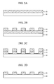
- Figs. 2A to 2D are process diagrams for fabricating a stamp for micro/nano imprint lithography according to the first embodiment of the present invention.
- Fig. 3 is a sequential diagram showing processes for fabricating a stamp for micro/nano imprint lithography according to a second embodiment of the present invention.
- Figs. 4A to 4D are process diagrams for fabricating a stamp for micro/nano imprint lithography according to the second embodiment of the present invention.
- Fig. 5 is a sequential diagram showing processes for fabricating a stamp for micro/nano imprint lithography according to a third embodiment of the present invention.
- Figs. 6A to 6D are process diagrams for fabricating a stamp for micro/nano imprint lithography according to the third embodiment of the present invention.
- Hereinafter, the embodiments of the present invention will be explained in detail by referring to the appended drawings.
- For fabricating a stamp according to a first embodiment of the present invention, as shown in Figs. 1 and 2, a
thin film 15 of diamond-like carbon (DLC) is firstly deposited on a substrate 10 (S11). - The deposition of the DLC
thin film 15 may be carried out by a process selected from ion plating, plasma chemical vapor deposition (CVD) using direct current (DC) or radio frequency (RF), sputtering using DC, RF or ion-beam, and laser synthesis. - The
substrate 10 may be made of a light-transmittable material that may be one of, for example, quartz, glass, diamond, a transparent polymer and a transparent semiconductor such as indium tin oxide (ITO). In an ultraviolet (UV) micro/nano imprint lithography process, in particular, thesubstrate 10 partly composing the stamp is preferably made of a light-transmittable material in order to transmit ultraviolet ray through the stamp. Thesubstrate 10 for thermal imprint may be made of one of an opaque wafer, a semiconductor compound, a polymer, a ceramic material and materials above-mentioned. - The DLC film is one of non-crystalline solid-phase carbon films that are as excellent as diamond in hardness, wear resistance, lubrication, electrical insulation, chemical stability and optical property. The DLC film is good in hydrophobic property and is capable of light-transmittance, especially UV ray- transmittance.
- The hardness of the DLC film varies widely according to the synthesizing condition and is on the whole as high as silicon carbide (SiC) or aluminum oxide (Al2O3).
- The DLC film has a very low friction coefficient. The friction coefficient of the DLC film measured by a scratch tester using a diamond tip varies in the range of 0.04 to 0.06, which is lower by about 30 % than that of glass. The friction coefficient between diamond and the film or the film and the film is not dependent on humidity. However, the friction coefficient between the steel ball and the film is strongly dependent on humidity. Also, the friction coefficient decreases to a value as low as 0.00 to 0.02 as humidity decreases.
- The DLC film has so excellent in chemical stability that it does not react with the most of acid or organic solvent, and no damage is found on the coating even in 80 % aqua regia.
- The most eminent electrical property of the DLC film is a high resistivity. The resistivity is in the wide range of 104 to 1014 ohms (Ω) according to the synthesizing condition.
- On the other hand, a fluorine (F) gas may be added or a fluoro group (F) may be included by sputtering the solid substrate containing a fluoro group (F) in order to improve the hydrophobic property of the DLC
thin film 15. When a gas including a fluoro group (F) such as octafluorocyclobutane (C4F8), hexafluoroethane (C2F6), tetrafluoromethane (CF4), trifluoromethane (CHF3), sulfur hexafluoride (SF6) is properly supplied at the time of the deposition of DLCthin film 15, the fluoro group (F) is positioned tangled inside the DLCthin film 15. Also, fluorocarbon resins, for example Teflon polytetrafluoroethylene (PTFE) may be used as the solid substrate for a target. - Next, a resist 18 is applied on top of the DLC thin film 15 (S12). Photoresist may be used as the resist 18.
- Then the resist 18 is patterned (S13). Electron-beam lithography or ion-beam lithography may be used for patterning the resist 18.
- According to the electron-beam lithography process, first the electron-beam scans along a wanted pattern on the photoresist that shows chemical changes by the exposure to the electron-beam. Secondly, the patterning of the resist 18 is carried out through developing by removing or leaving the exposed area selectively.
- According to the ion-beam lithography process, the resist 18 may be patterned by the ion-beam instead of the electron beam in a similar way to the electron-beam lithography process
- Next, the DLC
thin film 15 is etched by using the patterned resist 18 as a protective layer (S14). - The plasma etching process including reactive ion etching (RIE) is used for etching the DLC
thin film 15. - According to the reactive ion etching process, an etch-resistant etching mask is used, and an anisotropic etching is carried out by using a gas with high selectivity ratio.
- First, plasma is formed in the area of the DLC
thin film 15 to be removed, and electric potential formed outside starts sputtering. Discharge inside the plasma produces chemical reactant from a gas poured in. Selected as the etching gas may be a gas that is capable of producing a volatile by-product by reacting with the diamond-like carbon to be removed. - Next, the resist 18 is removed (S15).
- The stamp for micro/nano imprint lithography of the present embodiment is finished by removing the resist 18 covering the patterned DLC
thin film 15. Therefore, the micro/nano-structure of the stamp is made of the DLCthin film 15. The stamp made as above may be used for thermal micro/nano imprint lithography as well as UV micro/nano imprint lithography. - Fig. 3 is a sequential diagram showing processes for fabricating a stamp for micro/nano imprint lithography according to a second embodiment of the present invention, and Figs. 4A to 4D are process diagrams for fabricating a stamp for micro/nano imprint lithography according to the second embodiment of the present invention.
- For fabricating a stamp according to the present embodiment, a first
thin film 25 of diamond-like carbon (DLC) is firstly deposited on a substrate 10 (S21). - The deposition of the DLC
thin film 25 may be carried out by one process selected from ion plating, plasma chemical vapor deposition (CVD) using direct current (DC) or radio frequency (RF), sputtering using DC, RF or ion-beam, and laser synthesis. - The
substrate 10 may be made of a light-transmittable material that may be one of, for example, quartz, glass, diamond, a transparent polymer and a transparent semiconductor such as indium tin oxide (ITO). In an ultraviolet (UV) micro/nano imprint lithography process, in particular, thesubstrate 10 partly composing the stamp is preferably made of a light-transmittable material in order to transmit ultraviolet ray through the stamp. Thesubstrate 10 for thermal imprint may be made of one of an opaque wafer, a semiconductor compound, a polymer, a ceramic material and materials above-mentioned. - The first DLC
thin film 25 may be a material having the same properties as the DLC thin film used in the first embodiment. In order to improve the hydrophobic property of the first DLCthin film 25, a fluorine (F) gas may be added or a fluoro group (F) may be included by sputtering the solid substrate containing a fluoro group (F). - Next, a resist 28 is applied on top of the first DLC thin film 25 (S22). Photoresist may be used as the resist 28.
- Then the resist 28 is patterned (S23). Electron-beam lithography or ion-beam lithography may be used for patterning the resist 28.
- Then, a second DLC
thin film 29 is deposited on top of the patterned resist 28 and on the first DLCthin film 25 exposed through openings of the patterned resist 28 (S24). - In other words, the openings and the cover parts are formed by patterning the resist 28. The cover part of the resist 28 serves to cover and hide the first DLC
thin film 25, and the opening of the resist 28 serves to expose the first DLCthin film 25. At the time of deposition of the second DLCthin film 29 over the patterned resist 28, the second DLCthin film 29 is deposited on top of the first DLCthin film 25 exposed through openings as well as on top of the cover parts of the resist 28. - In order to improve the hydrophobic property of the second DLC
thin film 29, a fluorine (F) gas may be added or a fluoro group (F) may be included by sputtering the solid substrate containing a fluoro group (F). - Next, the resist 28 is removed (S25).
- In the step to remove the resist 28, the second DLC
thin film 29b deposited on the resist 28 is removed together. Therefore, only the second DLCthin film 29a deposited on the first DLCthin film 25 remains so as to form the micro/nano-structure after the resist 28 is removed. That is the finished stamp of the micro/nano imprint lithography of the present embodiment. The stamp made as above may be used for thermal micro/nano imprint lithography as well as UV micro/nano imprint lithography. - Fig. 5 is a sequential diagram showing processes for fabricating a stamp for micro/nano imprint lithography according to a third embodiment of the present invention, and Figs. 6A to 6D are process diagrams for fabricating a stamp for micro/nano imprint lithography according to the third embodiment of the present invention.
- For fabricating a stamp according to the present embodiment, a first
thin film 35 of diamond-like carbon (DLC) is firstly deposited on a substrate 10 (S31). - The deposition of the DLC
thin film 35 may be carried out by one process selected from ion plating, plasma chemical vapor deposition (CVD) using direct current (DC) or radio frequency (RF), sputtering using DC, RF or ion-beam, and laser synthesis. - The
substrate 10 may be made of a light-transmittable material that may be one of, for example, quartz, glass, diamond, a transparent polymer and a transparent semiconductor such as indium tin oxide (ITO). In an ultraviolet (UV) micro/nano imprint lithography process, in particular, thesubstrate 10 partly composing the stamp is preferably made of a light-transmittable material in order to transmit ultraviolet ray through the stamp. Thesubstrate 10 for thermal imprint may be made of one of an opaque wafer, a semiconductor compound, a polymer, a ceramic material and materials above-mentioned. - The first DLC
thin film 35 may be a material having the same properties as the DLC thin film used in the first embodiment. In order to improve the hydrophobic property of the first DLCthin film 35, a fluorine (F) gas may be added or a fluoro group (F) may be included by sputtering the solid substrate containing a fluoro group (F). - Next, micro/nano-
structures 37 are formed on the first DLC thin film 35 (S32). The micro/nano-structures 37 may be made of a resin material. - Then, a second DLC
thin film 39 is deposited to encompass the micro/nano-structures 37 (S33). - In this process, a fluorine (F) gas may be added or a fluoro group (F) may be included by sputtering the solid substrate containing a fluoro group (F) in order to improve the hydrophobic property of the second DLC
thin film 39, - The stamp for micro/nano imprint lithography of the present embodiment is finished by coating the micro/nano-
structures 37 with the second DLCthin film 39. The stamp made as above may be applied for thermal micro/nano imprint lithography as well as UV micro/nano imprint lithography. - Although an embodiment of the present invention have been described in detail hereinabove, it should be clearly understood that many variations and/or modifications of the basic inventive concepts herein taught which may appear to those skilled in the present art will still fall within the spirit and scope of the present invention, as defined in the appended claims.
Claims (20)
- A method for fabricating a stamp for micro/nano imprint lithography comprising:depositing a thin film of diamond-like carbon on a substrate;applying resist on the diamond-like carbon thin film;patterning the resist;etching the diamond-like carbon thin film by using the resist as a protective layer; andremoving the resist.
- The method for fabricating a stamp for micro/nano imprint lithography of claim 1, wherein the deposition in depositing the diamond-like carbon thin film is carried out by a process selected from ion plating, plasma chemical vapor deposition (CVD) using direct current (DC) or radio frequency (RF), sputtering using DC, RF or ion-beam, and laser synthesis.
- The method for fabricating a stamp for micro/nano imprint lithography of claim 1, wherein a gas containing a fluoro group (F) is poured or the diamond-like carbon thin film is deposited on the sputtered solid substrate containing a fluoro group (F) in depositing the diamond-like carbon thin film.
- The method for fabricating a stamp for micro/nano imprint lithography of claim 3, wherein at least one of octafluorocyclobutane (C4F8), hexafluoroethane (C2F6), tetrafluoromethane (CF4), trifluoromethane (CHF3), sulfur hexafluoride (SF6) is selected as a pouring gas including a fluoro group (F).
- The method for fabricating a stamp for micro/nano imprint lithography of claim 3, wherein fluorocarbon resins is used as a target for the solid substrate including a fluoro group (F).
- The method for fabricating a stamp for micro/nano imprint lithography of claim 5, wherein the fluorocarbon resins is polytetrafluoroethylene (PTFE).
- The method for fabricating a stamp for micro/nano imprint lithography of claim 1, wherein the diamond-like carbon thin film is etched by plasma etching process including reactive ion etching (RIE).
- A method for fabricating a stamp for micro/nano imprint lithography comprising:depositing a first thin film of diamond-like carbon on a substrate;applying resist on the first diamond-like carbon thin film;patterning the resist;depositing a second diamond-like carbon thin film on top of the patterned resist and on the first diamond-like carbon thin film exposed through openings of the patterned resist; andremoving the resist.
- The method for fabricating a stamp for micro/nano imprint lithography of claim 8, wherein a gas containing a fluoro group (F) is poured or the first diamond-like carbon thin film is deposited on the sputtered solid substrate containing a fluoro group (F) in depositing the first diamond-like carbon thin film.
- The method for fabricating a stamp for micro/nano imprint lithography of claim 8, wherein a gas containing a fluoro group (F) is poured or the second diamond-like carbon thin film is deposited on the sputtered solid substrate containing a fluoro group (F) in depositing the second diamond-like carbon thin film.
- The method for fabricating a stamp for micro/nano imprint lithography of claim 8, wherein the diamond-like carbon thin film is etched by plasma etching process including reactive ion etching (RIE).
- The method for fabricating a stamp for micro/nano imprint lithography of claim 8, wherein both of the resist and the second diamond-like carbon thin film deposited on the resist are removed together in the step to remove the resist.
- A method for fabricating a stamp for micro/nano imprint lithography comprising:depositing a first thin film of diamond-like carbon on a substrate;forming micro/nano-structures on top of the first diamond-like carbon thin film; anddepositing a second diamond-like carbon thin film to encompass the micro/nano-structures.
- The method for fabricating a stamp for micro/nano imprint lithography of claim 13, wherein the micro/nano-structures are made of a resin material.
- The method for fabricating a stamp for micro/nano imprint lithography of claim 13, wherein a gas containing a fluoro group (F) is poured or the first diamond-like carbon thin film is deposited on the sputtered solid substrate containing a fluoro group (F) in depositing the first diamond-like carbon thin film.
- The method for fabricating a stamp for micro/nano imprint lithography of claim 13, wherein a gas containing a fluoro group (F) is poured or the second diamond-like carbon thin film is deposited on the sputtered solid substrate containing a fluoro group (F) in depositing the second diamond-like carbon thin film.
- A stamp for micro/nano imprint lithography, the stamp used in the micro/nano imprint lithography process, comprising:a substrate; anda micro/nano-structure formed of diamond-like carbon thin film on top of the substrate.
- The stamp for micro/nano imprint lithography of claim 17, wherein the micro/nano-structure made of diamond-like carbon thin film includes a fluoro group (F).
- The stamp for micro/nano imprint lithography of claim 17, wherein a first diamond-like carbon thin film is formed on the substrate, and the micro/nano-structure is formed by a second diamond-like carbon thin film patterned on top of the first diamond-like carbon thin film.
- The stamp for micro/nano imprint lithography of claim 17, wherein the micro/nano-structure is formed by coating the structure made of a resin material with diamond-like carbon thin film.
Applications Claiming Priority (1)
| Application Number | Priority Date | Filing Date | Title |
|---|---|---|---|
| KR1020050098080A KR100772639B1 (en) | 2005-10-18 | 2005-10-18 | Stamp for fine imprint lithography using diamond-like carbon thin film and its manufacturing method |
Publications (3)
| Publication Number | Publication Date |
|---|---|
| EP1785770A2 true EP1785770A2 (en) | 2007-05-16 |
| EP1785770A3 EP1785770A3 (en) | 2007-07-11 |
| EP1785770B1 EP1785770B1 (en) | 2009-11-11 |
Family
ID=37814633
Family Applications (1)
| Application Number | Title | Priority Date | Filing Date |
|---|---|---|---|
| EP06021860A Not-in-force EP1785770B1 (en) | 2005-10-18 | 2006-10-18 | Method for fabricating a stamp for micro/nano imprint lithography |
Country Status (6)
| Country | Link |
|---|---|
| US (1) | US7914693B2 (en) |
| EP (1) | EP1785770B1 (en) |
| JP (1) | JP2007116163A (en) |
| KR (1) | KR100772639B1 (en) |
| AT (1) | ATE448507T1 (en) |
| DE (1) | DE602006010307D1 (en) |
Cited By (2)
| Publication number | Priority date | Publication date | Assignee | Title |
|---|---|---|---|---|
| CN101118378B (en) * | 2007-08-22 | 2010-08-25 | 武汉工程大学 | Preparation method of diamond surface patterning |
| EP2163367A4 (en) * | 2007-06-04 | 2011-03-23 | Maruzen Petrochem Co Ltd | FORM, ARTICLE HAVING SUFFERED MICROTREATMENT AND METHODS OF MAKING SAME |
Families Citing this family (67)
| Publication number | Priority date | Publication date | Assignee | Title |
|---|---|---|---|---|
| JP2007320142A (en) * | 2006-05-31 | 2007-12-13 | Meisho Kiko Kk | Nanoimprint mold |
| KR100889814B1 (en) * | 2006-07-25 | 2009-03-20 | 삼성전자주식회사 | Stamper, manufacturing method and imprinting process of substrate using stamper |
| JP4858030B2 (en) * | 2006-09-13 | 2012-01-18 | 凸版印刷株式会社 | Imprint mold, imprint mold manufacturing method, and pattern forming method |
| US7776628B2 (en) * | 2006-11-16 | 2010-08-17 | International Business Machines Corporation | Method and system for tone inverting of residual layer tolerant imprint lithography |
| JP2009045817A (en) * | 2007-08-20 | 2009-03-05 | Shineisha:Kk | Intaglio and manufacturing method of intaglio |
| US8470701B2 (en) * | 2008-04-03 | 2013-06-25 | Advanced Diamond Technologies, Inc. | Printable, flexible and stretchable diamond for thermal management |
| US8343362B2 (en) * | 2008-12-22 | 2013-01-01 | Kabushiki Kaisha Toshiba | Stamper manufacturing method |
| JP5305388B2 (en) * | 2009-01-16 | 2013-10-02 | トーメイダイヤ株式会社 | Stamper surface material |
| JP4575497B2 (en) * | 2009-01-23 | 2010-11-04 | 株式会社東芝 | Stamper manufacturing method |
| JP5027182B2 (en) * | 2009-04-01 | 2012-09-19 | トーカロ株式会社 | Method for producing imprint mold material and imprint mold material |
| NL2005263A (en) | 2009-09-29 | 2011-03-30 | Asml Netherlands Bv | Imprint lithography. |
| KR20120079734A (en) * | 2011-01-05 | 2012-07-13 | 삼성전자주식회사 | Method of fabricating stamp for nano-imprint |
| KR101069545B1 (en) | 2011-06-20 | 2011-10-05 | 한국기계연구원 | Apparatus and method for manufacturing flexible stamp for imprint lithography |
| US20170110463A1 (en) * | 2011-09-01 | 2017-04-20 | Chengdu Haicun Ip Technology Llc | Imprinted Memory |
| US20130056798A1 (en) * | 2011-09-01 | 2013-03-07 | Chengdu Haicun Ip Technology Llc | Three-Dimensional Printed Memory |
| US20150318475A1 (en) * | 2011-09-01 | 2015-11-05 | Guobiao Zhang | Imprinted Memory |
| US20150117599A1 (en) | 2013-10-31 | 2015-04-30 | Sigray, Inc. | X-ray interferometric imaging system |
| US9623590B2 (en) * | 2012-01-27 | 2017-04-18 | Asahi Kasei E-Materials Corporation | Fine concavo-convex structure product, heat-reactive resist material for dry etching, mold manufacturing method and mold |
| JP6015140B2 (en) * | 2012-06-01 | 2016-10-26 | 大日本印刷株式会社 | Nanoimprint mold and manufacturing method thereof |
| CN103436853B (en) * | 2013-09-04 | 2016-03-16 | 苏州锦元纳米科技有限公司 | Mix fluorine diamond like carbon film, its preparation method and comprise the impression block of this film |
| US9449781B2 (en) | 2013-12-05 | 2016-09-20 | Sigray, Inc. | X-ray illuminators with high flux and high flux density |
| US10269528B2 (en) | 2013-09-19 | 2019-04-23 | Sigray, Inc. | Diverging X-ray sources using linear accumulation |
| US9448190B2 (en) | 2014-06-06 | 2016-09-20 | Sigray, Inc. | High brightness X-ray absorption spectroscopy system |
| US10295485B2 (en) | 2013-12-05 | 2019-05-21 | Sigray, Inc. | X-ray transmission spectrometer system |
| US9570265B1 (en) | 2013-12-05 | 2017-02-14 | Sigray, Inc. | X-ray fluorescence system with high flux and high flux density |
| US10297359B2 (en) | 2013-09-19 | 2019-05-21 | Sigray, Inc. | X-ray illumination system with multiple target microstructures |
| US9390881B2 (en) | 2013-09-19 | 2016-07-12 | Sigray, Inc. | X-ray sources using linear accumulation |
| USRE48612E1 (en) | 2013-10-31 | 2021-06-29 | Sigray, Inc. | X-ray interferometric imaging system |
| US10304580B2 (en) | 2013-10-31 | 2019-05-28 | Sigray, Inc. | Talbot X-ray microscope |
| US9594036B2 (en) | 2014-02-28 | 2017-03-14 | Sigray, Inc. | X-ray surface analysis and measurement apparatus |
| US9823203B2 (en) | 2014-02-28 | 2017-11-21 | Sigray, Inc. | X-ray surface analysis and measurement apparatus |
| JP6167967B2 (en) * | 2014-03-31 | 2017-07-26 | 株式会社島津製作所 | Ultraviolet irradiation device and analyzer equipped with the same |
| US10401309B2 (en) | 2014-05-15 | 2019-09-03 | Sigray, Inc. | X-ray techniques using structured illumination |
| US10352880B2 (en) | 2015-04-29 | 2019-07-16 | Sigray, Inc. | Method and apparatus for x-ray microscopy |
| US10295486B2 (en) | 2015-08-18 | 2019-05-21 | Sigray, Inc. | Detector for X-rays with high spatial and high spectral resolution |
| US10247683B2 (en) | 2016-12-03 | 2019-04-02 | Sigray, Inc. | Material measurement techniques using multiple X-ray micro-beams |
| WO2018175570A1 (en) | 2017-03-22 | 2018-09-27 | Sigray, Inc. | Method of performing x-ray spectroscopy and x-ray absorption spectrometer system |
| US11261085B2 (en) * | 2017-05-03 | 2022-03-01 | Nanotech Security Corp. | Methods for micro and nano fabrication by selective template removal |
| US10578566B2 (en) | 2018-04-03 | 2020-03-03 | Sigray, Inc. | X-ray emission spectrometer system |
| CN111771161B (en) | 2018-05-30 | 2023-07-18 | 株式会社Lg化学 | Photomask for imprinting and manufacturing method thereof |
| CN112424591B (en) | 2018-06-04 | 2024-05-24 | 斯格瑞公司 | Wavelength dispersive X-ray spectrometer |
| US10649119B2 (en) * | 2018-07-16 | 2020-05-12 | Facebook Technologies, Llc | Duty cycle, depth, and surface energy control in nano fabrication |
| DE112019003777B4 (en) | 2018-07-26 | 2025-09-11 | Sigray, Inc. | HIGH BRIGHTNESS X-RAY REFLECTION SOURCE |
| US10656105B2 (en) | 2018-08-06 | 2020-05-19 | Sigray, Inc. | Talbot-lau x-ray source and interferometric system |
| CN112638261B (en) | 2018-09-04 | 2025-06-27 | 斯格瑞公司 | Systems and methods utilizing filtered x-ray fluorescence |
| US11056308B2 (en) | 2018-09-07 | 2021-07-06 | Sigray, Inc. | System and method for depth-selectable x-ray analysis |
| CN109683445A (en) * | 2019-01-10 | 2019-04-26 | 京东方科技集团股份有限公司 | A kind of joining method of nano-pattern, nano impression plate, grating and production method |
| US11342256B2 (en) | 2019-01-24 | 2022-05-24 | Applied Materials, Inc. | Method of fine redistribution interconnect formation for advanced packaging applications |
| JP7403961B2 (en) * | 2019-03-19 | 2023-12-25 | キオクシア株式会社 | Imprint method and semiconductor device manufacturing method |
| IT201900006736A1 (en) | 2019-05-10 | 2020-11-10 | Applied Materials Inc | PACKAGE MANUFACTURING PROCEDURES |
| IT201900006740A1 (en) * | 2019-05-10 | 2020-11-10 | Applied Materials Inc | SUBSTRATE STRUCTURING PROCEDURES |
| US11931855B2 (en) | 2019-06-17 | 2024-03-19 | Applied Materials, Inc. | Planarization methods for packaging substrates |
| US11391950B2 (en) | 2019-06-26 | 2022-07-19 | Meta Platforms Technologies, Llc | Techniques for controlling effective refractive index of gratings |
| CN110456611A (en) * | 2019-09-02 | 2019-11-15 | 无锡微视传感科技有限公司 | Nano-imprint stamp and production method |
| US11862546B2 (en) | 2019-11-27 | 2024-01-02 | Applied Materials, Inc. | Package core assembly and fabrication methods |
| CN112951707A (en) * | 2019-12-11 | 2021-06-11 | 株洲中车时代电气股份有限公司 | Film and preparation method and application thereof |
| US11257790B2 (en) | 2020-03-10 | 2022-02-22 | Applied Materials, Inc. | High connectivity device stacking |
| US11454884B2 (en) | 2020-04-15 | 2022-09-27 | Applied Materials, Inc. | Fluoropolymer stamp fabrication method |
| US11400545B2 (en) | 2020-05-11 | 2022-08-02 | Applied Materials, Inc. | Laser ablation for package fabrication |
| CN112011784B (en) * | 2020-06-29 | 2022-09-20 | 南方科技大学 | Ordered patterned porous diamond film and preparation method and application thereof |
| US11232951B1 (en) | 2020-07-14 | 2022-01-25 | Applied Materials, Inc. | Method and apparatus for laser drilling blind vias |
| US11676832B2 (en) | 2020-07-24 | 2023-06-13 | Applied Materials, Inc. | Laser ablation system for package fabrication |
| US11521937B2 (en) | 2020-11-16 | 2022-12-06 | Applied Materials, Inc. | Package structures with built-in EMI shielding |
| US11404318B2 (en) | 2020-11-20 | 2022-08-02 | Applied Materials, Inc. | Methods of forming through-silicon vias in substrates for advanced packaging |
| US11705365B2 (en) | 2021-05-18 | 2023-07-18 | Applied Materials, Inc. | Methods of micro-via formation for advanced packaging |
| US12183684B2 (en) | 2021-10-26 | 2024-12-31 | Applied Materials, Inc. | Semiconductor device packaging methods |
| CN114551702B (en) * | 2022-02-25 | 2025-02-21 | 连云港杰瑞电子有限公司 | LED lamp radiator, manufacturing method of the radiator and LED lamp |
Family Cites Families (17)
| Publication number | Priority date | Publication date | Assignee | Title |
|---|---|---|---|---|
| JP2800274B2 (en) | 1989-06-16 | 1998-09-21 | 日本電気株式会社 | Stamper |
| JP3189347B2 (en) * | 1991-12-24 | 2001-07-16 | 住友電気工業株式会社 | Resin mold, resin mold manufacturing method, and resin molding method |
| JPH1096808A (en) | 1996-09-24 | 1998-04-14 | Nippon Telegr & Teleph Corp <Ntt> | Fine pattern formation method |
| JP3062163B2 (en) * | 1998-12-01 | 2000-07-10 | キヤノン販売株式会社 | Semiconductor device and method for forming film of semiconductor device |
| WO2001040537A1 (en) * | 1999-11-30 | 2001-06-07 | The Regents Of The University Of California | Method for producing fluorinated diamond-like carbon films |
| KR100944313B1 (en) | 2002-01-25 | 2010-02-24 | 제이에스알 가부시끼가이샤 | 2-layer laminated film and pattern formation method using the same |
| JP2004130775A (en) | 2002-08-09 | 2004-04-30 | Maxell Hi Tec Ltd | Injection molding machine, constituent member for use in the same, and surface treatment method |
| JP2004164689A (en) * | 2002-11-08 | 2004-06-10 | Ricoh Co Ltd | Direct mastering substrate manufacturing method, direct mastering substrate, and stamper manufacturing method |
| US6858909B2 (en) * | 2002-11-29 | 2005-02-22 | International Business Machines Corporation | CMP assisted liftoff micropatterning |
| KR100488049B1 (en) | 2003-01-16 | 2005-05-06 | 엘지전자 주식회사 | nano imprint fabrication method |
| JP2004311713A (en) | 2003-04-07 | 2004-11-04 | Mitsubishi Electric Corp | Mold for manufacturing semiconductor devices |
| JP2005047080A (en) | 2003-07-31 | 2005-02-24 | Alps Electric Co Ltd | Resin optical component molding die having fine uneven surface and method of manufacturing resin optical component using the same |
| US20050084804A1 (en) | 2003-10-16 | 2005-04-21 | Molecular Imprints, Inc. | Low surface energy templates |
| JP4257848B2 (en) | 2003-12-26 | 2009-04-22 | 独立行政法人産業技術総合研究所 | Mold and manufacturing method thereof |
| US7309515B2 (en) * | 2004-02-04 | 2007-12-18 | Industrial Technology Research Institute | Method for fabricating an imprint mold structure |
| JP2006032423A (en) | 2004-07-12 | 2006-02-02 | Toshiba Corp | Stamper for imprint processing and manufacturing method thereof |
| US7186574B2 (en) * | 2004-09-30 | 2007-03-06 | Hitachi Global Storage Technologies Netherlands B.V. | CMP process metrology test structures |
-
2005
- 2005-10-18 KR KR1020050098080A patent/KR100772639B1/en not_active Expired - Fee Related
-
2006
- 2006-10-18 EP EP06021860A patent/EP1785770B1/en not_active Not-in-force
- 2006-10-18 AT AT06021860T patent/ATE448507T1/en active
- 2006-10-18 DE DE602006010307T patent/DE602006010307D1/en active Active
- 2006-10-18 US US11/582,461 patent/US7914693B2/en active Active
- 2006-10-18 JP JP2006284320A patent/JP2007116163A/en active Pending
Cited By (2)
| Publication number | Priority date | Publication date | Assignee | Title |
|---|---|---|---|---|
| EP2163367A4 (en) * | 2007-06-04 | 2011-03-23 | Maruzen Petrochem Co Ltd | FORM, ARTICLE HAVING SUFFERED MICROTREATMENT AND METHODS OF MAKING SAME |
| CN101118378B (en) * | 2007-08-22 | 2010-08-25 | 武汉工程大学 | Preparation method of diamond surface patterning |
Also Published As
| Publication number | Publication date |
|---|---|
| KR20070042309A (en) | 2007-04-23 |
| EP1785770B1 (en) | 2009-11-11 |
| EP1785770A3 (en) | 2007-07-11 |
| JP2007116163A (en) | 2007-05-10 |
| US20070158872A1 (en) | 2007-07-12 |
| ATE448507T1 (en) | 2009-11-15 |
| US7914693B2 (en) | 2011-03-29 |
| DE602006010307D1 (en) | 2009-12-24 |
| KR100772639B1 (en) | 2007-11-02 |
Similar Documents
| Publication | Publication Date | Title |
|---|---|---|
| US7914693B2 (en) | Stamp for micro/nano imprint lithography using diamond-like carbon and method of fabricating the same | |
| EP1364253B1 (en) | Method of forming lithographic template and use of it | |
| US7309515B2 (en) | Method for fabricating an imprint mold structure | |
| KR101018519B1 (en) | Multilayer lithography template and its manufacturing method | |
| US7279113B2 (en) | Method of forming a compliant template for UV imprinting | |
| US20080138460A1 (en) | Multilayer nano imprint lithography | |
| US7906274B2 (en) | Method of creating a template employing a lift-off process | |
| US20050084804A1 (en) | Low surface energy templates | |
| KR101789921B1 (en) | Method of manufacturing a nano thin-layer pattern structure | |
| US20060145398A1 (en) | Release layer comprising diamond-like carbon (DLC) or doped DLC with tunable composition for imprint lithography templates and contact masks | |
| KR20120067170A (en) | Method of manufacturing stamp for nanoimprint | |
| US20060110914A1 (en) | Direct imprinting of etch barriers using step and flash imprint lithography | |
| del Campo et al. | Generating micro-and nanopatterns on polymeric materials | |
| JP2005159358A (en) | Nanoimprint lithography method and substrate | |
| US8512585B2 (en) | Template pillar formation | |
| KR100488049B1 (en) | nano imprint fabrication method | |
| Chen et al. | Bi-Layer nanoimprinting lithography for metal-assisted chemical etching with application on silicon mold replication | |
| Tiginyanu et al. | Nanoimprint lithography (NIL) and related techniques for electronics applications | |
| KR20190133369A (en) | Lithography Method Using Scanning Probe Microscope | |
| Low et al. | Combinatorial-mold imprint lithography: A versatile technique for fabrication of three-dimensional polymer structures | |
| JP2005313647A (en) | Molds for nanoprinting, methods for producing such molds, and methods of using such molds | |
| Acikgoz et al. | Nanoscale patterning by UV nanoimprint lithography using an organometallic resist | |
| KR101389048B1 (en) | Method for fabricating patterns on the glass | |
| Mohamed | Three-dimensional patterning using ultraviolet curable nanoimprint lithography | |
| JP2012061599A (en) | Application of benzocyclobutene resin to imprint technology, and method for forming pattern by the technology |
Legal Events
| Date | Code | Title | Description |
|---|---|---|---|
| PUAI | Public reference made under article 153(3) epc to a published international application that has entered the european phase |
Free format text: ORIGINAL CODE: 0009012 |
|
| 17P | Request for examination filed |
Effective date: 20061018 |
|
| AK | Designated contracting states |
Kind code of ref document: A2 Designated state(s): AT BE BG CH CY CZ DE DK EE ES FI FR GB GR HU IE IS IT LI LT LU LV MC NL PL PT RO SE SI SK TR |
|
| AX | Request for extension of the european patent |
Extension state: AL BA HR MK YU |
|
| PUAL | Search report despatched |
Free format text: ORIGINAL CODE: 0009013 |
|
| RIN1 | Information on inventor provided before grant (corrected) |
Inventor name: KIM, KIN-DON Inventor name: CHOI, DAE-GEUN,SONGLIM APT. Inventor name: JEONG, JUN-HO Inventor name: LEE, EUNG-SUG Inventor name: SIM, YOUNG-SUK |
|
| AK | Designated contracting states |
Kind code of ref document: A3 Designated state(s): AT BE BG CH CY CZ DE DK EE ES FI FR GB GR HU IE IS IT LI LT LU LV MC NL PL PT RO SE SI SK TR |
|
| AX | Request for extension of the european patent |
Extension state: AL BA HR MK YU |
|
| 17Q | First examination report despatched |
Effective date: 20070914 |
|
| AKX | Designation fees paid |
Designated state(s): AT CH DE GB LI NL SE |
|
| GRAP | Despatch of communication of intention to grant a patent |
Free format text: ORIGINAL CODE: EPIDOSNIGR1 |
|
| RTI1 | Title (correction) |
Free format text: METHOD FOR FABRICATING A STAMP FOR MICRO/NANO IMPRINT LITHOGRAPHY |
|
| GRAS | Grant fee paid |
Free format text: ORIGINAL CODE: EPIDOSNIGR3 |
|
| GRAA | (expected) grant |
Free format text: ORIGINAL CODE: 0009210 |
|
| AK | Designated contracting states |
Kind code of ref document: B1 Designated state(s): AT CH DE GB LI NL SE |
|
| REG | Reference to a national code |
Ref country code: GB Ref legal event code: FG4D |
|
| REG | Reference to a national code |
Ref country code: CH Ref legal event code: EP |
|
| REF | Corresponds to: |
Ref document number: 602006010307 Country of ref document: DE Date of ref document: 20091224 Kind code of ref document: P |
|
| REG | Reference to a national code |
Ref country code: SE Ref legal event code: TRGR |
|
| NLV1 | Nl: lapsed or annulled due to failure to fulfill the requirements of art. 29p and 29m of the patents act | ||
| PLBE | No opposition filed within time limit |
Free format text: ORIGINAL CODE: 0009261 |
|
| STAA | Information on the status of an ep patent application or granted ep patent |
Free format text: STATUS: NO OPPOSITION FILED WITHIN TIME LIMIT |
|
| 26N | No opposition filed |
Effective date: 20100812 |
|
| REG | Reference to a national code |
Ref country code: CH Ref legal event code: PL |
|
| GBPC | Gb: european patent ceased through non-payment of renewal fee |
Effective date: 20101018 |
|
| PG25 | Lapsed in a contracting state [announced via postgrant information from national office to epo] |
Ref country code: CH Free format text: LAPSE BECAUSE OF NON-PAYMENT OF DUE FEES Effective date: 20101031 Ref country code: LI Free format text: LAPSE BECAUSE OF NON-PAYMENT OF DUE FEES Effective date: 20101031 |
|
| PG25 | Lapsed in a contracting state [announced via postgrant information from national office to epo] |
Ref country code: GB Free format text: LAPSE BECAUSE OF NON-PAYMENT OF DUE FEES Effective date: 20101018 |
|
| PG25 | Lapsed in a contracting state [announced via postgrant information from national office to epo] |
Ref country code: NL Free format text: LAPSE BECAUSE OF FAILURE TO SUBMIT A TRANSLATION OF THE DESCRIPTION OR TO PAY THE FEE WITHIN THE PRESCRIBED TIME-LIMIT Effective date: 20091111 |
|
| REG | Reference to a national code |
Ref country code: DE Ref legal event code: R082 Ref document number: 602006010307 Country of ref document: DE Representative=s name: ROOS, PETER, DIPL.-PHYS.UNIV. DR.RER.NAT., DE |
|
| PGFP | Annual fee paid to national office [announced via postgrant information from national office to epo] |
Ref country code: DE Payment date: 20141014 Year of fee payment: 9 Ref country code: SE Payment date: 20141013 Year of fee payment: 9 |
|
| PGFP | Annual fee paid to national office [announced via postgrant information from national office to epo] |
Ref country code: AT Payment date: 20140925 Year of fee payment: 9 |
|
| REG | Reference to a national code |
Ref country code: DE Ref legal event code: R119 Ref document number: 602006010307 Country of ref document: DE |
|
| REG | Reference to a national code |
Ref country code: SE Ref legal event code: EUG |
|
| REG | Reference to a national code |
Ref country code: AT Ref legal event code: MM01 Ref document number: 448507 Country of ref document: AT Kind code of ref document: T Effective date: 20151018 |
|
| PG25 | Lapsed in a contracting state [announced via postgrant information from national office to epo] |
Ref country code: DE Free format text: LAPSE BECAUSE OF NON-PAYMENT OF DUE FEES Effective date: 20160503 |
|
| PG25 | Lapsed in a contracting state [announced via postgrant information from national office to epo] |
Ref country code: SE Free format text: LAPSE BECAUSE OF NON-PAYMENT OF DUE FEES Effective date: 20151019 Ref country code: AT Free format text: LAPSE BECAUSE OF NON-PAYMENT OF DUE FEES Effective date: 20151018 |