EP1783739A2 - Data driving circuit and electroluminescent display using the same - Google Patents
Data driving circuit and electroluminescent display using the same Download PDFInfo
- Publication number
- EP1783739A2 EP1783739A2 EP06255725A EP06255725A EP1783739A2 EP 1783739 A2 EP1783739 A2 EP 1783739A2 EP 06255725 A EP06255725 A EP 06255725A EP 06255725 A EP06255725 A EP 06255725A EP 1783739 A2 EP1783739 A2 EP 1783739A2
- Authority
- EP
- European Patent Office
- Prior art keywords
- data
- driving circuit
- signals
- stage
- node
- Prior art date
- Legal status (The legal status is an assumption and is not a legal conclusion. Google has not performed a legal analysis and makes no representation as to the accuracy of the status listed.)
- Granted
Links
Images


Classifications
-
- G—PHYSICS
- G09—EDUCATION; CRYPTOGRAPHY; DISPLAY; ADVERTISING; SEALS
- G09G—ARRANGEMENTS OR CIRCUITS FOR CONTROL OF INDICATING DEVICES USING STATIC MEANS TO PRESENT VARIABLE INFORMATION
- G09G3/00—Control arrangements or circuits, of interest only in connection with visual indicators other than cathode-ray tubes
- G09G3/20—Control arrangements or circuits, of interest only in connection with visual indicators other than cathode-ray tubes for presentation of an assembly of a number of characters, e.g. a page, by composing the assembly by combination of individual elements arranged in a matrix no fixed position being assigned to or needed to be assigned to the individual characters or partial characters
- G09G3/22—Control arrangements or circuits, of interest only in connection with visual indicators other than cathode-ray tubes for presentation of an assembly of a number of characters, e.g. a page, by composing the assembly by combination of individual elements arranged in a matrix no fixed position being assigned to or needed to be assigned to the individual characters or partial characters using controlled light sources
- G09G3/30—Control arrangements or circuits, of interest only in connection with visual indicators other than cathode-ray tubes for presentation of an assembly of a number of characters, e.g. a page, by composing the assembly by combination of individual elements arranged in a matrix no fixed position being assigned to or needed to be assigned to the individual characters or partial characters using controlled light sources using electroluminescent panels
- G09G3/32—Control arrangements or circuits, of interest only in connection with visual indicators other than cathode-ray tubes for presentation of an assembly of a number of characters, e.g. a page, by composing the assembly by combination of individual elements arranged in a matrix no fixed position being assigned to or needed to be assigned to the individual characters or partial characters using controlled light sources using electroluminescent panels semiconductive, e.g. using light-emitting diodes [LED]
- G09G3/3208—Control arrangements or circuits, of interest only in connection with visual indicators other than cathode-ray tubes for presentation of an assembly of a number of characters, e.g. a page, by composing the assembly by combination of individual elements arranged in a matrix no fixed position being assigned to or needed to be assigned to the individual characters or partial characters using controlled light sources using electroluminescent panels semiconductive, e.g. using light-emitting diodes [LED] organic, e.g. using organic light-emitting diodes [OLED]
- G09G3/3275—Details of drivers for data electrodes
-
- G—PHYSICS
- G09—EDUCATION; CRYPTOGRAPHY; DISPLAY; ADVERTISING; SEALS
- G09G—ARRANGEMENTS OR CIRCUITS FOR CONTROL OF INDICATING DEVICES USING STATIC MEANS TO PRESENT VARIABLE INFORMATION
- G09G3/00—Control arrangements or circuits, of interest only in connection with visual indicators other than cathode-ray tubes
- G09G3/20—Control arrangements or circuits, of interest only in connection with visual indicators other than cathode-ray tubes for presentation of an assembly of a number of characters, e.g. a page, by composing the assembly by combination of individual elements arranged in a matrix no fixed position being assigned to or needed to be assigned to the individual characters or partial characters
-
- G—PHYSICS
- G11—INFORMATION STORAGE
- G11C—STATIC STORES
- G11C19/00—Digital stores in which the information is moved stepwise, e.g. shift registers
- G11C19/18—Digital stores in which the information is moved stepwise, e.g. shift registers using capacitors as main elements of the stages
- G11C19/182—Digital stores in which the information is moved stepwise, e.g. shift registers using capacitors as main elements of the stages in combination with semiconductor elements, e.g. bipolar transistors, diodes
- G11C19/184—Digital stores in which the information is moved stepwise, e.g. shift registers using capacitors as main elements of the stages in combination with semiconductor elements, e.g. bipolar transistors, diodes with field-effect transistors, e.g. MOS-FET
-
- G—PHYSICS
- G11—INFORMATION STORAGE
- G11C—STATIC STORES
- G11C19/00—Digital stores in which the information is moved stepwise, e.g. shift registers
- G11C19/28—Digital stores in which the information is moved stepwise, e.g. shift registers using semiconductor elements
-
- G—PHYSICS
- G09—EDUCATION; CRYPTOGRAPHY; DISPLAY; ADVERTISING; SEALS
- G09G—ARRANGEMENTS OR CIRCUITS FOR CONTROL OF INDICATING DEVICES USING STATIC MEANS TO PRESENT VARIABLE INFORMATION
- G09G2310/00—Command of the display device
- G09G2310/02—Addressing, scanning or driving the display screen or processing steps related thereto
- G09G2310/0264—Details of driving circuits
- G09G2310/027—Details of drivers for data electrodes, the drivers handling digital grey scale data, e.g. use of D/A converters
-
- G—PHYSICS
- G09—EDUCATION; CRYPTOGRAPHY; DISPLAY; ADVERTISING; SEALS
- G09G—ARRANGEMENTS OR CIRCUITS FOR CONTROL OF INDICATING DEVICES USING STATIC MEANS TO PRESENT VARIABLE INFORMATION
- G09G2310/00—Command of the display device
- G09G2310/02—Addressing, scanning or driving the display screen or processing steps related thereto
- G09G2310/0264—Details of driving circuits
- G09G2310/0286—Details of a shift registers arranged for use in a driving circuit
-
- G—PHYSICS
- G09—EDUCATION; CRYPTOGRAPHY; DISPLAY; ADVERTISING; SEALS
- G09G—ARRANGEMENTS OR CIRCUITS FOR CONTROL OF INDICATING DEVICES USING STATIC MEANS TO PRESENT VARIABLE INFORMATION
- G09G2330/00—Aspects of power supply; Aspects of display protection and defect management
- G09G2330/02—Details of power systems and of start or stop of display operation
- G09G2330/021—Power management, e.g. power saving
Abstract
Description
- The present invention relates to a driving circuit for driving active matrix displays. More particularly, the present invention relates to a data driving circuit that applies a data signal to an electroluminescent display. The present invention also relates to an electroluminescent display.
- Active matrix displays, such as an electroluminescent display, may include a pixel array arranged in the form of a matrix composed of cross points between the data lines and the scan lines, i.e., a matrix pixel unit. That is, the data lines may constitute vertical lines (i.e., column lines) of the matrix pixel unit and the scan lines may constitute horizontal lines (i.e., row lines) of the matrix pixel unit. The data driving circuit may supply data signals into the matrix pixel unit at a predetermined time.
- FIG. 1 illustrates a block diagram of an exemplary configuration of a data driving circuit. Referring to FIG. 1, a data driving circuit may include a
shift register 10, alatch unit 20 and a D/A converter 30. - The
shift register 10 may receive a start pulse (/CLK) and a clock (CLK) signal to generate a plurality of shift signals. The shift signals may be generated sequentially and transmitted to alatch unit 20. Thelatch unit 20 may receive data signals, e.g., video data, and the shift signals. A sampling latch may receive the data signals in series and may output the shift signals in parallel. Accordingly, a row of data signals may be simultaneously applied to a row of pixel units (not illustrated). - The D/
A converter unit 30 may convert data signals, output as digital data signals from thelatch unit 20, into analog data signals. The D/A converter unit 30 then may output the analog data signals to a pixel unit (not illustrated). The digital data signals converted into the analog data signals may be used to display colors according to a grey level ratio. - FIG. 2 illustrates an exemplary configuration of a shift register, which may be used in the data driving circuit illustrated in FIG. 1. Referring to FIG. 2, the shift register may use a master-slave flip/flop arrangement. In an exemplary operation, the shift register may receive and output signals when the clock is at a low level; the shift register may not output signals when the clock is at a high level.
- In this exemplary circuit, a problem may exist because the inverters may output a static current when its input is at a low level. Also, the static current may be generated in half of the inverters inside the flip/flop. Therefore, the overall power consumption of the circuit may be increased since the number of inverters receiving a high-level input in the flip/flop may be the same as the number of inverters receiving a low level input.
- A high level output voltage may be calculated by accounting for the voltage and a resistance that may exist between a supply voltage potential and ground, and the low level output voltage may be higher than a threshold voltage of a transistor, as illustrated in FIG. 2. In other words, the high level input voltage received at every stage may vary according to property deviations of the transistors. Therefore, the circuit may operate erroneously due to these level variations generated at the high level. Also, a low-level deviation of the output voltage may be represented by an ON resistance deviation of input transistors in the inverters illustrated in the circuit of FIG. 2, which may increase a high-level deviation of the input voltage. Transistors, for example, that may be employed in an electroluminescent display may make the above problems even worse due to the substantial property deviations that may exist.
- Additionally, an inverter may charge an output port by allowing a current to flow through an input transistor to the output port. The output port may discharge by allowing a current to flow from the output port to a load transistor. Accordingly, a source-gate voltage of the load transistor may be gradually reduced when the output port is being charged. Therefore, the discharge current may fluctuate and the efficiency of the discharge may be deteriorated.
- The present invention sets out to provide a data driving circuit and an electroluminescent display employing the same, which substantially overcome one or more of the above described problems arising from the limitations and disadvantages of the related art.
- According to a first aspect of the invention, there is provided a data driving circuit as set out in
Claim 1. Preferred features of this aspect are set out inClaims 2 to 14. - Embodiments of the present invention provide a data driving circuit that is capable of reducing a power consumption by removing paths through which a static current may flow, and switching an output voltage at the range from a positive power supply voltage to a negative power supply voltage using a bootstrap technique, since the shift register may include a plurality of PMOS or NMOS transistors and a capacitor, and may be operated by 2-phase clock signals.
- According to a second aspect of the invention, there is provided an electroluminescent display as set out in Claim 15.
- Embodiments of the invention will now be described by way of example and with reference to the attached drawings in which:
- FIG. 1 is a block diagram of a data driving circuit;
- FIG. 2 is a shift register that may be used in the data driving circuit illustrated in FIG. 1;
- FIG. 3 illustrates an electroluminescent display according to an embodiment of the present invention;
- FIG. 4 illustrates a data driving circuit for use by the electroluminescent display illustrated in FIG. 3, in accordance with the invention;
- FIG. 5 is a timing diagram illustrating operation of the data driving circuit illustrated in FIG. 4;
- FIG. 6 illustrates a further data driving circuit for use by the electroluminescent display illustrated in FIG. 3, in accordance with the invention;
- FIG. 7 is a timing diagram illustrating operation of the data driving circuit illustrated in FIG. 6;
- FIG. 8 is a circuit diagram of a first stage for use in the data driving circuits illustrated in FIG. 4 and FIG. 6, in accordance with the invention;
- FIG. 9 is a circuit diagram of a second stage for use in the data driving circuits illustrated in FIG. 4 and FIG. 6, in accordance with the invention;
- FIG. 10 is a circuit diagram of a further first stage for use in the data driving circuits illustrated in FIG. 4 and FIG. 6, in accordance with the invention;
- FIG. 11 is a circuit diagram of a further second stage for use in the data driving circuits illustrated in FIG. 4 and FIG. 6, in accordance with the invention;
- FIG. 12 is a timing diagram illustrating operation of the data driving circuit illustrated in FIG. 4, in which the first and second stages illustrated in FIG. 10 and FIG. 11 are used; and
- FIG. 13 is a timing diagram illustrating operation of the data driving circuit illustrated in FIG. 6, in which the first and second stages illustrated in FIG. 10 and FIG. 11 are used.
- The present invention will now be described more fully hereinafter with reference to the accompanying drawings, in which embodiments of the invention are illustrated. The invention may, however, be embodied in different forms and should not be construed as limited to the embodiments set forth herein. Rather, these embodiments are provided so that this disclosure will be thorough and complete, and will fully convey the scope of the invention to those skilled in the art. In the figures, the dimensions of elements may be exaggerated for clarity of illustration. Like reference numerals refer to like elements throughout.
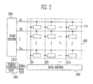
- FIG. 3 illustrates an organic light-emitting display (OLED) according to the present invention. However, it should be understood that an OLED is considered a particular type of an electroluminescent display and should not limit the scope of this invention. Rather, the OLED is being presented as an example of an electroluminescent display for the purposes of illustration and discussion only. Furthermore, the OLED itself is exemplary in nature and the discussion herein should not limit the implementation of such a display, including components utilized, operations performed and connections thereto. Referring to FIG. 3, the OLED has a
pixel unit 100, including a plurality ofpixels 110 connected with scan lines S 1 to Sn and data lines D1 to Dm, adata driving circuit 200 for driving the data lines D1 to Dm, ascan driving circuit 300 for driving the scan lines S1 to Sn, and atiming control unit 400 for controlling thescan driving circuit 300 and thedata driving circuit 200. - The
pixel unit 100 is adapted to receive a first power supply (ELVDD) and a second power supply (ELVSS) from an external source (not illustrated), so as to supply the power to each ofpixels 110. Each of thepixels 110 receiving the first power supply (ELVDD) and the second power supply (ELVSS) can then generate a light corresponding to data signals by controlling a current flowing from the first power supply (ELVDD) to the second power supply (ELVSS) via, for example, a light-emitting diode (not illustrated), that corresponds to the data signals. - The
data driving circuit 200 is adapted to receive data-driving control signals (DCS) from thetiming control unit 400. Thedata driving circuit 200 receiving the data-driving control signals (DCS) can then generate data signals, and supply the generated data signals to data lines D1 to Dm so that they may be synchronized with the scan signals. Thedata driving circuit 200 includes a plurality of switching elements. The switching elements may or may not be all the same type. For example, the switching elements may be realized by PMOS transistors, NMOS transistors or other suitable components, either exclusively, respectively or combinations thereof. - The
scan driving circuit 300 is adapted to receive scan-driving control signals (SCS) from thetiming control unit 400. Thescan driving circuit 300 receiving the scan-driving control signals (SCS) can then generate scan signals and sequentially supply the generated scan signals to scan lines S 1 to Sn. That is, thescan driving circuit 300 can operate to sequentially generate scan signals and supply the generated scan signals to apixel unit 100 which may then drive a plurality of the pixels. - The
timing control unit 400 is adapted to generate data-driving control signals (DCS) and scan-driving control signals (SCS) to correspond to synchronizing signals supplied from an external source (not illustrated). The DCS generated in thetiming control unit 400 are supplied to thedata driving circuit 200 and the SCS are supplied to thescan driving circuit 300. Thetiming control unit 400 may also supply DATA, which may be generated from an external source (not illustrated), to thedata driving circuit 200. - FIG. 4 illustrates a data driving circuit for use with the exemplary OLED illustrated in FIG. 3, according to an embodiment of the present invention. However, it should be understood that this data driving circuit should not be limited to use in the OLED of FIG. 3. Rather, this data driving circuit may be used with other electroluminescent displays.
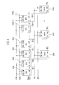
- Referring to FIG. 4, the
data driving circuit 200 includes a shift register and a latch unit. The shift register includes a plurality offirst stages 2101 to 2102n, and each of the first stages can be operated by a first clock (CLK1) and a second clock (CLK2), and then thefirst stage 2101 can output a 1st carrier wave (s[1]) and can transmit the 1st carrier wave (s[1]) to a 2ndfirst stage 2102, Data signals (for example, video data) can be output with the 1st carrier wave (s[1]). The 2ndfirst stage 2102 can receive the 1st carrier wave, and then can transmit the 2nd carrier wave to a 3rd first stage and a 1stsecond stage 2201, and then the 3rd first stage can transmit a 3rd carrier wave to the 4thfirst stage 2104. That is, the even-numberedfirst stages first stage 2103, 2105...2102n-3, 2102n-1) and the second stages. - The latch unit includes a plurality of the
second stages 2201 to 220n, and each of the second stages can be operated by a first enable signal (EN1), a second enable signal (EN2) which can be supplied by first and second enable signal generators. The plurality of thesecond stages 2201 to 220n are connected to output lines of the even-numberedfirst stages first stages second stages 2201 to 220n is half the number of thefirst stages 2101 to 2102n. Also, each of the second stages can simultaneously output the data signals (for example, video data) based on the first enable signal (EN1) and the second enable signal (EN2). Accordingly, the data signals (for example, video data) can be input in series to a plurality of thefirst stages 2101 to 2102n and can be output in parallel by a plurality of thesecond stages 2201 to 220n. - FIG. 5 is a timing diagram illustrating the operation of the data driving circuit shown in FIG. 4. Referring to FIG. 5, the first clock CLK1 is a pulse that is periodically generated and has a longer high period and a shorter low period. The second clock (CLK2) is a similar pulse that is delayed for a predetermined period compared to the first clock (CLK1). The carrier wave (s1) outputs from the 1st
first stage 2101 are generated with the same periodicity as the first clock (CLK1), and the carrier wave (s1) outputs the 1st data (a1) when the signal is at a low level. - The 1st
first stage 2101 receives the input data serially, and continues to sequentially output a n-th data of the 1st data (a1) over the carrier wave (s[1]). In turn, the 2ndfirst stage 2102 receives the 1st carrier wave from the 1stfirst stage 2101, and then outputs the 2nd carrier wave (s2). Therefore, the 2nd carrier wave (s2) outputs the 1st data (a1) after the 1st data (a1) is delayed for a predetermined time compared to the 1st carrier wave (s1), and sequentially outputs the data from the 1st data (a1) to the nth data (an). In this manner, the nth carrier wave (sn) outputs the data from the 1st data (a1) to the nth data (an). The first and second enable signals (EN1, EN2) are input at a point that the 1st data (a1) to nth data (an) are output over the nth carrier wave (sn) of the 1st carrier wave (s1), and then output simultaneously by a plurality of thesecond stages 2201 to 220n. - FIG. 6 illustrates a schematic of another data driving circuit that may be used with the OLED illustrated in FIG. 3, according to an embodiment of the present invention. Again, it should be understood that the data driving circuit should not be limited for use with the OLED of FIG. 3. Rather, this data driving circuit may be used with other electroluminescent displays.
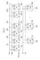
- Referring to FIG. 6, the
data driving circuit 200 includes a shift register and a latch unit. The shift register includes a plurality offirst stages 2101 to 2102n, and each of the first stages is operated by the first clock (CLK1) and the second clock (CLK2). Thefirst stage 2101 outputs the 1st carrier wave (s1) and transmits the 1st carrier wave (s1) to the 2ndfirst stage 2102 and the 1stsecond stage 2201. Data signals (for example, video data) are carried and output in the 1st carrier wave (s1). Thus, the 2ndfirst stage 2102 receives the 1st carrier wave (s1) and transmits the 2nd carrier wave to a 3rdfirst stage 2103, and then the 3rdfirst stage 2103 transmits a 3rd carrier wave (s3) to the 4th first stage and the 2ndsecond stage 2202. That is, the odd-numbered first stages 2001, 2003...2002n-3, 2002n-1 transmit carrier waves to the adjacent first stages (the even-numbered first stage 2002, 2004...2002n-2, 2002n) and the second stages. - The latch unit includes a plurality of the
second stages 2201 to 220n, and each of the second stages is operated by a first enable signal (EN1) and a second enable signal (EN2). The plurality of thesecond stages 2201 to 220n are connected to output lines of the odd-numbered first stages 2001, 2003...2002n-3, 2002n-1 to receive data signals (a1 to an) transmitted from the odd-numbered first stages 2001, 2003...2002n-3, 2002n-1. Accordingly, a plurality of thesecond stages 2201 to 220n have half the number of the plurality of thefirst stages 2101 to 2102n. Also, each of the second stages simultaneously outputs the data signals (for example, video data) based on the first enable signal (EN1) and the second enable signal (EN2). Accordingly, the data signals (for example, video data) are input in series to a plurality of thefirst stages 2101 to 2102n and are output in parallel by a plurality of thesecond stages 2201 to 220n. - FIG. 7 illustrates a timing diagram of an operation of the data driving circuit illustrated in FIG. 6. Referring to FIG. 7, the first clock CLK1 is a pulse that is periodically generated and has a longer high period and a shorter low period. The second clock (CLK2) is a pulse delayed for a predetermined period compared to the first clock (CLK1) pulse. The carrier wave (s1) output from the 1st
first stage 2101 is generated with the same periodicity as the first clock (CLK1), and the carrier wave (s1) outputs data (a1) when the signal is at a low level. The carrier wave (s1) continues to sequentially output a nth data in the 1st data (a1). - The 2nd
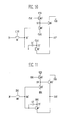
first stage 2102 receives the 1st carrier wave (s1) from the 1st first stage and outputs the 2nd carrier wave (s2). The 2nd carrier wave (s2) outputs the 1st data (a1) after the 1st data (a1) is delayed for a predetermined time as compared to the 1st carrier wave (s[1]), and sequentially outputs the data from the 1st data (a1) to the nth data (an). In this manner, the nthfirst stage 2102n outputs the nth carrier wave (sn). The first and second enable signals (EN1, EN2) are input at a point that the 1st data (a1) to nth data (an) are output over the nth carrier wave (sn) of the 1st carrier wave (s1), and then are simultaneously output by a plurality of thesecond stages 2201 to 220n. - FIG. 8 illustrates a circuit diagram of a first stage that may be used in the data driving circuits illustrated in FIG. 4 and FIG. 6, according to an embodiment of the present invention. FIG. 9 illustrates a circuit diagram of a second stage that may be used in the data driving circuits illustrated in FIG. 4 and FIG. 6, according to an embodiment of the present invention.
- Referring to FIG. 8 and FIG. 9, the first and second stages may have the same configuration, except that the first stage receives a first clock signal (CLK1) and a second clock signal (CLK2), while the second stage receives a first enable signal (EN1) and a second enable signal (EN2). However, although not illustrated, other implementations can be considered where the first and second stages do not have the same configuration. Also, the first stage and the second stage can be realized by PMOS transistors and capacitors. However, other implementations without PMOS transistors and capacitors can be realized.
- Since the first stage and the second stage are connected in the same manner, as discussed above, the first stage and second stage will be described referring to the connection of the first stage only.
- Referring to FIG. 8, in the first transistor (M1), a source is connected to an input terminal (IN), a drain is connected to a first node (N1) and a gate is connected to the second clock (CLK2). In the second transistor (M2), a source is connected to a first clock (CLK1), a drain is connected to a second node (N2), and a gate is connected to the first node (N1). In the third transistor (M3), a source is connected to a third node (N3), a drain is connected to a second power supply (VSS), and a gate is connected to the second clock (CLK2). In the fourth transistor (M4), a source is connected to a second clock (CLK2), a drain is connected to the third node (N3), and a gate is connected to the first node (N1). Also in the fifth transistor (M5), a source is connected to a first power supply (VDD), a drain is connected to an output terminal (OUT), and a gate is connected to the third node (N3). Finally, in a capacitor (C1), a first electrode is connected to the first node (N1), and a second electrode is connected to the second node (N2). The second node (N2) is also connected to the output terminal (OUT). Accordingly, the data signals input through the input terminal (IN) are stored in the capacitor (C1), and then are output through the output terminal (OUT) after a predetermined time.
- FIG. 10 illustrates a circuit diagram of another first stage that may be used in the data driving circuits illustrated in FIG. 4 and FIG. 6. FIG. 11 illustrates a circuit diagram of another second stage. Referring to FIG. 10 and FIG. 11, the first and second stages are realized by NMOS transistors and capacitors. Again, other implementations of the first and second stages can be realized. The first stage is operated after receiving the first clock signal and the second clock signal, and the second stage is operated after receiving the first enable signal and the second enable signal.
- FIG. 12 illustrates a timing diagram of an exemplary operation of the data driving circuit illustrated in FIG. 4, in which the first and second stages illustrated in FIG. 10 and FIG. 11 are used. FIG. 13 illustrates a timing diagram of an exemplary operation of the data driving circuit illustrated in FIG. 6, in which the first and second stages illustrated in FIG. 10 and FIG. 11 are used. Referring to FIG 12 and FIG. 13, waveforms of signals input/output in the first and second stage are realized by NMOS transistors. The signals are reversed, and then input into the first and second stages to operate the data driving circuit, as illustrated in FIG. 6. As a result, a description of FIG. 12 and FIG. 13 is identical to that of FIG. 7.
- As described above, the data driving circuit according to embodiments of the present invention has advantages in that it reduces power consumption by removing paths through which a static current may flow, minimizes a leakage current since the output port is not recharged when a high-level output may be put through the data driving circuit, and also increases an operation rate by minimizing reduction of the current that discharges the output port since the bootstrap is operated when a low-level output is put through the data driving circuit.
- Exemplary embodiments of the present invention have been disclosed herein, and although specific terms are employed, they are used and are to be interpreted in a generic and descriptive sense only and not for purpose of limitation. Accordingly, it will be understood by those of ordinary skill in the art that various changes in form and details may be made without departing from the scope of the present invention as set forth in the following claims.
Claims (15)
- A data driving circuit, comprising:a shift register unit including a plurality of first stages connected in series, the shift register being for receiving data signals and for outputting the data signals, wherein each first stage is arranged to receive the data signals output from a preceding first stage; anda latch unit including a plurality of second stages, wherein each second stage is connected to a different predetermined first stage and is arranged to receive the data signals output from the predetermined first stage, wherein the number of second stages is substantially half the number of the first stages.
- A data driving circuit according to claim 1, wherein the predetermined first stage is an even-numbered one of the plurality of first stages.
- A data driving circuit according to claim 1, wherein the predetermined first stage is an odd-numbered one of the plurality of first stages.
- A data driving circuit as according to any one of claims 1 to 3, wherein each first stage is connected to a first clock and a second clock and is arranged to receive first and second clock signals as inputs, wherein each first stage is arranged to store data signals when the first and the second clock signals are identical to each other and to output the stored data signals when the first and the second clock signals are different from each other.
- A data driving circuit as claimed in claim 4, wherein each first stage comprises:a first transistor connected between an input port and a first node and being arranged to be based on the second clock;a second transistor connected between the first clock and a second node and arranged to be turned on based on a voltage of the first node;a third transistor connected between a third node and a first power supply and arranged to be turned on based on the second clock;a fourth transistor connected between the second clock and a third node and arranged to be turned on based on the voltage of the first node;a fifth transistor connected between a second power supply and an output port and arranged to be turned on based on the voltage of the third node; anda first capacitor connected between the first node and the output port and arranged to maintain the voltages of the output port and the first node.
- A data driving circuit according to claim 5, wherein each of the first stages includes PMOS or NMOS transistors.
- A data driving circuit according to any one of claims 4 to 6, wherein the first and the second clock signals include a data-reading period and a data-transmitting period, and the data-reading period is shorter than the data-transmitting period.
- A data driving circuit according to claim 7, wherein the second clock signal is analogous to a delayed first clock signal.
- A data driving circuit according to any preceding claim, wherein each second stage is arranged to receive a first enable signal and a second enable signal that are input at a same period, wherein each second stage is arranged to store data signals when the first and the second enable signals are identical to each other and to output the stored data signals when the first and the second enable signals are different from each other.
- A data driving circuit according to claim 9, wherein each second stage comprises:a sixth transistor connected between an input port and a fourth node and arranged to be turned on based on the first enable signal generator;a seventh transistor connected between a second enable signal generator and a fifth node and arranged to be turned on based on a voltage of the fourth node;an eighth transistor connected between a first power supply and a sixth node and arranged to be turned on based on the first enable signal generator;a ninth transistor connected between the first enable signal generator and the sixth node and arranged to be turned on based on the voltage of the fourth node;a tenth transistor connected between a second power supply and an output port and arranged to be turned on based on a voltage of the sixth node; anda second capacitor connected between the fourth node and the output port, the second capacitor being arranged to maintain the voltages of the output port and the fourth node.
- A data driving circuit according to claim 10, wherein each of the second stages includes PMOS or NMOS transistors.
- A data driving circuit according to any one of claims 9 to 11, wherein the second stages are arranged to output simultaneously the data signals in parallel based on the first and the second enable signals.
- A data driving circuit according to claim 12, wherein the first and the second enable signals have waveforms of the first and the second clock signals at an applied point.
- A data driving circuit according to any preceding claim, including a D/A converter connected to the latch unit, wherein the D/A converter receives digital data signals from the latch unit and outputs analog data signals.
- An electroluminescent display, comprising:a pixel unit including pixels for receiving data signals and scan signals;a scan driving circuit for transmitting the data signals to the pixels; anda data driving circuit according to any one of claims 1 to 14 for transmitting the scan signals to the pixels,
Applications Claiming Priority (1)
| Application Number | Priority Date | Filing Date | Title |
|---|---|---|---|
| KR1020050106171A KR100762690B1 (en) | 2005-11-07 | 2005-11-07 | scan driving circuit and Organic Light Emitting Display Using the same |
Publications (3)
| Publication Number | Publication Date |
|---|---|
| EP1783739A2 true EP1783739A2 (en) | 2007-05-09 |
| EP1783739A3 EP1783739A3 (en) | 2008-12-24 |
| EP1783739B1 EP1783739B1 (en) | 2013-09-11 |
Family
ID=37602957
Family Applications (1)
| Application Number | Title | Priority Date | Filing Date |
|---|---|---|---|
| EP06255725.1A Expired - Fee Related EP1783739B1 (en) | 2005-11-07 | 2006-11-07 | Data driving circuit and electroluminescent display using the same |
Country Status (5)
| Country | Link |
|---|---|
| US (1) | US7982704B2 (en) |
| EP (1) | EP1783739B1 (en) |
| JP (1) | JP5150812B2 (en) |
| KR (1) | KR100762690B1 (en) |
| CN (1) | CN100565640C (en) |
Cited By (1)
| Publication number | Priority date | Publication date | Assignee | Title |
|---|---|---|---|---|
| US7982704B2 (en) | 2005-11-07 | 2011-07-19 | Samsung Mobile Display Co., Ltd. | Data driving circuit and electroluminescent display using the same |
Families Citing this family (19)
| Publication number | Priority date | Publication date | Assignee | Title |
|---|---|---|---|---|
| KR101352114B1 (en) * | 2007-07-04 | 2014-01-14 | 엘지디스플레이 주식회사 | Flat Panel Display Device |
| JP2009211732A (en) * | 2008-02-29 | 2009-09-17 | Eastman Kodak Co | Shift register circuit and display |
| KR100941843B1 (en) * | 2008-04-14 | 2010-02-11 | 삼성모바일디스플레이주식회사 | Inverter and display device having the same |
| TWI406234B (en) * | 2008-05-07 | 2013-08-21 | Au Optronics Corp | Lcd device based on dual source drivers with data writing synchronous control mechanism and related driving method |
| KR101721639B1 (en) | 2010-10-28 | 2017-03-31 | 삼성디스플레이 주식회사 | Driver, display device comprising the same |
| KR101881853B1 (en) * | 2012-02-29 | 2018-07-26 | 삼성디스플레이 주식회사 | Emission driving unit, emission driver and organic light emitting display device having the same |
| CN102682692B (en) * | 2012-05-21 | 2014-11-05 | 京东方科技集团股份有限公司 | Shift register, drive device and displayer |
| US9171514B2 (en) * | 2012-09-03 | 2015-10-27 | Samsung Electronics Co., Ltd. | Source driver, method thereof, and apparatuses having the same |
| CN103151010B (en) * | 2013-02-27 | 2014-12-10 | 京东方科技集团股份有限公司 | Shift register and display device |
| CN103198866B (en) * | 2013-03-06 | 2015-08-05 | 京东方科技集团股份有限公司 | Shift register, gate driver circuit, array base palte and display device |
| CN104751769A (en) * | 2013-12-25 | 2015-07-01 | 昆山工研院新型平板显示技术中心有限公司 | Scanning driver and organic light emitting display employing same |
| TWI520117B (en) * | 2014-02-07 | 2016-02-01 | 友達光電股份有限公司 | Shift control cell |
| CN104157252B (en) * | 2014-07-29 | 2017-01-18 | 京东方科技集团股份有限公司 | Shifting register, gate driving circuit and display device |
| CN104167175B (en) * | 2014-08-06 | 2016-08-31 | 上海和辉光电有限公司 | Oled |
| CN104751816B (en) * | 2015-03-31 | 2017-08-15 | 深圳市华星光电技术有限公司 | Shift-register circuit |
| CN105185411B (en) * | 2015-06-30 | 2019-03-26 | 上海天马有机发光显示技术有限公司 | A kind of shift register and its driving method |
| JP6539567B2 (en) * | 2015-10-30 | 2019-07-03 | 株式会社ジャパンディスプレイ | Display device |
| CN105957556A (en) * | 2016-05-11 | 2016-09-21 | 京东方科技集团股份有限公司 | Shift register unit, gate drive circuit, display apparatus, and driving method of shift register unit |
| CN107103870A (en) * | 2017-06-27 | 2017-08-29 | 上海天马有机发光显示技术有限公司 | Shifting deposit unit, its driving method and display panel |
Citations (2)
| Publication number | Priority date | Publication date | Assignee | Title |
|---|---|---|---|---|
| US6339631B1 (en) * | 1999-03-02 | 2002-01-15 | Lg. Philips Lcd Co., Ltd. | Shift register |
| US6784864B1 (en) * | 1999-07-12 | 2004-08-31 | Semiconductor Energy Laboratory Co., Ltd. | Digital driver and display device |
Family Cites Families (12)
| Publication number | Priority date | Publication date | Assignee | Title |
|---|---|---|---|---|
| JP3713401B2 (en) * | 1999-03-18 | 2005-11-09 | 株式会社東芝 | Charge pump circuit |
| JP2001083923A (en) * | 1999-07-12 | 2001-03-30 | Semiconductor Energy Lab Co Ltd | Digital driver and display device |
| KR100563826B1 (en) * | 1999-08-21 | 2006-04-17 | 엘지.필립스 엘시디 주식회사 | Data driving circuit of liquid crystal display |
| JP2004153444A (en) * | 2002-10-29 | 2004-05-27 | Renesas Technology Corp | Chopper type comparator |
| KR100700177B1 (en) * | 2002-12-18 | 2007-03-27 | 엘지.필립스 엘시디 주식회사 | Low power driving method of electro-luminescence display |
| JP2005235311A (en) * | 2004-02-19 | 2005-09-02 | Olympus Corp | Signal transmission circuit |
| KR101030528B1 (en) * | 2004-05-27 | 2011-04-26 | 엘지디스플레이 주식회사 | The shift resistor and the liquid crystal display device using the same |
| KR100729099B1 (en) * | 2005-09-20 | 2007-06-14 | 삼성에스디아이 주식회사 | scan driving circuit and Organic Light Emitting Display Using the same |
| KR100658284B1 (en) * | 2005-09-30 | 2006-12-14 | 삼성에스디아이 주식회사 | Scan driving circuit and organic light emitting display using the same |
| KR100762690B1 (en) | 2005-11-07 | 2007-10-01 | 삼성에스디아이 주식회사 | scan driving circuit and Organic Light Emitting Display Using the same |
| KR100719670B1 (en) * | 2006-04-06 | 2007-05-18 | 삼성에스디아이 주식회사 | Data driver and organic light emitting display using the same |
| KR100748321B1 (en) * | 2006-04-06 | 2007-08-09 | 삼성에스디아이 주식회사 | Scan driving circuit and organic light emitting display using the same |
-
2005
- 2005-11-07 KR KR1020050106171A patent/KR100762690B1/en not_active IP Right Cessation
-
2006
- 2006-06-07 JP JP2006158771A patent/JP5150812B2/en not_active Expired - Fee Related
- 2006-11-06 US US11/593,006 patent/US7982704B2/en not_active Expired - Fee Related
- 2006-11-07 CN CNB2006100644199A patent/CN100565640C/en not_active Expired - Fee Related
- 2006-11-07 EP EP06255725.1A patent/EP1783739B1/en not_active Expired - Fee Related
Patent Citations (2)
| Publication number | Priority date | Publication date | Assignee | Title |
|---|---|---|---|---|
| US6339631B1 (en) * | 1999-03-02 | 2002-01-15 | Lg. Philips Lcd Co., Ltd. | Shift register |
| US6784864B1 (en) * | 1999-07-12 | 2004-08-31 | Semiconductor Energy Laboratory Co., Ltd. | Digital driver and display device |
Cited By (1)
| Publication number | Priority date | Publication date | Assignee | Title |
|---|---|---|---|---|
| US7982704B2 (en) | 2005-11-07 | 2011-07-19 | Samsung Mobile Display Co., Ltd. | Data driving circuit and electroluminescent display using the same |
Also Published As
| Publication number | Publication date |
|---|---|
| JP5150812B2 (en) | 2013-02-27 |
| CN101013556A (en) | 2007-08-08 |
| CN100565640C (en) | 2009-12-02 |
| EP1783739B1 (en) | 2013-09-11 |
| EP1783739A3 (en) | 2008-12-24 |
| KR20070049005A (en) | 2007-05-10 |
| US7982704B2 (en) | 2011-07-19 |
| KR100762690B1 (en) | 2007-10-01 |
| JP2007133358A (en) | 2007-05-31 |
| US20070103389A1 (en) | 2007-05-10 |
Similar Documents
| Publication | Publication Date | Title |
|---|---|---|
| EP1783739B1 (en) | Data driving circuit and electroluminescent display using the same | |
| KR100776511B1 (en) | Scan driving circuit and organic light emitting display using the same | |
| CN110176217B (en) | Shifting register unit and driving method thereof, grid driving circuit and display device | |
| KR100729099B1 (en) | scan driving circuit and Organic Light Emitting Display Using the same | |
| KR100658269B1 (en) | Scan driving circuit and organic light emitting display using the same | |
| CN108597438B (en) | Shifting register unit, grid driving circuit and driving method thereof and display device | |
| US7663593B2 (en) | Level shift circuit and shift register and display device | |
| US7639217B2 (en) | Scan driving circuit and organic light emitting display device using the same | |
| CN114495829B (en) | Shifting register unit, driving method, grid driving circuit and display device | |
| US7656194B2 (en) | Shift register circuit | |
| US8836631B2 (en) | Scan driving circuit with a shift register and electroluminescent display using the same | |
| US11798482B2 (en) | Gate driver and organic light emitting display device including the same | |
| EP1848000B1 (en) | Scan driving circuit and organic light emitting display using the same | |
| KR100658270B1 (en) | Scan driving circuit and organic light emitting display using the same | |
| KR100662983B1 (en) | Scan driving circuit and organic light emitting display using the same |
Legal Events
| Date | Code | Title | Description |
|---|---|---|---|
| PUAI | Public reference made under article 153(3) epc to a published international application that has entered the european phase |
Free format text: ORIGINAL CODE: 0009012 |
|
| 17P | Request for examination filed |
Effective date: 20061110 |
|
| AK | Designated contracting states |
Kind code of ref document: A2 Designated state(s): AT BE BG CH CY CZ DE DK EE ES FI FR GB GR HU IE IS IT LI LT LU LV MC NL PL PT RO SE SI SK TR |
|
| AX | Request for extension of the european patent |
Extension state: AL BA HR MK YU |
|
| PUAL | Search report despatched |
Free format text: ORIGINAL CODE: 0009013 |
|
| AK | Designated contracting states |
Kind code of ref document: A3 Designated state(s): AT BE BG CH CY CZ DE DK EE ES FI FR GB GR HU IE IS IT LI LT LU LV MC NL PL PT RO SE SI SK TR |
|
| AX | Request for extension of the european patent |
Extension state: AL BA HR MK RS |
|
| RAP1 | Party data changed (applicant data changed or rights of an application transferred) |
Owner name: SAMSUNG MOBILE DISPLAY CO., LTD. |
|
| AKX | Designation fees paid |
Designated state(s): DE FR GB |
|
| 17Q | First examination report despatched |
Effective date: 20091012 |
|
| GRAP | Despatch of communication of intention to grant a patent |
Free format text: ORIGINAL CODE: EPIDOSNIGR1 |
|
| RAP1 | Party data changed (applicant data changed or rights of an application transferred) |
Owner name: SAMSUNG DISPLAY CO., LTD. |
|
| GRAP | Despatch of communication of intention to grant a patent |
Free format text: ORIGINAL CODE: EPIDOSNIGR1 |
|
| INTG | Intention to grant announced |
Effective date: 20130703 |
|
| GRAS | Grant fee paid |
Free format text: ORIGINAL CODE: EPIDOSNIGR3 |
|
| GRAA | (expected) grant |
Free format text: ORIGINAL CODE: 0009210 |
|
| AK | Designated contracting states |
Kind code of ref document: B1 Designated state(s): DE FR GB |
|
| REG | Reference to a national code |
Ref country code: GB Ref legal event code: FG4D |
|
| REG | Reference to a national code |
Ref country code: DE Ref legal event code: R096 Ref document number: 602006038334 Country of ref document: DE Effective date: 20131107 |
|
| REG | Reference to a national code |
Ref country code: DE Ref legal event code: R097 Ref document number: 602006038334 Country of ref document: DE |
|
| PLBE | No opposition filed within time limit |
Free format text: ORIGINAL CODE: 0009261 |
|
| STAA | Information on the status of an ep patent application or granted ep patent |
Free format text: STATUS: NO OPPOSITION FILED WITHIN TIME LIMIT |
|
| 26N | No opposition filed |
Effective date: 20140612 |
|
| REG | Reference to a national code |
Ref country code: DE Ref legal event code: R097 Ref document number: 602006038334 Country of ref document: DE Effective date: 20140612 |
|
| REG | Reference to a national code |
Ref country code: FR Ref legal event code: PLFP Year of fee payment: 10 |
|
| PGFP | Annual fee paid to national office [announced via postgrant information from national office to epo] |
Ref country code: GB Payment date: 20151026 Year of fee payment: 10 Ref country code: DE Payment date: 20151028 Year of fee payment: 10 |
|
| PGFP | Annual fee paid to national office [announced via postgrant information from national office to epo] |
Ref country code: FR Payment date: 20151026 Year of fee payment: 10 |
|
| REG | Reference to a national code |
Ref country code: DE Ref legal event code: R119 Ref document number: 602006038334 Country of ref document: DE |
|
| GBPC | Gb: european patent ceased through non-payment of renewal fee |
Effective date: 20161107 |
|
| REG | Reference to a national code |
Ref country code: FR Ref legal event code: ST Effective date: 20170731 |
|
| PG25 | Lapsed in a contracting state [announced via postgrant information from national office to epo] |
Ref country code: FR Free format text: LAPSE BECAUSE OF NON-PAYMENT OF DUE FEES Effective date: 20161130 |
|
| PG25 | Lapsed in a contracting state [announced via postgrant information from national office to epo] |
Ref country code: GB Free format text: LAPSE BECAUSE OF NON-PAYMENT OF DUE FEES Effective date: 20161107 Ref country code: DE Free format text: LAPSE BECAUSE OF NON-PAYMENT OF DUE FEES Effective date: 20170601 |