EP1780787A2 - Joining structure between ceramic substrate and power supply connector - Google Patents
Joining structure between ceramic substrate and power supply connector Download PDFInfo
- Publication number
- EP1780787A2 EP1780787A2 EP06255533A EP06255533A EP1780787A2 EP 1780787 A2 EP1780787 A2 EP 1780787A2 EP 06255533 A EP06255533 A EP 06255533A EP 06255533 A EP06255533 A EP 06255533A EP 1780787 A2 EP1780787 A2 EP 1780787A2
- Authority
- EP
- European Patent Office
- Prior art keywords
- stress relaxation
- insert member
- counterbore
- relaxation insert
- protrusion
- Prior art date
- Legal status (The legal status is an assumption and is not a legal conclusion. Google has not performed a legal analysis and makes no representation as to the accuracy of the status listed.)
- Granted
Links
Images



Classifications
-
- H—ELECTRICITY
- H10—SEMICONDUCTOR DEVICES; ELECTRIC SOLID-STATE DEVICES NOT OTHERWISE PROVIDED FOR
- H10P—GENERIC PROCESSES OR APPARATUS FOR THE MANUFACTURE OR TREATMENT OF DEVICES COVERED BY CLASS H10
- H10P72/00—Handling or holding of wafers, substrates or devices during manufacture or treatment thereof
- H10P72/50—Handling or holding of wafers, substrates or devices during manufacture or treatment thereof for positioning, orientation or alignment
-
- H—ELECTRICITY
- H10—SEMICONDUCTOR DEVICES; ELECTRIC SOLID-STATE DEVICES NOT OTHERWISE PROVIDED FOR
- H10P—GENERIC PROCESSES OR APPARATUS FOR THE MANUFACTURE OR TREATMENT OF DEVICES COVERED BY CLASS H10
- H10P72/00—Handling or holding of wafers, substrates or devices during manufacture or treatment thereof
- H10P72/70—Handling or holding of wafers, substrates or devices during manufacture or treatment thereof for supporting or gripping
- H10P72/72—Handling or holding of wafers, substrates or devices during manufacture or treatment thereof for supporting or gripping using electrostatic chucks
-
- H—ELECTRICITY
- H02—GENERATION; CONVERSION OR DISTRIBUTION OF ELECTRIC POWER
- H02N—ELECTRIC MACHINES NOT OTHERWISE PROVIDED FOR
- H02N13/00—Clutches or holding devices using electrostatic attraction, e.g. using Johnson-Rahbek effect
Definitions
- the present invention relates to a structure with which to join a ceramic substrate having a metal member buried therein and a power supply connector for supplying power to the metal member (the structure is hereinafter referred to as a "joining structure between the ceramic substrate and the power supply connector.")
- the device has heretofore been put to practical use, which generates high-frequency power and heats a ceramic substrate such as aluminum nitride by electrically connecting a power supply connector to a metal member, such as a metal electrode or a metal resistor, which is buried in the ceramic substrate and thus supplying power to the metal member from the power supply connector.
- a metal member such as a metal electrode or a metal resistor
- an opening is formed in the ceramic substrate so as to expose at least a part of the metal member, and the metal member and the power supply connector are directly joined to each other in a bottom portion of the opening.
- the device has a structure in which the metal member and the power supply connector are joined to each other in the bottom portion of the opening as described above.
- strength of a joining part against bending stress is low, and the power supply connector is likely to be disjoined from the metal member by a bending load from the outside.
- oxygen entering from the opening deteriorates the joining part, particularly, the metal member. Accordingly, life of the joining part (electrically connected) is shortened.
- the present invention was made in consideration of the foregoing demand. It is an object of the present invention toprovide a joining structure between a ceramic substrate and a power supply connector, which can maintain high joining strength and good electrical connection for a long time.
- a joining structure between a ceramic substrate in which a metal member is buried and a power supply connector which supplies power to the metal member according to the present invention includes; a counterbore formed in the ceramic substrate so as to have a large-diameter part and a small-diameter part formed at the bottom center of the large-diameter part, at least a part of the metal member is exposed from the bottom of the small-diameter part; a stress relaxation insert member having a body part and a protrusion and being provided in the counterbore in a state where the body part and the protrusion are fitted into the large-diameter part and the small-diameter part, respectively; and a brazing member, which connects the power supply connector to the stress relaxation insert member, and which seals a gap between the counterbore and the stress relaxation insert member.
- the present invention is applicable to a high-frequency generation electrode device which generates high-frequency power by electrically connecting a power supply connector to RF (Radio Frequency) electrodes buried in a ceramic substrate so as to supply power to the RF electrodes through the power supply connector.
- RF Radio Frequency
- the present invention is applicable as long as the device has a joining structure between a metal member buried in a ceramic substrate and a power supply connector, such as a heater having a resistor buried in a ceramic substrate, an electrostatic chuck havingan electrostatic chuck electrodeburied ina ceramic substrate, a heater with an electrostatic chuck having a heating resistor and an electrostatic chuck electrode buried in a ceramic substrate, and a high-frequency generation electrode device with a heater having RF electrodes and a heating resistor buried in a ceramic substrate.
- a high-frequency generation electrode device 1 of the embodiment of the present invention includes: a roughly disk-shaped ceramic substrate 2 made of AlN (aluminum nitride); and RF electrodes 3 which are buried in the ceramic substrate 2 and made of a Mo (molybdenum) mesh.
- a counterbore 4 is formed in the ceramic substrate 2 so as to expose a part of the RF electrodes 3.
- a stress relaxation insert member 5 made of Kovar or Permalloy is provided in such a manner that a protrusion 5a thereof having a shape that fits into a shape of a small-diameter hole of the counterbore 4 is inserted.
- a space between the counterbore 4 and the stress relaxation insert member 5 is sealed by a brazing member 6 made of a metal material containing at least Au such as Au (gold) -Ni (nickel) solder or A1 (aluminum) .
- the stress relaxation insert member 5 is hermetically joined to a feeder rod 8 made of Ni by the brazing member 6 and an atmosphere protecting tube 7.
- the high-frequency generation electrode device 1 having the configuration as described above generates high-frequency power as power supplied to the feeder rod 8 is supplied to the RF electrodes 3 through the stress relaxation insert member 5 and the brazing member 6.
- an active metal foil 9 containing at least one of Ti (titanium), Zr (zirconium) and Hf (hafnium) may be provided between the RF electrodes 3 and the brazing member 6.
- the high-frequency generation electrode device 1 In manufacturing of the high-frequency generation electrode device 1, first, after AlN raw powder is turned into granulated powder by a spray dryer, RF electrodes 3 are buried in the granulated powder and uniaxial press molding is performed thereon. Thereafter, a molded body obtained is subjected to hot press firing in a nitrogen atmosphere at a temperature of 1900 [°C] and a pressure of 100 [kg/cm 2 ]. Thus, a roughly disk-shaped ceramic substrate 2 having a configuration as shown in Fig. 3A is fabricated. Note that, the ceramic substrate 2 is fabricated so as to have a diameter of 330 [mm] and a thickness of 15 [mm], in this embodiment.
- the ceramic substrate 2 shown in Fig. 3A holes such as a lift pin hole (not shown), a terminal hole (not shown) and a counterbore 4 are processed.
- the substrate is subjected to finish processing for its external shape and to cleaning.
- the ceramic substrate 2 having a configuration as shown in Fig. 3B is fabricated.
- the shaft described above is fabricated to have a diameter of 55 [mm] and a wall thickness of 3 [mm]
- the terminal hole is fabricated to have a diameter of 7 [mm] and a depth of 14 [mm].
- the counterbore 4 is fabricated so as to appropriately correspond to a shape of a stress relaxation insert member 5 .
- the counterbore 4 is fabricated in such a manner that, when the stress relaxation insert member 5 is provided, a side clearance on one side between the counterbore 4 and the stress relaxation insert member 5 is set at 0.2 [mm].
- an atmosphere protecting tube 7 is provided in a large-diameter bottom portion of the counterbore 4 in the ceramic substrate 2 shown in Fig. 3B.
- a brazing member 6 made of Au alloy the stress relaxation insert member 5 and the feeder rod 8 are sequentially set inside the atmosphere protecting tube 7, a brazing member 6 made of Au alloy, the stress relaxation insert member 5 and the feeder rod 8 are sequentially set. Thereafter, the stress relaxation insert member 5 and the feeder rod 8 are hermetically joined to each other by heating to about 1000 [°C] at a vacuum of 1E-3 [Pa] in a vacuum furnace.
- a heating temperature is set at about 600 [°C].
- the stress relaxation insert member 5 should be formed so as for b/a to take on a value in a range of 0.3 to 0.8, where a denotes the horizontal length of a plane of the stress relaxation insert member 5 on which a protrusion 5a is formed, and b denotes the horizontal length of the protrusion 5a.
- a denotes the horizontal length of a plane of the stress relaxation insert member 5 on which a protrusion 5a is formed
- b denotes the horizontal length of the protrusion 5a.
- the stress relaxation insert member 5 is formed so as to set a value of c/b within a range of 0.05 to 2.0. This is because, when the value of c/b is 0.05 or less, a joining area of the protrusion 5a with a side part of the ceramic substrate 2 is reduced, which does not contribute to improvement in the joining strength of the joining part. Moreover, when the value of c/b is 2.0 or more, a side distance of the joining part is too long and thus residual stress is increased. Therefore, the ceramic substrate 2 is likely to be damaged.
- the Fig. 5 shows results obtained by respectively performing conduction cycle tests on high-frequency generation electrode devices provided with stress relaxation insert members having dimensions of examples 1 to 6, high-frequency generation electrode devices provided with stress relaxation insert members having dimensions of comparative examples 1 to 4, and a conventional high-frequency generation electrode device (without a stress relaxation insert member).
- a cycle of heating the device from 100 [°C] to 700 [°C] at a heating rate of 10 ['C / min] and, thereafter, cooling the device from 700 [°C] to 100 [°C] at an average cooling rate of 7 [°C /min] in a state where power is being distributed to a RF electrodes is repeated.
- a Kovar material is used as the stress relaxation insert member
- Au alloy is used as a brazing member.
- no active metal foil 9 is provided between the RF electrodes and the brazing member.
- the joining strength means a 30A [gf ⁇ cm] of bending moment when the bending moment is applied to the joining part by applying a load A to a tip portion of the 30- [cm] feeder rod in a direction perpendicular to an axial direction of the feeder rod and the joining part is damaged.
- the stress relaxation insert member 5 has a horizontal length a and the protrusion 5a has a horizontal length b and a height c
- the stress relaxation insert member 5 is formed so as to set a value of b/a within a range of 0.3 to 0.8 and a value of c/b within a range of 0.05 to 2.0.
- the Fig. 6 shows results obtained by performing conduction cycle tests similar to those described above on the high-frequency generation electrode device provided with the stress relaxation insert member having the dimensions of example 1 shown in Table 1. Specifically, the conduction cycle tests are carried out by providing various active metal foils between the RF electrodes and the brazing member of the high-frequency generation electrode device.
- the Fig. 7 shows results obtained by performing conduction cycle tests respectively on the high- frequency generation electrode devices provided with the stress relaxation insert members having the dimensions of examples shown in Table 1 and the conventional high-frequency generation electrode device (without a stress relaxation insert member), by changing materials of the stress relaxation insert member and the brazing member.
- a cycle of heating the device from 100 [°C] to 500 [°C] at a heating rate of 10 ['C / min] in a state where power is being distributed to the RF electrodes and, thereafter, cooling the device from 500 [°C] to 100 [°C] at an average cooling rate of 7 [°C/ min] is repeated.
- the metal member and the power supply connector are joined to each other by use of the stress relaxation insert member provided in the counterbore and the brazing member that seals the entire counterbore.
- a joining part thereof is substantially joined to also a side part of the ceramic substrate. Consequently, strength against bending stress can be improved.
- the entire joining part between the ceramic substrate and the power supply connector is sealed by the brazing member. Therefore, a rate of oxygen entering the joining part is lowered. Thus, life of the joining part can be extended.
Landscapes
- Ceramic Products (AREA)
- Container, Conveyance, Adherence, Positioning, Of Wafer (AREA)
- Connection Of Plates (AREA)
Abstract
Description
- This application is based upon and claims the benefit of priority from a
Japanese Patent Application No. TOKUGAN 2005-314603, filed on October 28, 2005 - The present invention relates to a structure with which to join a ceramic substrate having a metal member buried therein and a power supply connector for supplying power to the metal member (the structure is hereinafter referred to as a "joining structure between the ceramic substrate and the power supply connector.")
- The device has heretofore been put to practical use, which generates high-frequency power and heats a ceramic substrate such as aluminum nitride by electrically connecting a power supply connector to a metal member, such as a metal electrode or a metal resistor, which is buried in the ceramic substrate and thus supplying power to the metal member from the power supply connector. In such a device, as disclosed in
Japanese Patent Laid-Open No. Hei 10 (1998) -209255 Japanese Patent Laid-Open No. Hei 11 (1999) -12053 Japanese Patent Publication No. 3681824 - The device has a structure in which the metal member and the power supply connector are joined to each other in the bottom portion of the opening as described above. Thus, strength of a joining part against bending stress is low, and the power supply connector is likely to be disjoined from the metal member by a bending load from the outside. Moreover, oxygen entering from the opening deteriorates the joining part, particularly, the metal member. Accordingly, life of the joining part (electrically connected) is shortened. Against such a background, there is an urgent market need to provide a joining structure between a metal member and a power supply connector, which can maintain higher joining strength and good electrical connection for a long time.
- The present invention was made in consideration of the foregoing demand. It is an object of the present invention toprovide a joining structure between a ceramic substrate and a power supply connector, which can maintain high joining strength and good electrical connection for a long time.
- In order to solve the problems described above, a joining structure between a ceramic substrate in which a metal member is buried and a power supply connector which supplies power to the metal member according to the present invention includes; a counterbore formed in the ceramic substrate so as to have a large-diameter part and a small-diameter part formed at the bottom center of the large-diameter part, at least a part of the metal member is exposed from the bottom of the small-diameter part; a stress relaxation insert member having a body part and a protrusion and being provided in the counterbore in a state where the body part and the protrusion are fitted into the large-diameter part and the small-diameter part, respectively; and a brazing member, which connects the power supply connector to the stress relaxation insert member, and which seals a gap between the counterbore and the stress relaxation insert member.
-
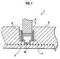
- Fig. 1 is a cross-sectional view showing a configuration of a high-frequency generation electrode device of an embodiment of the present invention;
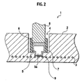
- Fig. 2 is a cross-sectional view showing a configuration of an application example of the high-frequency generation electrode device shown in Fig. 1;
- Figs. 3A to 3C are cross-sectional views showing stages of a method of manufacturing the high-frequency generation electrode device of the embodiment of the present invention;
- Fig. 4 is a schematic view for explaining dimensions of a stress relaxation insert member shown in Fig. 1;
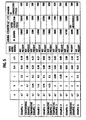
- Fig. 5 is a table showing results obtained by performing thermal cycle tests on high-frequency generation electrode devices provided with stress relaxation insert members having dimensions of examples 1 to 6, comparative examples 1 to 4, and a conventional high-frequency generation electrode device;
- Fig. 6 is a table showing results obtained by performing conduction cycle tests on the high-frequency generation electrode device having the dimensions of example 1 shown in Fig. 5; and
- Fig. 7 is a table showing results obtained by performing conduction cycle tests on the high-frequency generation electrode devices provided with the stress relaxation insert members having the dimensions of examples shown in Fig. 5 and the conventional high-frequency generation electrode device.
- Detailed description of preferred embodiments of the present invention will be given below by referring to the accompanying drawings. It should be noted that the same reference numerals are used in the following drawings among the components having same function, and the same description is not repeated.
- The present invention is applicable to a high-frequency generation electrode device which generates high-frequency power by electrically connecting a power supply connector to RF (Radio Frequency) electrodes buried in a ceramic substrate so as to supply power to the RF electrodes through the power supply connector. With reference to the drawings, detailed description will be given below of a configuration of a high-frequency generation electrode device of an embodiment of the present invention and a manufacturing method thereof. Note that application of the present invention is not limited to the high-frequency generation electrode device described above. The present invention is applicable as long as the device has a joining structure between a metal member buried in a ceramic substrate and a power supply connector, such as a heater having a resistor buried in a ceramic substrate, an electrostatic chuck havingan electrostatic chuck electrodeburied ina ceramic substrate, a heater with an electrostatic chuck having a heating resistor and an electrostatic chuck electrode buried in a ceramic substrate, and a high-frequency generation electrode device with a heater having RF electrodes and a heating resistor buried in a ceramic substrate. [Configuration of High-Frequency Generation Electrode Device]
- First, with reference to Fig. 1, description will be given of a configuration of a high-frequency generation electrode device to be an embodiment of the present invention.
- As shown in Fig. 1, a high-frequency
generation electrode device 1 of the embodiment of the present invention includes: a roughly disk-shapedceramic substrate 2 made of AlN (aluminum nitride); andRF electrodes 3 which are buried in theceramic substrate 2 and made of a Mo (molybdenum) mesh. Acounterbore 4 is formed in theceramic substrate 2 so as to expose a part of theRF electrodes 3. In thecounterbore 4, a stress relaxation insertmember 5 made of Kovar or Permalloy is provided in such a manner that aprotrusion 5a thereof having a shape that fits into a shape of a small-diameter hole of thecounterbore 4 is inserted. A space between thecounterbore 4 and the stressrelaxation insert member 5 is sealed by a brazingmember 6 made of a metal material containing at least Au such as Au (gold) -Ni (nickel) solder or A1 (aluminum) . The stressrelaxation insert member 5 is hermetically joined to a feeder rod 8 made of Ni by thebrazing member 6 and anatmosphere protecting tube 7. - The high-frequency
generation electrode device 1 having the configuration as described above generates high-frequency power as power supplied to the feeder rod 8 is supplied to theRF electrodes 3 through the stress relaxation insertmember 5 and the brazingmember 6. Note that, as a configuration of an application of the high-frequencygeneration electrode device 1, as shown in Fig. 2, an active metal foil 9 containing at least one of Ti (titanium), Zr (zirconium) and Hf (hafnium) may be provided between theRF electrodes 3 and the brazingmember 6. By use of the configuration as described above, joining strength between theRF electrodes 3 and the brazingmember 6 can be further improved. - Next, with reference to Figs. 3A to 3C, description will be given of a method for manufacturing the high-frequency
generation electrode device 1 described above. - In manufacturing of the high-frequency
generation electrode device 1, first, after AlN raw powder is turned into granulated powder by a spray dryer,RF electrodes 3 are buried in the granulated powder and uniaxial press molding is performed thereon. Thereafter, a molded body obtained is subjected to hot press firing in a nitrogen atmosphere at a temperature of 1900 [°C] and a pressure of 100 [kg/cm2]. Thus, a roughly disk-shapedceramic substrate 2 having a configuration as shown in Fig. 3A is fabricated. Note that, theceramic substrate 2 is fabricated so as to have a diameter of 330 [mm] and a thickness of 15 [mm], in this embodiment. - Next, in the
ceramic substrate 2 shown in Fig. 3A, holes such as a lift pin hole (not shown), a terminal hole (not shown) and acounterbore 4 are processed. At the same time, a shaft (not shown) made of A1N, in which a hole for passing a feeder rod 8 is formed, is solid-phase welded. Thereafter, the substrate is subjected to finish processing for its external shape and to cleaning. Thus, theceramic substrate 2 having a configuration as shown in Fig. 3B is fabricated. Note that the shaft described above is fabricated to have a diameter of 55 [mm] and a wall thickness of 3 [mm], and the terminal hole is fabricated to have a diameter of 7 [mm] and a depth of 14 [mm]. Moreover, in this embodiment, thecounterbore 4 is fabricated so as to appropriately correspond to a shape of a stressrelaxation insert member 5 . Specifically, thecounterbore 4 is fabricated in such a manner that, when the stressrelaxation insert member 5 is provided, a side clearance on one side between thecounterbore 4 and the stressrelaxation insert member 5 is set at 0.2 [mm]. - Next, an
atmosphere protecting tube 7 is provided in a large-diameter bottom portion of thecounterbore 4 in theceramic substrate 2 shown in Fig. 3B. Moreover, inside theatmosphere protecting tube 7, a brazingmember 6 made of Au alloy, the stress relaxation insertmember 5 and the feeder rod 8 are sequentially set. Thereafter, the stress relaxation insertmember 5 and the feeder rod 8 are hermetically joined to each other by heating to about 1000 [°C] at a vacuum of 1E-3 [Pa] in a vacuum furnace. Note that, when thebrazing member 6 is made of Al or Al-Mg alloy, a heating temperature is set at about 600 [°C]. By the series of stages described above, the high-frequencygeneration electrode device 1 is manufactured. - Note that, it is desirable that the stress
relaxation insert member 5 should be formed so as for b/a to take on a value in a range of 0.3 to 0.8, where a denotes the horizontal length of a plane of the stressrelaxation insert member 5 on which aprotrusion 5a is formed, and b denotes the horizontal length of theprotrusion 5a. This is because, when the value of b/a is 0.3 or less, a joining area with theRF electrodes 3 is reduced, which does not contribute to improvement in joining strength of a joining part. Moreover, when the value of b/a is 0.8 or more, an exposed area of theRF electrodes 3 is increased too much and thus oxygen easily enters into the joining part. Therefore, life of the joining part is not improved. - As shown in Fig. 4, assuming that the
protrusion 5a has a height c, it is preferable that the stressrelaxation insert member 5 is formed so as to set a value of c/b within a range of 0.05 to 2.0. This is because, when the value of c/b is 0.05 or less, a joining area of theprotrusion 5a with a side part of theceramic substrate 2 is reduced, which does not contribute to improvement in the joining strength of the joining part. Moreover, when the value of c/b is 2.0 or more, a side distance of the joining part is too long and thus residual stress is increased. Therefore, theceramic substrate 2 is likely to be damaged. - Hereinafter, description will be given of some examples of the high-frequency
generation electrode device 1 manufactured by use of the manufacturing method described above. - The Fig. 5 shows results obtained by respectively performing conduction cycle tests on high-frequency generation electrode devices provided with stress relaxation insert members having dimensions of examples 1 to 6, high-frequency generation electrode devices provided with stress relaxation insert members having dimensions of comparative examples 1 to 4, and a conventional high-frequency generation electrode device (without a stress relaxation insert member). Specifically, in the conduction cycle test, a cycle of heating the device from 100 [°C] to 700 [°C] at a heating rate of 10 ['C / min] and, thereafter, cooling the device from 700 [°C] to 100 [°C] at an average cooling rate of 7 [°C /min] in a state where power is being distributed to a RF electrodes is repeated. Note that, in this test, a Kovar material is used as the stress relaxation insert member, and Au alloy is used as a brazing member. Moreover, no active metal foil 9 is provided between the RF electrodes and the brazing member.
- As shown in Fig. 5, in the conventional high-frequency generation electrode device, after 300 cycles are completed, joining strength between the RF electrodes and a feeder rod is significantly lowered, and a resistance becomes abnormal due to oxidation of a joining part. Meanwhile, in the high-frequency generation electrode devices provided with the stress relaxation insert members having the dimensions of examples 1 to 6, even after 500 cycles, there is no significant change in joining strength between the RF electrodes and the feeder rod and a resistance value is not increased. Therefore, it is found out that, by use of the high-frequency generation electrode devices of examples 1 to 6, high joining strength and good electrical connection can be maintained for a long time. Note that, in the present specification, the joining strength means a 30A [gf·cm] of bending moment when the bending moment is applied to the joining part by applying a load A to a tip portion of the 30- [cm] feeder rod in a direction perpendicular to an axial direction of the feeder rod and the joining part is damaged.
- As shown in Fig. 5, in the high-frequency generation electrode devices provided with the stress relaxation insert members having the dimensions of comparative examples 1 to 4, after 500 cycles are completed, joining strength between the RF electrodes and the feeder rod is significantly lowered, and a resistance becomes abnormal due to oxidation of the joining part. Meanwhile, in the high-frequency generation electrode devices provided with the stress relaxation insert members having the dimensions of examples 1 to 6, even after 500 cycles, there is no significant change in the joining strength between the RF electrodes and the feeder rod, and the resistance value is not increased. Therefore, it is understood that, assuming that the stress
relaxation insert member 5 has a horizontal length a and theprotrusion 5a has a horizontal length b and a height c, it is preferable that the stressrelaxation insert member 5 is formed so as to set a value of b/a within a range of 0.3 to 0.8 and a value of c/b within a range of 0.05 to 2.0. - The Fig. 6 shows results obtained by performing conduction cycle tests similar to those described above on the high-frequency generation electrode device provided with the stress relaxation insert member having the dimensions of example 1 shown in Table 1. Specifically, the conduction cycle tests are carried out by providing various active metal foils between the RF electrodes and the brazing member of the high-frequency generation electrode device.
- As is clear from Fig. 6, it is found out that a degree of deterioration in the joining strength after the conduction cycle test is smaller in the cases where the active metal foils are provided (examples 2 to 5) than in the cases where no active metal foils are provided (examples 1 and 6). Accordingly, it is found out that, in order to improve the joining strength between the RF electrodes and the brazing member, it is preferable that an active metal foil containing at least one of Ti, Zr and Hf is provided between the RF electrodes and the brazing member.
- The Fig. 7 shows results obtained by performing conduction cycle tests respectively on the high- frequency generation electrode devices provided with the stress relaxation insert members having the dimensions of examples shown in Table 1 and the conventional high-frequency generation electrode device (without a stress relaxation insert member), by changing materials of the stress relaxation insert member and the brazing member. Specifically, in the conduction cycle test, a cycle of heating the device from 100 [°C] to 500 [°C] at a heating rate of 10 ['C / min] in a state where power is being distributed to the RF electrodes and, thereafter, cooling the device from 500 [°C] to 100 [°C] at an average cooling rate of 7 [°C/ min] is repeated.
- As is clear from Fig. 7, in the conventional high-frequency generation electrode device, joining strength between the RF electrodes and the feeder rod in joining is weak and a rate of reduction in the joining strength after the conduction cycle test is large. Meanwhile, in the high-frequency generation electrode devices of examples 1 to 3, the joining strength between the RF electrodes and the feeder rod in joining is strong and a rate of reduction in the joining strength after the conduction cycle test is small. Accordingly, it is found out that, by use of the high-frequency
generation electrode devices 1 of examples 1 to 3, high joining strength and good electrical connection can be maintained for a long time. - In the joining structure between a ceramic substrate and a power supply connector according to the embodiment of the present invention, the metal member and the power supply connector are joined to each other by use of the stress relaxation insert member provided in the counterbore and the brazing member that seals the entire counterbore. Thus, a joining part thereof is substantially joined to also a side part of the ceramic substrate. Consequently, strength against bending stress can be improved. Moreover, in the joining structure between a ceramic substrate and a power supply connector according to the embodiment of the present invention, the entire joining part between the ceramic substrate and the power supply connector is sealed by the brazing member. Therefore, a rate of oxygen entering the joining part is lowered. Thus, life of the joining part can be extended.
- The present invention is not limited to the description and the drawings which constitute a part of the disclosure of the present invention according to the embodiment. Specifically, it may be added that, needless to say, other embodiments, examples, operational technologies and the like, which are made by those skilled in the art based on the embodiment, are all included in the scope of the present invention.
Claims (6)
- A joining structure between a ceramic substrate (2) in which a metal member (3) is buried and a power supply connector (8) which supplies power to the metal member (3), comprising:a counterbore (4) formed in the ceramic substrate (2) so as to have a large-diameterpart anda small-diameter part formed at the bottom center of the large-diameter part, at least a part of the metal member (3) is exposed from the bottom of the small-diameter part;a stress relaxation insert member (5) having a body part and a protrusion (5a) and being provided in the counterbore (4) in a state where the body part and the protrusion (5a) are fitted into the large-diameter part and the small-diameter part, respectivelya brazing member (6) connecting the power supply connector (8) to the stress relaxation insert member (5), sealing a gap between the counterbore (4) and the stress relaxation insert member (5).
- The joining structure according to claim 1, wherein the stress relaxation insert member (5) is made of Kovar or Permalloy.
- The joining structure according to claim 1 or 2, wherein the brazing member (6) is made of metal material containing gold or aluminum.
- The joining structure according to any one of claims 1-3, further comprising an active metal foil (9) containing at least one of titanium, zirconium and hafnium, provided between the brazing member (6) and the metal member (3).
- The joining structure according to any one of claims 1-4, wherein the stress relaxation insert member (5) formed so as for b/a to take on a value in a range of 0.3 to 0. 8 and c/b to take on a value in a range of 0.05 to 2.0, where a denotes the horizontal length of a plane of the stress relaxation insert member (5) on which a protrusion (5a) is formed, b denotes the horizontal length of the protrusion (5a), and c denotes the height of the protrusion (5a), a side clearance on one side between the counterbore (4) and the stress relaxation insert member (5) is set at 0.2 mm or less.
- A joining structure between a ceramic substrate (2) in which a metal member (3) is buried and a power supply connector (8) which supplies power to the metal member (3), comprising:a counterbore (4) formed in the ceramic substrate (2) so as to have a large-diameterpart and a small-diameter part formed at the bottom center of the large-diameter part, at least a part of the metal member (3) is exposed from the bottom of the small-diameter part;a stress relaxation insert member (5) having a body part and a protrusion (5a) and being provided in the counterbore (4) in a state where the body part and the protrusion (5a) are fitted into the large-diameter part and the small-diameter part, respectivelya brazing member (6) connecting the power supply connector (8) to the stress relaxation insert member (5), sealing a gap between the counterbore (4) and the stress relaxation insert member (5); andan active metal foil (9) containing at least one of titanium, zirconium and hafnium, provided between the brazing member (6) and the metal member (3),wherein the stress relaxation insert member (5) is made of Kovar or Permalloy, the brazing member (6) is made of metal material containing gold or aluminum, and the stress relaxation insert member (5) formed so as for b/a to take on a value in a range of 0.3 to 0.8 and c/b to take on a value in a range of 0.05 to 2.0, where a denotes the horizontal length of a plane of the stress relaxation insert member (5) on which a protrusion (5a) is formed, b denotes the horizontal length of the protrusion (5a), and c denotes the height of the protrusion (5a), a side clearance on one side between the counterbore (4) and the stress relaxation insert member (5) is set at 0.2 mm or less.
Applications Claiming Priority (1)
| Application Number | Priority Date | Filing Date | Title |
|---|---|---|---|
| JP2005314603A JP4510745B2 (en) | 2005-10-28 | 2005-10-28 | Bonding structure of ceramic substrate and power supply connector |
Publications (3)
| Publication Number | Publication Date |
|---|---|
| EP1780787A2 true EP1780787A2 (en) | 2007-05-02 |
| EP1780787A3 EP1780787A3 (en) | 2009-10-07 |
| EP1780787B1 EP1780787B1 (en) | 2013-01-16 |
Family
ID=37491701
Family Applications (1)
| Application Number | Title | Priority Date | Filing Date |
|---|---|---|---|
| EP06255533A Ceased EP1780787B1 (en) | 2005-10-28 | 2006-10-27 | Joining structure between ceramic substrate and power supply connector |
Country Status (5)
| Country | Link |
|---|---|
| US (1) | US7407391B2 (en) |
| EP (1) | EP1780787B1 (en) |
| JP (1) | JP4510745B2 (en) |
| KR (1) | KR100775884B1 (en) |
| TW (1) | TWI308373B (en) |
Families Citing this family (11)
| Publication number | Priority date | Publication date | Assignee | Title |
|---|---|---|---|---|
| JP4858319B2 (en) * | 2007-06-07 | 2012-01-18 | 住友電気工業株式会社 | Wafer holder electrode connection structure |
| JP5174582B2 (en) * | 2007-08-30 | 2013-04-03 | 日本碍子株式会社 | Bonding structure |
| KR100995250B1 (en) * | 2008-09-09 | 2010-11-18 | 주식회사 코미코 | Electrostatic chuck with buffer layer for thermal stress reduction |
| JP5214414B2 (en) * | 2008-11-21 | 2013-06-19 | 日本特殊陶業株式会社 | Connection part for semiconductor manufacturing apparatus and method for forming connection part for semiconductor manufacturing apparatus |
| JP5642722B2 (en) * | 2012-02-06 | 2014-12-17 | 日本特殊陶業株式会社 | Connection part for semiconductor manufacturing apparatus and method for forming connection part for semiconductor manufacturing apparatus |
| JP6234076B2 (en) * | 2013-06-17 | 2017-11-22 | 株式会社Maruwa | Junction structure and semiconductor manufacturing apparatus using the same |
| JP6228031B2 (en) * | 2014-02-25 | 2017-11-08 | 京セラ株式会社 | Sample holder and plasma etching apparatus using the same |
| US10186437B2 (en) * | 2015-10-05 | 2019-01-22 | Lam Research Corporation | Substrate holder having integrated temperature measurement electrical devices |
| JP6591911B2 (en) * | 2016-02-25 | 2019-10-16 | 京セラ株式会社 | Parts for semiconductor manufacturing equipment |
| US11532497B2 (en) * | 2016-06-07 | 2022-12-20 | Applied Materials, Inc. | High power electrostatic chuck design with radio frequency coupling |
| KR102619089B1 (en) | 2022-10-31 | 2023-12-29 | 주식회사 미코세라믹스 | Ceramic Susceptor |
Family Cites Families (11)
| Publication number | Priority date | Publication date | Assignee | Title |
|---|---|---|---|---|
| JP3813654B2 (en) * | 1995-02-09 | 2006-08-23 | 日本碍子株式会社 | Ceramic bonding structure and manufacturing method thereof |
| US5794838A (en) | 1995-07-14 | 1998-08-18 | Ngk Insulators, Ltd. | Ceramics joined body and method of joining ceramics |
| JP3681824B2 (en) | 1995-07-14 | 2005-08-10 | 日本碍子株式会社 | Ceramic bonded body and ceramic bonding method |
| JPH09172055A (en) * | 1995-12-19 | 1997-06-30 | Fujitsu Ltd | Electrostatic chuck and wafer suction method |
| JP3790000B2 (en) * | 1997-01-27 | 2006-06-28 | 日本碍子株式会社 | Bonding structure of ceramic member and power supply connector |
| JP3746594B2 (en) | 1997-06-20 | 2006-02-15 | 日本碍子株式会社 | Ceramic bonding structure and manufacturing method thereof |
| JP3771686B2 (en) * | 1997-08-29 | 2006-04-26 | 京セラ株式会社 | Wafer support member |
| JP4005268B2 (en) * | 1999-06-01 | 2007-11-07 | 日本碍子株式会社 | Bonding structure of ceramics and metal and intermediate insert used for this |
| JP4548928B2 (en) | 2000-10-31 | 2010-09-22 | 京セラ株式会社 | Electrode built-in body and wafer support member using the same |
| JP3949459B2 (en) * | 2002-01-25 | 2007-07-25 | 日本碍子株式会社 | Joined body of different materials and manufacturing method thereof |
| JP4321857B2 (en) * | 2003-01-29 | 2009-08-26 | 日本碍子株式会社 | Ceramic bonding structure |
-
2005
- 2005-10-28 JP JP2005314603A patent/JP4510745B2/en not_active Expired - Lifetime
-
2006
- 2006-10-23 TW TW095138999A patent/TWI308373B/en active
- 2006-10-26 US US11/553,216 patent/US7407391B2/en active Active
- 2006-10-26 KR KR1020060104520A patent/KR100775884B1/en active Active
- 2006-10-27 EP EP06255533A patent/EP1780787B1/en not_active Ceased
Also Published As
| Publication number | Publication date |
|---|---|
| KR100775884B1 (en) | 2007-11-15 |
| US7407391B2 (en) | 2008-08-05 |
| US20070097603A1 (en) | 2007-05-03 |
| EP1780787A3 (en) | 2009-10-07 |
| KR20070045961A (en) | 2007-05-02 |
| EP1780787B1 (en) | 2013-01-16 |
| JP2007123601A (en) | 2007-05-17 |
| JP4510745B2 (en) | 2010-07-28 |
| TWI308373B (en) | 2009-04-01 |
| TW200805555A (en) | 2008-01-16 |
Similar Documents
| Publication | Publication Date | Title |
|---|---|---|
| US6221513B1 (en) | Methods for hermetically sealing ceramic to metallic surfaces and assemblies incorporating such seals | |
| US7264699B2 (en) | Workpiece holder for processing apparatus, and processing apparatus using the same | |
| US7407391B2 (en) | Joining structure between ceramic substrate and power supply connector | |
| JP4542485B2 (en) | Alumina member and manufacturing method thereof | |
| JP3790000B2 (en) | Bonding structure of ceramic member and power supply connector | |
| US7800029B2 (en) | Heating device | |
| US20190103331A1 (en) | Non-magnetic package and method of manufacture | |
| US11602012B2 (en) | Wafer placement table and method for manufacturing the same | |
| JP2001058882A (en) | Joint, high-pressure discharge lamp and method of manufacturing the same | |
| US20030066608A1 (en) | Semiconductor processing apparatus and electrode member therefor | |
| JP4321857B2 (en) | Ceramic bonding structure | |
| US6809259B2 (en) | Through terminal and X-ray tube | |
| KR20030082400A (en) | Workpiece holder for processing apparatus, and processing apparatus using the same | |
| JP2013089850A (en) | Wafer holder for semiconductor manufacturing apparatus | |
| KR102406136B1 (en) | wafer holder | |
| KR101904490B1 (en) | Joint structure of ceramic heater | |
| JP2004087392A (en) | AlN heater and method for manufacturing the same | |
| US6696790B2 (en) | Magnetron with external terminals having connecting portions which are air-tightly connected to cathode leads | |
| JP4441080B2 (en) | Manufacturing method of composite member | |
| JP3652899B2 (en) | battery | |
| JP4614905B2 (en) | Airtight terminal | |
| JP2005317231A (en) | Accelerating tube | |
| JP4384520B2 (en) | Accelerating tube | |
| WO2000026995A1 (en) | Connection structure of electric lead-in terminal | |
| JP3659475B2 (en) | Battery terminals and batteries |
Legal Events
| Date | Code | Title | Description |
|---|---|---|---|
| PUAI | Public reference made under article 153(3) epc to a published international application that has entered the european phase |
Free format text: ORIGINAL CODE: 0009012 |
|
| AK | Designated contracting states |
Kind code of ref document: A2 Designated state(s): AT BE BG CH CY CZ DE DK EE ES FI FR GB GR HU IE IS IT LI LT LU LV MC NL PL PT RO SE SI SK TR |
|
| AX | Request for extension of the european patent |
Extension state: AL BA HR MK YU |
|
| PUAL | Search report despatched |
Free format text: ORIGINAL CODE: 0009013 |
|
| AK | Designated contracting states |
Kind code of ref document: A3 Designated state(s): AT BE BG CH CY CZ DE DK EE ES FI FR GB GR HU IE IS IT LI LT LU LV MC NL PL PT RO SE SI SK TR |
|
| AX | Request for extension of the european patent |
Extension state: AL BA HR MK RS |
|
| 17P | Request for examination filed |
Effective date: 20091217 |
|
| AKX | Designation fees paid |
Designated state(s): DE GB |
|
| GRAP | Despatch of communication of intention to grant a patent |
Free format text: ORIGINAL CODE: EPIDOSNIGR1 |
|
| GRAS | Grant fee paid |
Free format text: ORIGINAL CODE: EPIDOSNIGR3 |
|
| GRAA | (expected) grant |
Free format text: ORIGINAL CODE: 0009210 |
|
| AK | Designated contracting states |
Kind code of ref document: B1 Designated state(s): DE GB |
|
| REG | Reference to a national code |
Ref country code: GB Ref legal event code: FG4D |
|
| REG | Reference to a national code |
Ref country code: DE Ref legal event code: R096 Ref document number: 602006034217 Country of ref document: DE Effective date: 20130314 |
|
| PLBE | No opposition filed within time limit |
Free format text: ORIGINAL CODE: 0009261 |
|
| STAA | Information on the status of an ep patent application or granted ep patent |
Free format text: STATUS: NO OPPOSITION FILED WITHIN TIME LIMIT |
|
| 26N | No opposition filed |
Effective date: 20131017 |
|
| REG | Reference to a national code |
Ref country code: DE Ref legal event code: R097 Ref document number: 602006034217 Country of ref document: DE Effective date: 20131017 |
|
| PGFP | Annual fee paid to national office [announced via postgrant information from national office to epo] |
Ref country code: GB Payment date: 20201014 Year of fee payment: 15 Ref country code: DE Payment date: 20201013 Year of fee payment: 15 |
|
| REG | Reference to a national code |
Ref country code: DE Ref legal event code: R119 Ref document number: 602006034217 Country of ref document: DE |
|
| GBPC | Gb: european patent ceased through non-payment of renewal fee |
Effective date: 20211027 |
|
| PG25 | Lapsed in a contracting state [announced via postgrant information from national office to epo] |
Ref country code: GB Free format text: LAPSE BECAUSE OF NON-PAYMENT OF DUE FEES Effective date: 20211027 Ref country code: DE Free format text: LAPSE BECAUSE OF NON-PAYMENT OF DUE FEES Effective date: 20220503 |