EP1780304A2 - PECVD method with modulation of power - Google Patents
PECVD method with modulation of power Download PDFInfo
- Publication number
- EP1780304A2 EP1780304A2 EP06022262A EP06022262A EP1780304A2 EP 1780304 A2 EP1780304 A2 EP 1780304A2 EP 06022262 A EP06022262 A EP 06022262A EP 06022262 A EP06022262 A EP 06022262A EP 1780304 A2 EP1780304 A2 EP 1780304A2
- Authority
- EP
- European Patent Office
- Prior art keywords
- density
- pulse
- plasma
- radicalized species
- generate
- Prior art date
- Legal status (The legal status is an assumption and is not a legal conclusion. Google has not performed a legal analysis and makes no representation as to the accuracy of the status listed.)
- Withdrawn
Links
- 238000000034 method Methods 0.000 title claims abstract description 69
- 238000000623 plasma-assisted chemical vapour deposition Methods 0.000 title description 15
- 238000000151 deposition Methods 0.000 claims abstract description 74
- 239000000758 substrate Substances 0.000 claims abstract description 60
- 230000008021 deposition Effects 0.000 claims abstract description 54
- 239000000463 material Substances 0.000 claims abstract description 54
- 230000008569 process Effects 0.000 claims abstract description 25
- 238000005229 chemical vapour deposition Methods 0.000 claims abstract description 12
- 239000010408 film Substances 0.000 claims description 59
- 239000010409 thin film Substances 0.000 claims description 3
- 239000010410 layer Substances 0.000 description 34
- 210000002381 plasma Anatomy 0.000 description 29
- 150000003254 radicals Chemical class 0.000 description 14
- 239000007789 gas Substances 0.000 description 13
- VYPSYNLAJGMNEJ-UHFFFAOYSA-N Silicium dioxide Chemical compound O=[Si]=O VYPSYNLAJGMNEJ-UHFFFAOYSA-N 0.000 description 7
- 238000005137 deposition process Methods 0.000 description 7
- 238000005516 engineering process Methods 0.000 description 5
- 229910020286 SiOxNy Inorganic materials 0.000 description 4
- 229910052681 coesite Inorganic materials 0.000 description 4
- 229910052906 cristobalite Inorganic materials 0.000 description 4
- 238000010494 dissociation reaction Methods 0.000 description 4
- 230000005593 dissociations Effects 0.000 description 4
- 230000005670 electromagnetic radiation Effects 0.000 description 4
- 239000012071 phase Substances 0.000 description 4
- 239000002243 precursor Substances 0.000 description 4
- 229910052682 stishovite Inorganic materials 0.000 description 4
- 229910052905 tridymite Inorganic materials 0.000 description 4
- 239000011248 coating agent Substances 0.000 description 3
- 238000000576 coating method Methods 0.000 description 3
- 229910052710 silicon Inorganic materials 0.000 description 3
- 239000010703 silicon Substances 0.000 description 3
- 239000000377 silicon dioxide Substances 0.000 description 3
- 235000012239 silicon dioxide Nutrition 0.000 description 3
- 239000000126 substance Substances 0.000 description 3
- 230000004888 barrier function Effects 0.000 description 2
- 230000008901 benefit Effects 0.000 description 2
- 239000004020 conductor Substances 0.000 description 2
- 238000010276 construction Methods 0.000 description 2
- 230000007423 decrease Effects 0.000 description 2
- 230000003247 decreasing effect Effects 0.000 description 2
- 238000012986 modification Methods 0.000 description 2
- 230000004048 modification Effects 0.000 description 2
- 239000011368 organic material Substances 0.000 description 2
- 229920000515 polycarbonate Polymers 0.000 description 2
- 239000004417 polycarbonate Substances 0.000 description 2
- 238000006243 chemical reaction Methods 0.000 description 1
- 150000001875 compounds Chemical class 0.000 description 1
- 238000000354 decomposition reaction Methods 0.000 description 1
- 230000000694 effects Effects 0.000 description 1
- 238000005530 etching Methods 0.000 description 1
- 239000007792 gaseous phase Substances 0.000 description 1
- 239000011521 glass Substances 0.000 description 1
- 238000010438 heat treatment Methods 0.000 description 1
- 239000011229 interlayer Substances 0.000 description 1
- 230000007246 mechanism Effects 0.000 description 1
- 230000008018 melting Effects 0.000 description 1
- 238000002844 melting Methods 0.000 description 1
- 239000012044 organic layer Substances 0.000 description 1
- 239000002861 polymer material Substances 0.000 description 1
- 238000005086 pumping Methods 0.000 description 1
- 238000005215 recombination Methods 0.000 description 1
- 230000006798 recombination Effects 0.000 description 1
- 230000009467 reduction Effects 0.000 description 1
- 239000004065 semiconductor Substances 0.000 description 1
- 239000002210 silicon-based material Substances 0.000 description 1
- 239000002356 single layer Substances 0.000 description 1
- 230000003068 static effect Effects 0.000 description 1
- 238000006467 substitution reaction Methods 0.000 description 1
- 239000012808 vapor phase Substances 0.000 description 1
- 235000012431 wafers Nutrition 0.000 description 1
- 239000002699 waste material Substances 0.000 description 1
Images



Classifications
-
- C—CHEMISTRY; METALLURGY
- C23—COATING METALLIC MATERIAL; COATING MATERIAL WITH METALLIC MATERIAL; CHEMICAL SURFACE TREATMENT; DIFFUSION TREATMENT OF METALLIC MATERIAL; COATING BY VACUUM EVAPORATION, BY SPUTTERING, BY ION IMPLANTATION OR BY CHEMICAL VAPOUR DEPOSITION, IN GENERAL; INHIBITING CORROSION OF METALLIC MATERIAL OR INCRUSTATION IN GENERAL
- C23C—COATING METALLIC MATERIAL; COATING MATERIAL WITH METALLIC MATERIAL; SURFACE TREATMENT OF METALLIC MATERIAL BY DIFFUSION INTO THE SURFACE, BY CHEMICAL CONVERSION OR SUBSTITUTION; COATING BY VACUUM EVAPORATION, BY SPUTTERING, BY ION IMPLANTATION OR BY CHEMICAL VAPOUR DEPOSITION, IN GENERAL
- C23C16/00—Chemical coating by decomposition of gaseous compounds, without leaving reaction products of surface material in the coating, i.e. chemical vapour deposition [CVD] processes
- C23C16/44—Chemical coating by decomposition of gaseous compounds, without leaving reaction products of surface material in the coating, i.e. chemical vapour deposition [CVD] processes characterised by the method of coating
- C23C16/50—Chemical coating by decomposition of gaseous compounds, without leaving reaction products of surface material in the coating, i.e. chemical vapour deposition [CVD] processes characterised by the method of coating using electric discharges
- C23C16/515—Chemical coating by decomposition of gaseous compounds, without leaving reaction products of surface material in the coating, i.e. chemical vapour deposition [CVD] processes characterised by the method of coating using electric discharges using pulsed discharges
-
- C—CHEMISTRY; METALLURGY
- C23—COATING METALLIC MATERIAL; COATING MATERIAL WITH METALLIC MATERIAL; CHEMICAL SURFACE TREATMENT; DIFFUSION TREATMENT OF METALLIC MATERIAL; COATING BY VACUUM EVAPORATION, BY SPUTTERING, BY ION IMPLANTATION OR BY CHEMICAL VAPOUR DEPOSITION, IN GENERAL; INHIBITING CORROSION OF METALLIC MATERIAL OR INCRUSTATION IN GENERAL
- C23C—COATING METALLIC MATERIAL; COATING MATERIAL WITH METALLIC MATERIAL; SURFACE TREATMENT OF METALLIC MATERIAL BY DIFFUSION INTO THE SURFACE, BY CHEMICAL CONVERSION OR SUBSTITUTION; COATING BY VACUUM EVAPORATION, BY SPUTTERING, BY ION IMPLANTATION OR BY CHEMICAL VAPOUR DEPOSITION, IN GENERAL
- C23C16/00—Chemical coating by decomposition of gaseous compounds, without leaving reaction products of surface material in the coating, i.e. chemical vapour deposition [CVD] processes
- C23C16/02—Pretreatment of the material to be coated
- C23C16/0272—Deposition of sub-layers, e.g. to promote the adhesion of the main coating
- C23C16/029—Graded interfaces
-
- C—CHEMISTRY; METALLURGY
- C23—COATING METALLIC MATERIAL; COATING MATERIAL WITH METALLIC MATERIAL; CHEMICAL SURFACE TREATMENT; DIFFUSION TREATMENT OF METALLIC MATERIAL; COATING BY VACUUM EVAPORATION, BY SPUTTERING, BY ION IMPLANTATION OR BY CHEMICAL VAPOUR DEPOSITION, IN GENERAL; INHIBITING CORROSION OF METALLIC MATERIAL OR INCRUSTATION IN GENERAL
- C23C—COATING METALLIC MATERIAL; COATING MATERIAL WITH METALLIC MATERIAL; SURFACE TREATMENT OF METALLIC MATERIAL BY DIFFUSION INTO THE SURFACE, BY CHEMICAL CONVERSION OR SUBSTITUTION; COATING BY VACUUM EVAPORATION, BY SPUTTERING, BY ION IMPLANTATION OR BY CHEMICAL VAPOUR DEPOSITION, IN GENERAL
- C23C16/00—Chemical coating by decomposition of gaseous compounds, without leaving reaction products of surface material in the coating, i.e. chemical vapour deposition [CVD] processes
- C23C16/22—Chemical coating by decomposition of gaseous compounds, without leaving reaction products of surface material in the coating, i.e. chemical vapour deposition [CVD] processes characterised by the deposition of inorganic material, other than metallic material
- C23C16/30—Deposition of compounds, mixtures or solid solutions, e.g. borides, carbides, nitrides
- C23C16/308—Oxynitrides
-
- C—CHEMISTRY; METALLURGY
- C23—COATING METALLIC MATERIAL; COATING MATERIAL WITH METALLIC MATERIAL; CHEMICAL SURFACE TREATMENT; DIFFUSION TREATMENT OF METALLIC MATERIAL; COATING BY VACUUM EVAPORATION, BY SPUTTERING, BY ION IMPLANTATION OR BY CHEMICAL VAPOUR DEPOSITION, IN GENERAL; INHIBITING CORROSION OF METALLIC MATERIAL OR INCRUSTATION IN GENERAL
- C23C—COATING METALLIC MATERIAL; COATING MATERIAL WITH METALLIC MATERIAL; SURFACE TREATMENT OF METALLIC MATERIAL BY DIFFUSION INTO THE SURFACE, BY CHEMICAL CONVERSION OR SUBSTITUTION; COATING BY VACUUM EVAPORATION, BY SPUTTERING, BY ION IMPLANTATION OR BY CHEMICAL VAPOUR DEPOSITION, IN GENERAL
- C23C16/00—Chemical coating by decomposition of gaseous compounds, without leaving reaction products of surface material in the coating, i.e. chemical vapour deposition [CVD] processes
- C23C16/22—Chemical coating by decomposition of gaseous compounds, without leaving reaction products of surface material in the coating, i.e. chemical vapour deposition [CVD] processes characterised by the deposition of inorganic material, other than metallic material
- C23C16/30—Deposition of compounds, mixtures or solid solutions, e.g. borides, carbides, nitrides
- C23C16/40—Oxides
- C23C16/401—Oxides containing silicon
-
- C—CHEMISTRY; METALLURGY
- C23—COATING METALLIC MATERIAL; COATING MATERIAL WITH METALLIC MATERIAL; CHEMICAL SURFACE TREATMENT; DIFFUSION TREATMENT OF METALLIC MATERIAL; COATING BY VACUUM EVAPORATION, BY SPUTTERING, BY ION IMPLANTATION OR BY CHEMICAL VAPOUR DEPOSITION, IN GENERAL; INHIBITING CORROSION OF METALLIC MATERIAL OR INCRUSTATION IN GENERAL
- C23C—COATING METALLIC MATERIAL; COATING MATERIAL WITH METALLIC MATERIAL; SURFACE TREATMENT OF METALLIC MATERIAL BY DIFFUSION INTO THE SURFACE, BY CHEMICAL CONVERSION OR SUBSTITUTION; COATING BY VACUUM EVAPORATION, BY SPUTTERING, BY ION IMPLANTATION OR BY CHEMICAL VAPOUR DEPOSITION, IN GENERAL
- C23C16/00—Chemical coating by decomposition of gaseous compounds, without leaving reaction products of surface material in the coating, i.e. chemical vapour deposition [CVD] processes
- C23C16/44—Chemical coating by decomposition of gaseous compounds, without leaving reaction products of surface material in the coating, i.e. chemical vapour deposition [CVD] processes characterised by the method of coating
- C23C16/52—Controlling or regulating the coating process
-
- H—ELECTRICITY
- H01—ELECTRIC ELEMENTS
- H01J—ELECTRIC DISCHARGE TUBES OR DISCHARGE LAMPS
- H01J37/00—Discharge tubes with provision for introducing objects or material to be exposed to the discharge, e.g. for the purpose of examination or processing thereof
- H01J37/32—Gas-filled discharge tubes
- H01J37/32009—Arrangements for generation of plasma specially adapted for examination or treatment of objects, e.g. plasma sources
- H01J37/32192—Microwave generated discharge
- H01J37/32201—Generating means
Definitions
- the present invention relates to power supplies, systems, and methods for chemical vapor deposition.
- Chemical vapor deposition is a process whereby a film is deposited on a substrate by reacting chemicals together in the gaseous or vapor phase to form a film.
- the gases or vapors utilized for CVD are gases or compounds that contain the element to be deposited and that may be induced to react with a substrate or other gas(es) to deposit a film.
- the CVD reaction may be thermally activated, plasma induced, plasma enhanced or activated by light in photon induced systems.
- CVD is used extensively in the semiconductor industry to build up wafers. CVD can also be used for coating larger substrates such as glass and polycarbonate sheets.
- Plasma enhanced CVD PECVD
- PECVD plasma enhanced CVD
- LCD screens LCD screens
- polycarbonate windows for automobiles.
- FIG. 1 illustrates a cut away of a typical PECVD system 100 for large-scale deposition processes - currently up to 2.5 meters wide.
- This system includes a vacuum chamber 105 of which only two walls are illustrated.
- the vacuum chamber 105 houses a linear discharge tube 110.
- the linear discharge tube 110 is formed of an inner conductor 115 that is configured to carry a microwave signal, or other signals, into the vacuum chamber 105.
- This microwave power radiates outward from the linear discharge antenna 115 and ignites the surrounding support gas 120 that is introduced through the support gas tube 120.
- This ignited gas is a plasma and is generally adjacent to the linear discharge tube 110.
- Radicals generated by the plasma and electromagnetic radiation disassociate the feedstock gas(es) 130 introduced through the feedstock gas tube 125 thereby breaking up the feedstock gas to form new molecules.
- Certain molecules formed during the dissociation process are deposited on the substrate 135.
- the other molecules formed by the dissociation process are waste and are removed through an exhaust port (not shown) - although these molecules tend to occasionally deposit themselves on the substrate. This dissociation process is extremely sensitive to the amount of power used to generate the plasma.
- a substrate carrier moves the substrate 135 through the vacuum chamber 105 at a steady rate, although the substrate 135 could be statically coated in some embodiments.
- the dissociation should continue at a steady rate and target molecules from the disassociated feed gas theoretically deposit on the substrate, thereby forming a uniform film on the substrate. But due to a variety of real-world factors, the films formed by this process are not always uniform.
- Nonconductive and conductive films deposited utilizing plasma enhanced chemical vapor sources have been achieved with many types of power sources and system configurations. Most of these sources utilize microwaves, radio frequency (RF), high frequency (HF), or very high frequency (VHF) energy to generate the excited plasma species.
- RF radio frequency
- HF high frequency
- VHF very high frequency
- the required power level for producing the necessary density of radicalized plasma species can unduly heat the substrate beyond its physical limits, and possibly render the films and substrate unusable. This primarily occurs in polymer material substrates due to the low melting point of the material.
- a method of high power pulsing into the plasma, with off times in between the pulsing, can be used. This method allows the plasma during the short high energy pulses to reach saturation of the radicalized species required for the film deposition process and loss to occur, while reducing the instantaneous and continuous heating of the substrate through the reduction of other forms of electromagnetic radiation.
- Film property requirements are achieved by setting the process conditions for deposition, including the power levels, pulsing frequency and duty cycle of the source. To achieve required film properties the structure and structural content of the deposited film must be controlled.
- the film properties can be controlled by varying the radical species content, (among other important process parameters), and as stated in the above, the radical density is controlled primarily by the average and peak power levels into the plasma discharge.
- the films organic content must be finely controlled, or possibly the contents must be in the form of a gradient across the entire film thickness.
- Current technology which enables control of only certain process parameters, cannot achieve this fine control.
- current technology consists of changing the deposition conditions, usually manually or by multiple sources and chambers with differing process conditions, creating steps in the film stack up to achieve a gradient type stack. Primarily the precursor vapor content, system pressure, and or power level at one or more times is used to develop a stack of layers. These methods are crude at best and do not enable fine control. Accordingly, a new system and method are needed to address this and other problems with the existing technology.
- One embodiment includes generating a first electrical pulse having a first pulse amplitude; using the first electrical pulse to generate a first density of radicalized species; disassociating a feedstock gas using the radicalized species in the first density of radicalized species, thereby creating a first deposition material; depositing the first deposition material on a substrate; generating a second electrical pulse having a second pulse amplitude, wherein the second pulse amplitude is different from the first pulse width; using the second electrical pulse to generate a second density of radicalized species; disassociating a feedstock gas using the radicalized species in the second density of radicalized species, thereby creating a second deposition material; and depositing the second plurality of deposition materials on the first deposition material.
- the typical radical lifetime time for the loss of and consumption of the radical species
- the typical radical lifetime is long enough so that there can be an off time of the plasma during which the radical density remaining is gradually consumed by the deposition of the film and loss mechanisms. Therefore, by controlling the total radical density during these on and off times of the plasma the chemical makeup of the film can be altered, as well as the over all layer properties of the film.
- the user can make films that were not achievable before in PECVD.
- the layers could be a single gradient layer or a multiple stack of hundreds to thousands of micro layers with varying properties between each layer. Both processes can create a unique film.
- FIG. 2a illustrates a system constructed in accordance with one embodiment of the present invention.
- This system includes a DC source 140 that is controllable by the pulse control 145.
- the terms "DC source” and “DC power supply” refer to any type of power supply, including those that use a linear amplifier, a non-linear amplifier, or no amplifier.
- the DC source 145 powers the magnetron 150, which generates the microwaves, or other energy waves, that drive the inner conductor within the linear discharge tube (not shown).
- the pulse control 145 can contour the shape of the DC pulses and adjust the set points for pulse properties such as duty cycle, frequency, and amplitude.
- the pulse control 145 is also configured to modulate the DC pulses, or other energy signal, driving the magnetron 150 during the operation of the PECVD device.
- the pulse control 145 can be configured to only modulate the signal driving the magnetron 150.
- the power level into the plasma can also be modulated, thereby enabling the user to control radical density and make films that were not achievable before in PECVD.
- This system can be used to form variable, single gradient layers or a multiple stack of hundreds to thousands of micro layers with varying properties between each other.
- FIG. 2b illustrates an alternate embodiment of a power supply.
- This embodiment includes an arbitrary waveform generator 141, an amplifier 142, a pulse control 145, a magnetron 150, and a plasma source antenna 152.
- the arbitrary waveform generator 141 generates a waveform and corresponding voltage that can be in virtually any form.
- the amplifier 142 amplifies the voltage from the arbitrary waveform generator to a usable amount.
- the signal could be amplified from +/_ 5VDC to 5,000 VDC.
- the high voltage signature is applied to the magnetron 150, which is a high frequency generator.
- the magnetron 150 generates a power output carrier (at 2.45GHZ in this case) that has its amplitude and or frequency varied based upon the originally generated voltage signature. Finally, the output from the magnetron is applied to the source 152 to generate a power modulated plasma.
- Signal modulation can be applied by the pulse control 145 to the arbitrary waveform generator 141.
- Signal modulation is a well-known process in many fields - the most well known being FM (frequency modulated) and AM (amplitude modulated) radio. But modulation has not been used before to control film properties and create layers during PECVD. Many forms of modulation exist that could be applied to a waveform power level, duty cycle or frequency, but only a few are described below. Those of skill in the art will recognize other methods. Note that modulation is different from simply increasing or decreasing the power or duty cycle of a power signal into a source.
- Figure 3 illustrates pulse-width modulation, which varies the width of pulse widths over time.
- pulse-width modulation the value of a sample of data is represented by the length of a pulse.
- Figure 4 illustrates pulse-amplitude modulation, which is a form of signal modulation in which the message information is encoded in the amplitude of a series of signal pulses.
- the voltage, current or power level can be amplitude modulated by whatever percentage desired.
- FIG. 5 illustrates frequency modulation (FM), which is the encoding of information in either analog or digital form into a carrier wave by variation of its instantaneous frequency in accordance with an input signal.
- FM frequency modulation
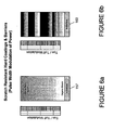
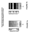
- FIGS 6 and 7 show two examples of multi-layer films that could be produced with two differing forms of modulation, pulse-width and pulse-amplitude modulation. Both of these figures illustrate the film layers deposited on the substrate and the corresponding modulated power signal that is used to generate the plasma. Notice that the power signal is modulated during the deposition process, which differs from establishing and leaving initial set points that are static during the deposition process.
- FIG. 6a it illustrates a variable film 157 produced by pulse-width modulation.
- the cycle between short pulse widths and long pulse widths is relatively long.
- This long cycle produces a variable-gradient coating on the substrate that varies through its thickness from a flexible, organo-silicon film located next to the substrate to a rigid, dense SiO2 or SiOxNy film.
- the film produced by this process becomes harder and more rigid as it extends out from the substrate.
- the pulse width modulation allows a film to be created that bonds well with the substrate but also has a hardened outer portion that resists scratches and that has good barrier properties. This type of film could not be efficiently created without a modulated power signal.
- FIG. 6b illustrates this type of substrate and film 160.
- the cycle between short pulse widths and long pulse widths is relatively short, thereby creating multiple layers. These individual layers can also vary from less dense to more dense within a single layer - much as the single gradient layer in Figure 6a does.
- a less-dense, organo-silicon layer is initially deposited on the substrate. This type of layer bonds best with the substrate.
- the next layer is slightly more dense, and the third layer is an almost pure SiO2 or SiOxNy layer, which is extremely dense and hard.
- the pulse width modulates to shorter pulse widths, the next layer is again a less-dense, organo-silicon layer that bonds easily to the dense layer just below.
- This cycle can repeat hundreds or even thousands of times to create a multilayer, gradient film that is extremely hard, resilient, and with good barrier properties. Further, this film can be produced with a minimal amount of heat and damage to the substrate.
- Figures 7a and 7b illustrate another series of films similar to those shown in Figure 6a and 6b. These films, however, are created using pulse-amplitude modulation. Again, both a single gradient film 165 or a multilayer gradient film 170 can be created using modulation techniques. Note that this process works for almost any precursor and is not limited to silicon-based compounds.
- Variable films can be created with other modulation techniques.
- modulation technologies that could be implemented to effectively control the radical species density and electromagnetic radiation in relation to time, including, PWM - Pulse Width Modulation, PAM - Pulse Amplitude Modulation, PPM - Pulse Position Modulation, AM - Amplitude modulation, FM - Frequency Modulation, etc.
- these techniques involve modulating a power signal during film deposition rather than setting an initial power point or duty cycle.
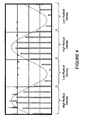
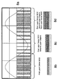
- FIGS 8a through 8d show an example of pulse-width modulation and its possible affects on the films properties for Si02 and or SiOxNy.
- a sign wave signal is used to drive the pulsing frequency at a fixed peak power level to increase or decrease the short term average power into the plasma.
- the sign wave shown is the drive signal, and it also indicates power.
- the modulation increases the power level per given time interval by increasing the on-time and decreasing the off-time of the plasma, thus increasing the instantaneous radical density and electromagnetic components of the plasma.
- This process increases the radical density to the point at which all material was converted and deposited and a new material is the dominate contributor to the growing film stack, SiO2 or SiOxNy.
- Figure 8b shows the dense layer formed next to the substrate during this phase.
- Figure 8c shows the less-dense, more-organic layer formed during the second phase. This layer is deposited on the first layer.
- modulation techniques can be used during inline or dynamic deposition processes. By utilizing these modulation techniques with the dynamic deposition process, it is possible to produce alignment layers for applications such as LCD displays, thereby replacing the polymide layers presently being used.
- this discovery allows the user to achieve PECVD films not possible in the past, possibly with extended film properties and qualities not possible to date.
- the higher quality thin films are achieved from the ability to actively control the plasmas radical / electromagnetic radiation densities in continuous way per unit time by contouring the average and or peak power level per time interval.
- the drive waveform can be any waveform or even an arbitrary function. This technique can also be used to control the localized etching rate when the source and system is configured to do so.
- the present invention provides, among other things, a system and method for controlling deposition onto substrates.
- Those skilled in the art can readily recognize that numerous variations and substitutions may be made in the invention, its use and its configuration to achieve substantially the same results as achieved by the embodiments described herein. Accordingly, there is no intention to limit the invention to the disclosed exemplary forms. Many variations, modifications and alternative constructions fall within the scope and spirit of the disclosed invention as expressed in the claims.
Landscapes
- Chemical & Material Sciences (AREA)
- Engineering & Computer Science (AREA)
- Materials Engineering (AREA)
- General Chemical & Material Sciences (AREA)
- Chemical Kinetics & Catalysis (AREA)
- Mechanical Engineering (AREA)
- Metallurgy (AREA)
- Organic Chemistry (AREA)
- Plasma & Fusion (AREA)
- Physics & Mathematics (AREA)
- Inorganic Chemistry (AREA)
- Analytical Chemistry (AREA)
- Chemical Vapour Deposition (AREA)
Abstract
Description
- The present invention relates to power supplies, systems, and methods for chemical vapor deposition.
- Chemical vapor deposition (CVD) is a process whereby a film is deposited on a substrate by reacting chemicals together in the gaseous or vapor phase to form a film. The gases or vapors utilized for CVD are gases or compounds that contain the element to be deposited and that may be induced to react with a substrate or other gas(es) to deposit a film. The CVD reaction may be thermally activated, plasma induced, plasma enhanced or activated by light in photon induced systems.
- CVD is used extensively in the semiconductor industry to build up wafers. CVD can also be used for coating larger substrates such as glass and polycarbonate sheets. Plasma enhanced CVD (PECVD), for example, is one of the more promising technologies for creating large photovoltaic sheets, LCD screens, and polycarbonate windows for automobiles.
- Figure 1 illustrates a cut away of a
typical PECVD system 100 for large-scale deposition processes - currently up to 2.5 meters wide. This system includes avacuum chamber 105 of which only two walls are illustrated. Thevacuum chamber 105 houses alinear discharge tube 110. Thelinear discharge tube 110 is formed of aninner conductor 115 that is configured to carry a microwave signal, or other signals, into thevacuum chamber 105. This microwave power radiates outward from thelinear discharge antenna 115 and ignites the surroundingsupport gas 120 that is introduced through thesupport gas tube 120. This ignited gas is a plasma and is generally adjacent to thelinear discharge tube 110. Radicals generated by the plasma and electromagnetic radiation disassociate the feedstock gas(es) 130 introduced through thefeedstock gas tube 125 thereby breaking up the feedstock gas to form new molecules. Certain molecules formed during the dissociation process are deposited on thesubstrate 135. The other molecules formed by the dissociation process are waste and are removed through an exhaust port (not shown) - although these molecules tend to occasionally deposit themselves on the substrate. This dissociation process is extremely sensitive to the amount of power used to generate the plasma. - To coat large substrate surface areas rapidly, a substrate carrier (not shown) moves the
substrate 135 through thevacuum chamber 105 at a steady rate, although thesubstrate 135 could be statically coated in some embodiments. As thesubstrate 135 moves through thevacuum chamber 105, the dissociation should continue at a steady rate and target molecules from the disassociated feed gas theoretically deposit on the substrate, thereby forming a uniform film on the substrate. But due to a variety of real-world factors, the films formed by this process are not always uniform. - Nonconductive and conductive films deposited utilizing plasma enhanced chemical vapor sources have been achieved with many types of power sources and system configurations. Most of these sources utilize microwaves, radio frequency (RF), high frequency (HF), or very high frequency (VHF) energy to generate the excited plasma species.
- Those of skill in the art know that for a given process condition and system configuration of PECVD, it is the average power introduced into the plasma discharge that is a major contributing factor to the density of radicalized plasma species produced. These radicalized plasma species are responsible for disassociating the feedstock gas. For typical PECVD processes, the necessary density of produced radicalized species from the plasma must be greater than that required to fully convert all organic materials. Factors such as consumption in the film deposition processes, plasma decomposition processes of the precursor materials, recombination losses, and pumping losses should be taken into consideration.
- Depending upon the power type, configuration and materials utilized, the required power level for producing the necessary density of radicalized plasma species can unduly heat the substrate beyond its physical limits, and possibly render the films and substrate unusable. This primarily occurs in polymer material substrates due to the low melting point of the material.
- To reduce the amount of heat loading of the substrate, a method of high power pulsing into the plasma, with off times in between the pulsing, can be used. This method allows the plasma during the short high energy pulses to reach saturation of the radicalized species required for the film deposition process and loss to occur, while reducing the instantaneous and continuous heating of the substrate through the reduction of other forms of electromagnetic radiation.
- Film property requirements are achieved by setting the process conditions for deposition, including the power levels, pulsing frequency and duty cycle of the source. To achieve required film properties the structure and structural content of the deposited film must be controlled. The film properties can be controlled by varying the radical species content, (among other important process parameters), and as stated in the above, the radical density is controlled primarily by the average and peak power levels into the plasma discharge.
- To achieve several important film properties, and promote adhesion to some types of substrates, the films organic content must be finely controlled, or possibly the contents must be in the form of a gradient across the entire film thickness. Current technology, which enables control of only certain process parameters, cannot achieve this fine control. For example, current technology consists of changing the deposition conditions, usually manually or by multiple sources and chambers with differing process conditions, creating steps in the film stack up to achieve a gradient type stack. Primarily the precursor vapor content, system pressure, and or power level at one or more times is used to develop a stack of layers. These methods are crude at best and do not enable fine control. Accordingly, a new system and method are needed to address this and other problems with the existing technology.
- Exemplary embodiments of the present invention that are shown in the drawings are summarized below. These and other embodiments are more fully described in the Detailed Description section. It is to be understood, however, that there is no intention to limit the invention to the forms described in this Summary of the Invention or in the Detailed Description. One skilled in the art can recognize that there are numerous modifications, equivalents and alternative constructions that fall within the spirit and scope of the invention as expressed in the claims.
- One embodiment includes generating a first electrical pulse having a first pulse amplitude; using the first electrical pulse to generate a first density of radicalized species; disassociating a feedstock gas using the radicalized species in the first density of radicalized species, thereby creating a first deposition material; depositing the first deposition material on a substrate; generating a second electrical pulse having a second pulse amplitude, wherein the second pulse amplitude is different from the first pulse width; using the second electrical pulse to generate a second density of radicalized species; disassociating a feedstock gas using the radicalized species in the second density of radicalized species, thereby creating a second deposition material; and depositing the second plurality of deposition materials on the first deposition material.
- Various objects and advantages and a more complete understanding of the present invention are apparent and more readily appreciated by reference to the following Detailed Description and to the appended claims when taken in conjunction with the accompanying Drawing wherein:
- Figure 1 illustrates one type of PECVD system;
- Figure 2a illustrates a power supply for a PECVD system in accordance with one embodiment of the present invention;
- Figure 2b is an alternative depiction of a power supply for a PECVD system in accordance with one embodiment of the present invention;
- Figure 3 illustrates one example of a pulse-width modulated power signal;
- Figure 4 illustrates one example of a pulse-amplitude modulated power signal;
- Figure 5 illustrates one example of a frequency-modulated power signal;
- Figure 6a illustrates one example of a gradient film formed using pulse-width modulation;
- Figure 6b illustrates one example of a multi-layer gradient film formed using pulse-width modulation;
- Figure 7a illustrates one example of a gradient film formed using amplitude-width modulation;
- Figure 7b illustrates one example of a multi-layer gradient film formed using amplitude-width modulation; and
- Figures 8a-8d illustrate the development of a multi-layer gradient film over time using a pulse-width modulated power signal.
- In some PECVD processes the typical radical lifetime (time for the loss of and consumption of the radical species) is long enough so that there can be an off time of the plasma during which the radical density remaining is gradually consumed by the deposition of the film and loss mechanisms. Therefore, by controlling the total radical density during these on and off times of the plasma the chemical makeup of the film can be altered, as well as the over all layer properties of the film.
- By modulating the power level into the plasma, the on time of the plasma and the timing between the power pulses, the user can make films that were not achievable before in PECVD. The layers could be a single gradient layer or a multiple stack of hundreds to thousands of micro layers with varying properties between each layer. Both processes can create a unique film.
- Figure 2a illustrates a system constructed in accordance with one embodiment of the present invention. This system includes a
DC source 140 that is controllable by thepulse control 145. The terms "DC source" and "DC power supply" refer to any type of power supply, including those that use a linear amplifier, a non-linear amplifier, or no amplifier. TheDC source 145 powers themagnetron 150, which generates the microwaves, or other energy waves, that drive the inner conductor within the linear discharge tube (not shown). Thepulse control 145 can contour the shape of the DC pulses and adjust the set points for pulse properties such as duty cycle, frequency, and amplitude. The process of contouring the shape of the DC pulses is described in the commonly owned and assigned attorney docket number APPL-008/00US (corresponding toUS Serial No. 11/264,540 - The
pulse control 145 is also configured to modulate the DC pulses, or other energy signal, driving themagnetron 150 during the operation of the PECVD device. In some embodiments, thepulse control 145 can be configured to only modulate the signal driving themagnetron 150. In either embodiment, however, by modulating the DC pulses, the power level into the plasma can also be modulated, thereby enabling the user to control radical density and make films that were not achievable before in PECVD. This system can be used to form variable, single gradient layers or a multiple stack of hundreds to thousands of micro layers with varying properties between each other. - Figure 2b illustrates an alternate embodiment of a power supply. This embodiment includes an
arbitrary waveform generator 141, anamplifier 142, apulse control 145, amagnetron 150, and aplasma source antenna 152. In operation, thearbitrary waveform generator 141 generates a waveform and corresponding voltage that can be in virtually any form. Next, theamplifier 142 amplifies the voltage from the arbitrary waveform generator to a usable amount. In the case of a microwave generator (e.g., the magnetron 150) the signal could be amplified from +/_ 5VDC to 5,000 VDC. Next, the high voltage signature is applied to themagnetron 150, which is a high frequency generator. Themagnetron 150 generates a power output carrier (at 2.45GHZ in this case) that has its amplitude and or frequency varied based upon the originally generated voltage signature. Finally, the output from the magnetron is applied to thesource 152 to generate a power modulated plasma. - Signal modulation can be applied by the
pulse control 145 to thearbitrary waveform generator 141. Signal modulation is a well-known process in many fields - the most well known being FM (frequency modulated) and AM (amplitude modulated) radio. But modulation has not been used before to control film properties and create layers during PECVD. Many forms of modulation exist that could be applied to a waveform power level, duty cycle or frequency, but only a few are described below. Those of skill in the art will recognize other methods. Note that modulation is different from simply increasing or decreasing the power or duty cycle of a power signal into a source. - Figure 3 illustrates pulse-width modulation, which varies the width of pulse widths over time. With pulse-width modulation, the value of a sample of data is represented by the length of a pulse.
- Figure 4 illustrates pulse-amplitude modulation, which is a form of signal modulation in which the message information is encoded in the amplitude of a series of signal pulses. In the case of plasma sources the voltage, current or power level can be amplitude modulated by whatever percentage desired.
- Figure 5 illustrates frequency modulation (FM), which is the encoding of information in either analog or digital form into a carrier wave by variation of its instantaneous frequency in accordance with an input signal.
- Referring now to Figures 6 and 7, they show two examples of multi-layer films that could be produced with two differing forms of modulation, pulse-width and pulse-amplitude modulation. Both of these figures illustrate the film layers deposited on the substrate and the corresponding modulated power signal that is used to generate the plasma. Notice that the power signal is modulated during the deposition process, which differs from establishing and leaving initial set points that are static during the deposition process.
- Referring first to Figure 6a, it illustrates a
variable film 157 produced by pulse-width modulation. In this embodiment, the cycle between short pulse widths and long pulse widths is relatively long. This long cycle produces a variable-gradient coating on the substrate that varies through its thickness from a flexible, organo-silicon film located next to the substrate to a rigid, dense SiO2 or SiOxNy film. The film produced by this process becomes harder and more rigid as it extends out from the substrate. - A benefit is realized with this single, variable gradient layer because the flexible, softer portion of the film bonds better to the substrate than would the dense, rigid portion. Thus, the pulse width modulation allows a film to be created that bonds well with the substrate but also has a hardened outer portion that resists scratches and that has good barrier properties. This type of film could not be efficiently created without a modulated power signal.
- By changing the modulation of the power signal, a multilayer gradient coating can be deposited on the substrate. Figure 6b illustrates this type of substrate and
film 160. In this embodiment, the cycle between short pulse widths and long pulse widths is relatively short, thereby creating multiple layers. These individual layers can also vary from less dense to more dense within a single layer - much as the single gradient layer in Figure 6a does. - In this embodiment, a less-dense, organo-silicon layer is initially deposited on the substrate. This type of layer bonds best with the substrate. The next layer is slightly more dense, and the third layer is an almost pure SiO2 or SiOxNy layer, which is extremely dense and hard. As the pulse width modulates to shorter pulse widths, the next layer is again a less-dense, organo-silicon layer that bonds easily to the dense layer just below. This cycle can repeat hundreds or even thousands of times to create a multilayer, gradient film that is extremely hard, resilient, and with good barrier properties. Further, this film can be produced with a minimal amount of heat and damage to the substrate.
- Figures 7a and 7b illustrate another series of films similar to those shown in Figure 6a and 6b. These films, however, are created using pulse-amplitude modulation. Again, both a
single gradient film 165 or amultilayer gradient film 170 can be created using modulation techniques. Note that this process works for almost any precursor and is not limited to silicon-based compounds. - Variable films can be created with other modulation techniques. In fact, there are many modulation technologies that could be implemented to effectively control the radical species density and electromagnetic radiation in relation to time, including, PWM - Pulse Width Modulation, PAM - Pulse Amplitude Modulation, PPM - Pulse Position Modulation, AM - Amplitude modulation, FM - Frequency Modulation, etc. Again, these techniques involve modulating a power signal during film deposition rather than setting an initial power point or duty cycle.
- Referring now to Figures 8a through 8d, they show an example of pulse-width modulation and its possible affects on the films properties for Si02 and or SiOxNy. A sign wave signal is used to drive the pulsing frequency at a fixed peak power level to increase or decrease the short term average power into the plasma. The sign wave shown is the drive signal, and it also indicates power.
- At the beginning portion (left side) of the Figure 8a, the modulation increases the power level per given time interval by increasing the on-time and decreasing the off-time of the plasma, thus increasing the instantaneous radical density and electromagnetic components of the plasma. This process increases the radical density to the point at which all material was converted and deposited and a new material is the dominate contributor to the growing film stack, SiO2 or SiOxNy. Figure 8b shows the dense layer formed next to the substrate during this phase.
- In the center of the drive signal, the on-time is at its lowest and off-time at its highest value. This effect decreases the instantaneous radical density to the point at which all material was consumed and the precursor material again becomes the dominate contributor to the growing film stack. Figure 8c shows the less-dense, more-organic layer formed during the second phase. This layer is deposited on the first layer.
- Finally in the last portion of the waveform, the process returns to saturation of the radical density like in the first portion of the waveform. This phase deposits a hardened, dense layer. Figure 8d shows the dense, third layer deposited on the second layer. Accordingly, the three phases together leaving an inter layer of organic material between two hard, dense layers - thereby introducing flexibility into the entire film stack.
- These modulation techniques can be used during inline or dynamic deposition processes. By utilizing these modulation techniques with the dynamic deposition process, it is possible to produce alignment layers for applications such as LCD displays, thereby replacing the polymide layers presently being used.
- In summary, this discovery allows the user to achieve PECVD films not possible in the past, possibly with extended film properties and qualities not possible to date. The higher quality thin films are achieved from the ability to actively control the plasmas radical / electromagnetic radiation densities in continuous way per unit time by contouring the average and or peak power level per time interval. The drive waveform can be any waveform or even an arbitrary function. This technique can also be used to control the localized etching rate when the source and system is configured to do so.
- In conclusion, the present invention provides, among other things, a system and method for controlling deposition onto substrates. Those skilled in the art can readily recognize that numerous variations and substitutions may be made in the invention, its use and its configuration to achieve substantially the same results as achieved by the embodiments described herein. Accordingly, there is no intention to limit the invention to the disclosed exemplary forms. Many variations, modifications and alternative constructions fall within the scope and spirit of the disclosed invention as expressed in the claims.
Claims (33)
- A method of generating a film during a chemical vapor deposition process, the method comprising:generating a first electrical pulse having a first pulse width;using the first electrical pulse, generating a first density of radicalized species;disassociating a first portion of a feedstock gas using the first density of radicalized species, thereby creating deposition materials;depositing the deposition material on a substrate as a first layer;generating a second electrical pulse having a second pulse width, wherein the second pulse width is different from the first pulse width;using the second electrical pulse, generating a second density of radicalized species;disassociating a second portion of a feedstock gas using the radicalized species in the second density of radicalized species, thereby creating a second plurality of deposition materials; anddepositing the deposition material on the first layer.
- A method of controlling a chemical vapor deposition process, the method comprising:generating a plasma having a density of radicalized species, wherein the plasma is generated using a power signal;disassociating a first portion of a feedstock gas using the radicalized species in the first density of radicalized species, thereby creating a first deposition material;depositing the first deposition material on a substrate, thereby forming a first layer;modifying the density of radicalized species by modulating the power signal used to generate the plasma;disassociating a second portion of the feedstock gas using the radicalized species in the modified density of radicalized species, thereby creating a second deposition material anddepositing the second deposition material on the first layer, thereby forming a second layer.
- The method of claim 2, further comprising:modifying the density of radicalized species by modulating the power signal used to generate the plasma, thereby creating a third density of radicalized species;disassociating a third portion of the feedstock gas using the third density of radicalized species, thereby creating a third deposition material; anddepositing the third deposition material on the second layer, thereby forming a third layer.
- The method of claim 2, wherein the first layer and the second layer comprise separate layers of deposition material within a film deposited on the substrate.
- The method of claim 2, wherein the first layer and the formed second layer comprises a single gradient stack deposited on the substrate.
- The method of claim 2, wherein modifying the density of radicalized species by modulating the power signal used to generate the plasma comprises:modulating an amplitude characteristic of the power signal used to generate the plasma.
- The method of claim 2, wherein modifying the density of radicalized species by modulating the power signal used to generate the plasma comprises:modulating a frequency characteristic of the power signal used to generate the plasma.
- The method of claim 2, wherein modifying the density of radicalized species by modulating the power signal used to generate the plasma comprises:modulating a pulse width characteristic of the power signal used to generate the plasma.
- The method of claim 2, wherein modifying the density of radicalized species by modulating the power signal used to generate the plasma comprises:modulating a pulse position characteristic of the power signal used to generate the plasma.
- The method of claim 2, wherein the power signal comprises a high-frequency signal for generating the plasma.
- The method of claim 2, wherein the power signal is usable by a high-frequency generator so that the high-frequency generator can generate a high-frequency signal for generating the plasma.
- The method of claim 11, wherein the high-frequency signal comprises microwaves.
- A method of generating a film during a chemical vapor deposition process, the method comprising:generating a first electrical pulse having a first pulse amplitude;using the first electrical pulse to generate a first density of radicalized species;disassociating a first portion of a feedstock gas using the radicalized species in the first density of radicalized species, thereby creating a first deposition material;depositing the first deposition material on a substrate;generating a second electrical pulse having a second pulse amplitude, wherein the second pulse amplitude is different from the first pulse width;using the second electrical pulse to generate a second density of radicalized species;disassociating a second portion of the feedstock gas using the radicalized species in the second density of radicalized species, thereby creating a second deposition material; anddepositing the second plurality of deposition materials on the first deposition material.
- A method of generating a film during a chemical vapor deposition process, the method comprising:using a first electrical pulse to generate a plasma with a first density of radicalized species;disassociating a first portion of a feedstock gas using the radicalized species in the first density of radicalized species, thereby creating a first deposition material;depositing the first deposition material on a substrate;using a second electrical pulse to create a second density of radicalized species within the plasma, wherein the second density is less than the first density;disassociating a second portion of the feedstock gas using the second density of radicalized species, thereby creating a second deposition material; anddepositing the second deposition materials on the first deposition material.
- The method of claim 14, wherein the first electrical pulse is associated with a first pulse width, the method further comprising:generating a second electrical pulse with a second pulse width, the second pulse width being greater than the first pulse width.
- The method of claim 14, wherein the first electrical pulse is associated with a first pulse width, the method further comprising:generating a second electrical pulse with a second pulse width, the second pulse width being less than the first pulse width.
- The method of claim 14, wherein the first electrical pulse is associated with a first pulse amplitude, the method further comprising:generating a second electrical pulse with a second pulse amplitude, the second pulse amplitude being less than the first pulse amplitude.
- The method of claim 14, wherein the first electrical pulse is associated with a first pulse position, the method further comprising:generating a second electrical pulse with a second pulse position, the second pulse position being less than the first pulse position.
- The method of claim 14, wherein using a first electrical pulse to generate a plasma with a first density of radicalized species comprises:generating a high-frequency signal using the first electrical pulse.
- The method of claim 19, wherein using a first electrical pulse to generate a plasma with a first density of radicalized species comprises:introducing the high-frequency signal into a deposition chamber; andgenerating the plasma within the deposition chamber using the high-frequency signal.
- A substrate coated with a thin film, the substrate formed by:generating a first electrical pulse having a first pulse width;using the first electrical pulse, generating a first density of radicalized species;disassociating a first portion of a feedstock gas using the first density of radicalized species, thereby creating a first plurality of deposition materials;depositing the first plurality of deposition materials on the substrate as a first layer;generating a second electrical pulse having a second pulse width, wherein the second pulse width is different from the first pulse width;using the second electrical pulse, generating a second density of radicalized species;disassociating a second portion of a feedstock gas using the radicalized species in the second density of radicalized species, thereby creating a second plurality of deposition materials; anddepositing the second plurality of deposition materials on the first layer.
- A substrate coated with a thin film, the substrate formed by:generating a plasma having a density of radicalized species, wherein the plasma is generated using a power signal;disassociating a first portion of a feedstock gas using the radicalized species in the first density of radicalized species, thereby creating a first deposition material;depositing the first deposition material on the substrate, thereby forming a first layer;modifying the density of radicalized species by modulating the power signal used to generate the plasma;disassociating a second portion of the feedstock gas using the radicalized species in the modified density of radicalized species, thereby creating a second deposition material; anddepositing the second deposition material on the first layer, thereby forming a second layer.
- The substrate of claim 22, further formed by:modifying the density of radicalized species by modulating the power signal used to generate the plasma, thereby creating a third density of radicalized species;disassociating a third portion of the feedstock gas using the third density of radicalized species, thereby creating a third deposition material; anddepositing the third deposition material on the second layer, thereby forming a third layer.
- The substrate of claim 22, wherein the first layer and the second layer comprise separate layers of deposition material within a film deposited on the substrate.
- The substrate of claim 22, wherein the first layer and the formed second layer comprises a single gradient stack deposited on the substrate.
- The substrate of claim 22, wherein modifying the density of radicalized species by modulating the power signal used to generate the plasma comprises:modulating an amplitude characteristic of the power signal used to generate the plasma.
- The substrate of claim 22, wherein modifying the density of radicalized species by modulating the power signal used to generate the plasma comprises:modulating a frequency characteristic of the power signal used to generate the plasma.
- The substrate of claim 22, wherein modifying the density of radicalized species by modulating the power signal used to generate the plasma comprises:modulating a pulse width characteristic of the power signal used to generate the plasma.
- The substrate of claim 22, wherein modifying the density of radicalized species by modulating the power signal used to generate the plasma comprises:modulating a pulse position characteristic of the power signal used to generate the plasma.
- The substrate of claim 22, wherein the power signal comprises a high-frequency signal for generating the plasma.
- The substrate of claim 22, wherein the power signal is usable by a high-frequency generator so that the high-frequency generator can generate a high-frequency signal for generating the plasma.
- The substrate of claim 31, wherein the high-frequency signal comprises microwaves.
- A substrate coated with a film, the substrate formed by:generating a first electrical pulse having a first pulse amplitude;using the first electrical pulse to generate a first density of radicalized species;disassociating a first portion of a feedstock gas using the radicalized species in the first density of radicalized species, thereby creating a first deposition material;depositing the first deposition material on the substrate;generating a second electrical pulse having a second pulse amplitude, wherein the second pulse amplitude is different from the first pulse amplitude;using the second electrical pulse to generate a second density of radicalized species;disassociating a second portion of the feedstock gas using the radicalized species in the second density of radicalized species, thereby creating a second deposition material; anddepositing the second plurality of deposition materials on the first deposition material.
Applications Claiming Priority (1)
| Application Number | Priority Date | Filing Date | Title |
|---|---|---|---|
| US11/264,596 US7842355B2 (en) | 2005-11-01 | 2005-11-01 | System and method for modulation of power and power related functions of PECVD discharge sources to achieve new film properties |
Publications (2)
| Publication Number | Publication Date |
|---|---|
| EP1780304A2 true EP1780304A2 (en) | 2007-05-02 |
| EP1780304A3 EP1780304A3 (en) | 2009-11-18 |
Family
ID=37685856
Family Applications (1)
| Application Number | Title | Priority Date | Filing Date |
|---|---|---|---|
| EP06022262A Withdrawn EP1780304A3 (en) | 2005-11-01 | 2006-10-25 | PECVD method with modulation of power |
Country Status (4)
| Country | Link |
|---|---|
| US (2) | US7842355B2 (en) |
| EP (1) | EP1780304A3 (en) |
| CN (1) | CN1958840A (en) |
| TW (1) | TWI346147B (en) |
Cited By (1)
| Publication number | Priority date | Publication date | Assignee | Title |
|---|---|---|---|---|
| WO2014170696A1 (en) * | 2013-04-19 | 2014-10-23 | Gencoa Ltd | Pulse control of deposition and surface treatment processes |
Families Citing this family (17)
| Publication number | Priority date | Publication date | Assignee | Title |
|---|---|---|---|---|
| WO2011006109A2 (en) * | 2008-01-30 | 2011-01-13 | Applied Materials, Inc. | High efficiency low energy microwave ion/electron source |
| US7993733B2 (en) | 2008-02-20 | 2011-08-09 | Applied Materials, Inc. | Index modified coating on polymer substrate |
| US20090238998A1 (en) * | 2008-03-18 | 2009-09-24 | Applied Materials, Inc. | Coaxial microwave assisted deposition and etch systems |
| US8349156B2 (en) * | 2008-05-14 | 2013-01-08 | Applied Materials, Inc. | Microwave-assisted rotatable PVD |
| US20100078315A1 (en) * | 2008-09-26 | 2010-04-01 | Applied Materials, Inc. | Microstrip antenna assisted ipvd |
| US20100078320A1 (en) * | 2008-09-26 | 2010-04-01 | Applied Materials, Inc. | Microwave plasma containment shield shaping |
| KR20110079831A (en) * | 2008-10-03 | 2011-07-08 | 비코 프로세스 이큅먼트, 아이엔씨. | Weather epitaxy system |
| US8659335B2 (en) * | 2009-06-25 | 2014-02-25 | Mks Instruments, Inc. | Method and system for controlling radio frequency power |
| TW201129713A (en) * | 2009-07-09 | 2011-09-01 | Applied Materials Inc | Curved microwave plasma line source for coating of three-dimensional substrates |
| US9388490B2 (en) | 2009-10-26 | 2016-07-12 | General Plasma, Inc. | Rotary magnetron magnet bar and apparatus containing the same for high target utilization |
| WO2011137371A2 (en) * | 2010-04-30 | 2011-11-03 | Applied Materials, Inc. | Vertical inline cvd system |
| JP5865806B2 (en) | 2012-09-05 | 2016-02-17 | 株式会社東芝 | Semiconductor device manufacturing method and semiconductor manufacturing apparatus |
| US9018108B2 (en) | 2013-01-25 | 2015-04-28 | Applied Materials, Inc. | Low shrinkage dielectric films |
| JP6491888B2 (en) * | 2015-01-19 | 2019-03-27 | 株式会社日立ハイテクノロジーズ | Plasma processing method and plasma processing apparatus |
| US10371244B2 (en) | 2015-04-09 | 2019-08-06 | United Technologies Corporation | Additive manufactured gear for a geared architecture gas turbine engine |
| US10858727B2 (en) | 2016-08-19 | 2020-12-08 | Applied Materials, Inc. | High density, low stress amorphous carbon film, and process and equipment for its deposition |
| US12322573B2 (en) * | 2021-05-12 | 2025-06-03 | Applied Materials, Inc. | Pulsing plasma treatment for film densification |
Citations (3)
| Publication number | Priority date | Publication date | Assignee | Title |
|---|---|---|---|---|
| US4837185A (en) * | 1988-10-26 | 1989-06-06 | Intel Corporation | Pulsed dual radio frequency CVD process |
| US5643638A (en) * | 1994-12-20 | 1997-07-01 | Schott Glaswerke | Plasma CVD method of producing a gradient layer |
| US20040206730A1 (en) * | 2003-04-16 | 2004-10-21 | Applied Science & Technology | Toroidal low-field reactive gas and plasma source having a dielectric vacuum vessel |
Family Cites Families (111)
| Publication number | Priority date | Publication date | Assignee | Title |
|---|---|---|---|---|
| US521638A (en) * | 1894-06-19 | oleal | ||
| EP0045822B1 (en) * | 1980-08-08 | 1985-05-29 | Battelle Development Corporation | Cylindrical magnetron sputtering cathode |
| US4422916A (en) * | 1981-02-12 | 1983-12-27 | Shatterproof Glass Corporation | Magnetron cathode sputtering apparatus |
| US4356073A (en) * | 1981-02-12 | 1982-10-26 | Shatterproof Glass Corporation | Magnetron cathode sputtering apparatus |
| DD217964A3 (en) | 1981-10-02 | 1985-01-23 | Ardenne Manfred | DEVICE FOR HIGH-RATE SCREENING ACCORDING TO THE PLASMATRON PRINCIPLE |
| US4417968A (en) * | 1983-03-21 | 1983-11-29 | Shatterproof Glass Corporation | Magnetron cathode sputtering apparatus |
| US4443318A (en) * | 1983-08-17 | 1984-04-17 | Shatterproof Glass Corporation | Cathodic sputtering apparatus |
| US4445997A (en) * | 1983-08-17 | 1984-05-01 | Shatterproof Glass Corporation | Rotatable sputtering apparatus |
| US4466877A (en) * | 1983-10-11 | 1984-08-21 | Shatterproof Glass Corporation | Magnetron cathode sputtering apparatus |
| US4519885A (en) * | 1983-12-27 | 1985-05-28 | Shatterproof Glass Corp. | Method and apparatus for changing sputtering targets in a magnetron sputtering system |
| US4904362A (en) * | 1987-07-24 | 1990-02-27 | Miba Gleitlager Aktiengesellschaft | Bar-shaped magnetron or sputter cathode arrangement |
| US5354446A (en) * | 1988-03-03 | 1994-10-11 | Asahi Glass Company Ltd. | Ceramic rotatable magnetron sputtering cathode target and process for its production |
| DE3821207A1 (en) | 1988-06-23 | 1989-12-28 | Leybold Ag | ARRANGEMENT FOR COATING A SUBSTRATE WITH DIELECTRICS |
| US4927515A (en) * | 1989-01-09 | 1990-05-22 | The Board Of Trustees Of The Leland Stanford Junior University | Circular magnetron sputtering device |
| US5115450A (en) * | 1989-07-06 | 1992-05-19 | Advanced Micro Devices, Inc. | High speed digital to analog to digital communication system |
| US5096562A (en) * | 1989-11-08 | 1992-03-17 | The Boc Group, Inc. | Rotating cylindrical magnetron structure for large area coating |
| US5047131A (en) * | 1989-11-08 | 1991-09-10 | The Boc Group, Inc. | Method for coating substrates with silicon based compounds |
| JP2521558B2 (en) * | 1990-05-18 | 1996-08-07 | 信越化学工業株式会社 | Electrorheological fluid composition |
| BE1003701A3 (en) * | 1990-06-08 | 1992-05-26 | Saint Roch Glaceries | Rotary cathode. |
| WO1992002659A1 (en) * | 1990-08-10 | 1992-02-20 | Viratec Thin Films, Inc. | Shielding for arc suppression in rotating magnetron sputtering systems |
| US5200049A (en) * | 1990-08-10 | 1993-04-06 | Viratec Thin Films, Inc. | Cantilever mount for rotating cylindrical magnetrons |
| JP2687966B2 (en) * | 1990-08-20 | 1997-12-08 | 富士通株式会社 | Method for manufacturing semiconductor device |
| US5156727A (en) * | 1990-10-12 | 1992-10-20 | Viratec Thin Films, Inc. | Film thickness uniformity control apparatus for in-line sputtering systems |
| US5100527A (en) * | 1990-10-18 | 1992-03-31 | Viratec Thin Films, Inc. | Rotating magnetron incorporating a removable cathode |
| US5106474A (en) * | 1990-11-21 | 1992-04-21 | Viratec Thin Films, Inc. | Anode structures for magnetron sputtering apparatus |
| US5108574A (en) * | 1991-01-29 | 1992-04-28 | The Boc Group, Inc. | Cylindrical magnetron shield structure |
| DE4106770C2 (en) * | 1991-03-04 | 1996-10-17 | Leybold Ag | Performing reactive coating of a substrate |
| US5171411A (en) * | 1991-05-21 | 1992-12-15 | The Boc Group, Inc. | Rotating cylindrical magnetron structure with self supporting zinc alloy target |
| DE4117368A1 (en) | 1991-05-28 | 1992-12-03 | Leybold Ag | Sputtering device with rotating magnetron cathode target - concentrates cooling medium pref. water onto target surface heated by plasma |
| US5364518A (en) * | 1991-05-28 | 1994-11-15 | Leybold Aktiengesellschaft | Magnetron cathode for a rotating target |
| DE4117367C2 (en) | 1991-05-28 | 1999-11-04 | Leybold Ag | Method for generating a homogeneous removal profile on a rotating target of a sputtering device |
| US5262032A (en) * | 1991-05-28 | 1993-11-16 | Leybold Aktiengesellschaft | Sputtering apparatus with rotating target and target cooling |
| DE4117518C2 (en) * | 1991-05-29 | 2000-06-21 | Leybold Ag | Device for sputtering with a moving, in particular rotating, target |
| DE4126236C2 (en) * | 1991-08-08 | 2000-01-05 | Leybold Ag | Rotating magnetron cathode and use of a rotating magnetron cathode |
| JPH08977B2 (en) | 1991-08-22 | 1996-01-10 | 日新電機株式会社 | Plasma CVD method and apparatus |
| GB9121665D0 (en) * | 1991-10-11 | 1991-11-27 | Boc Group Plc | Sputtering processes and apparatus |
| GB9121699D0 (en) | 1991-10-11 | 1991-11-27 | Hacker Dennis J | Volume manufacture of low weight/cost fire stop(proof)doors & partitions with 1/2-1-1 1/2-2-3-4 hour capacities |
| BE1007067A3 (en) | 1992-07-15 | 1995-03-07 | Emiel Vanderstraeten Besloten | SPUTTER CATHOD AND METHOD FOR MANUFACTURING THIS CATHOD |
| JP3176188B2 (en) | 1992-09-11 | 2001-06-11 | トウシバビデオプロダクツ プライベート リミテッド | Multiplex signal transmission receiver |
| US5338422A (en) * | 1992-09-29 | 1994-08-16 | The Boc Group, Inc. | Device and method for depositing metal oxide films |
| JPH08506855A (en) | 1993-01-15 | 1996-07-23 | ザ ビーオーシー グループ インコーポレイテッド | Cylindrical magnetron shield structure |
| US5385578A (en) * | 1993-02-18 | 1995-01-31 | Ventritex, Inc. | Electrical connection for medical electrical stimulation electrodes |
| US5344792A (en) * | 1993-03-04 | 1994-09-06 | Micron Technology, Inc. | Pulsed plasma enhanced CVD of metal silicide conductive films such as TiSi2 |
| CA2120875C (en) * | 1993-04-28 | 1999-07-06 | The Boc Group, Inc. | Durable low-emissivity solar control thin film coating |
| CA2123479C (en) * | 1993-07-01 | 1999-07-06 | Peter A. Sieck | Anode structure for magnetron sputtering systems |
| US5648293A (en) * | 1993-07-22 | 1997-07-15 | Nec Corporation | Method of growing an amorphous silicon film |
| DE4324683C1 (en) | 1993-07-22 | 1994-11-17 | Fraunhofer Ges Forschung | Procedure for adapting the generator in bipolar low-pressure glow processes |
| US5403458A (en) | 1993-08-05 | 1995-04-04 | Guardian Industries Corp. | Sputter-coating target and method of use |
| DE69408405T2 (en) * | 1993-11-11 | 1998-08-20 | Nissin Electric Co Ltd | Plasma CVD method and device |
| US5405517A (en) | 1993-12-06 | 1995-04-11 | Curtis M. Lampkin | Magnetron sputtering method and apparatus for compound thin films |
| DE4342766A1 (en) | 1993-12-15 | 1995-06-22 | Andre Dipl Ing Linnenbruegger | Magnetron sputtering unit giving improved removal of target material |
| US5620577A (en) * | 1993-12-30 | 1997-04-15 | Viratec Thin Films, Inc. | Spring-loaded mount for a rotatable sputtering cathode |
| US5567289A (en) * | 1993-12-30 | 1996-10-22 | Viratec Thin Films, Inc. | Rotating floating magnetron dark-space shield and cone end |
| US5616225A (en) * | 1994-03-23 | 1997-04-01 | The Boc Group, Inc. | Use of multiple anodes in a magnetron for improving the uniformity of its plasma |
| DE4418906B4 (en) | 1994-05-31 | 2004-03-25 | Unaxis Deutschland Holding Gmbh | Process for coating a substrate and coating system for carrying it out |
| US5571393A (en) * | 1994-08-24 | 1996-11-05 | Viratec Thin Films, Inc. | Magnet housing for a sputtering cathode |
| US5518592A (en) * | 1994-08-25 | 1996-05-21 | The Boc Group, Inc. | Seal cartridge for a rotatable magnetron |
| US5445721A (en) * | 1994-08-25 | 1995-08-29 | The Boc Group, Inc. | Rotatable magnetron including a replacement target structure |
| ZA956811B (en) * | 1994-09-06 | 1996-05-14 | Boc Group Inc | Dual cylindrical target magnetron with multiple anodes |
| FR2725073B1 (en) | 1994-09-22 | 1996-12-20 | Saint Gobain Vitrage | ROTARY MULTI-TARGET CATHODE SPRAYING CATHODE |
| US5527439A (en) * | 1995-01-23 | 1996-06-18 | The Boc Group, Inc. | Cylindrical magnetron shield structure |
| WO1996034124A1 (en) * | 1995-04-25 | 1996-10-31 | The Boc Group, Inc. | Sputtering system using cylindrical rotating magnetron electrically powered using alternating current |
| DE19623359A1 (en) | 1995-08-17 | 1997-02-20 | Leybold Ag | Device for coating a substrate by vaporisation of a rotary tubular target |
| DE69628441T2 (en) * | 1995-10-13 | 2004-04-29 | Dow Global Technologies, Inc., Midland | METHOD FOR PRODUCING COATED PLASTIC SURFACES |
| US5591314A (en) | 1995-10-27 | 1997-01-07 | Morgan; Steven V. | Apparatus for affixing a rotating cylindrical magnetron target to a spindle |
| FR2745010B1 (en) | 1996-02-20 | 1998-06-12 | Serole Michelle Paparone | TUBULAR OR DERIVATIVE CATHODE SPRAYING TARGET MADE OF MULTIPLE LONGITUDINAL PLATES AND METHOD OF MANUFACTURE THEREOF |
| DE19610253C2 (en) | 1996-03-15 | 1999-01-14 | Fraunhofer Ges Forschung | Atomizing device |
| DE19616187B4 (en) | 1996-04-23 | 2004-03-25 | Fraunhofer-Gesellschaft zur Förderung der angewandten Forschung e.V. | Excitation of electrical gas discharges with voltage pulses |
| DE19717127A1 (en) | 1996-04-23 | 1998-10-29 | Fraunhofer Ges Forschung | Excitation of gas discharge with short voltage pulses |
| DE19634795C2 (en) * | 1996-08-29 | 1999-11-04 | Schott Glas | Plasma CVD system with an array of microwave plasma electrodes and plasma CVD processes |
| JPH10104862A (en) | 1996-09-30 | 1998-04-24 | Kyocera Corp | Manufacturing method of electrophotographic photoreceptor |
| DE19651378A1 (en) * | 1996-12-11 | 1998-06-18 | Leybold Systems Gmbh | Insulating thin film sputter deposition apparatus |
| JP4120974B2 (en) * | 1997-06-17 | 2008-07-16 | キヤノンアネルバ株式会社 | Thin film manufacturing method and thin film manufacturing apparatus |
| JP3559429B2 (en) | 1997-07-02 | 2004-09-02 | 松下電器産業株式会社 | Plasma processing method |
| JPH1129863A (en) * | 1997-07-10 | 1999-02-02 | Canon Inc | Deposition film manufacturing method |
| EP0969238A1 (en) | 1998-06-29 | 2000-01-05 | Sinvaco N.V. | Vacuum tight coupling for tube sections |
| US6126778A (en) * | 1998-07-22 | 2000-10-03 | Micron Technology, Inc. | Beat frequency modulation for plasma generation |
| US5985375A (en) * | 1998-09-03 | 1999-11-16 | Micron Technology, Inc. | Method for pulsed-plasma enhanced vapor deposition |
| WO2000028104A1 (en) * | 1998-11-06 | 2000-05-18 | Scivac | Sputtering apparatus and process for high rate coatings |
| EP1147065B1 (en) | 1998-12-21 | 2003-04-09 | Cardinal CG Company | Soil-resistant coating for glass surfaces |
| DE10004787A1 (en) | 1999-09-14 | 2001-03-15 | Ardenne Anlagentech Gmbh | Vacuum deposition apparatus comprises a tubular magnetron and a process chamber having a lid with an open box shape with an upper side and wall sides which extend between the upper side and the upper wall of the process chamber |
| DE19953470A1 (en) * | 1999-11-05 | 2001-05-23 | Heraeus Gmbh W C | Tube target |
| TW507256B (en) * | 2000-03-13 | 2002-10-21 | Mitsubishi Heavy Ind Ltd | Discharge plasma generating method, discharge plasma generating apparatus, semiconductor device fabrication method, and semiconductor device fabrication apparatus |
| US6582572B2 (en) * | 2000-06-01 | 2003-06-24 | Seagate Technology Llc | Target fabrication method for cylindrical cathodes |
| DE10043748B4 (en) | 2000-09-05 | 2004-01-15 | W. C. Heraeus Gmbh & Co. Kg | Cylindrical sputtering target, process for its production and use |
| AU2001284441A1 (en) | 2000-09-08 | 2002-03-22 | Asahi Glass Company, Limited | Cylindrical target and method of manufacturing the cylindrical target |
| JP4516199B2 (en) * | 2000-09-13 | 2010-08-04 | キヤノンアネルバ株式会社 | Sputtering apparatus and electronic device manufacturing method |
| JP4557400B2 (en) * | 2000-09-14 | 2010-10-06 | キヤノン株式会社 | Method for forming deposited film |
| WO2002027057A2 (en) | 2000-09-25 | 2002-04-04 | Cardinal Cg Company | Sputtering target and method of making same |
| US20020189939A1 (en) * | 2001-06-14 | 2002-12-19 | German John R. | Alternating current rotatable sputter cathode |
| US20020073924A1 (en) * | 2000-12-15 | 2002-06-20 | Chiang Tony P. | Gas introduction system for a reactor |
| DE10063383C1 (en) | 2000-12-19 | 2002-03-14 | Heraeus Gmbh W C | Production of a tubular target used for cathode sputtering devices comprises forming an outer tube by casting a molten material in a mold, in which the mold has a heated core rod formed from an inner tube |
| WO2002084702A2 (en) * | 2001-01-16 | 2002-10-24 | Lampkin Curtis M | Sputtering deposition apparatus and method for depositing surface films |
| US6726804B2 (en) * | 2001-01-22 | 2004-04-27 | Liang-Guo Wang | RF power delivery for plasma processing using modulated power signal |
| US6375815B1 (en) * | 2001-02-17 | 2002-04-23 | David Mark Lynn | Cylindrical magnetron target and apparatus for affixing the target to a rotatable spindle assembly |
| SE521095C2 (en) | 2001-06-08 | 2003-09-30 | Cardinal Cg Co | Reactive sputtering process |
| JP4035298B2 (en) * | 2001-07-18 | 2008-01-16 | キヤノン株式会社 | Plasma processing method, semiconductor device manufacturing method, and semiconductor device |
| JP2003166047A (en) * | 2001-09-20 | 2003-06-13 | Shin Meiwa Ind Co Ltd | Halogen compound film forming method and film forming apparatus, and magnesium fluoride film |
| US6635154B2 (en) * | 2001-11-03 | 2003-10-21 | Intevac, Inc. | Method and apparatus for multi-target sputtering |
| DE10154229B4 (en) * | 2001-11-07 | 2004-08-05 | Applied Films Gmbh & Co. Kg | Device for the regulation of a plasma impedance |
| US6736948B2 (en) | 2002-01-18 | 2004-05-18 | Von Ardenne Anlagentechnik Gmbh | Cylindrical AC/DC magnetron with compliant drive system and improved electrical and thermal isolation |
| DE10213049A1 (en) | 2002-03-22 | 2003-10-02 | Dieter Wurczinger | Rotatable tubular cathode |
| DE10213043B4 (en) | 2002-03-22 | 2008-10-30 | Von Ardenne Anlagentechnik Gmbh | Tubular magnetron and its use |
| US7384471B2 (en) * | 2002-04-17 | 2008-06-10 | Air Products And Chemicals, Inc. | Porogens, porogenated precursors and methods for using the same to provide porous organosilica glass films with low dielectric constants |
| US7247221B2 (en) * | 2002-05-17 | 2007-07-24 | Applied Films Corporation | System and apparatus for control of sputter deposition process |
| ES2252600T3 (en) * | 2002-09-25 | 2006-05-16 | Degussa Ag | METHOD FOR PRODUCING ACID 5-FORMIL-2-FURILBORONIC. |
| KR20050084844A (en) | 2002-10-09 | 2005-08-29 | 도요 세이칸 가부시키가이샤 | Method of forming metal oxide film and microwave power source unit for use in the method |
| US20040112735A1 (en) * | 2002-12-17 | 2004-06-17 | Applied Materials, Inc. | Pulsed magnetron for sputter deposition |
| US6923891B2 (en) * | 2003-01-10 | 2005-08-02 | Nanofilm Technologies International Pte Ltd. | Copper interconnects |
| DE10317208A1 (en) | 2003-04-15 | 2004-11-04 | Robert Bosch Gmbh | Plasma deposition process |
| DE102004014323B4 (en) | 2004-03-22 | 2009-04-02 | Von Ardenne Anlagentechnik Gmbh | Method and device for producing gradient layers or layer sequences by physical sputtering |
-
2005
- 2005-11-01 US US11/264,596 patent/US7842355B2/en not_active Expired - Fee Related
-
2006
- 2006-07-25 US US11/492,628 patent/US20070098893A1/en not_active Abandoned
- 2006-10-17 TW TW095138238A patent/TWI346147B/en not_active IP Right Cessation
- 2006-10-25 EP EP06022262A patent/EP1780304A3/en not_active Withdrawn
- 2006-11-01 CN CNA2006101432493A patent/CN1958840A/en active Pending
Patent Citations (3)
| Publication number | Priority date | Publication date | Assignee | Title |
|---|---|---|---|---|
| US4837185A (en) * | 1988-10-26 | 1989-06-06 | Intel Corporation | Pulsed dual radio frequency CVD process |
| US5643638A (en) * | 1994-12-20 | 1997-07-01 | Schott Glaswerke | Plasma CVD method of producing a gradient layer |
| US20040206730A1 (en) * | 2003-04-16 | 2004-10-21 | Applied Science & Technology | Toroidal low-field reactive gas and plasma source having a dielectric vacuum vessel |
Non-Patent Citations (1)
| Title |
|---|
| TAKEYA M ET AL: "Plasma conditions for as-grown low temperature poly-Si formation on SiO2 substrate by sputtering and plasma enhanced chemical vapor deposition processes", JOURNAL OF VACUUM SCIENCE AND TECHNOLOGY: PART A, AVS /AIP, MELVILLE, NY., US, vol. 16, no. 3, 1 May 1998 (1998-05-01), pages 1917 - 1920, XP012004054, ISSN: 0734-2101, DOI: 10.1116/1.581196 * |
Cited By (1)
| Publication number | Priority date | Publication date | Assignee | Title |
|---|---|---|---|---|
| WO2014170696A1 (en) * | 2013-04-19 | 2014-10-23 | Gencoa Ltd | Pulse control of deposition and surface treatment processes |
Also Published As
| Publication number | Publication date |
|---|---|
| US7842355B2 (en) | 2010-11-30 |
| EP1780304A3 (en) | 2009-11-18 |
| US20070098916A1 (en) | 2007-05-03 |
| TWI346147B (en) | 2011-08-01 |
| US20070098893A1 (en) | 2007-05-03 |
| CN1958840A (en) | 2007-05-09 |
| TW200730662A (en) | 2007-08-16 |
Similar Documents
| Publication | Publication Date | Title |
|---|---|---|
| US7842355B2 (en) | System and method for modulation of power and power related functions of PECVD discharge sources to achieve new film properties | |
| US20080286495A1 (en) | System and method for power function ramping of split antenna pecvd discharge sources | |
| EP3155631B1 (en) | A microwave plasma reactor and method for manufacturing synthetic diamond material | |
| WO2010036489A2 (en) | Microwave plasma containment shield shaping | |
| WO2008052706A1 (en) | Method of forming a film by deposition from a plasma | |
| US7342361B2 (en) | Plasma source | |
| US20110045205A1 (en) | Device and Process for Very High-Frequency Plasma-Assisted CVD under Atmospheric Pressure, and Applications Thereof | |
| TWI912242B (en) | Deposition tool capable of modulating one or more plasma temporally and/or spatially | |
| KR100824171B1 (en) | Method and system for modulation of power and power related functions of a PCCD discharge source to obtain new thin film properties | |
| Liehr et al. | Large area microwave coating technology | |
| US6969953B2 (en) | System and method for inductive coupling of an expanding thermal plasma | |
| JP5120924B2 (en) | Method for producing amorphous carbon film | |
| KR100961361B1 (en) | System and method for controlling electromagnetic radiation in a PCD discharge process | |
| US20120018096A1 (en) | Process chamber having modulated plasma supply | |
| KR100481685B1 (en) | Chemical vapor deposition system at room temperature by electron cyclotron resonance plasma and pulsed dc bias combined system and the preparation method for metal composite film using the same | |
| JP2009280875A (en) | Film deposition system | |
| EP1921658A2 (en) | System and method for shielding during PECVD deposition processes | |
| Engemann | Impact of wide dynamic range plasma sources for advanced plasma processing |
Legal Events
| Date | Code | Title | Description |
|---|---|---|---|
| PUAI | Public reference made under article 153(3) epc to a published international application that has entered the european phase |
Free format text: ORIGINAL CODE: 0009012 |
|
| AK | Designated contracting states |
Kind code of ref document: A2 Designated state(s): AT BE BG CH CY CZ DE DK EE ES FI FR GB GR HU IE IS IT LI LT LU LV MC NL PL PT RO SE SI SK TR |
|
| AX | Request for extension of the european patent |
Extension state: AL BA HR MK YU |
|
| RAP1 | Party data changed (applicant data changed or rights of an application transferred) |
Owner name: APPLIED MATERIALS, INC. |
|
| PUAL | Search report despatched |
Free format text: ORIGINAL CODE: 0009013 |
|
| AK | Designated contracting states |
Kind code of ref document: A3 Designated state(s): AT BE BG CH CY CZ DE DK EE ES FI FR GB GR HU IE IS IT LI LT LU LV MC NL PL PT RO SE SI SK TR |
|
| AX | Request for extension of the european patent |
Extension state: AL BA HR MK RS |
|
| 17P | Request for examination filed |
Effective date: 20100325 |
|
| AKX | Designation fees paid |
Designated state(s): AT BE BG CH CY CZ DE DK EE ES FI FR GB GR HU IE IS IT LI LT LU LV MC NL PL PT RO SE SI SK TR |
|
| 17Q | First examination report despatched |
Effective date: 20110518 |
|
| STAA | Information on the status of an ep patent application or granted ep patent |
Free format text: STATUS: THE APPLICATION IS DEEMED TO BE WITHDRAWN |
|
| 18D | Application deemed to be withdrawn |
Effective date: 20150328 |