EP1778001A2 - Method for applying coating agent and electronic control unit - Google Patents
Method for applying coating agent and electronic control unit Download PDFInfo
- Publication number
- EP1778001A2 EP1778001A2 EP06122536A EP06122536A EP1778001A2 EP 1778001 A2 EP1778001 A2 EP 1778001A2 EP 06122536 A EP06122536 A EP 06122536A EP 06122536 A EP06122536 A EP 06122536A EP 1778001 A2 EP1778001 A2 EP 1778001A2
- Authority
- EP
- European Patent Office
- Prior art keywords
- housing
- circuit board
- electronic circuit
- coating agent
- control unit
- Prior art date
- Legal status (The legal status is an assumption and is not a legal conclusion. Google has not performed a legal analysis and makes no representation as to the accuracy of the status listed.)
- Granted
Links
Images


Classifications
-
- H—ELECTRICITY
- H05—ELECTRIC TECHNIQUES NOT OTHERWISE PROVIDED FOR
- H05K—PRINTED CIRCUITS; CASINGS OR CONSTRUCTIONAL DETAILS OF ELECTRIC APPARATUS; MANUFACTURE OF ASSEMBLAGES OF ELECTRICAL COMPONENTS
- H05K3/00—Apparatus or processes for manufacturing printed circuits
- H05K3/22—Secondary treatment of printed circuits
- H05K3/28—Applying non-metallic protective coatings
- H05K3/284—Applying non-metallic protective coatings for encapsulating mounted components
-
- H—ELECTRICITY
- H05—ELECTRIC TECHNIQUES NOT OTHERWISE PROVIDED FOR
- H05K—PRINTED CIRCUITS; CASINGS OR CONSTRUCTIONAL DETAILS OF ELECTRIC APPARATUS; MANUFACTURE OF ASSEMBLAGES OF ELECTRICAL COMPONENTS
- H05K5/00—Casings, cabinets or drawers for electric apparatus
- H05K5/0026—Casings, cabinets or drawers for electric apparatus provided with connectors and printed circuit boards [PCB], e.g. automotive electronic control units
- H05K5/0043—Casings, cabinets or drawers for electric apparatus provided with connectors and printed circuit boards [PCB], e.g. automotive electronic control units comprising a frame housing mating with two lids wherein the PCB is flat mounted on the frame housing
-
- H—ELECTRICITY
- H05—ELECTRIC TECHNIQUES NOT OTHERWISE PROVIDED FOR
- H05K—PRINTED CIRCUITS; CASINGS OR CONSTRUCTIONAL DETAILS OF ELECTRIC APPARATUS; MANUFACTURE OF ASSEMBLAGES OF ELECTRICAL COMPONENTS
- H05K5/00—Casings, cabinets or drawers for electric apparatus
- H05K5/06—Hermetically-sealed casings
- H05K5/061—Hermetically-sealed casings sealed by a gasket held between a removable cover and a body, e.g. O-ring, packing
-
- H—ELECTRICITY
- H05—ELECTRIC TECHNIQUES NOT OTHERWISE PROVIDED FOR
- H05K—PRINTED CIRCUITS; CASINGS OR CONSTRUCTIONAL DETAILS OF ELECTRIC APPARATUS; MANUFACTURE OF ASSEMBLAGES OF ELECTRICAL COMPONENTS
- H05K5/00—Casings, cabinets or drawers for electric apparatus
- H05K5/06—Hermetically-sealed casings
- H05K5/064—Hermetically-sealed casings sealed by potting, e.g. waterproof resin poured in a rigid casing
-
- H—ELECTRICITY
- H05—ELECTRIC TECHNIQUES NOT OTHERWISE PROVIDED FOR
- H05K—PRINTED CIRCUITS; CASINGS OR CONSTRUCTIONAL DETAILS OF ELECTRIC APPARATUS; MANUFACTURE OF ASSEMBLAGES OF ELECTRICAL COMPONENTS
- H05K1/00—Printed circuits
- H05K1/02—Details
- H05K1/14—Structural association of two or more printed circuits
- H05K1/144—Stacked arrangements of planar printed circuit boards
-
- H—ELECTRICITY
- H05—ELECTRIC TECHNIQUES NOT OTHERWISE PROVIDED FOR
- H05K—PRINTED CIRCUITS; CASINGS OR CONSTRUCTIONAL DETAILS OF ELECTRIC APPARATUS; MANUFACTURE OF ASSEMBLAGES OF ELECTRICAL COMPONENTS
- H05K2201/00—Indexing scheme relating to printed circuits covered by H05K1/00
- H05K2201/10—Details of components or other objects attached to or integrated in a printed circuit board
- H05K2201/10227—Other objects, e.g. metallic pieces
- H05K2201/10295—Metallic connector elements partly mounted in a hole of the PCB
- H05K2201/10303—Pin-in-hole mounted pins
-
- H—ELECTRICITY
- H05—ELECTRIC TECHNIQUES NOT OTHERWISE PROVIDED FOR
- H05K—PRINTED CIRCUITS; CASINGS OR CONSTRUCTIONAL DETAILS OF ELECTRIC APPARATUS; MANUFACTURE OF ASSEMBLAGES OF ELECTRICAL COMPONENTS
- H05K3/00—Apparatus or processes for manufacturing printed circuits
- H05K3/30—Assembling printed circuits with electric components, e.g. with resistors
- H05K3/32—Assembling printed circuits with electric components, e.g. with resistors electrically connecting electric components or wires to printed circuits
- H05K3/34—Assembling printed circuits with electric components, e.g. with resistors electrically connecting electric components or wires to printed circuits by soldering
- H05K3/3447—Lead-in-hole components
-
- Y—GENERAL TAGGING OF NEW TECHNOLOGICAL DEVELOPMENTS; GENERAL TAGGING OF CROSS-SECTIONAL TECHNOLOGIES SPANNING OVER SEVERAL SECTIONS OF THE IPC; TECHNICAL SUBJECTS COVERED BY FORMER USPC CROSS-REFERENCE ART COLLECTIONS [XRACs] AND DIGESTS
- Y10—TECHNICAL SUBJECTS COVERED BY FORMER USPC
- Y10T—TECHNICAL SUBJECTS COVERED BY FORMER US CLASSIFICATION
- Y10T29/00—Metal working
- Y10T29/49—Method of mechanical manufacture
- Y10T29/49002—Electrical device making
- Y10T29/49117—Conductor or circuit manufacturing
- Y10T29/49174—Assembling terminal to elongated conductor
- Y10T29/49181—Assembling terminal to elongated conductor by deforming
- Y10T29/49185—Assembling terminal to elongated conductor by deforming of terminal
- Y10T29/49192—Assembling terminal to elongated conductor by deforming of terminal with insulation removal
Definitions
- the present invention relates to a method for applying a coating agent and to an electronic control unit.
- An electronic control unit includes an electronic circuit board accommodated in a housing.
- various measures are taken to make the housing waterproof.
- Japanese Laid-Open Patent Publication No. 2005-150633 describes an electronic control unit having a waterproof structure.
- space is limited. It is thus important that space be effectively used. Therefore, to increase the mounting freedom of an electronic control unit in a vehicle, the electronic control unit must have higher water resistance. Accordingly, in an electronic control unit having a waterproof structure, it is desirable that the electronic circuit board be coated with an anti-moisture agent.
- the anti-moisture agent may hinder soldering.
- the soldered locations are masked before immersing the electronic circuit board in a coating agent (anti-moisture agent).
- the anti-moisture agent is coated on the electronic circuit board with a brush.
- such masking or coating is troublesome.
- some portions of the electronic circuit board may be left uncoated by the anti-moisture agent. Accordingly, improvements must be made to the application of a coating agent.
- the present invention provides a coating agent application method and an electronic control unit enabling simple application of a coating agent to an electronic circuit board accommodated in a housing without leaving uncoated portions.
- One embodiment of the present invention is a method for applying a coating agent to an electronic circuit board.
- the method includes accommodating the electronic circuit board in a housing, performing an electrical connection process on the electronic circuit board accommodated in the housing, and filling the coating agent into the housing and immersing the electronic circuit board in the coating agent.
- Another embodiment of the present invention is an electronic control unit including a housing capable of containing a coating agent and including a bottom for holding the coating agent.
- An electronic circuit board is accommodated in the housing.
- the housing includes an opening enabling insertion of a nozzle for drawing the coating agent into and out of the housing.
- the electronic circuit board includes an insertion portion for guiding the nozzle to the bottom of the housing.
- a further embodiment of the present invention is an electronic control unit including a housing capable of containing a coating agent.
- An electronic circuit board accommodated in the housing includes an electrical bonding portion.
- the housing has an inner bottom surface for supporting the electronic circuit board.
- the inner bottom surface includes a recess for accommodating the electrical bonding portion to immerse the electrical bonding portion in the coating agent.
- Fig. 1 is a perspective view showing the electronic control unit 1
- Fig. 2 is a cross-sectional view taken along line II-II in Fig. 1
- Fig. 3 is an exploded perspective view showing the electronic control unit 1 of Fig. 1.
- a housing 2 includes a hollow housing body 3, a plate-shaped cover 4, and a base 5.
- the cover 4 and base 5 respectively close openings 3a and 3b of the housing body 3.
- a seal 6 is arranged between the cover 4 and the opening 3a of the housing body 3 and between the base 5 and opening 3b of the housing body 3.
- seal grooves 7 extend about the opening 3a on one end of the housing body 3 and on the base 5. Each seal groove 7 receives the corresponding seal 6.
- the housing body 3 has side walls 8 from which a plurality of flanges 9 extend.
- the cover 4 and the base 5 are fastened to the flanges 9 to close the openings 3a and 3b of the housing body 3.
- the seals 6 hermetically seal the gaps between the housing body 3 and the cover 4 and base 5.
- an electronic circuit board 10 has a double-board structure including two boards 10a and 10b.
- the boards 10a and 10b are electrically connected to each other by a plurality of connection terminals 11 and are arranged generally parallel to the cover 4 and the base 5.
- the housing body 3 has an inner wall surface 3c from which a plate-shaped support 12 extends.
- the board 10a is fastened to the support 12 and mounted on the housing body 3.
- the boards 10a and 10b respectively have connection holes 13a and 13b.
- Each of the connection terminals 11 has one end inserted in a connection hole 13a of the board 10a and another end inserted in a connection hole 13b of the board 10b. The two ends of each connection terminal 11 are soldered and electrically connected to the boards 10a and 10b.
- hollow connectors 14 for connection of wire harnesses are formed on the side wall 8 of the housing body 3.
- the connector 14 includes a plurality of connector terminals 15, which extend into the housing 2 through the side wall 8.
- the end of each connector terminal 15 extended into the housing 2 is electrically connected to the electronic circuit board 10 accommodated in the housing 2. More specifically, each connector terminal 15 has a portion bent to be L-shaped and extended toward the board 10a. The L-shaped portion has an end inserted into a connection hole 13c of the board 10a. This end is soldered to the board 10a so that the connector terminal 15 is connected to the board 10a.
- external wires (not shown) in a wire harness connected to the connector 14 are connected to the electronic circuit board 10.
- the base 5 is made of a metal having a high heat dissipation property.
- the base 5 has an inner bottom surface 17 including a recess 19 formed in correspondence with portions of the connection terminals 11 that are soldered. Such soldered portions define electrical bonding portions 18.
- the electrical bonding portions 18, which extend from the board 10b toward the base 5, are arranged in the recess 19. This keeps the surface of the board 10b in close contact with the inner bottom surface 17 of the base 5 and enables effective heat dissipation.
- the electronic circuit board 10 is mounted on the housing 2.
- An electrical connection process (soldering) is performed to connect the boards 10a and 10b to each other.
- a coating agent (anti-moisture agent) is filled into the housing 2.
- the electronic circuit board 10 is immersed in the coating agent inside the housing 2. This coats the electronic circuit board 10.
- the electronic circuit boards 10 (boards 10a and 10b) are mounted on the housing body 3 and undergo electrical connection.
- the base 5 is coupled to the housing body 3. This hermetically seals the opening 3b of the housing body 3.
- the coating agent is filled into the housing 2 from the opening 3a.
- the base 5 functions to hold the coating agent against the direction of gravitational force.
- the coating agent uses a polyolefin resin as a main component and methylcyclohexane as a solvent.
- the coating agent is injected into the housing 2 through a nozzle 20, which is inserted into the housing 2 from the opening 3a.
- the boards 10a and 10b respectively have cutout portions 21a and 21b functioning as nozzle insertion portions enabling insertion of the nozzle 20 toward the vicinity of the base 5.
- An insertion hole 12a is formed in the support 12 at a position corresponding to the cutout portions 21a and 21b of the boards 10a and 10b.
- the recess 19 formed in the inner bottom surface 17 of the base 5 extend to positions corresponding to the cutout portions 21a and 21b.
- the coating agent is injected into the housing 2 in a state in which an outlet 20a of the nozzle 20 is arranged in the recess 19. After the electronic circuit board 10 is immersed in the coating agent inside the housing 2, the coating agent is discharged from the housing 2 through the nozzle 20. This completes the coating process.
- the electronic control unit 1 of the preferred embodiment has the advantages described below.
- a housing is not limited to the housing 2, which includes the housing body 3, the cover 4, and the base 5. Any housing may be used as long as it can contain a coating agent.
- the base 5 does not have to be the bottom of a housing.
- the bottom refers to any portion of a housing that holds a coating agent against the direction of gravitational force when the coating agent is injected into the housing.
- the coating agent may be drawn into and out of the housing 2 through an opening formed in any part of the housing 2.
- a nozzle does not have to be used and the coating agent may be discharged from the housing 2 by inclining the housing 2.
- the nozzle insertions portions do not have to be formed by the cutout portions 21a and 21b and may be holes formed in the boards 10a and 10b.
- a method for easily applying a coating agent to an electronic circuit board accommodated in a housing without leaving uncoated portions includes mounting the electronic circuit board (10) to the housing (2), performing an electrical connection process in the electronic circuit board (10), and filling the housing (2) with the coating agent (anti-moisture agent) to immerse the electronic circuit board (10) in the coating agent.
Landscapes
- Engineering & Computer Science (AREA)
- Microelectronics & Electronic Packaging (AREA)
- Manufacturing & Machinery (AREA)
- Non-Metallic Protective Coatings For Printed Circuits (AREA)
- Casings For Electric Apparatus (AREA)
- Structure Of Printed Boards (AREA)
Abstract
Description
- The present invention relates to a method for applying a coating agent and to an electronic control unit.
- An electronic control unit includes an electronic circuit board accommodated in a housing. In the prior art, various measures are taken to make the housing waterproof. For example,
Japanese Laid-Open Patent Publication No. 2005-150633 - However, in cases in which there are locations that must undergo soldering after the electronic circuit board is mounted on the housing, the anti-moisture agent may hinder soldering. Thus, in the prior art, the soldered locations are masked before immersing the electronic circuit board in a coating agent (anti-moisture agent). Alternatively, after mounting the electronic circuit boards to the housing, the anti-moisture agent is coated on the electronic circuit board with a brush. However, such masking or coating is troublesome. Further, depending on how the electronic circuit board is accommodated in the housing, some portions of the electronic circuit board may be left uncoated by the anti-moisture agent. Accordingly, improvements must be made to the application of a coating agent.
- The present invention provides a coating agent application method and an electronic control unit enabling simple application of a coating agent to an electronic circuit board accommodated in a housing without leaving uncoated portions.
- One embodiment of the present invention is a method for applying a coating agent to an electronic circuit board. The method includes accommodating the electronic circuit board in a housing, performing an electrical connection process on the electronic circuit board accommodated in the housing, and filling the coating agent into the housing and immersing the electronic circuit board in the coating agent.
- Another embodiment of the present invention is an electronic control unit including a housing capable of containing a coating agent and including a bottom for holding the coating agent. An electronic circuit board is accommodated in the housing. The housing includes an opening enabling insertion of a nozzle for drawing the coating agent into and out of the housing. The electronic circuit board includes an insertion portion for guiding the nozzle to the bottom of the housing.
- A further embodiment of the present invention is an electronic control unit including a housing capable of containing a coating agent. An electronic circuit board accommodated in the housing includes an electrical bonding portion. The housing has an inner bottom surface for supporting the electronic circuit board. The inner bottom surface includes a recess for accommodating the electrical bonding portion to immerse the electrical bonding portion in the coating agent.
- Other embodiments and advantages of the present invention will become apparent from the following description, taken in conjunction with the accompanying drawings, illustrating by way of example the principles of the invention.
- The invention, together with objects and advantages thereof, may best be understood by reference to the following description of the presently preferred embodiments together with the accompanying drawings in which:
- Fig. 1 is a perspective view showing an electronic control unit according to a preferred embodiment of the present invention;
- Fig. 2 is a cross-sectional view taken along line II-II in Fig. 1;
- Fig. 3 is an exploded perspective view showing the electronic control unit of Fig. 1;
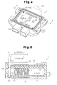
- Fig. 4 is a perspective view showing the procedures for applying a coating agent in the preferred embodiment; and
- Fig. 5 is a cross-sectional view taken along line V-V in Fig. 4.
- In the drawings, like numerals are used for like elements throughout.
- An
electronic control unit 1 and a method for applying a coating agent according to a preferred embodiment of the present invention will now be described with reference to the drawings. - Fig. 1 is a perspective view showing the
electronic control unit 1, Fig. 2 is a cross-sectional view taken along line II-II in Fig. 1, and Fig. 3 is an exploded perspective view showing theelectronic control unit 1 of Fig. 1. As shown in Figs. 1 to 3, ahousing 2 includes ahollow housing body 3, a plate-shaped cover 4, and a base 5. Thecover 4 and base 5 respectively closeopenings 3a and 3b of thehousing body 3. Aseal 6 is arranged between thecover 4 and the opening 3a of thehousing body 3 and between the base 5 and opening 3b of thehousing body 3. In the preferred embodiment,seal grooves 7 extend about the opening 3a on one end of thehousing body 3 and on the base 5. Eachseal groove 7 receives thecorresponding seal 6. Thehousing body 3 hasside walls 8 from which a plurality offlanges 9 extend. Thecover 4 and the base 5 are fastened to theflanges 9 to close theopenings 3a and 3b of thehousing body 3. Theseals 6 hermetically seal the gaps between thehousing body 3 and thecover 4 and base 5. - Referring to Fig. 3, in the preferred embodiment, an
electronic circuit board 10 has a double-board structure including twoboards boards connection terminals 11 and are arranged generally parallel to thecover 4 and the base 5. In the preferred embodiment, thehousing body 3 has aninner wall surface 3c from which a plate-shaped support 12 extends. Theboard 10a is fastened to thesupport 12 and mounted on thehousing body 3. Further, theboards connection holes connection terminals 11 has one end inserted in aconnection hole 13a of theboard 10a and another end inserted in aconnection hole 13b of theboard 10b. The two ends of eachconnection terminal 11 are soldered and electrically connected to theboards - In the preferred embodiment,
hollow connectors 14 for connection of wire harnesses (not shown) are formed on theside wall 8 of thehousing body 3. Theconnector 14 includes a plurality ofconnector terminals 15, which extend into thehousing 2 through theside wall 8. The end of eachconnector terminal 15 extended into thehousing 2 is electrically connected to theelectronic circuit board 10 accommodated in thehousing 2. More specifically, eachconnector terminal 15 has a portion bent to be L-shaped and extended toward theboard 10a. The L-shaped portion has an end inserted into aconnection hole 13c of theboard 10a. This end is soldered to theboard 10a so that theconnector terminal 15 is connected to theboard 10a. As a result, external wires (not shown) in a wire harness connected to theconnector 14 are connected to theelectronic circuit board 10. - In the preferred embodiment, the base 5 is made of a metal having a high heat dissipation property. The base 5, which is in contact with the
board 10b, functions as a heat sink that dissipates heat generated byelectronic components 16 on theboard 10b out of thehousing 2. More specifically, in the preferred embodiment, the base 5 has aninner bottom surface 17 including arecess 19 formed in correspondence with portions of theconnection terminals 11 that are soldered. Such soldered portions defineelectrical bonding portions 18. Theelectrical bonding portions 18, which extend from theboard 10b toward the base 5, are arranged in therecess 19. This keeps the surface of theboard 10b in close contact with theinner bottom surface 17 of the base 5 and enables effective heat dissipation. - A method for applying a coating agent to the
electronic circuit board 10 will now be described with reference to Figs. 4 and 5. - Referring to Figs. 4 and 5, in the preferred embodiment, the
electronic circuit board 10 is mounted on thehousing 2. An electrical connection process (soldering) is performed to connect theboards housing 2. Theelectronic circuit board 10 is immersed in the coating agent inside thehousing 2. This coats theelectronic circuit board 10. - Specifically, in the preferred embodiment, the electronic circuit boards 10 (
boards housing body 3 and undergo electrical connection. Then, the base 5 is coupled to thehousing body 3. This hermetically seals theopening 3b of thehousing body 3. With the base 5 facing downward, the coating agent is filled into thehousing 2 from the opening 3a. At the bottom of thehousing 2, the base 5 functions to hold the coating agent against the direction of gravitational force. In the preferred embodiment, the coating agent uses a polyolefin resin as a main component and methylcyclohexane as a solvent. - More specifically, in the preferred embodiment, the coating agent is injected into the
housing 2 through anozzle 20, which is inserted into thehousing 2 from the opening 3a. In detail, in the preferred embodiment, theboards cutout portions nozzle 20 toward the vicinity of the base 5. Aninsertion hole 12a is formed in thesupport 12 at a position corresponding to thecutout portions boards recess 19 formed in theinner bottom surface 17 of the base 5 extend to positions corresponding to thecutout portions housing 2 in a state in which anoutlet 20a of thenozzle 20 is arranged in therecess 19. After theelectronic circuit board 10 is immersed in the coating agent inside thehousing 2, the coating agent is discharged from thehousing 2 through thenozzle 20. This completes the coating process. - The
electronic control unit 1 of the preferred embodiment has the advantages described below. - (1) The
electronic circuit board 10 is mounted on thehousing 2 and under goes an electric connection process (i.e., soldering of theboards housing 2. Theelectronic circuit board 10 is immersed in the coating agent inside thehousing 2. This coats theelectronic circuit board 10.
In this manner, the coating agent is easily applied to theelectronic circuit board 10 without leaving any uncoated portions even if theelectronic circuit board 10 includes thestacked boards - (2) The coating agent is injected into the
housing 2 by inserting thenozzle 20 into thehousing 2 from the opening 3a. Theboards electronic circuit board 10 include thecutout portions nozzle 20 toward the vicinity of the base 5.
In this structure, the coating is drawn into and out of thehousing 2 from the vicinity of the base 5, which is located at the bottom of thehousing 2. This prevents bubbles from forming uncoated portions. Further, thecutout portions electronic circuit board 10 enable theelectronic circuit board 10 to have substantially the same size as the space in thehousing 2. More specifically, theelectronic circuit board 10 has substantially the same area as the section surrounded by theinner wall surface 3c of thehousing 2. Thus, the space in thehousing 2 may be used effectively to reduce the size of thehousing 2. - (3) The
inner bottom surface 17 of the base 5 includes therecess 19 for accommodating theelectrical bonding portions 18, which are the soldered portions of theconnection terminals 11. Thus, the surface of theboard 10b remains in close contact with theinner bottom surface 17 of the base 5. This improves the heat dissipating effect of the base 5, which functions as a heat sink. Further, the coating agent is easily applied to thebonding portions 18 at which there is a tendency of uncoated portions being formed. This effectively prevents the formation of uncoated portions. Further, the amount of the coating agent entering the space between the surface of theboard 10b and the base 5 is subtle. This prevents the coating agent from interfering with the transmission of heat. - (4) The coating agent is injected into the
housing 2 in a state in which theoutlet 20a of thenozzle 20 is arranged in therecess 19. Thus, priority is given to theelectrical bonding portions 18 over other portions with regard to the supply of the coating agent. This further effectively prevents uncoated portions from being formed on theelectrical bonding portions 18. - It should be apparent to those skilled in the art that the present invention may be embodied in many other specific forms without departing from the spirit or scope of the invention. Particularly, it should be understood that the present invention may be embodied in the following forms.
- A housing is not limited to the
housing 2, which includes thehousing body 3, thecover 4, and the base 5. Any housing may be used as long as it can contain a coating agent. - The base 5 does not have to be the bottom of a housing. The bottom refers to any portion of a housing that holds a coating agent against the direction of gravitational force when the coating agent is injected into the housing.
- The coating agent may be drawn into and out of the
housing 2 through an opening formed in any part of thehousing 2. In this case, a nozzle does not have to be used and the coating agent may be discharged from thehousing 2 by inclining thehousing 2. - The nozzle insertions portions do not have to be formed by the
cutout portions boards - The present examples and embodiments are to be considered as illustrative and not restrictive, and the invention is not to be limited to the details given herein, but may be modified within the scope and equivalence of the appended claims.
- A method for easily applying a coating agent to an electronic circuit board accommodated in a housing without leaving uncoated portions. The method includes mounting the electronic circuit board (10) to the housing (2), performing an electrical connection process in the electronic circuit board (10), and filling the housing (2) with the coating agent (anti-moisture agent) to immerse the electronic circuit board (10) in the coating agent.
Claims (10)
- A method for applying a coating agent to an electronic circuit board, the method characterized by:accommodating the electronic circuit board in a housing;performing an electrical connection process on the electronic circuit board accommodated in the housing; andfilling the coating agent into the housing and immersing the electronic circuit board in the coating agent.
- The method according to claim 1, characterized in that:the housing includes an opening enabling insertion of a nozzle; andsaid filling the coating agent includes inserting the nozzle into the opening of the housing and injecting the coating agent.
- The method according to claim 1 or 2, characterized in that said filling the coating agent includes injecting the coating agent so as to give priority to the immersion of an electrical bonding portion formed on the electronic circuit board through the electrical connection process.
- An electronic control unit characterized by:a housing capable of containing a coating agent and including a bottom for holding the coating agent; andan electronic circuit board accommodated in the housing;the housing including an opening enabling insertion of a nozzle for drawing the coating agent into and out of the housing; andthe electronic circuit board including an insertion portion for guiding the nozzle to the bottom of the housing.
- The electronic control unit according to claim 4, characterized in that:the electronic circuit board includes an electrical bonding portion; andthe bottom of the housing includes a recess enabling accommodation of at least the electrical bonding portion of the electronic circuit board.
- The electronic control unit according to claim 5, characterized in that:the nozzle includes a distal end forming an outlet; andthe recess further enables accommodation of the outlet.
- The electronic control unit according to any one of claims 4 to 6, characterized in that the bottom of the housing is formed to function as a heat sink for the electronic circuit board.
- An electronic control unit characterized by:a housing capable of containing a coating agent; andan electronic circuit board accommodated in the housing and including an electrical bonding portion;the housing having an inner bottom surface for supporting the electronic circuit board, wherein the inner bottom surface includes a recess for accommodating the electrical bonding portion to immerse the electrical bonding portion in the coating agent.
- The electronic control unit according to claim 8, characterized in that the electronic circuit board includes a plurality of electrically connected boards.
- The electronic control unit according to claim 8 or 9, characterized in that:the housing includes an inner wall surface for surrounding the electronic circuit board; andthe electronic circuit board has substantially the same area as the section surrounded by the inner wall surface of the housing.
Applications Claiming Priority (1)
| Application Number | Priority Date | Filing Date | Title |
|---|---|---|---|
| JP2005302847A JP4867280B2 (en) | 2005-10-18 | 2005-10-18 | Coating agent application method |
Publications (3)
| Publication Number | Publication Date |
|---|---|
| EP1778001A2 true EP1778001A2 (en) | 2007-04-25 |
| EP1778001A3 EP1778001A3 (en) | 2009-10-07 |
| EP1778001B1 EP1778001B1 (en) | 2011-06-22 |
Family
ID=37684436
Family Applications (1)
| Application Number | Title | Priority Date | Filing Date |
|---|---|---|---|
| EP06122536A Ceased EP1778001B1 (en) | 2005-10-18 | 2006-10-18 | Method for applying coating agent and electronic control unit |
Country Status (3)
| Country | Link |
|---|---|
| US (1) | US7679923B2 (en) |
| EP (1) | EP1778001B1 (en) |
| JP (1) | JP4867280B2 (en) |
Cited By (4)
| Publication number | Priority date | Publication date | Assignee | Title |
|---|---|---|---|---|
| EP2168216A1 (en) * | 2007-06-22 | 2010-03-31 | Watlow Electric Manufacturing Company | Sensor adaptor circuit housing assembly and method of manufacturing thereof |
| WO2017108104A1 (en) * | 2015-12-22 | 2017-06-29 | Siemens Aktiengesellschaft | Electrical module having an electrical component |
| WO2019105941A1 (en) * | 2017-11-29 | 2019-06-06 | Melecs Ews Gmbh | Electronic device having a cooling apparatus, and associated assembly method |
| DE102023105742B3 (en) | 2023-03-08 | 2024-08-08 | Dr. Ing. H.C. F. Porsche Aktiengesellschaft | Immersion-cooled electronic device, motor vehicle and manufacturing process |
Families Citing this family (53)
| Publication number | Priority date | Publication date | Assignee | Title |
|---|---|---|---|---|
| JP4357504B2 (en) * | 2006-06-29 | 2009-11-04 | 株式会社日立製作所 | Engine control device |
| JP2009083573A (en) * | 2007-09-28 | 2009-04-23 | Aisin Aw Co Ltd | Electric device storage unit |
| US20100202111A1 (en) * | 2007-10-29 | 2010-08-12 | Chien-Kuo Liang | Hermetic modular power supply |
| JP4638923B2 (en) * | 2008-03-31 | 2011-02-23 | 日立オートモティブシステムズ株式会社 | Control device |
| US20090268414A1 (en) * | 2008-04-23 | 2009-10-29 | Bo Lu | Over-molded electronic module |
| DE102008040501A1 (en) * | 2008-07-17 | 2010-01-21 | Robert Bosch Gmbh | Improved heat dissipation from a control unit |
| US8441800B2 (en) * | 2009-03-26 | 2013-05-14 | Panasonic Corporation | Vehicle-mounted electronic device |
| JP5369983B2 (en) * | 2009-08-07 | 2013-12-18 | 株式会社Jvcケンウッド | Explosion-proof wireless device and filling method for explosion-proof wireless device. |
| JP5177710B2 (en) * | 2009-10-15 | 2013-04-10 | 株式会社デンソー | Electronic control unit |
| CN102726126A (en) * | 2010-02-01 | 2012-10-10 | 古河电气工业株式会社 | Metal core substrates for automotive electrical junction boxes |
| JP5697354B2 (en) * | 2010-03-30 | 2015-04-08 | 株式会社東芝 | Mounting board resin sealing method |
| US8452037B2 (en) | 2010-05-05 | 2013-05-28 | Apple Inc. | Speaker clip |
| DE102010030891A1 (en) * | 2010-07-02 | 2012-01-05 | Zf Friedrichshafen Ag | Control unit assembly |
| JP5570361B2 (en) * | 2010-09-22 | 2014-08-13 | 三菱電機株式会社 | Waterproof electronic device and method of assembling the same |
| TWI429146B (en) * | 2010-11-11 | 2014-03-01 | Wistron Corp | An electrical device and water-proof element thereof |
| US8989428B2 (en) | 2011-08-31 | 2015-03-24 | Apple Inc. | Acoustic systems in electronic devices |
| US8879761B2 (en) | 2011-11-22 | 2014-11-04 | Apple Inc. | Orientation-based audio |
| US9077098B2 (en) * | 2012-06-14 | 2015-07-07 | Magna Electronics Inc. | Electrical connector with sealed pins |
| JP5484529B2 (en) * | 2012-08-07 | 2014-05-07 | ホシデン株式会社 | Component module and component module manufacturing method |
| JP5525574B2 (en) * | 2012-08-07 | 2014-06-18 | ホシデン株式会社 | Component module and component module manufacturing method |
| CN102869222B (en) * | 2012-08-29 | 2016-02-03 | 华为终端有限公司 | Waterproof construction and electric terminal |
| US9820033B2 (en) | 2012-09-28 | 2017-11-14 | Apple Inc. | Speaker assembly |
| US8858271B2 (en) * | 2012-10-18 | 2014-10-14 | Apple Inc. | Speaker interconnect |
| US9357299B2 (en) | 2012-11-16 | 2016-05-31 | Apple Inc. | Active protection for acoustic device |
| WO2014103591A1 (en) * | 2012-12-28 | 2014-07-03 | 日本航空電子工業株式会社 | Waterproof connector |
| JP2014154344A (en) * | 2013-02-08 | 2014-08-25 | Hitachi Metals Ltd | Connector supporting structure, and electronic device with connector |
| US9385487B2 (en) * | 2013-07-11 | 2016-07-05 | Hon Hai Precision Industry Co., Ltd. | Active plug connector and method for assembling the same |
| JP6046822B2 (en) * | 2013-08-28 | 2016-12-21 | 京セラ株式会社 | Device storage package and mounting structure including the same |
| US9474148B2 (en) | 2013-09-26 | 2016-10-18 | Trumpet Holdings, Inc. | Stacked circuit board assembly with compliant middle member |
| US9451354B2 (en) | 2014-05-12 | 2016-09-20 | Apple Inc. | Liquid expulsion from an orifice |
| US9293870B1 (en) * | 2015-03-10 | 2016-03-22 | Continental Automotive Systems, Inc. | Electronic control module having a cover allowing for inspection of right angle press-fit pins |
| US9900698B2 (en) | 2015-06-30 | 2018-02-20 | Apple Inc. | Graphene composite acoustic diaphragm |
| CN108292631B (en) * | 2015-12-04 | 2021-08-06 | 三菱电机株式会社 | semiconductor module |
| DE102016202600A1 (en) * | 2016-02-19 | 2017-08-24 | Siemens Aktiengesellschaft | Electric module with electrical component |
| US10276512B2 (en) * | 2017-06-05 | 2019-04-30 | General Electric Company | System and method for power electronics with a high and low temperature zone cooling system |
| US11307661B2 (en) | 2017-09-25 | 2022-04-19 | Apple Inc. | Electronic device with actuators for producing haptic and audio output along a device housing |
| US10779444B2 (en) | 2018-01-19 | 2020-09-15 | Ge Aviation Systems Llc | Control boxes and system-on-module circuit boards for unmanned vehicles |
| US10942509B2 (en) | 2018-01-19 | 2021-03-09 | Ge Aviation Systems Llc | Heterogeneous processing in unmanned vehicles |
| US11029985B2 (en) | 2018-01-19 | 2021-06-08 | Ge Aviation Systems Llc | Processor virtualization in unmanned vehicles |
| US11032919B2 (en) * | 2018-01-19 | 2021-06-08 | Ge Aviation Systems Llc | Control boxes and system-on-module circuit boards for unmanned vehicles |
| US10873798B1 (en) | 2018-06-11 | 2020-12-22 | Apple Inc. | Detecting through-body inputs at a wearable audio device |
| US10757491B1 (en) | 2018-06-11 | 2020-08-25 | Apple Inc. | Wearable interactive audio device |
| US11334032B2 (en) | 2018-08-30 | 2022-05-17 | Apple Inc. | Electronic watch with barometric vent |
| US11561144B1 (en) | 2018-09-27 | 2023-01-24 | Apple Inc. | Wearable electronic device with fluid-based pressure sensing |
| US11129310B2 (en) * | 2018-11-22 | 2021-09-21 | Fuji Electric Co., Ltd. | Semiconductor module, vehicle and manufacturing method |
| CN113994345A (en) | 2019-04-17 | 2022-01-28 | 苹果公司 | Wireless locatable tag |
| KR102737534B1 (en) * | 2019-06-17 | 2024-12-04 | 에이치엘만도 주식회사 | Motor control apparatus |
| JP7367418B2 (en) * | 2019-09-13 | 2023-10-24 | 富士電機株式会社 | Semiconductor modules and vehicles |
| EP3799546A1 (en) | 2019-09-25 | 2021-03-31 | Siemens Aktiengesellschaft | Support for electrical components |
| JP6960984B2 (en) * | 2019-12-26 | 2021-11-05 | 三菱電機株式会社 | Electronic devices and their insulating members |
| US12256032B2 (en) | 2021-03-02 | 2025-03-18 | Apple Inc. | Handheld electronic device |
| US11839043B2 (en) * | 2021-04-29 | 2023-12-05 | Robert Bosch Llc | Electronic device with sealed housing |
| WO2025056817A2 (en) * | 2024-02-22 | 2025-03-20 | Belimo Holding Ag | A connection interface for fixedly receiving an hvac device block method of manufacture of a connection interface, an hvac field device and of an hvac field device |
Citations (8)
| Publication number | Priority date | Publication date | Assignee | Title |
|---|---|---|---|---|
| GB1587998A (en) | 1977-11-29 | 1981-04-15 | Bosch Gmbh Robert | Electronic control devices especially for use with mechanically propelled vehicles |
| JPS57157737A (en) | 1981-03-25 | 1982-09-29 | Mitsui Toatsu Chem Inc | Manufacture of heat-insulating panel |
| US4893215A (en) | 1987-09-30 | 1990-01-09 | Hitachi, Ltd. | Electronic circuit apparatus of automobile |
| EP0505271A1 (en) | 1991-03-20 | 1992-09-23 | Telemecanique | Method of embedding an electrical apparatus such as a proximity detector in resin and electrical apparatus thus formed |
| US5604329A (en) | 1994-03-09 | 1997-02-18 | Braun Aktiengesellschaft | Housing, in particular for an electrical tooth cleaning device, and process for producing it |
| DE10328005B3 (en) | 2003-06-21 | 2005-01-27 | Kiekert Ag | Vehicle door lock production method for producing a motor vehicle's door lock casing creates a casing as a support for electronic components like a plug, an electric motor and micro-switch |
| US20050105276A1 (en) | 2003-11-13 | 2005-05-19 | Nichols Randolph G. | Environmentally tuned circuit card assembly and method for manufacturing the same |
| JP2005150633A (en) | 2003-11-19 | 2005-06-09 | Toyoda Mach Works Ltd | Electronic controller |
Family Cites Families (22)
| Publication number | Priority date | Publication date | Assignee | Title |
|---|---|---|---|---|
| JPS63141394A (en) * | 1986-12-03 | 1988-06-13 | 日本電気株式会社 | Manufacture of hybrid integrated circuit |
| DE69227066T2 (en) * | 1991-05-31 | 1999-06-10 | Denso Corp., Kariya, Aichi | Electronic device |
| US5646827A (en) * | 1991-05-31 | 1997-07-08 | Nippondenso Co., Ltd. | Electronic device having a plurality of circuit boards arranged therein |
| JP2956363B2 (en) * | 1992-07-24 | 1999-10-04 | 富士電機株式会社 | Power semiconductor device |
| US5285559A (en) * | 1992-09-10 | 1994-02-15 | Sundstrand Corporation | Method and apparatus for isolating electronic boards from shock and thermal environments |
| US5381304A (en) * | 1993-06-11 | 1995-01-10 | Honeywell Inc. | Reworkable encapsulated electronic assembly and method of making same |
| US5420752A (en) * | 1993-08-18 | 1995-05-30 | Lsi Logic Corporation | GPT system for encapsulating an integrated circuit package |
| JPH07297575A (en) * | 1994-04-21 | 1995-11-10 | Mitsubishi Electric Corp | Power module equipment |
| US5703754A (en) * | 1996-02-26 | 1997-12-30 | Delco Electronics Corporation | Fastenerless sealed electronic module |
| CN1146988C (en) * | 1997-12-08 | 2004-04-21 | 东芝株式会社 | Package for semiconductor power device and method for assembling the same |
| US6222122B1 (en) * | 1998-01-13 | 2001-04-24 | Sun Microsystems, Inc. | Sealed liquid-filled module and method of forming same |
| JP2001189416A (en) * | 1999-12-28 | 2001-07-10 | Mitsubishi Electric Corp | Power module |
| US6549409B1 (en) * | 2000-08-21 | 2003-04-15 | Vlt Corporation | Power converter assembly |
| TW200504895A (en) * | 2003-06-04 | 2005-02-01 | Renesas Tech Corp | Semiconductor device |
| JP2005080370A (en) * | 2003-08-29 | 2005-03-24 | Auto Network Gijutsu Kenkyusho:Kk | Circuit structure and method for producing waterproof circuit structure |
| JP4146332B2 (en) * | 2003-11-26 | 2008-09-10 | 矢崎総業株式会社 | Waterproof structure of electronic unit |
| US7120024B2 (en) * | 2004-02-27 | 2006-10-10 | Fujitsu Ten Limited | Electronic control device |
| US7146721B2 (en) * | 2004-03-15 | 2006-12-12 | Delphi Technologies, Inc. | Method of manufacturing a sealed electronic module |
| JP4311243B2 (en) * | 2004-03-15 | 2009-08-12 | 株式会社デンソー | Electronics |
| JP4379284B2 (en) * | 2004-09-29 | 2009-12-09 | 株式会社日立製作所 | Electronic equipment |
| US7238881B1 (en) * | 2004-12-09 | 2007-07-03 | Emc Corporation | Controlled height and flow rework nozzle |
| US6964575B1 (en) * | 2005-02-08 | 2005-11-15 | Delphi Technologies, Inc. | Sealed electronic module with seal-in-place connector header |
-
2005
- 2005-10-18 JP JP2005302847A patent/JP4867280B2/en not_active Expired - Fee Related
-
2006
- 2006-10-18 EP EP06122536A patent/EP1778001B1/en not_active Ceased
- 2006-10-18 US US11/550,527 patent/US7679923B2/en not_active Expired - Fee Related
Patent Citations (8)
| Publication number | Priority date | Publication date | Assignee | Title |
|---|---|---|---|---|
| GB1587998A (en) | 1977-11-29 | 1981-04-15 | Bosch Gmbh Robert | Electronic control devices especially for use with mechanically propelled vehicles |
| JPS57157737A (en) | 1981-03-25 | 1982-09-29 | Mitsui Toatsu Chem Inc | Manufacture of heat-insulating panel |
| US4893215A (en) | 1987-09-30 | 1990-01-09 | Hitachi, Ltd. | Electronic circuit apparatus of automobile |
| EP0505271A1 (en) | 1991-03-20 | 1992-09-23 | Telemecanique | Method of embedding an electrical apparatus such as a proximity detector in resin and electrical apparatus thus formed |
| US5604329A (en) | 1994-03-09 | 1997-02-18 | Braun Aktiengesellschaft | Housing, in particular for an electrical tooth cleaning device, and process for producing it |
| DE10328005B3 (en) | 2003-06-21 | 2005-01-27 | Kiekert Ag | Vehicle door lock production method for producing a motor vehicle's door lock casing creates a casing as a support for electronic components like a plug, an electric motor and micro-switch |
| US20050105276A1 (en) | 2003-11-13 | 2005-05-19 | Nichols Randolph G. | Environmentally tuned circuit card assembly and method for manufacturing the same |
| JP2005150633A (en) | 2003-11-19 | 2005-06-09 | Toyoda Mach Works Ltd | Electronic controller |
Cited By (4)
| Publication number | Priority date | Publication date | Assignee | Title |
|---|---|---|---|---|
| EP2168216A1 (en) * | 2007-06-22 | 2010-03-31 | Watlow Electric Manufacturing Company | Sensor adaptor circuit housing assembly and method of manufacturing thereof |
| WO2017108104A1 (en) * | 2015-12-22 | 2017-06-29 | Siemens Aktiengesellschaft | Electrical module having an electrical component |
| WO2019105941A1 (en) * | 2017-11-29 | 2019-06-06 | Melecs Ews Gmbh | Electronic device having a cooling apparatus, and associated assembly method |
| DE102023105742B3 (en) | 2023-03-08 | 2024-08-08 | Dr. Ing. H.C. F. Porsche Aktiengesellschaft | Immersion-cooled electronic device, motor vehicle and manufacturing process |
Also Published As
| Publication number | Publication date |
|---|---|
| JP2007115746A (en) | 2007-05-10 |
| EP1778001B1 (en) | 2011-06-22 |
| US20070134951A1 (en) | 2007-06-14 |
| JP4867280B2 (en) | 2012-02-01 |
| US7679923B2 (en) | 2010-03-16 |
| EP1778001A3 (en) | 2009-10-07 |
Similar Documents
| Publication | Publication Date | Title |
|---|---|---|
| US7679923B2 (en) | Method for applying coating agent and electronic control unit | |
| TWI806001B (en) | Connectors and Connector Components | |
| EP1768475A2 (en) | Electronic control unit | |
| RU2395880C2 (en) | Plug for screened data transmission cable | |
| EP2139079A2 (en) | Through board inverted connector | |
| KR20020094932A (en) | Wiring connection method and wiring connection structure | |
| CN115133322B (en) | connector | |
| WO2015105056A1 (en) | Cable holding member, plug connector, connector device, flat cable, and plug connector assembling method | |
| JP2003217755A (en) | Coaxial cable connector and its installation method | |
| US10629985B2 (en) | Antenna module | |
| CN102214871B (en) | Connector shell | |
| KR20090069212A (en) | Lead wire drawing structure of coil device | |
| CN101622760B (en) | Controller for a motor vehicle | |
| KR20070093849A (en) | Printed Circuit Boards and Electric Motors for Electric Motors with Ground Conductors | |
| FI116265B (en) | Printed PCB | |
| JP7459809B2 (en) | wire harness | |
| US7674127B2 (en) | Electrical contact-making element | |
| JP2011165348A (en) | Connection structure of wire harness and printed circuit board | |
| KR101364100B1 (en) | Electric wire connector | |
| Board | Printed Circuit Board | |
| KR100546096B1 (en) | Electrical connection structure of connector device | |
| JP2005100844A (en) | Electronic component assembly | |
| CN100460248C (en) | electronic device | |
| CN215292876U (en) | Actuator | |
| JP5196153B2 (en) | Electrical component |
Legal Events
| Date | Code | Title | Description |
|---|---|---|---|
| PUAI | Public reference made under article 153(3) epc to a published international application that has entered the european phase |
Free format text: ORIGINAL CODE: 0009012 |
|
| AK | Designated contracting states |
Kind code of ref document: A2 Designated state(s): AT BE BG CH CY CZ DE DK EE ES FI FR GB GR HU IE IS IT LI LT LU LV MC NL PL PT RO SE SI SK TR |
|
| AX | Request for extension of the european patent |
Extension state: AL BA HR MK YU |
|
| PUAL | Search report despatched |
Free format text: ORIGINAL CODE: 0009013 |
|
| AK | Designated contracting states |
Kind code of ref document: A3 Designated state(s): AT BE BG CH CY CZ DE DK EE ES FI FR GB GR HU IE IS IT LI LT LU LV MC NL PL PT RO SE SI SK TR |
|
| AX | Request for extension of the european patent |
Extension state: AL BA HR MK RS |
|
| 17P | Request for examination filed |
Effective date: 20100401 |
|
| AKX | Designation fees paid |
Designated state(s): DE FR |
|
| GRAP | Despatch of communication of intention to grant a patent |
Free format text: ORIGINAL CODE: EPIDOSNIGR1 |
|
| GRAS | Grant fee paid |
Free format text: ORIGINAL CODE: EPIDOSNIGR3 |
|
| GRAA | (expected) grant |
Free format text: ORIGINAL CODE: 0009210 |
|
| AK | Designated contracting states |
Kind code of ref document: B1 Designated state(s): DE FR |
|
| REG | Reference to a national code |
Ref country code: DE Ref legal event code: R096 Ref document number: 602006022627 Country of ref document: DE Effective date: 20110811 |
|
| PLBE | No opposition filed within time limit |
Free format text: ORIGINAL CODE: 0009261 |
|
| STAA | Information on the status of an ep patent application or granted ep patent |
Free format text: STATUS: NO OPPOSITION FILED WITHIN TIME LIMIT |
|
| 26N | No opposition filed |
Effective date: 20120323 |
|
| REG | Reference to a national code |
Ref country code: DE Ref legal event code: R097 Ref document number: 602006022627 Country of ref document: DE Effective date: 20120323 |
|
| REG | Reference to a national code |
Ref country code: FR Ref legal event code: PLFP Year of fee payment: 11 |
|
| REG | Reference to a national code |
Ref country code: FR Ref legal event code: PLFP Year of fee payment: 12 |
|
| REG | Reference to a national code |
Ref country code: FR Ref legal event code: PLFP Year of fee payment: 13 |
|
| PGFP | Annual fee paid to national office [announced via postgrant information from national office to epo] |
Ref country code: FR Payment date: 20190913 Year of fee payment: 14 |
|
| PGFP | Annual fee paid to national office [announced via postgrant information from national office to epo] |
Ref country code: DE Payment date: 20191008 Year of fee payment: 14 |
|
| REG | Reference to a national code |
Ref country code: DE Ref legal event code: R119 Ref document number: 602006022627 Country of ref document: DE |
|
| PG25 | Lapsed in a contracting state [announced via postgrant information from national office to epo] |
Ref country code: FR Free format text: LAPSE BECAUSE OF NON-PAYMENT OF DUE FEES Effective date: 20201031 Ref country code: DE Free format text: LAPSE BECAUSE OF NON-PAYMENT OF DUE FEES Effective date: 20210501 |