EP1777679A1 - Plasma display apparatus and method of driving the same - Google Patents
Plasma display apparatus and method of driving the same Download PDFInfo
- Publication number
- EP1777679A1 EP1777679A1 EP06255408A EP06255408A EP1777679A1 EP 1777679 A1 EP1777679 A1 EP 1777679A1 EP 06255408 A EP06255408 A EP 06255408A EP 06255408 A EP06255408 A EP 06255408A EP 1777679 A1 EP1777679 A1 EP 1777679A1
- Authority
- EP
- European Patent Office
- Prior art keywords
- pulse
- electrode
- voltage
- sustain
- supply
- Prior art date
- Legal status (The legal status is an assumption and is not a legal conclusion. Google has not performed a legal analysis and makes no representation as to the accuracy of the status listed.)
- Withdrawn
Links
Images
Classifications
-
- G—PHYSICS
- G09—EDUCATION; CRYPTOGRAPHY; DISPLAY; ADVERTISING; SEALS
- G09G—ARRANGEMENTS OR CIRCUITS FOR CONTROL OF INDICATING DEVICES USING STATIC MEANS TO PRESENT VARIABLE INFORMATION
- G09G3/00—Control arrangements or circuits, of interest only in connection with visual indicators other than cathode-ray tubes
- G09G3/20—Control arrangements or circuits, of interest only in connection with visual indicators other than cathode-ray tubes for presentation of an assembly of a number of characters, e.g. a page, by composing the assembly by combination of individual elements arranged in a matrix no fixed position being assigned to or needed to be assigned to the individual characters or partial characters
- G09G3/22—Control arrangements or circuits, of interest only in connection with visual indicators other than cathode-ray tubes for presentation of an assembly of a number of characters, e.g. a page, by composing the assembly by combination of individual elements arranged in a matrix no fixed position being assigned to or needed to be assigned to the individual characters or partial characters using controlled light sources
- G09G3/28—Control arrangements or circuits, of interest only in connection with visual indicators other than cathode-ray tubes for presentation of an assembly of a number of characters, e.g. a page, by composing the assembly by combination of individual elements arranged in a matrix no fixed position being assigned to or needed to be assigned to the individual characters or partial characters using controlled light sources using luminous gas-discharge panels, e.g. plasma panels
- G09G3/288—Control arrangements or circuits, of interest only in connection with visual indicators other than cathode-ray tubes for presentation of an assembly of a number of characters, e.g. a page, by composing the assembly by combination of individual elements arranged in a matrix no fixed position being assigned to or needed to be assigned to the individual characters or partial characters using controlled light sources using luminous gas-discharge panels, e.g. plasma panels using AC panels
- G09G3/291—Control arrangements or circuits, of interest only in connection with visual indicators other than cathode-ray tubes for presentation of an assembly of a number of characters, e.g. a page, by composing the assembly by combination of individual elements arranged in a matrix no fixed position being assigned to or needed to be assigned to the individual characters or partial characters using controlled light sources using luminous gas-discharge panels, e.g. plasma panels using AC panels controlling the gas discharge to control a cell condition, e.g. by means of specific pulse shapes
- G09G3/294—Control arrangements or circuits, of interest only in connection with visual indicators other than cathode-ray tubes for presentation of an assembly of a number of characters, e.g. a page, by composing the assembly by combination of individual elements arranged in a matrix no fixed position being assigned to or needed to be assigned to the individual characters or partial characters using controlled light sources using luminous gas-discharge panels, e.g. plasma panels using AC panels controlling the gas discharge to control a cell condition, e.g. by means of specific pulse shapes for lighting or sustain discharge
-
- G—PHYSICS
- G09—EDUCATION; CRYPTOGRAPHY; DISPLAY; ADVERTISING; SEALS
- G09G—ARRANGEMENTS OR CIRCUITS FOR CONTROL OF INDICATING DEVICES USING STATIC MEANS TO PRESENT VARIABLE INFORMATION
- G09G3/00—Control arrangements or circuits, of interest only in connection with visual indicators other than cathode-ray tubes
- G09G3/20—Control arrangements or circuits, of interest only in connection with visual indicators other than cathode-ray tubes for presentation of an assembly of a number of characters, e.g. a page, by composing the assembly by combination of individual elements arranged in a matrix no fixed position being assigned to or needed to be assigned to the individual characters or partial characters
- G09G3/22—Control arrangements or circuits, of interest only in connection with visual indicators other than cathode-ray tubes for presentation of an assembly of a number of characters, e.g. a page, by composing the assembly by combination of individual elements arranged in a matrix no fixed position being assigned to or needed to be assigned to the individual characters or partial characters using controlled light sources
- G09G3/28—Control arrangements or circuits, of interest only in connection with visual indicators other than cathode-ray tubes for presentation of an assembly of a number of characters, e.g. a page, by composing the assembly by combination of individual elements arranged in a matrix no fixed position being assigned to or needed to be assigned to the individual characters or partial characters using controlled light sources using luminous gas-discharge panels, e.g. plasma panels
- G09G3/288—Control arrangements or circuits, of interest only in connection with visual indicators other than cathode-ray tubes for presentation of an assembly of a number of characters, e.g. a page, by composing the assembly by combination of individual elements arranged in a matrix no fixed position being assigned to or needed to be assigned to the individual characters or partial characters using controlled light sources using luminous gas-discharge panels, e.g. plasma panels using AC panels
- G09G3/296—Driving circuits for producing the waveforms applied to the driving electrodes
-
- G—PHYSICS
- G09—EDUCATION; CRYPTOGRAPHY; DISPLAY; ADVERTISING; SEALS
- G09G—ARRANGEMENTS OR CIRCUITS FOR CONTROL OF INDICATING DEVICES USING STATIC MEANS TO PRESENT VARIABLE INFORMATION
- G09G3/00—Control arrangements or circuits, of interest only in connection with visual indicators other than cathode-ray tubes
- G09G3/20—Control arrangements or circuits, of interest only in connection with visual indicators other than cathode-ray tubes for presentation of an assembly of a number of characters, e.g. a page, by composing the assembly by combination of individual elements arranged in a matrix no fixed position being assigned to or needed to be assigned to the individual characters or partial characters
- G09G3/22—Control arrangements or circuits, of interest only in connection with visual indicators other than cathode-ray tubes for presentation of an assembly of a number of characters, e.g. a page, by composing the assembly by combination of individual elements arranged in a matrix no fixed position being assigned to or needed to be assigned to the individual characters or partial characters using controlled light sources
- G09G3/28—Control arrangements or circuits, of interest only in connection with visual indicators other than cathode-ray tubes for presentation of an assembly of a number of characters, e.g. a page, by composing the assembly by combination of individual elements arranged in a matrix no fixed position being assigned to or needed to be assigned to the individual characters or partial characters using controlled light sources using luminous gas-discharge panels, e.g. plasma panels
- G09G3/288—Control arrangements or circuits, of interest only in connection with visual indicators other than cathode-ray tubes for presentation of an assembly of a number of characters, e.g. a page, by composing the assembly by combination of individual elements arranged in a matrix no fixed position being assigned to or needed to be assigned to the individual characters or partial characters using controlled light sources using luminous gas-discharge panels, e.g. plasma panels using AC panels
- G09G3/291—Control arrangements or circuits, of interest only in connection with visual indicators other than cathode-ray tubes for presentation of an assembly of a number of characters, e.g. a page, by composing the assembly by combination of individual elements arranged in a matrix no fixed position being assigned to or needed to be assigned to the individual characters or partial characters using controlled light sources using luminous gas-discharge panels, e.g. plasma panels using AC panels controlling the gas discharge to control a cell condition, e.g. by means of specific pulse shapes
- G09G3/292—Control arrangements or circuits, of interest only in connection with visual indicators other than cathode-ray tubes for presentation of an assembly of a number of characters, e.g. a page, by composing the assembly by combination of individual elements arranged in a matrix no fixed position being assigned to or needed to be assigned to the individual characters or partial characters using controlled light sources using luminous gas-discharge panels, e.g. plasma panels using AC panels controlling the gas discharge to control a cell condition, e.g. by means of specific pulse shapes for reset discharge, priming discharge or erase discharge occurring in a phase other than addressing
- G09G3/2927—Details of initialising
Definitions
- This invention relates to a plasma display apparatus and a method of driving the same.
- a plasma display apparatus comprises a plasma display panel in which a discharge cell is filled with a main discharge gas and an inert gas, and a driver.
- the inert gas When a high frequency voltage is supplied to an electrode of the plasma display panel, the inert gas generates vacuum ultraviolet radiation, which thereby causes a phosphor formed between barrier ribs of the plasma display panel to emit visible light.
- the plasma display apparatus displays an image during each of subfields constituting a frame.
- Each of the subfields comprises a reset period for initializing all the discharge cells, an address period for selecting cells to be discharged, and a sustain period for representing gray level in accordance with the number of discharges.
- the reset period comprises a setup period and a set-down period.
- a setup pulse is supplied to scan electrodes.
- the setup pulse generates a weak dark discharge in the discharge cells. This results in wall charges of a positive polarity being accumulated on address electrodes and sustain electrodes, and wall charges of a negative polarity being accumulated on the scan electrodes.
- a set-down pulse is supplied to the scan electrodes.
- a portion of the wall charges excessively accumulated on the scan electrodes is erased such that the remaining wall charges are uniform inside the discharge cells.
- a scan pulse is supplied to the scan electrodes, and a data pulse is supplied to the address electrodes.
- the voltage difference between the scan pulse and the data pulse is added to the wall voltage produced during the reset period, the cells to be discharged are selected.
- a sustain pulse is supplied to the scan electrodes and the sustain electrodes.
- a sustain discharge occurs within the discharge cells selected during the address period, thereby displaying an image.
- the driver of the plasma display apparatus supplies a driving pulse to the electrode of the plasma display panel during the reset period, the address period and the sustain period.
- the driver supplies the setup pulse and the set-down pulse during the reset period, the data pulse and the scan pulse during the address period, and the sustain pulse during the sustain period.
- the present invention seeks to provide an improved plasma display apparatus and method of driving same.
- a plasma display apparatus comprises a plasma display panel comprising a first electrode and a second electrode, a first electrode driver arranged to supply a first sustain pulse of a first polarity to the first electrode at a first supply time point, and a second electrode driver arranged to supply a second sustain pulse of a second polarity, which overlaps the first sustain pulse, to the second electrode at a second supply time point.
- the second supply time point may be earlier than the first supply time point.
- the plasma display apparatus may further comprise a third electrode and a third electrode driver arranged to drive the third electrode.
- the first electrode driver may be arranged to supply a reset pulse of a negative polarity, which falls from a first voltage to a second voltage, during a reset period
- the third electrode driver may be arranged to supply a pulse of a positive polarity, which rises from a third voltage to a fourth voltage, during the reset period.
- the fourth voltage level may be substantially equal to the highest voltage level of a data pulse, which the third electrode driver supplies during an address period.
- the reset pulse of the negative polarity may comprise a set-down pulse gradually falling to the second voltage.
- the first electrode driver may be arranged to supply a supply pulse after the first electrode driver has supplied a reset pulse falling from a first voltage to a second voltage.
- the magnitude of the highest voltage of the supply pulse may be substantially equal to the magnitude of the highest voltage of a sustain pulse.
- the polarity of the highest voltage of the supply pulse may be different from the polarity of the lowest voltage of the reset pulse.
- the width of the supply pulse may be less than the width of a sustain pulse.
- the time interval between the first supply time point and the second supply time point may be equal to or less than 50% of the width of the first sustain pulse or the width of the second sustain pulse.
- a method of driving a plasma display apparatus comprising a first electrode, a second electrode, and a third electrode, comprises supplying a first sustain pulse of a first polarity to the first electrode at a first supply time point, and supplying a second sustain pulse of a second polarity, which overlaps the first sustain pulse, to the second electrode at a second supply time point.
- the second supply time point may be earlier than the first supply time point.
- the method may further comprise supplying a reset pulse of a negative polarity, which falls from a first voltage to a second voltage, to the first electrode during a reset period, and supplying a pulse of a positive polarity, which rises from a third voltage to a fourth voltage, to the third electrode during the reset period.
- the fourth voltage level may be substantially equal to the highest voltage level of a data pulse supplied to the third electrode.
- the reset pulse of the negative polarity may comprise a set-down pulse gradually falling to the second voltage.
- the method may further comprise supplying a reset pulse of a negative polarity falling from a first voltage to a second voltage to the first electrode, and supplying a supply pulse to the first electrode.
- the magnitude of the highest voltage of the supply pulse may be substantially equal to the magnitude of the highest voltage of a sustain pulse.
- the polarity of the highest voltage of the supply pulse may be different from the polarity of the lowest voltage of the reset pulse.
- the width of the supply pulse may be less than the width of a sustain pulse.
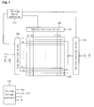
- FIG. 1 illustrates a plasma display apparatus in accordance with the invention
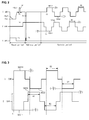
- FIG. 2 illustrates an example of a driving signal of the plasma display apparatus in accordance with the invention
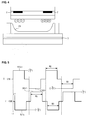
- FIG. 3 illustrates a sustain pulse of the plasma display apparatus in accordance with the invention
- FIG. 4 is a cross-sectional view of a plasma display panel
- FIG. 5 illustrates another example of a driving signal of the plasma display apparatus in accordance with the invention.
- a plasma display apparatus comprises a plasma display panel 100, a driving pulse controller 110, an address electrode driver 120, a scan electrode driver 130, a sustain electrode driver 140, and a driving voltage generator 150.
- the plasma display panel 100 comprises scan electrodes Y1 to Yn, sustain electrodes Z, and address electrodes X1 to Xm intersecting the scan electrodes Y1 to Yn and the sustain electrodes Z.
- the driving pulse controller 110 outputs a timing control signal for supplying a driving pulse by each of the address electrode driver 120, the scan electrode driver 130, and the sustain electrode driver 140.
- the address electrode driver 120 receives the timing control signal from the driving pulse controller 110, and then supplies a data pulse corresponding to a video signal to the address electrodes X1 to Xm formed in the plasma display panel 100.
- the video signal is supplied to the address electrode driver 120 through a half-toning circuit (not illustrated), a subfield mapping circuit (not illustrated), and a subfield arranging circuit (not illustrated).
- the scan electrode driver 130 receives the timing control signal from the driving pulse controller 110, and then supplies a reset pulse, a supply pulse, a scan pulse, and a sustain pulse to the scan electrodes Y1 to Yn.
- the scan electrode driver 130 supplies a sustain pulse of a first polarity to the scan electrodes Y1 to Yn at a first supply time point.
- the sustain electrode driver 140 receives the timing control signal from the driving pulse controller 110, and then supplies a bias voltage and a sustain pulse to the sustain electrodes Z.
- the sustain electrode driver 140 supplies a sustain pulse of a second polarity, which overlaps the sustain pulse of the first polarity, to the sustain electrodes Z at a second supply time point earlier than the first supply time point.
- the sustain electrode driver 140 may supply a sustain pulse of a negative polarity to overlap the sustain pulse of the positive polarity. Further, when the scan electrode driver 130 supplies a sustain pulse of a negative polarity, the sustain electrode driver 140 may supply a sustain pulse of a positive polarity to overlap the sustain pulse of the negative polarity.
- the driving voltage generator 150 generates a reset voltage -Vset, a scan voltage -Vy, sustain voltages Vs/2 and -Vs/2, a data voltage Vd, and the like.
- the reset voltage -Vset is equal to the lowest voltage of the reset pulse
- the scan voltage -Vy is equal to the lowest voltage of the scan pulse.
- the positive sustain voltage Vs/2 is equal to the highest voltage of a sustain pulse of a positive polarity
- the negative sustain voltage -Vs/2 is equal to the lowest voltage of a sustain pulse of a negative polarity.
- the scan electrode driver 130 supplies a reset pulse of a negative polarity falling from a ground level voltage GND to the reset voltage -Vset to the scan electrode Y.
- the scan electrode driver 130 supplies a reset pulse comprising a set-down pulse, which gradually falls from the negative sustain voltage -Vs/2 to the reset voltage - Vset, to the scan electrode Y.
- the address electrode driver 120 supplies a pulse of a positive polarity rising from the ground level voltage GND to a predetermined voltage V4 to the address electrode X.
- the magnitude of the predetermined voltage V4 which the address electrode driver 120 supplies during the reset period is equal to the magnitude of the data voltage Vd of the data pulse which the address electrode driver 120 supplies during an address period.
- the address electrode driver 120 can have a simple configuration.
- the scan electrode driver 130 After supplying the reset pulse, the scan electrode driver 130 supplies a supply pulse SP to the scan electrode Y.
- the address electrode driver 120 and the sustain electrode driver 140 supply the ground level voltage GND to the address electrode X and the sustain electrode Z during the supplying of the supply pulse SP, respectively.
- a predetermined amount of positive charge formed on the scan electrode Y becomes erased such that the remaining wall charges are uniform to the extent that an addressing operation can be stably performed.
- the width W1 of the supply pulse SP is, in this embodiment, smaller than the width W2 of the sustain pulse.
- the highest voltage of the supply pulse SP is substantially equal to the highest voltage of sustain pulses SUS 1+ and SUS2+ of a positive polarity.
- the scan electrode driver 130 sequentially supplies a scan pulse falling to the scan voltage -Vy to each scan electrode Y
- the address electrode driver 120 sequentially supplies a data pulse, synchronized with the scan pulse, rising to the data voltage Vd to each address electrode X. This results in the selection of a discharge cell where a sustain discharge will occur during a sustain period.
- the sustain electrode driver 140 supplies a bias voltage Vz to the sustain electrode Z during the address period such that an opposite discharge between the scan electrode Y and the address electrode X occur smoothly.
- the scan electrode driver 130 and the sustain electrode driver 140 supply the sustain pulse of the positive polarity or the negative polarity.
- the scan electrode driver 130 supplies a sustain pulse SUS1+ of a positive polarity at a first supply time point t1 of the sustain period
- the sustain electrode driver 140 supplies a sustain pulse SUS1- of a negative polarity at a second supply time point t2 earlier than the first supply time point t1.
- the sustain electrode driver 140 supplies the sustain pulse SUS1- of the negative polarity to overlap the sustain pulse SUS1+ of the positive polarity. Since the sustain pulse SUS 1+ of the positive polarity and the sustain pulse SUS1- of the negative polarity are supplied to the scan electrode Y and the sustain electrode Y, respectively, the voltage difference between the scan electrode Y and the sustain electrode Y is equal to a voltage Vs. Accordingly, the sustain discharge occurs in the discharge cell selected during the address period.
- the scan electrode driver 130 supplies a sustain pulse SUS2- of a negative polarity
- the sustain electrode driver 140 supplies a sustain pulse SUS2+ of a positive polarity during the sustain period.
- the sustain electrode driver 140 supplies the sustain pulse SUS2+ of the positive polarity to overlap the sustain pulse SUS2- of the negative polarity. Since the sustain pulse SUS2- of the negative polarity and the sustain pulse SUS2+ of the positive polarity are supplied to the scan electrode Y and the sustain electrode Y, respectively, a voltage difference between the scan electrode Y and the sustain electrode Y is equal to the voltage Vs. Accordingly, the sustain discharge occurs in the discharge cell selected during the address period.
- the supply time point of the sustain pulse SUS2+ of the positive polarity is earlier than the supply time point of the sustain pulse SUS2- of the negative polarity.
- the electric field distribution between the scan electrode Y and the sustain electrode Y is uniform.
- a sustain pulse is alternately supplied to the scan electrode or the sustain electrode
- a respective electric field is formed around the scan electrode or the sustain electrode.
- the sustain pulse of the positive polarity and the sustain pulse of the negative polarity which overlap each other, are supplied to the scan electrode Y and the sustain electrode Z, the electric field distribution between the scan electrode Y and the sustain electrode Z is uniform. This results in the generation of the stable sustain discharge.
- the sustain pulse of the negative polarity is supplied when supplying the sustain pulse of the positive polarity, the positive charges are formed on the scan electrode Y or the sustain electrode Z. Therefore, there is little likelihood that the positive charges will collide with the phosphor.
- a sustain pulse of positive polarity is supplied to the scan electrode Y and a sustain pulse of negative polarity is supplied to the sustain electrode Z, negative charges are formed on the scan electrode Y and positive charges are formed on the sustain electrode Z. Therefore, there is little likelihood that the positive charges will collide with the phosphor PH. As a result, the likelihood of damage to the phosphor decreases and a change in the return property of the phosphor is prevented.
- the phosphor becomes excited by vacuum ultraviolet radiation emitted using an inert gas and then returns to its original state, thereby emitting visible light.
- the positive charges collide with the phosphor such that the phosphor becomes degraded a property of the excitation and the return of the phosphor becomes changed. Therefore, the image quality becomes worse.
- the sustain pulse of the negative polarity is supplied when supplying the sustain pulse of the positive polarity in the embodiment, there is little likelihood that the positive charges will degrade the phosphor. This results in the prevention of the change in the return property of the phosphor.
- the amount of space charge in the discharge cell increases.
- a voltage -Vs/2 is supplied to the sustain electrode Z and the ground level voltage GND is supplied to the scan electrode Y between the start time point t2 (i.e., the second time point t2) of the supplying of the sustain pulse SUS1-of the negative polarity to the sustain electrode Z and the start time point t1 (i.e., the first time point t2) of the supplying of the sustain pulse SUS1+ of the positive polarity to the scan electrode Y.
- the amount of negative charge in a space inside the discharge cell increases. Since the sustain pulse SUS1+ of the positive polarity and the sustain pulse SUS1-of the negative polarity overlap each other after a predetermined time interval from the time point t2, the amount of charge contributing to the sustain discharge increases and the electric field distribution between the scan electrode Y and the sustain electrode Z is uniform. Accordingly, a change in the return property of the phosphor is prevented, and the efficiency of the sustain discharge increases.
- the predetermine time interval between the first supply time point t1 and the second supply time point t2 may be equal to or less than 50% of the width W2 of the sustain pulse of the positive polarity or the width W2 of the sustain pulse of the negative polarity. In such a case, the sustain discharge is stably performed, a change in the return property of the phosphor is prevented, and the efficiency of the sustain discharge increases.
- FIG. 5 illustrates another example of a driving signal of the plasma display apparatus.
- FIG. 3 illustrates that the supplying of the sustain pulses SUS1- and SUS2+ to the sustain electrode Z is performed earlier than the supplying of the sustain pulses SUS1+ and SUS2- to the scan electrode Y.
- the supplying of the sustain pulses SUS1+ and SUS2- to the scan electrode Y may be performed earlier than the supplying of the sustain pulses SUS1- and SUS2+ to the sustain electrode Z.
- FIG. 3 illustrates that the supplying of the sustain pulses SUS1- and SUS2+ to the sustain electrode Z is performed earlier than the supplying of the sustain pulses SUS1+ and SUS2- to the scan electrode Y.
- the supplying of the sustain pulses SUS1+ and SUS2- to the scan electrode Y may be performed earlier than the supplying of the sustain pulses SUS1- and SUS2+ to the sustain electrode Z.
Landscapes
- Engineering & Computer Science (AREA)
- Physics & Mathematics (AREA)
- Power Engineering (AREA)
- Plasma & Fusion (AREA)
- Computer Hardware Design (AREA)
- General Physics & Mathematics (AREA)
- Theoretical Computer Science (AREA)
- Control Of Indicators Other Than Cathode Ray Tubes (AREA)
- Control Of Gas Discharge Display Tubes (AREA)
Abstract
Description
- This invention relates to a plasma display apparatus and a method of driving the same.
- A plasma display apparatus comprises a plasma display panel in which a discharge cell is filled with a main discharge gas and an inert gas, and a driver. When a high frequency voltage is supplied to an electrode of the plasma display panel, the inert gas generates vacuum ultraviolet radiation, which thereby causes a phosphor formed between barrier ribs of the plasma display panel to emit visible light.
- The plasma display apparatus displays an image during each of subfields constituting a frame. Each of the subfields comprises a reset period for initializing all the discharge cells, an address period for selecting cells to be discharged, and a sustain period for representing gray level in accordance with the number of discharges.
- The reset period comprises a setup period and a set-down period. During the setup period, a setup pulse is supplied to scan electrodes. The setup pulse generates a weak dark discharge in the discharge cells. This results in wall charges of a positive polarity being accumulated on address electrodes and sustain electrodes, and wall charges of a negative polarity being accumulated on the scan electrodes.
- During the set-down period, a set-down pulse is supplied to the scan electrodes. As a result, a portion of the wall charges excessively accumulated on the scan electrodes is erased such that the remaining wall charges are uniform inside the discharge cells.
- During the address period, a scan pulse is supplied to the scan electrodes, and a data pulse is supplied to the address electrodes. As the voltage difference between the scan pulse and the data pulse is added to the wall voltage produced during the reset period, the cells to be discharged are selected.
- During the sustain period, a sustain pulse is supplied to the scan electrodes and the sustain electrodes. A sustain discharge occurs within the discharge cells selected during the address period, thereby displaying an image.
- The driver of the plasma display apparatus supplies a driving pulse to the electrode of the plasma display panel during the reset period, the address period and the sustain period. In other words, the driver supplies the setup pulse and the set-down pulse during the reset period, the data pulse and the scan pulse during the address period, and the sustain pulse during the sustain period.
- The present invention seeks to provide an improved plasma display apparatus and method of driving same.
- In accordance with a first aspect of the invention, a plasma display apparatus comprises a plasma display panel comprising a first electrode and a second electrode, a first electrode driver arranged to supply a first sustain pulse of a first polarity to the first electrode at a first supply time point, and a second electrode driver arranged to supply a second sustain pulse of a second polarity, which overlaps the first sustain pulse, to the second electrode at a second supply time point.
- The second supply time point may be earlier than the first supply time point.
- The plasma display apparatus may further comprise a third electrode and a third electrode driver arranged to drive the third electrode. The first electrode driver may be arranged to supply a reset pulse of a negative polarity, which falls from a first voltage to a second voltage, during a reset period, and the third electrode driver may be arranged to supply a pulse of a positive polarity, which rises from a third voltage to a fourth voltage, during the reset period.
- The fourth voltage level may be substantially equal to the highest voltage level of a data pulse, which the third electrode driver supplies during an address period.
- The reset pulse of the negative polarity may comprise a set-down pulse gradually falling to the second voltage.
- The first electrode driver may be arranged to supply a supply pulse after the first electrode driver has supplied a reset pulse falling from a first voltage to a second voltage.
- The magnitude of the highest voltage of the supply pulse may be substantially equal to the magnitude of the highest voltage of a sustain pulse.
- The polarity of the highest voltage of the supply pulse may be different from the polarity of the lowest voltage of the reset pulse.
- The width of the supply pulse may be less than the width of a sustain pulse.
- The time interval between the first supply time point and the second supply time point may be equal to or less than 50% of the width of the first sustain pulse or the width of the second sustain pulse.
- In accordance with another aspect of the invention, a method of driving a plasma display apparatus comprising a first electrode, a second electrode, and a third electrode, comprises supplying a first sustain pulse of a first polarity to the first electrode at a first supply time point, and supplying a second sustain pulse of a second polarity, which overlaps the first sustain pulse, to the second electrode at a second supply time point.
- The second supply time point may be earlier than the first supply time point.
- The method may further comprise supplying a reset pulse of a negative polarity, which falls from a first voltage to a second voltage, to the first electrode during a reset period, and supplying a pulse of a positive polarity, which rises from a third voltage to a fourth voltage, to the third electrode during the reset period.
- The fourth voltage level may be substantially equal to the highest voltage level of a data pulse supplied to the third electrode.
- The reset pulse of the negative polarity may comprise a set-down pulse gradually falling to the second voltage.
- The method may further comprise supplying a reset pulse of a negative polarity falling from a first voltage to a second voltage to the first electrode, and supplying a supply pulse to the first electrode.
- The magnitude of the highest voltage of the supply pulse may be substantially equal to the magnitude of the highest voltage of a sustain pulse.
- The polarity of the highest voltage of the supply pulse may be different from the polarity of the lowest voltage of the reset pulse.
- The width of the supply pulse may be less than the width of a sustain pulse.
- Embodiments of the invention will now be described by way of non-limiting example only, with reference to the drawings, in which
- FIG. 1 illustrates a plasma display apparatus in accordance with the invention;
- FIG. 2 illustrates an example of a driving signal of the plasma display apparatus in accordance with the invention;
- FIG. 3 illustrates a sustain pulse of the plasma display apparatus in accordance with the invention;
- FIG. 4 is a cross-sectional view of a plasma display panel; and
- FIG. 5 illustrates another example of a driving signal of the plasma display apparatus in accordance with the invention.
- As illustrated in FIG. 1, a plasma display apparatus comprises a
plasma display panel 100, adriving pulse controller 110, anaddress electrode driver 120, ascan electrode driver 130, asustain electrode driver 140, and adriving voltage generator 150. - The
plasma display panel 100 comprises scan electrodes Y1 to Yn, sustain electrodes Z, and address electrodes X1 to Xm intersecting the scan electrodes Y1 to Yn and the sustain electrodes Z. - The
driving pulse controller 110 outputs a timing control signal for supplying a driving pulse by each of theaddress electrode driver 120, thescan electrode driver 130, and thesustain electrode driver 140. - The
address electrode driver 120 receives the timing control signal from thedriving pulse controller 110, and then supplies a data pulse corresponding to a video signal to the address electrodes X1 to Xm formed in theplasma display panel 100. The video signal is supplied to theaddress electrode driver 120 through a half-toning circuit (not illustrated), a subfield mapping circuit (not illustrated), and a subfield arranging circuit (not illustrated). - The
scan electrode driver 130 receives the timing control signal from thedriving pulse controller 110, and then supplies a reset pulse, a supply pulse, a scan pulse, and a sustain pulse to the scan electrodes Y1 to Yn. In particular, thescan electrode driver 130 supplies a sustain pulse of a first polarity to the scan electrodes Y1 to Yn at a first supply time point. - The
sustain electrode driver 140 receives the timing control signal from the drivingpulse controller 110, and then supplies a bias voltage and a sustain pulse to the sustain electrodes Z. In particular, thesustain electrode driver 140 supplies a sustain pulse of a second polarity, which overlaps the sustain pulse of the first polarity, to the sustain electrodes Z at a second supply time point earlier than the first supply time point. - For example, when the
scan electrode driver 130 supplies a sustain pulse of a positive polarity, thesustain electrode driver 140 may supply a sustain pulse of a negative polarity to overlap the sustain pulse of the positive polarity. Further, when thescan electrode driver 130 supplies a sustain pulse of a negative polarity, thesustain electrode driver 140 may supply a sustain pulse of a positive polarity to overlap the sustain pulse of the negative polarity. - The following is a detailed description of operations of the
scan electrode driver 130 and thesustain electrode driver 140, with reference to FIGs. 2 and 3. - The
driving voltage generator 150 generates a reset voltage -Vset, a scan voltage -Vy, sustain voltages Vs/2 and -Vs/2, a data voltage Vd, and the like. The reset voltage -Vset is equal to the lowest voltage of the reset pulse, and the scan voltage -Vy is equal to the lowest voltage of the scan pulse. The positive sustain voltage Vs/2 is equal to the highest voltage of a sustain pulse of a positive polarity, and the negative sustain voltage -Vs/2 is equal to the lowest voltage of a sustain pulse of a negative polarity. - Operation of the embodiment of the plasma display apparatus will now be described in detail with reference to FIGs. 2 and 3.
- During a reset period, the
scan electrode driver 130 supplies a reset pulse of a negative polarity falling from a ground level voltage GND to the reset voltage -Vset to the scan electrode Y. In this exemplary embodiment, thescan electrode driver 130 supplies a reset pulse comprising a set-down pulse, which gradually falls from the negative sustain voltage -Vs/2 to the reset voltage - Vset, to the scan electrode Y. - During the reset period, the
address electrode driver 120 supplies a pulse of a positive polarity rising from the ground level voltage GND to a predetermined voltage V4 to the address electrode X. In this embodiment, the magnitude of the predetermined voltage V4 which the address electrode driver 120 supplies during the reset period is equal to the magnitude of the data voltage Vd of the data pulse which the address electrode driver 120 supplies during an address period. When the magnitude of the predetermined voltage V4 is substantially equal to the magnitude of the data voltage Vd of the data pulse, theaddress electrode driver 120 can have a simple configuration. - As above, when the reset pulse of the negative polarity and the predetermined voltage V4 are supplied during the reset period, damage to a phosphor caused by positive charges is prevented and wall charges are sufficiently formed in discharge cells of the plasma display panel.
- After supplying the reset pulse, the
scan electrode driver 130 supplies a supply pulse SP to the scan electrode Y. Theaddress electrode driver 120 and the sustainelectrode driver 140 supply the ground level voltage GND to the address electrode X and the sustain electrode Z during the supplying of the supply pulse SP, respectively. As a result, a predetermined amount of positive charge formed on the scan electrode Y becomes erased such that the remaining wall charges are uniform to the extent that an addressing operation can be stably performed. To erase the predetermined amount of positive charges, the width W1 of the supply pulse SP is, in this embodiment, smaller than the width W2 of the sustain pulse. To simplify the circuit configuration of thescan electrode driver 130, the highest voltage of the supply pulse SP is substantially equal to the highest voltage of sustainpulses SUS 1+ and SUS2+ of a positive polarity. - During the address period, the
scan electrode driver 130 sequentially supplies a scan pulse falling to the scan voltage -Vy to each scan electrode Y, and theaddress electrode driver 120 sequentially supplies a data pulse, synchronized with the scan pulse, rising to the data voltage Vd to each address electrode X. This results in the selection of a discharge cell where a sustain discharge will occur during a sustain period. The sustainelectrode driver 140 supplies a bias voltage Vz to the sustain electrode Z during the address period such that an opposite discharge between the scan electrode Y and the address electrode X occur smoothly. - After completing the addressing of the discharge cell, the
scan electrode driver 130 and the sustainelectrode driver 140 supply the sustain pulse of the positive polarity or the negative polarity. - Referring now to FIG. 3, the
scan electrode driver 130 supplies a sustain pulse SUS1+ of a positive polarity at a first supply time point t1 of the sustain period, and the sustainelectrode driver 140 supplies a sustain pulse SUS1- of a negative polarity at a second supply time point t2 earlier than the first supply time point t1. The sustainelectrode driver 140 supplies the sustain pulse SUS1- of the negative polarity to overlap the sustain pulse SUS1+ of the positive polarity. Since the sustainpulse SUS 1+ of the positive polarity and the sustain pulse SUS1- of the negative polarity are supplied to the scan electrode Y and the sustain electrode Y, respectively, the voltage difference between the scan electrode Y and the sustain electrode Y is equal to a voltage Vs. Accordingly, the sustain discharge occurs in the discharge cell selected during the address period. - The
scan electrode driver 130 supplies a sustain pulse SUS2- of a negative polarity, and the sustainelectrode driver 140 supplies a sustain pulse SUS2+ of a positive polarity during the sustain period. The sustainelectrode driver 140 supplies the sustain pulse SUS2+ of the positive polarity to overlap the sustain pulse SUS2- of the negative polarity. Since the sustain pulse SUS2- of the negative polarity and the sustain pulse SUS2+ of the positive polarity are supplied to the scan electrode Y and the sustain electrode Y, respectively, a voltage difference between the scan electrode Y and the sustain electrode Y is equal to the voltage Vs. Accordingly, the sustain discharge occurs in the discharge cell selected during the address period. The supply time point of the sustain pulse SUS2+ of the positive polarity is earlier than the supply time point of the sustain pulse SUS2- of the negative polarity. - As above, since the sustain pulse of the positive polarity and the sustain pulse of the negative polarity overlap each other, the electric field distribution between the scan electrode Y and the sustain electrode Y is uniform. In other words, when a sustain pulse is alternately supplied to the scan electrode or the sustain electrode, a respective electric field is formed around the scan electrode or the sustain electrode. On the other hand, when the sustain pulse of the positive polarity and the sustain pulse of the negative polarity, which overlap each other, are supplied to the scan electrode Y and the sustain electrode Z, the electric field distribution between the scan electrode Y and the sustain electrode Z is uniform. This results in the generation of the stable sustain discharge.
- Since the sustain pulse of the negative polarity is supplied when supplying the sustain pulse of the positive polarity, the positive charges are formed on the scan electrode Y or the sustain electrode Z. Therefore, there is little likelihood that the positive charges will collide with the phosphor. For example, as illustrated in FIG. 4, when a sustain pulse of positive polarity is supplied to the scan electrode Y and a sustain pulse of negative polarity is supplied to the sustain electrode Z, negative charges are formed on the scan electrode Y and positive charges are formed on the sustain electrode Z. Therefore, there is little likelihood that the positive charges will collide with the phosphor PH. As a result, the likelihood of damage to the phosphor decreases and a change in the return property of the phosphor is prevented. In other words, the phosphor becomes excited by vacuum ultraviolet radiation emitted using an inert gas and then returns to its original state, thereby emitting visible light. In a case where the positive charges collide with the phosphor such that the phosphor becomes degraded, a property of the excitation and the return of the phosphor becomes changed. Therefore, the image quality becomes worse. However, since the sustain pulse of the negative polarity is supplied when supplying the sustain pulse of the positive polarity in the embodiment, there is little likelihood that the positive charges will degrade the phosphor. This results in the prevention of the change in the return property of the phosphor.
- As illustrated in FIG. 3, since the supplying of the sustain pulses SUS 1- and SUS2+ to the sustain electrode Z is performed earlier than the supplying of the sustain
pulses SUS 1+ and SUS2- to the scan electrode Y, the amount of space charge in the discharge cell increases. For example, a voltage -Vs/2 is supplied to the sustain electrode Z and the ground level voltage GND is supplied to the scan electrode Y between the start time point t2 (i.e., the second time point t2) of the supplying of the sustain pulse SUS1-of the negative polarity to the sustain electrode Z and the start time point t1 (i.e., the first time point t2) of the supplying of the sustain pulse SUS1+ of the positive polarity to the scan electrode Y. Accordingly, the amount of negative charge in a space inside the discharge cell increases. Since the sustain pulse SUS1+ of the positive polarity and the sustain pulse SUS1-of the negative polarity overlap each other after a predetermined time interval from the time point t2, the amount of charge contributing to the sustain discharge increases and the electric field distribution between the scan electrode Y and the sustain electrode Z is uniform. Accordingly, a change in the return property of the phosphor is prevented, and the efficiency of the sustain discharge increases. - The predetermine time interval between the first supply time point t1 and the second supply time point t2 may be equal to or less than 50% of the width W2 of the sustain pulse of the positive polarity or the width W2 of the sustain pulse of the negative polarity. In such a case, the sustain discharge is stably performed, a change in the return property of the phosphor is prevented, and the efficiency of the sustain discharge increases.
- FIG. 5 illustrates another example of a driving signal of the plasma display apparatus. FIG. 3 illustrates that the supplying of the sustain pulses SUS1- and SUS2+ to the sustain electrode Z is performed earlier than the supplying of the sustain pulses SUS1+ and SUS2- to the scan electrode Y. However, as illustrated in FIG. 5, the supplying of the sustain pulses SUS1+ and SUS2- to the scan electrode Y may be performed earlier than the supplying of the sustain pulses SUS1- and SUS2+ to the sustain electrode Z. For example, as shown in FIG. 5, since the ground level voltage GND is supplied to the sustain electrode Z when supplying the sustain pulses SUS1+ of the positive polarity to the scan electrode Y, the amount of negative charge in a space inside the discharge cell increases. Since the sustain pulse SUS1+ of the positive polarity and the sustain pulse SUS1-of the negative polarity overlap each other after the time point t1, the amount of charge contributing to the sustain discharge increases and the electric field distribution between the scan electrode Y and the sustain electrode Z is uniform. Accordingly, a change in the return properly of the phosphor is prevented, and the efficiency of the sustain discharge increases.
- The foregoing embodiments and advantages are merely exemplary and are not to be construed as limiting the present invention. The present teaching can be readily applied to other types of apparatuses. The description of the foregoing embodiments is intended to be illustrative, and not to limit the scope of the claims. Many alternatives, modifications, and variations will be apparent to those skilled in the art.
Claims (19)
- A plasma display apparatus comprising:a plasma display panel comprising a first electrode and a second electrode;a first electrode driver arranged to supply a first sustain pulse of a first polarity to the first electrode at a first supply time point; anda second electrode driver arranged to supply a second sustain pulse of a second polarity, which overlaps the first sustain pulse, to the second electrode at a second supply time point.
- The plasma display apparatus of claim 1, wherein the second supply time point is earlier than the first supply time point.
- The plasma display apparatus of claim 1 or 2, further comprising a third electrode and a third electrode driver for driving the third electrode,
wherein the first electrode driver is arranged to supply a reset pulse of a negative polarity, which falls from a first voltage to a second voltage, during a reset period, and
the third electrode driver is arranged to supply a pulse of a positive polarity, which rises from a third voltage to a fourth voltage, during the reset period. - The plasma display apparatus of claim 3, wherein the fourth voltage level is substantially equal to the highest voltage level of a data pulse, which the third electrode driver supplies during an address period.
- The plasma display apparatus of claim 3 or 4, wherein the reset pulse of the negative polarity comprises a set-down pulse gradually falling to the second voltage.
- The plasma display apparatus of any preceding claim, wherein after the first electrode driver supplies a reset pulse falling from a first voltage to a second voltage, the first electrode driver supplies a supply pulse.
- The plasma display apparatus of claim 6, wherein the magnitude of the highest voltage of the supply pulse is substantially equal to the magnitude of the highest voltage of a sustain pulse.
- The plasma display apparatus of claim 6, wherein the polarity of the highest voltage of the supply pulse is different from the polarity of the lowest voltage of the reset pulse.
- The plasma display apparatus of any one of claims 6, 7 or 8 wherein the width of the supply pulse is less than the width of a sustain pulse.
- The plasma display apparatus of any preceding claim, wherein the time interval between the first supply time point and the second supply time point is equal to or less than 50% of the width of the first sustain pulse or the width of the second sustain pulse.
- A method of driving a plasma display apparatus comprising a first electrode, a second electrode, and a third electrode, the method comprising:supplying a first sustain pulse of a first polarity to the first electrode at a first supply time point; andsupplying a second sustain pulse of a second polarity, which overlaps the first sustain pulse, to the second electrode at a second supply time point.
- The method of claim 11, wherein the second supply time point is earlier than the first supply time point.
- The method of claim 11 or 12, further comprising supplying a reset pulse of a negative polarity, which falls from a first voltage to a second voltage, to the first electrode during a reset period; and
supplying a pulse of a positive polarity, which rises from a third voltage to a fourth voltage, to the third electrode during the reset period. - The method of claim 13, wherein the fourth voltage level is substantially equal to the highest voltage level of a data pulse supplied to the third electrode.
- The method of claim 13 or 14, wherein the reset pulse of the negative polarity comprises a set-down pulse gradually falling to the second voltage.
- The method of any one of claims 11 to 15, further comprising supplying a reset pulse of a negative polarity falling from a first voltage to a second voltage to the first electrode; and
supplying a supply pulse to the first electrode. - The method of claim 16, wherein the magnitude of the highest voltage of the supply pulse is substantially equal to the magnitude of the highest voltage of a sustain pulse.
- The method of claim 16, wherein the polarity of the highest voltage of the supply pulse is different from the polarity of the lowest voltage of the reset pulse.
- The method of any one of claims 16, 17 or 18, wherein the width of the supply pulse is less than the width of a sustain pulse.
Applications Claiming Priority (1)
| Application Number | Priority Date | Filing Date | Title |
|---|---|---|---|
| KR1020050099117A KR100830460B1 (en) | 2005-10-20 | 2005-10-20 | Driving device and driving method of plasma display panel |
Publications (1)
| Publication Number | Publication Date |
|---|---|
| EP1777679A1 true EP1777679A1 (en) | 2007-04-25 |
Family
ID=37603784
Family Applications (1)
| Application Number | Title | Priority Date | Filing Date |
|---|---|---|---|
| EP06255408A Withdrawn EP1777679A1 (en) | 2005-10-20 | 2006-10-20 | Plasma display apparatus and method of driving the same |
Country Status (5)
| Country | Link |
|---|---|
| US (1) | US20070091022A1 (en) |
| EP (1) | EP1777679A1 (en) |
| JP (1) | JP2007114787A (en) |
| KR (1) | KR100830460B1 (en) |
| CN (1) | CN1953013A (en) |
Families Citing this family (3)
| Publication number | Priority date | Publication date | Assignee | Title |
|---|---|---|---|---|
| JP5414202B2 (en) * | 2008-05-16 | 2014-02-12 | 日立コンシューマエレクトロニクス株式会社 | Plasma display device and driving circuit thereof |
| KR20100127602A (en) * | 2009-05-26 | 2010-12-06 | 엘지전자 주식회사 | Plasma display device |
| KR101373416B1 (en) * | 2012-04-18 | 2014-03-14 | 단국대학교 산학협력단 | Plasma display panel driving method |
Citations (6)
| Publication number | Priority date | Publication date | Assignee | Title |
|---|---|---|---|---|
| EP1065650A2 (en) * | 1999-06-30 | 2001-01-03 | Fujitsu Limited | Driving apparatus and method for a plasma display panel |
| US6181305B1 (en) * | 1996-11-11 | 2001-01-30 | Fujitsu Limited | Method for driving an AC type surface discharge plasma display panel |
| US20030071577A1 (en) * | 2001-10-12 | 2003-04-17 | Ji-Bin Du | Method for driving an alternating current plasma display panel and circuit therefor |
| US20050052353A1 (en) * | 2001-06-19 | 2005-03-10 | Fujitsu Hitachi Plasma Display Limited | Method of driving plasma display panel |
| US20050088376A1 (en) * | 2003-10-28 | 2005-04-28 | Matsushita Electric Industrial Co., Ltd. | Capacitive load driver and plasma display |
| US20050140581A1 (en) * | 2003-11-29 | 2005-06-30 | Kyoung-Doo Kang | Method of driving plasma display panel (PDP) |
Family Cites Families (3)
| Publication number | Priority date | Publication date | Assignee | Title |
|---|---|---|---|---|
| KR100487809B1 (en) * | 2003-01-16 | 2005-05-06 | 엘지전자 주식회사 | Plasma Display Panel and Driving Method thereof |
| KR100508252B1 (en) * | 2003-06-21 | 2005-08-18 | 엘지전자 주식회사 | Method and Apparatus for Driving Plasma Display Panel Using Selective Erasure |
| JP4860117B2 (en) * | 2004-05-21 | 2012-01-25 | 日立プラズマディスプレイ株式会社 | Display device |
-
2005
- 2005-10-20 KR KR1020050099117A patent/KR100830460B1/en not_active Expired - Fee Related
-
2006
- 2006-10-19 US US11/583,065 patent/US20070091022A1/en not_active Abandoned
- 2006-10-19 JP JP2006284658A patent/JP2007114787A/en not_active Withdrawn
- 2006-10-20 CN CNA2006101360495A patent/CN1953013A/en active Pending
- 2006-10-20 EP EP06255408A patent/EP1777679A1/en not_active Withdrawn
Patent Citations (6)
| Publication number | Priority date | Publication date | Assignee | Title |
|---|---|---|---|---|
| US6181305B1 (en) * | 1996-11-11 | 2001-01-30 | Fujitsu Limited | Method for driving an AC type surface discharge plasma display panel |
| EP1065650A2 (en) * | 1999-06-30 | 2001-01-03 | Fujitsu Limited | Driving apparatus and method for a plasma display panel |
| US20050052353A1 (en) * | 2001-06-19 | 2005-03-10 | Fujitsu Hitachi Plasma Display Limited | Method of driving plasma display panel |
| US20030071577A1 (en) * | 2001-10-12 | 2003-04-17 | Ji-Bin Du | Method for driving an alternating current plasma display panel and circuit therefor |
| US20050088376A1 (en) * | 2003-10-28 | 2005-04-28 | Matsushita Electric Industrial Co., Ltd. | Capacitive load driver and plasma display |
| US20050140581A1 (en) * | 2003-11-29 | 2005-06-30 | Kyoung-Doo Kang | Method of driving plasma display panel (PDP) |
Also Published As
| Publication number | Publication date |
|---|---|
| KR20070043162A (en) | 2007-04-25 |
| CN1953013A (en) | 2007-04-25 |
| US20070091022A1 (en) | 2007-04-26 |
| JP2007114787A (en) | 2007-05-10 |
| KR100830460B1 (en) | 2008-05-20 |
Similar Documents
| Publication | Publication Date | Title |
|---|---|---|
| JP2003302931A (en) | Method for driving plasma display panel | |
| US7551150B2 (en) | Apparatus and method for driving plasma display panel | |
| KR100667360B1 (en) | Plasma display device and driving method thereof | |
| EP1748407B1 (en) | Plasma display apparatus and driving method of the same | |
| EP1777679A1 (en) | Plasma display apparatus and method of driving the same | |
| EP1580714A2 (en) | Apparatus and method for driving plasma display panel | |
| US20060007064A1 (en) | Plasma display apparatus and driving method thereof | |
| US20070216603A1 (en) | Method of driving plasma display apparatus | |
| JP2006011459A5 (en) | ||
| JP2005250489A5 (en) | ||
| EP1804228A2 (en) | Plasma display apparatus | |
| JP5046655B2 (en) | Plasma display device | |
| KR100747269B1 (en) | Plasma display device and driving method thereof | |
| KR100658395B1 (en) | Plasma display device and driving method thereof | |
| US7619586B2 (en) | Plasma display apparatus and method for driving the same | |
| KR100761168B1 (en) | Driving Method of Plasma Display Panel | |
| KR100658343B1 (en) | Plasma display device and driving method thereof | |
| US7714808B2 (en) | Plasma display apparatus and driving method thereof | |
| KR100793292B1 (en) | Plasma display device and driving method thereof | |
| KR100658357B1 (en) | Plasma display device and driving method thereof | |
| KR100705280B1 (en) | Plasma display device and driving method thereof | |
| KR100727298B1 (en) | Plasma display device and driving method thereof | |
| KR100563072B1 (en) | Driving method and driving apparatus of plasma display panel | |
| US7733303B2 (en) | Plasma display apparatus and method of driving the same | |
| EP1939843A1 (en) | Plasma display apparatus and driving method thereof |
Legal Events
| Date | Code | Title | Description |
|---|---|---|---|
| PUAI | Public reference made under article 153(3) epc to a published international application that has entered the european phase |
Free format text: ORIGINAL CODE: 0009012 |
|
| AK | Designated contracting states |
Kind code of ref document: A1 Designated state(s): AT BE BG CH CY CZ DE DK EE ES FI FR GB GR HU IE IS IT LI LT LU LV MC NL PL PT RO SE SI SK TR |
|
| AX | Request for extension of the european patent |
Extension state: AL BA HR MK YU |
|
| 17P | Request for examination filed |
Effective date: 20071024 |
|
| AKX | Designation fees paid |
Designated state(s): DE FR GB NL |
|
| 17Q | First examination report despatched |
Effective date: 20090209 |
|
| STAA | Information on the status of an ep patent application or granted ep patent |
Free format text: STATUS: THE APPLICATION IS DEEMED TO BE WITHDRAWN |
|
| 18D | Application deemed to be withdrawn |
Effective date: 20090620 |