EP1774643B1 - Apparate und verfahren zur regelung einer elektrischen energieversorgung - Google Patents
Apparate und verfahren zur regelung einer elektrischen energieversorgung Download PDFInfo
- Publication number
- EP1774643B1 EP1774643B1 EP05760456.3A EP05760456A EP1774643B1 EP 1774643 B1 EP1774643 B1 EP 1774643B1 EP 05760456 A EP05760456 A EP 05760456A EP 1774643 B1 EP1774643 B1 EP 1774643B1
- Authority
- EP
- European Patent Office
- Prior art keywords
- waveform
- load
- amplitude
- delivered
- energy
- Prior art date
- Legal status (The legal status is an assumption and is not a legal conclusion. Google has not performed a legal analysis and makes no representation as to the accuracy of the status listed.)
- Expired - Lifetime
Links
Images





Classifications
-
- H—ELECTRICITY
- H05—ELECTRIC TECHNIQUES NOT OTHERWISE PROVIDED FOR
- H05B—ELECTRIC HEATING; ELECTRIC LIGHT SOURCES NOT OTHERWISE PROVIDED FOR; CIRCUIT ARRANGEMENTS FOR ELECTRIC LIGHT SOURCES, IN GENERAL
- H05B39/00—Circuit arrangements or apparatus for operating incandescent light sources
- H05B39/04—Controlling
- H05B39/041—Controlling the light-intensity of the source
- H05B39/044—Controlling the light-intensity of the source continuously
- H05B39/048—Controlling the light-intensity of the source continuously with reverse phase control
-
- Y—GENERAL TAGGING OF NEW TECHNOLOGICAL DEVELOPMENTS; GENERAL TAGGING OF CROSS-SECTIONAL TECHNOLOGIES SPANNING OVER SEVERAL SECTIONS OF THE IPC; TECHNICAL SUBJECTS COVERED BY FORMER USPC CROSS-REFERENCE ART COLLECTIONS [XRACs] AND DIGESTS
- Y02—TECHNOLOGIES OR APPLICATIONS FOR MITIGATION OR ADAPTATION AGAINST CLIMATE CHANGE
- Y02B—CLIMATE CHANGE MITIGATION TECHNOLOGIES RELATED TO BUILDINGS, e.g. HOUSING, HOUSE APPLIANCES OR RELATED END-USER APPLICATIONS
- Y02B20/00—Energy efficient lighting technologies, e.g. halogen lamps or gas discharge lamps
-
- Y—GENERAL TAGGING OF NEW TECHNOLOGICAL DEVELOPMENTS; GENERAL TAGGING OF CROSS-SECTIONAL TECHNOLOGIES SPANNING OVER SEVERAL SECTIONS OF THE IPC; TECHNICAL SUBJECTS COVERED BY FORMER USPC CROSS-REFERENCE ART COLLECTIONS [XRACs] AND DIGESTS
- Y10—TECHNICAL SUBJECTS COVERED BY FORMER USPC
- Y10S—TECHNICAL SUBJECTS COVERED BY FORMER USPC CROSS-REFERENCE ART COLLECTIONS [XRACs] AND DIGESTS
- Y10S315/00—Electric lamp and discharge devices: systems
- Y10S315/04—Dimming circuit for fluorescent lamps
Definitions
- the invention relates to apparatus and methods for regulating delivery of electrical energy to a load. More particularly, the invention relates to apparatus and methods for generating an integration value by integrating a signal representative of a square of an amplitude of a received electrical waveform and causing electrical energy to be delivered to the load until it has been determined that the integration value has exceeded a threshold value.
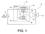
- FIG. 1 depicts a typical dimmer circuit 10 comprising a source of alternating-current (AC) power, or power supply, 12, a dimmer 14, and a load 16.
- the load 16 may be a lamp set comprising one or more lamps adapted to be connected between the hot and neutral terminals of a standard source of AC power.
- the lamp set may include one or more incandescent lamps and/or other loads such as electronic low voltage (ELV) or magnetic low voltage (MLV) loads, for example.
- EUV electronic low voltage
- MMV magnetic low voltage
- the power supply 12 supplies an AC waveform to the dimmer 14.
- the dimmer 14 regulates the delivery of electrical energy from the power supply 12 to the load 16.
- the dimmer may include a controllably conductive device 18 and a control circuit 20.
- the controllably conductive device 18 may include an input 22 adapted to be coupled to the power supply 12, an output 24 adapted to be coupled to the load 16, and a control input 26.
- the control circuit 20 may have an input 28 coupled to the input 22 of the controllably conductive device 18 and an output 30 coupled to the control input 26 of the controllably conductive device 18.
- a typical, AC, phase-control dimmer regulates the amount of energy supplied to the load 16 by conducting for some portion of each half-cycle of the AC waveform, and not conducting for the remainder of the half-cycle. Because the dimmer 14 is in series with the load 16, the longer the dimmer 14 conducts, the more energy will be delivered to the load 16. Where the load 16 is a lamp set, the more energy delivered to the load, the greater the light intensity level of the lamp set. In a typical dimming scenario, a user may adjust a control to set the light intensity level of the lamp set to a desired light intensity level. The portion of each half-cycle for which the dimmer conducts is based on the selected light intensity level.
- the controllably conductive device 18 may include a solid state switching device, which may include one or more triacs, which may be thyristors or similar control devices.
- a solid state switching device which may include one or more triacs, which may be thyristors or similar control devices.
- Conventional light dimming circuits typically use triacs to control the conduction of line current through a load, allowing a predetermined conduction time, and control the average electrical power to the light.
- One technique for controlling the average electrical power is forward phase control.
- a switching device which may include a triac, for example, is turned on at some point within each AC line voltage half cycle and remains on until the next current zero crossing.
- Forward phase control is often used to control energy to a resistive or inductive load, which may include, for example, a magnetic lighting transformer.
- a power-switching device such as a field effect transistor (FET), a MOSFET (metal oxide semiconductor FET), or an insulated gate bipolar transistor (IGBT), for example, may be used for each half cycle of AC line input when turn-off phase is to be selectable.
- FET field effect transistor
- MOSFET metal oxide semiconductor FET
- IGBT insulated gate bipolar transistor
- reverse phase control the switch is turned on at a voltage zero crossing of the AC line voltage and turned off at some point within each half cycle of the AC line current. A zero-crossing is defined as the time at which the voltage equals zero at the beginning of each half-cycle.
- Reverse phase control is often used to control energy to a capacitive load, which may include for example, an electronic transformer connected low voltage lamp.
- the switching device may have a control or "gate” input 26 that is connected to a gate drive circuit, such as an FET drive circuit, for example. Control inputs on the gate input render the switching device conductive or non-conductive, which in turn controls the energy supplied to the load.
- FET drive circuitry typically provides control inputs to the switching device in response to command signals from a microcontroller. FET protection circuitry may also be provided. Such circuitry is well known and need not be described herein.
- the microcontroller may be any processing device such as a programmable logic device (PLD), a microprocessor, or an application specific integrated circuit (ASIC), for example. Power to the microcontroller may be supplied by a power supply.
- a memory such as an EEPROM, for example, may also be provided.
- Inputs to the microcontroller may be received from a zero-crossing detector.
- the zero-crossing detector determines the zero-crossing points of the input AC waveform from the AC power supply 12.
- the microcontroller sets up gate control signals to operate the switching device to provide voltage from the AC power supply 12 to the load 16 at predetermined times relative to the zero-crossing points of the AC waveform.
- the zero-crossing detector may be a conventional zero-crossing detector, and need not be described here in further detail.
- the timing of transition firing pulses relative to the zero crossings of the AC waveform is also known, and need not be described further.
- FIGs. 2A and 2B depict example prior-art dimmed waveforms. Shown in FIG. 2A is a single-frequency AC waveform having an amplitude profile v 1 (t) during a first half-cycle T H and an amplitude profile v 2 (t) during a second half-cycle T H .
- the absolute value of peak amplitude during each half cycle is A.
- the AC waveform delivered to the dimmer is the same for both half-cycles. Because the dimmer conducts for the same amount of time, t c , each half-cycle, t H , the amount of energy delivered to the load during the second half-cycle will be the same as the amount of energy delivered during the first half-cycle. Though this is usually acceptable, amplitude changes in the AC waveform may cause fluctuations in the amount of energy actually delivered to the load from half-cycle to half-cycle ( e.g ., the light level may fluctuate).
- Shown in FIG. 2B is a single-frequency AC waveform having an amplitude profile v 1 (t) during a first half-cycle T H and an amplitude profile v 2 (t) during a second half-cycle T H , wherein the absolute value of peak amplitude during the first half cycle is A 1 and the absolute value of peak amplitude during the second half cycle is A 2 .
- the absolute value of peak amplitude, A 2 of the waveform during the second half-cycle is different from ( e.g ., lower than) the absolute value of peak amplitude, A 1 , during the first half-cycle.
- the amount of energy delivered to the load during second half-cycle is different from ( e.g ., less than) the amount of energy delivered to the load during the first half-cycle.
- T H the root-mean-square voltage delivered to the load will change as the amplitude of the AC waveform changes.
- other loads may be driven from the same power source that drives the lighting.
- a ship's engines may be driven by the same power source that drives the ship's lighting.
- the voltage waveform delivered to the lighting is often corrupted.
- the waveform varies wildly between one half-cycle and the next.
- DE 4406371 discloses a procedure for controlling the brightness of lamps, which uses a semiconducting rectifier bridge circuit in series with the lamp.
- the rectifier is switched on at the zero-crossing point of the incoming voltage wave and remains conducting until the output voltage of an integrator exceeds a chosen threshold.
- the input voltage to the integrator comes from a squaring circuit which in turn is fed with a voltage proportional to the current flowing through the rectifier.
- the integrator is reset at every zero crossing.
- the invention provides apparatus and methods for regulating delivery of electrical energy to a load.
- electrical energy is delivered to the load until it has been determined that the threshold amount of energy has been delivered. Once it has been determined that the threshold amount of energy has been delivered to the load, the delivery of electrical energy is discontinued.
- the invention may be embodied in hardware, software, or a combination of hardware and software.
- a dimmer for regulating the delivery of electrical energy from a source of electrical energy to a lighting load
- the dimmer comprising: a controllably conductive device including an input adapted to be coupled to the source of electrical energy, an output adapted to be coupled to the load, and a control input; and a control circuit having an input coupled to either the input or the output of the controllably conductive device and an output coupled to the control input of the controllably conductive device, wherein the control circuit is operable to sample an electrical waveform at a sampling rate to produce a sampled waveform, the sampling rate chosen such that the human eye cannot discern light fluctuations of the lighting load due to the sampling rate; generate an integration value by integrating a signal representative of a square of the sampled waveform; determine whether the integration value has exceeded a threshold value; and cause electrical energy to be delivered to the load until it has been determined that the integration value has exceeded the threshold value.
- a method for regulating the delivery of electrical energy to a lighting load comprising: sampling an electrical waveform at a sampling rate to produce a sampled waveform, the sampling rate chosen such that the human eye cannot discern light fluctuations of the lighting load due to the sampling rate; generating an integration value representative of an integral of a square of the sampled waveform; determining from the integration value whether a threshold amount of electrical energy has been delivered to the load; and causing electrical energy to be delivered to the load at least until it has been determined that the threshold amount of energy has been delivered to the load.
- An example embodiment of a control circuit may include a rectifier, a first comparator, a sawtooth wave generator, an integrator, a second comparator, and a drive circuit.
- the rectifier generates a rectified waveform having an amplitude representative of the absolute value of the amplitude of the alternating-current waveform.
- the first comparator receives the rectified waveform and a sawtooth waveform, and outputs a voltage-square pulse train based on a comparison of the rectified waveform and the sawtooth waveform.
- the integrator generates an integration signal based on the voltage-square pulse train.
- the integration signal is representative of the integral of the square of the alternating-current waveform.
- the second comparator outputs a control signal based on a comparison of the integration signal and a threshold value.
- the drive circuit regulates delivery of electrical energy to the load based on the control signal. If the amplitude of the integration signal exceeds the threshold, the drive circuit causes the delivery of electrical energy to be discontinued.
- the impedance of the load may be considered constant at steady-state (i.e., after the filament of the lamp has been heated to a steady-state temperature).
- the integral of v 2 (t) is representative of the energy delivered to the load, as R is constant.
- the integral of v 2 (t) is also representative of the average power delivered to the load, as R and t H are constant.
- the amount of energy delivered to the load may be regulated by integrating v 2 (t) over time, and comparing the integrated value to a threshold value.
- the threshold value may be chosen such that the integral of v 2 (t) reaches the threshold value when a desired amount of energy has been delivered to the load.
- FIG. 3 depicts a method according to the invention for regulating delivery of electrical energy to a load.
- the input to the process is an unregulated AC waveform at 26.
- the input waveform is scaled down and full-wave rectified at 28.
- a representation of the square of the input waveform is produced, wherein the representation may simply be the square of the input waveform.
- a representation of the integral of the square of the input waveform is produced, wherein this representation may simply be computed by integrating the representation of the square of the input waveform.
- the result of 32 is representative of the energy delivered to the load so far in the current half-cycle, and is compared to a threshold level that that corresponds to a desired intensity level of the load at 34.
- the power-switching device is driven according to the comparison between the threshold and the result of the integral. That is, energy is delivered to the load until the result of the integral reaches the threshold. After the threshold is reached, energy delivery is discontinued for that half-cycle. The process is complete at 38 and repeats for every half cycle.
- Such a method may be implemented in hardware or software, or in a combination of hardware and software. Such a system may be employed in connection with an electronic dimmer. One or more electrical circuits may be used to perform the functions described. The methods of the invention may be implemented as one or more computer programs in one or more microprocessors.
- FIG. 4 is a functional block diagram of an example embodiment of a system 100 according to the invention for regulating electrical energy delivered to a load.
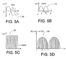
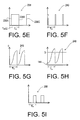
- FIGs. 5A-I depict waveforms at various points in the functional block diagram of FIG 4 .
- An input AC waveform 205 is provided to a full-wave rectifier 110.
- the input AC waveform 205 may be represented as a sine wave having a constant frequency, f, and a voltage amplitude, v(t), as shown in FIG. 5A .
- the period, T H , of a half-cycle of the sine wave is 1/2f.
- a zero crossing, Z, occurs at the beginning and end of every half-cycle.
- the full-wave rectifier 110 outputs a rectified voltage waveform 215 shown in FIG. 5B .
- the output of the full-wave rectifier 110 (rectified voltage waveform 215) is provided to a pulsed waveform generator 130.
- a sawtooth generator 120 provides a sawtooth waveform 225 (shown in FIG. 5C ) to the pulsed wave generator 130. If the amplitude, v r (t), of the rectified voltage waveform 215 is greater than the amplitude of the sawtooth waveform 225, then the pulsed waveform generator 130 outputs a signal having the amplitude of the rectified voltage waveform 215. If the amplitude, v r (t), of the rectified voltage waveform 215 is less than the amplitude of the sawtooth waveform 225, then the pulsed waveform generator 130 outputs a signal having a relatively low (logical zero) amplitude. Thus, the pulsed waveform generator 130 generates a pulsed waveform 235 (shown in FIG.
- the width of a pulse of pulsed waveform 235 is the width of a pulse of pulsed waveform 235
- T is the period of the sawtooth waveform 225.
- V pw ⁇ ⁇ v 2 t
- V pw the average voltage of the pulsed waveform 235.
- the pulsed waveform 235 is representative of the square of the amplitude of the input AC waveform 205.
- the area under the curve of pulsed waveform 235 is proportional to the area under the curve of the square of the amplitude v(t) of the input AC waveform 205.
- the integrator 140 receives the pulsed waveform 235 as well as a zero-cross pulse waveform 240 (shown in FIG. 5F ).
- the zero-cross pulse waveform 240 is produced by a microcontroller 160 in response to a zero-cross square waveform 238 (shown in FIG. 5E ) produced by a zero-cross detector 137.
- the zero-cross pulse waveform 240 is a train of pulses that may be used by the integrator 140 to reset the integration process at the beginning of each half-cycle.
- the zero-cross pulse waveform 240 has a frequency of approximately two times the frequency of the input AC waveform 205 ( e.g., 120 Hz). Each pulse of the zero-cross pulse waveform 240 corresponds to a zero-crossing of the input AC waveform 205.
- the zero-cross square waveform 238 produced by the zero-cross detector 137 has a leading edge (rising edge) 238A that corresponds to the first zero-crossing (from negative to positive half cycle) of the input AC waveform 205; a trailing edge (falling edge) 238B corresponds to the next zero-crossing (from positive to negative half cycle); the next leading edge 238C corresponds to the next zero-crossing, and so on.
- the zero-cross square waveform 238 has a frequency approximately equal to the frequency of the input AC waveform 205 ( e.g., 60 Hz) and a duty cycle of about 50%.
- the microprocessor 160 is configured to detect the leading and trailing edges of the zero-cross square waveform 238 and to produce the zero-cross pulse waveform 240 in response. Note that the leading and trailing edges of the zero-cross square waveform 238 are delayed slightly by a time T delay from the actual zero-crossing times of the input AC waveform 205 due to an inherent time delay in the circuitry of the zero-crossing detector 137. The microcontroller 160 compensates for this delay and generates the zero-cross pulse waveform 240 having pulses that occur at the actual zero-crossing times of the input AC waveform 205.
- the zero-crossing detector 137 provides accurate and reliable detection of the zero crossings Z of the input AC waveform 205 using the technology described in U.S. Patent Nos. 6,091,205 and 6,380,692 , both entitled "Phase controlled dimming system with active filter for preventing flickering and undesired intensity changes.”
- the zero-crossing detector 137 has an active filter for recovering the AC fundamental waveform from the input AC waveform 205 and provides zero-crossing indications of the AC fundamental waveform.
- the recovered AC fundamental is substantially free of noise or distortion, and of frequency components greater than at least second order harmonics, that may be present on the AC line voltage waveform, and that might otherwise result in faulty or incorrect zero crossing detection.
- the integration waveform 245 (the output of the integrator 140) is shown in FIG. 5G .
- the integrator 140 resets itself as described above based on the zero-cross pulse waveform 240 from the microcontroller 160.
- the amplitude of the sawtooth waveform 225 may be greater than the largest expected amplitude of the input AC waveform 205, and the frequency of the sawtooth waveform 215 much higher than the frequency of the input AC waveform 205 to eliminate any noticeable jitter in the integrator output. Furthermore, because it is known that the human eye cannot readily discern lighting fluctuations of less than about 20 ⁇ sec, it is desirable that the period of the sawtooth wave be less than about 20 ⁇ sec ( i.e., that the frequency of the sawtooth wave exceed 50 kHz). In this way, the threshold value will be reached within 20 ⁇ sec of the time that the threshold amount of energy has been delivered to the load.
- the frequency of the input AC waveform 205 may be 50 or 60 Hz
- the frequency of the sawtooth waveform 225 may be about 80-110 kHz.
- the amplitude of the input AC waveform 205 may be brought down from about 120 V to about 4-5 V before it is introduced into the voltage regulation circuit
- the amplitude of the sawtooth waveform 225 may be about 6 V.
- a small DC offset voltage 144 is added to the output of the integrator 140 to produce an offset integration waveform 248 (shown in FIG. 5H ).
- the offset integration waveform 248 is then provided to a comparator 150.
- the small DC offset voltage 144 lifts the integration waveform 245 away from zero, which avoids errors that could occur at the comparator 150 when the integration waveform 245 is low in amplitude.
- the comparator 150 compares the level of the offset integration signal 248 out of adder 142 to a pre-selected threshold level D (shown in FIG. 5H ) that indicates when to stop delivering electrical energy to the load.
- the pre-selected threshold level D is produced by the threshold generator 147 based on the duty cycle of a pulse-width modulated (PWM) signal provided by a microcontroller 160.
- PWM pulse-width modulated
- the pre-selected threshold level D could instead be set by a potentiometer or other means not dependent on the microcontroller 160.
- the pre-selected threshold level D may be expressed as a percentage, and may be based on a desired intensity level associated with the load.
- the amplitude of the offset integration waveform 248 is delivered to the load until it has been determined that the amplitude of the offset integration waveform 248 has reached the threshold D (i.e., that a threshold amount of energy has been delivered to the load).
- the amplitude of the offset integration waveform 248 reaches the threshold D, the delivery of electrical energy to the load is discontinued.
- the threshold D may be expressed as the amount of energy needed to illuminate the light set at the desired intensity level.
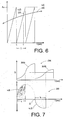
- both half-cycles of the AC waveform have the same amplitude profile. Consequently, for each half-cycle, the threshold D, shown in FIG. 5H , is reached after the same amount of time from the zero-crossing at the beginning of the half-cycle. Accordingly, in a dimming system supplied with a waveform as shown in FIG. 5B , a dimmer conducting for the same amount of time each half-cycle would deliver about the same amount of electrical energy each half-cycle. Conversely, in a dimming system according to the invention, the threshold D would be reached after about the same amount of time into each half-cycle of such a waveform.
- FIG. 7 depicts an example dimmed waveform 260 in accordance with the invention, wherein the amplitude profile of the dimmed waveform 260 varies from half-cycle to half-cycle.
- the controllably conductive device 18 receives the input AC waveform 205 and outputs the dimmed waveform 260.
- the solid line represents the energy level that is actually delivered to the dimmed load 16
- the dotted line represents the portion of the input AC waveform 205 that is not delivered to the load.
- the dimmed waveform 260 has a voltage amplitude, v I (t), and current is delivered to the load for an amount of time t I . Note that current is delivered during the first half-cycle until the amplitude of the offset integration waveform 264 exceeds the threshold level D. Thereafter, the current is gated off, and the delivery of current is discontinued.
- the waveform 260 has a voltage amplitude v II (t) that is relatively low compared to the amplitude v I (t) of the waveform during the first half-cycle. Consequently, during the second half-cycle, current is delivered to the load for an amount of time t II that is longer than t I . The amount of energy delivered to the load, however, is the same for both half-cycles. Note again that current is delivered during the second half-cycle until the amplitude of the integral waveform 264 exceeds the threshold level D. Thereafter, the current is gated off, and the delivery of current is discontinued.
- the input 28 of the control circuit 20 is connected to the input 22 of the controllably conductive device 18 and receives the input AC waveform 205.
- the integration continues the entire length of each half-cycle as shown by the offset integration waveform 264 in FIG. 7 .
- the input 28 of the control circuit 20 could alternatively be connected to the output 24 of the controllably conductive device 18 to achieve the same results.
- v 2 (t) will reflect fluctuations in the amplitude of the input AC waveform by reaching the threshold value sooner or later, depending on whether the amplitude fluctuations caused net energy increases or decreases, respectively.
- the comparator 150 outputs a control signal 255 (shown in FIG. 5I ) having an amplitude indicative of the comparison of the offset integration signal 248 and the threshold D.
- the comparator 150 may be configured such that the control signal 255 is a relatively low-voltage signal if the level of the signal out of the integrator is below the threshold, and a relatively high-voltage signal if the level of the signal out of the integrator exceeds the threshold.
- the microcontroller 160 receives the control signal 255 out of the comparator 150 and drives the switching device 170 that causes electrical energy to be delivered to the load as long as the control signal 255 is low.
- the microcontroller 160 does not cause electrical energy to be delivered to the load when the control signal 255 is high.
- electrical energy is delivered to the load as long as the offset integration signal 248 is below the threshold D.
- electrical energy is delivered to the load until it is determined that the threshold amount of energy has been delivered to the load during the half-cycle. Consequently, roughly the same amount of energy is delivered to the load each half-cycle.
- the microcontroller 160 is used in the described embodiment to control the operation of the switching device 170, other control circuits could be used here to drive the switching device 170.
- the microcontroller 160 will not discontinue causing energy to be delivered to the load during that half-cycle, and less than the threshold amount of energy will be delivered to the load during that half-cycle.
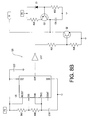
- FIGs. 8A-E depict schematic diagrams of an example embodiment of the functional block diagram of FIG 4 .
- the microcontroller 160 may interface with the circuitry of FIGs. 8A-E and provide to the switching device 170 drive signals that control the amount of current delivered to the load.
- FIG. 8A shows an example embodiment of the full-wave rectifier 110.
- the input waveform 205 is provided at the HOT and NEUTRAL terminals. Circuit common for the entire schematic is referenced to the HOT terminal.
- the input waveform 205 may be scaled down to an acceptable level (preferably about 4.7 volts peak) for the integrated circuits (ICs) in the following stages using resistors R101, R102, and R103. To achieve such a level, resistors R101 and R102 may be 220k ⁇ resistors and resistor R103 may be a 12.4k ⁇ resistor.
- the scaled signal may be fed into a voltage follower including an operational amplifier (“op amp”) U4:A, which may be an LM224DT, for example, to provide a buffer between the line voltage input AC waveform 205 and the rest of the circuitry.
- the output of the voltage follower may be rectified using an active full-wave rectifier, including op amps U4:B and U4:C, a dual diode U11, such as a BAV70, and resistors R28 and R29, which may be 100k ⁇ resistors.
- the output of the full-wave rectifier 110 (at node A) is the rectified voltage waveform 215 (in FIG. 5A ).
- Capacitors C13 and C 14, which may be 0.1 ⁇ F capacitors, may be provided to guard against undesirable noise from the power supplies P1 and P2, which may be ⁇ 12V power supplies.
- FIG. 8B shows an example embodiment of the sawtooth generator 120.
- a 555 timer U5 which may be an MC1455B, generates a square wave, having a frequency of approximately 105kHz and a duty cycle of 95%.
- the frequency and duty cycle of the square wave are set by the values of resistors R40 and R41, and capacitor C19, which may be 680 ⁇ , 12.4k ⁇ , and 1000pF, respectively.
- the output of the 555 timer U5 is inverted using inverter U7:F, which may be an MC74AC14, to obtain a square wave having the same frequency and a 5% duty cycle.
- a constant current source is provided, via power supply P4, which may be a 12 V power supply, using transistor Q3, which may be a 2N3906, a 3.9k ⁇ resistor R20, a 3.3V zener diode Z1, and a 220k ⁇ resistor R22, to charge capacitor C8 at a constant dv/dt rate (of approximately 667kV/sec).
- the inverted square wave pulses the base of a transistor Q2, which may be an MPSA06, once every 9.6 ⁇ sec. Whenever the base of transistor Q2 is high, current flows from the collector to the emitter of transistor Q2 discharging capacitor C8, which may be a 1000 pF capacitor.
- the combination of the constant dv/dt charging and pulsed discharging of C8 provides the sawtooth waveform 225 (in FIG. 5C ) at node B.
- the sawtooth waveform 225 may have an amplitude of approximately 6.4 volts.
- a capacitor C22 which may be a 0.1 ⁇ F capacitor, may be provided to guard against undesirable noise from the power supply P3, which may be a 5V power supply.
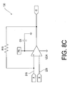
- FIG. 8C shows an example embodiment of the pulsed waveform generator 130.
- the output of the full-wave rectifier 110 may be provided to the positive input of a comparator U2:A, which may be an LM2903D.
- the output of the sawtooth generator 120 may be provided to the negative input of comparator U2:A.
- the comparator U2:A When the output of the rectified voltage waveform 215 is less than the output of the sawtooth waveform 225, then the comparator U2:A outputs a "low" signal (logical zero).
- the comparator U2:A When the output of the rectified voltage waveform 215 is greater than the output of the sawtooth waveform 225, then the comparator U2:A outputs a "high" signal, which may be pulled up to the amplitude of the rectified voltage waveform 215 through a resistor R19, which may be a 4.75k ⁇ resistor. Thus, the comparator U2:A may generate the pulsed waveform 235 (shown in FIG. 5D ) at node C that has a peak amplitude that follows the peak amplitude of the rectified voltage waveform 215 and a duty cycle, D(t), that varies as the amplitude of the rectified voltage waveform 215.
- a capacitor C4 which may be a 0.1 ⁇ F capacitor, may be provided to guard against undesirable noise from the power supply P4, which may be a 12V power supply.
- FIG. 8D shows an example embodiment of the integrator 140.
- the output of the op amp integrator is sent to an inverting amplifier stage (including LM224DT op amp U1:D, 10k ⁇ resistor R6, and 47k ⁇ resistor R8).
- the signal at the output of the inverting amplifier stage is positive and of greater amplitude than the output of the op amp integrator.
- the node ZERO_X RST (or Zero-Cross Reset) provides the zero-cross pulse waveform 240 (shown in FIG. 5F ).
- FIG. 8E shows an example embodiment of the threshold generator 147, DC voltage offset 144, adder 142, and comparator 150.
- the node THRESHOLD provides a pulse-width modulated (PWM) signal from the microcontroller 160.
- PWM pulse-width modulated
- the duty cycle of the PWM signal is controlled by the microcontroller 160.
- the PWM signal is filtered using a three-stage low-pass filter (including 10k ⁇ resistors R31, R36, and R37, and 0.022 ⁇ F capacitors C15, C16, and C17), which provides a DC (direct current) voltage level that can be altered by changing the duty cycle of the PWM signal.
- the filtered voltage at the positive input of LM224DT op amp U4:D is amplified by a non-inverting amplifier (including LM224DT op amp U4:D, and 22k ⁇ resistors R33 and R34), thus providing the threshold D as shown in FIG. 5G .
- a small DC voltage offset is produced by LM224DT op amp U1:C, 100k ⁇ resistor R1, and 2.2k ⁇ resistor R2.
- This small DC voltage offset is added to the integration waveform 245 using LM224DT op amp U1:B and 100k ⁇ resistors R4 and R5 to produce the offset integration waveform 248 (shown in FIG. 5G ).
- the offset integration waveform 248 is compared to the threshold D using an LM2903D comparator U2:B, such that the output of the comparator U2:B goes "high" when the offset integration waveform 248 is greater than the threshold D, producing control signal 255 (in FIG. 5H ).
- the control signal 255 is provided to the microcontroller at node MICRO_DRIVE.
- the microcontroller 160 may use the control signal 255 to determine when to turn off the switching device 170 that controls the amount of current delivered to the load.
- FIG. 9 is a functional block diagram of a system 300 for regulating delivery of electrical energy to a load according to a second embodiment of the invention.
- the second embodiment may include a multiplier integrated circuit (IC) 330, such as a four-quadrant analog multiplier (part number AD633), manufactured by Analog Devices, Inc.
- the rectified waveform 215 may be provided to each of two positive signal inputs of the multiplier IC 330 in order to produce the square of the rectified voltage waveform 215.
- the square of the rectified voltage waveform 215 may then be provided to the input of the integrator 140.
- the other blocks of FIG. 9 operate as discussed above.
- the input signal may be provided directly to the microcontroller.
- the input signal may be preconditioned to ensure that the signal is acceptable to the microcontroller.
- the microcontroller may then be programmed to square the waveform and perform the other functions described above.
- FIG. 10 is a functional block diagram of a system 400 for regulating delivery of electrical energy to a load according to a third embodiment of the invention.
- the third embodiment most of the steps of the method for regulating delivery of electrical energy to a load are executed by software in the microcontroller 410.
- the microcontroller 410 simply receives the rectified waveform 215 and the zero-cross square waveform 238 from zero-crossing detector 137 and outputs the drive signal to control the switching device 170.
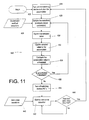
- FIG. 11 shows the algorithm 420 running in microcontroller 410 for regulating electrical energy delivered to a load according to the third embodiment of the invention.
- the algorithm 420 begins at 422.
- the microcontroller outputs a signal to turn on the switching device 170 and an accumulator (used during the algorithm) is cleared.
- the rectified voltage waveform 215 is input to the microcontroller at 426 and sampled at 428.
- the sampled value is squared at 430 and added to the accumulator at 432.
- the value of the accumulator is compared to a threshold value that is representative of the amount of energy to be delivered to the load.
- the algorithm records another sample of the rectified voltage waveform 215 at 428. Preferably, the sampling occurs every 10 ⁇ sec. If the accumulator has exceeded the threshold at 436, the microcontroller then outputs a signal to turn off the switching device 170 at 438. At 442, the microcontroller waits for the next zero-cross detection, provided at 440. At 444, if the next zero-cross has not been detected, the microcontroller continues to wait at 442. Otherwise, the microcontroller repeats the process beginning with turning on the switching device 170 and clearing the accumulator at 424.
Landscapes
- Circuit Arrangement For Electric Light Sources In General (AREA)
- Circuit Arrangements For Discharge Lamps (AREA)
- Ac-Ac Conversion (AREA)
- Charge And Discharge Circuits For Batteries Or The Like (AREA)
Claims (18)
- Dimmer (14) zum Regulieren der Zuführung von elektrischer Energie von einer Quelle (12) von elektrischer Energie zu einer Beleuchtungslast (16), wobei der Dimmer Folgendes umfasst:eine steuerbar leitende Vorrichtung (18) mit einem Eingang (22) zum Koppeln mit der Quelle von elektrischer Energie, einem Ausgang (24) zum Koppeln mit der Last und einem Steuereingang (26); undeine Steuerschaltung (20) mit einem Eingang (28), der entweder mit dem Eingang oder dem Ausgang der steuerbar leitenden Vorrichtung gekoppelt ist, und einem Ausgang (30), der mit dem Steuereingang der steuerbar leitenden Vorrichtung gekoppelt ist,dadurch gekennzeichnet, dass die Steuerschaltung die folgenden Aufgaben hat:Abtasten einer elektrischen Wellenform mit einer Abtastrate zum Erzeugen einer abgetasteten Wellenform, wobei die Abtastrate so gewählt wird, dass das menschliche Auge keine Lichtschwankungen der Beleuchtungslast aufgrund der Abtastrate wahrnehmen kann;Erzeugen (32) eines Integrationswertes durch Integrieren eines Signals, das für ein Quadrat der abgetasteten Wellenform repräsentativ ist;Ermitteln (34), ob der Integrationswert einen Schwellenwert überschritten hat; undBewirken (36), dass elektrische Energie der Last zugeführt wird, bis festgestellt wurde, dass der Integrationswert den Schwellenwert überschritten hat.
- Dimmer (14) nach Anspruch 1, wobei die Steuerschaltung (20) ferner die Aufgabe hat zu bewirken, dass die Zuführung von elektrischer Energie zu der Last (16) unterbrochen wird, auf der Basis einer Feststellung, dass die integrierte Spannung den Schwellenwert überschritten hat.
- Dimmer (14) nach Anspruch 1, wobei der Schwellenwert auf einer mit der Last (16) assoziierten Lichtintensität basiert.
- Dimmer (14) nach Anspruch 1, wobei die elektrische Wellenform eine Wechselstromwellenform ist.
- Dimmer (14) nach Anspruch 4, wobei der Schwellenwert eine der Last während eines Halbzyklus der Wechselstromwellenform zuzuführende Energiemenge repräsentiert.
- Dimmer (14) nach Anspruch 4, wobei die Steuerschaltung (20) ferner die Aufgabe hat, einen Nulldurchgang der Wechselstromwellenform zu identifizieren und den Integrationswert für eine Zeitdauer beginnend beim Nulldurchgang zu berechnen.
- Dimmer (14) nach Anspruch 1, wobei die pulsierte Wellenform ein Tastverhältnis hat, das in Abhängigkeit von der Amplitude der elektrischen Wellenform variiert.
- Dimmer (14) nach Anspruch 1, wobei die gepulste Wellenform eine Folge von Pulsen umfasst, wobei jeder genannte Impuls eine Pulsbreite und eine Pulsamplitude auf der Basis einer momentanen Amplitude der elektrischen Wellenform hat.
- Dimmer (14) nach Anspruch 8, wobei jeder genannte Puls eine Pulsbreite und eine Pulsamplitude auf der Basis eines Vergleichs zwischen einer Sägezahnwellenform und einer Wellenform mit einer Amplitude hat, die den absoluten Wert der Amplitude der elektrischen Wellenform repräsentiert.
- Verfahren zum Regulieren der Zuführung von elektrischer Energie zu einer Beleuchtungslast (16), wobei das Verfahren Folgendes beinhaltet:Abtasten einer elektrischen Wellenform mit einer Abtastrate zum Erzeugen einer abgetasteten Wellenform, wobei die Abtastrate so gewählt ist, dass das menschliche Auge keine Lichtschwankungen der Beleuchtungslast aufgrund der Abtastrate wahrnehmen kann;Erzeugen (32) eines Integrationswertes, der für ein Integral eines Quadrats der abgetasteten Wellenform repräsentativ ist;Ermitteln (32) anhand des Integrationswertes, ob der Last ein Schwellenbetrag von elektrischer Energie zugeführt wurde; undBewirken (36), dass der Last elektrische Energie zugeführt wird, wenigstens bis festgestellt wurde, dass der Last der Schwellenbetrag von Energie zugeführt wurde.
- Verfahren nach Anspruch 10, das Folgendes beinhaltet:Bewirken, dass die Zuführung von elektrischer Energie zur Last (16) unterbrochen wird, auf der Basis einer Feststellung, dass der Last der Schwellenbetrag von Energie zugeführt wurde.
- Verfahren nach Anspruch 10, wobei der Schwellenwert auf einer mit der Last (16) assoziierten Lichtintensität basiert.
- Verfahren nach Anspruch 10, wobei die elektrische Wellenform eine Wechselstromwellenform ist.
- Verfahren nach Anspruch 13, wobei der Schwellenbetrag von Energie eine der Last (16) während eines Halbzyklus der Wechselstromwellenform zuzuführende Energiemenge ist.
- Verfahren nach Anspruch 13, das Folgendes beinhaltet:Identifizieren eines Nulldurchgangs der Wechselstromwellenform; undErzeugen des Integrationswertes für eine Zeitdauer beginnend mit dem Nulldurchgang.
- Verfahren nach Anspruch 10, wobei die gepulste Wellenform ein Tastverhältnis hat, das in Abhängigkeit von der Amplitude der elektrischen Wellenform variiert.
- Verfahren nach Anspruch 10, wobei die gepulste Wellenform eine Sequenz von Pulsen umfasst, wobei jeder genannte Puls eine Pulsbreite und eine Pulsamplitude auf der Basis einer momentanen Amplitude der elektrischen Wellenform hat.
- Verfahren nach Anspruch 17, wobei jeder genannte Puls eine Pulsbreite und eine Pulsamplitude auf der Basis eines Vergleichs zwischen einer Sägezahnwellenform und einer Wellenform mit einer Amplitude hat, die für den Absolutwert der Amplitude der empfangenen elektrischen Wellenform repräsentativ ist.
Applications Claiming Priority (2)
| Application Number | Priority Date | Filing Date | Title |
|---|---|---|---|
| US10/865,083 US7259524B2 (en) | 2004-06-10 | 2004-06-10 | Apparatus and methods for regulating delivery of electrical energy |
| PCT/US2005/020595 WO2005124986A1 (en) | 2004-06-10 | 2005-06-10 | Apparatus and methods for regulating delivery of electrical energy |
Publications (2)
| Publication Number | Publication Date |
|---|---|
| EP1774643A1 EP1774643A1 (de) | 2007-04-18 |
| EP1774643B1 true EP1774643B1 (de) | 2015-12-09 |
Family
ID=34972451
Family Applications (1)
| Application Number | Title | Priority Date | Filing Date |
|---|---|---|---|
| EP05760456.3A Expired - Lifetime EP1774643B1 (de) | 2004-06-10 | 2005-06-10 | Apparate und verfahren zur regelung einer elektrischen energieversorgung |
Country Status (10)
| Country | Link |
|---|---|
| US (1) | US7259524B2 (de) |
| EP (1) | EP1774643B1 (de) |
| JP (1) | JP2008503069A (de) |
| CN (1) | CN1981425B (de) |
| AU (1) | AU2005255920B2 (de) |
| BR (1) | BRPI0512008A (de) |
| CA (1) | CA2569996C (de) |
| IL (1) | IL179860A (de) |
| MX (1) | MXPA06014428A (de) |
| WO (1) | WO2005124986A1 (de) |
Families Citing this family (131)
| Publication number | Priority date | Publication date | Assignee | Title |
|---|---|---|---|---|
| US7242150B2 (en) * | 2005-05-12 | 2007-07-10 | Lutron Electronics Co., Inc. | Dimmer having a power supply monitoring circuit |
| US7728564B2 (en) * | 2005-06-06 | 2010-06-01 | Lutron Electronics Co., Inc. | Power supply for a load control device |
| US7166964B2 (en) * | 2005-06-15 | 2007-01-23 | Osram Sylvania Inc. | Lamp containing pulse width modulated voltage conversion circuit |
| US7170236B2 (en) * | 2005-06-15 | 2007-01-30 | Osram Sylvania Inc. | Method of setting desired RMS load voltage in a lamp |
| US7049750B1 (en) * | 2005-06-15 | 2006-05-23 | Osram Sylvania Inc. | Lamp having integral voltage controller |
| US7170231B2 (en) * | 2005-06-15 | 2007-01-30 | Osram Sylvania Inc. | Lamp that sets desired RMS load voltage with variable pulse width modulation |
| US7313488B2 (en) * | 2005-07-11 | 2007-12-25 | Invensys Systems, Inc. | Coriolis mode processing techniques |
| US7568117B1 (en) * | 2005-10-03 | 2009-07-28 | Zilker Labs, Inc. | Adaptive thresholding technique for power supplies during margining events |
| US7741732B2 (en) * | 2006-09-14 | 2010-06-22 | Lutron Electronics Co., Inc. | Method of configuring a startup sequence of a load control system |
| US7566987B2 (en) * | 2006-09-14 | 2009-07-28 | Lutron Electronics Co., Inc. | Method of powering up a plurality of loads in sequence |
| US7781919B2 (en) | 2006-09-14 | 2010-08-24 | Lutron Electronics Co., Inc. | Method of controlling a load control module as part of a startup sequence |
| US7358689B1 (en) | 2006-09-25 | 2008-04-15 | Osram Sylvania Inc. | Phase-control power controller for converting a line voltage to a RMS load voltage |
| US20080122377A1 (en) * | 2006-09-25 | 2008-05-29 | Osram Sylvania Inc. | Method of operating a lamp having a power supply with RMS voltage regulated output |
| US7375475B2 (en) * | 2006-10-02 | 2008-05-20 | Osram Sylvania Inc. | Lamp containing power controller having current limited RMS regulated output |
| US7462996B2 (en) * | 2006-10-02 | 2008-12-09 | Osram Sylvania Inc. | Method of operating a lamp with a power controller having current limited RMS regulated output |
| US7301291B1 (en) | 2006-10-02 | 2007-11-27 | Osram Sylvania Inc. | Power controller having current limited RMS regulated output |
| US8362838B2 (en) * | 2007-01-19 | 2013-01-29 | Cirrus Logic, Inc. | Multi-stage amplifier with multiple sets of fixed and variable voltage rails |
| US7573208B2 (en) * | 2007-03-05 | 2009-08-11 | Lutron Electronics Co., Inc. | Method of programming a lighting preset from a radio-frequency remote control |
| US7667408B2 (en) * | 2007-03-12 | 2010-02-23 | Cirrus Logic, Inc. | Lighting system with lighting dimmer output mapping |
| US7804256B2 (en) * | 2007-03-12 | 2010-09-28 | Cirrus Logic, Inc. | Power control system for current regulated light sources |
| US8076920B1 (en) | 2007-03-12 | 2011-12-13 | Cirrus Logic, Inc. | Switching power converter and control system |
| US8018171B1 (en) | 2007-03-12 | 2011-09-13 | Cirrus Logic, Inc. | Multi-function duty cycle modifier |
| US7288902B1 (en) | 2007-03-12 | 2007-10-30 | Cirrus Logic, Inc. | Color variations in a dimmable lighting device with stable color temperature light sources |
| US7554473B2 (en) | 2007-05-02 | 2009-06-30 | Cirrus Logic, Inc. | Control system using a nonlinear delta-sigma modulator with nonlinear process modeling |
| US7696913B2 (en) | 2007-05-02 | 2010-04-13 | Cirrus Logic, Inc. | Signal processing system using delta-sigma modulation having an internal stabilizer path with direct output-to-integrator connection |
| US8102127B2 (en) * | 2007-06-24 | 2012-01-24 | Cirrus Logic, Inc. | Hybrid gas discharge lamp-LED lighting system |
| US7804697B2 (en) | 2007-12-11 | 2010-09-28 | Cirrus Logic, Inc. | History-independent noise-immune modulated transformer-coupled gate control signaling method and apparatus |
| WO2009085244A1 (en) | 2007-12-21 | 2009-07-09 | Cypress Semiconductor Corporation | Controlling a light emitting diode fixture |
| US8022683B2 (en) | 2008-01-30 | 2011-09-20 | Cirrus Logic, Inc. | Powering a power supply integrated circuit with sense current |
| US7755525B2 (en) * | 2008-01-30 | 2010-07-13 | Cirrus Logic, Inc. | Delta sigma modulator with unavailable output values |
| US8008898B2 (en) | 2008-01-30 | 2011-08-30 | Cirrus Logic, Inc. | Switching regulator with boosted auxiliary winding supply |
| US8576589B2 (en) | 2008-01-30 | 2013-11-05 | Cirrus Logic, Inc. | Switch state controller with a sense current generated operating voltage |
| DE102008010251B4 (de) * | 2008-02-20 | 2009-12-03 | Insta Elektro Gmbh | Verfahren zur Lichtstromsteuerung von gedimmten Leuchtmitteln sowie Schaltungsanordnung dafür |
| DE102008010250B4 (de) * | 2008-02-20 | 2009-12-03 | Insta Elektro Gmbh | Verfahren zur Lichtstromsteuerung von gedimmten Leuchtmitteln sowie Schaltungsanordnung dafür |
| US7609007B1 (en) * | 2008-02-26 | 2009-10-27 | Creston Electronics, Inc. | Dimmer adaptable to either two or three active wires |
| US7759881B1 (en) | 2008-03-31 | 2010-07-20 | Cirrus Logic, Inc. | LED lighting system with a multiple mode current control dimming strategy |
| TWM346801U (en) * | 2008-05-09 | 2008-12-11 | Princeton Technology Corp | Testing device |
| US8339062B2 (en) * | 2008-05-15 | 2012-12-25 | Marko Cencur | Method for dimming non-linear loads using an AC phase control scheme and a universal dimmer using the method |
| US8344647B2 (en) * | 2008-06-23 | 2013-01-01 | Patrick Michael Kinsella | Converting dimmer switch AC output duty cycle variation into amplitude variation |
| US8008902B2 (en) | 2008-06-25 | 2011-08-30 | Cirrus Logic, Inc. | Hysteretic buck converter having dynamic thresholds |
| US8344707B2 (en) | 2008-07-25 | 2013-01-01 | Cirrus Logic, Inc. | Current sensing in a switching power converter |
| US8847719B2 (en) | 2008-07-25 | 2014-09-30 | Cirrus Logic, Inc. | Transformer with split primary winding |
| US8212491B2 (en) | 2008-07-25 | 2012-07-03 | Cirrus Logic, Inc. | Switching power converter control with triac-based leading edge dimmer compatibility |
| US8487546B2 (en) | 2008-08-29 | 2013-07-16 | Cirrus Logic, Inc. | LED lighting system with accurate current control |
| US8222872B1 (en) | 2008-09-30 | 2012-07-17 | Cirrus Logic, Inc. | Switching power converter with selectable mode auxiliary power supply |
| US8179110B2 (en) | 2008-09-30 | 2012-05-15 | Cirrus Logic Inc. | Adjustable constant current source with continuous conduction mode (“CCM”) and discontinuous conduction mode (“DCM”) operation |
| US8288954B2 (en) | 2008-12-07 | 2012-10-16 | Cirrus Logic, Inc. | Primary-side based control of secondary-side current for a transformer |
| US8362707B2 (en) | 2008-12-12 | 2013-01-29 | Cirrus Logic, Inc. | Light emitting diode based lighting system with time division ambient light feedback response |
| US8299722B2 (en) | 2008-12-12 | 2012-10-30 | Cirrus Logic, Inc. | Time division light output sensing and brightness adjustment for different spectra of light emitting diodes |
| US7994863B2 (en) * | 2008-12-31 | 2011-08-09 | Cirrus Logic, Inc. | Electronic system having common mode voltage range enhancement |
| US8149591B2 (en) | 2009-02-20 | 2012-04-03 | Creston Electronics Inc. | Wall box dimmer |
| US8482223B2 (en) | 2009-04-30 | 2013-07-09 | Cirrus Logic, Inc. | Calibration of lamps |
| US8212493B2 (en) | 2009-06-30 | 2012-07-03 | Cirrus Logic, Inc. | Low energy transfer mode for auxiliary power supply operation in a cascaded switching power converter |
| US8198874B2 (en) | 2009-06-30 | 2012-06-12 | Cirrus Logic, Inc. | Switching power converter with current sensing transformer auxiliary power supply |
| US8248145B2 (en) | 2009-06-30 | 2012-08-21 | Cirrus Logic, Inc. | Cascode configured switching using at least one low breakdown voltage internal, integrated circuit switch to control at least one high breakdown voltage external switch |
| US8963535B1 (en) | 2009-06-30 | 2015-02-24 | Cirrus Logic, Inc. | Switch controlled current sensing using a hall effect sensor |
| US8547035B2 (en) * | 2009-07-15 | 2013-10-01 | Crestron Electronics Inc. | Dimmer adaptable to either two or three active wires |
| US8208235B2 (en) * | 2009-09-04 | 2012-06-26 | Lutron Electronics Co., Inc. | Method of detecting a fault condition of a load control device |
| US20110068712A1 (en) * | 2009-09-21 | 2011-03-24 | Secure Manufacturing Pty Ltd. | Power supply and method for electric lighting device |
| US9155174B2 (en) | 2009-09-30 | 2015-10-06 | Cirrus Logic, Inc. | Phase control dimming compatible lighting systems |
| US9178415B1 (en) | 2009-10-15 | 2015-11-03 | Cirrus Logic, Inc. | Inductor over-current protection using a volt-second value representing an input voltage to a switching power converter |
| US8487591B1 (en) | 2009-12-31 | 2013-07-16 | Cirrus Logic, Inc. | Power control system with power drop out immunity and uncompromised startup time |
| US8654483B2 (en) | 2009-11-09 | 2014-02-18 | Cirrus Logic, Inc. | Power system having voltage-based monitoring for over current protection |
| US8988050B2 (en) | 2009-11-25 | 2015-03-24 | Lutron Electronics Co., Inc. | Load control device for high-efficiency loads |
| US9160224B2 (en) | 2009-11-25 | 2015-10-13 | Lutron Electronics Co., Inc. | Load control device for high-efficiency loads |
| US8957662B2 (en) | 2009-11-25 | 2015-02-17 | Lutron Electronics Co., Inc. | Load control device for high-efficiency loads |
| US8729814B2 (en) * | 2009-11-25 | 2014-05-20 | Lutron Electronics Co., Inc. | Two-wire analog FET-based dimmer switch |
| US11870334B2 (en) | 2009-11-25 | 2024-01-09 | Lutron Technology Company Llc | Load control device for high-efficiency loads |
| US8664881B2 (en) * | 2009-11-25 | 2014-03-04 | Lutron Electronics Co., Inc. | Two-wire dimmer switch for low-power loads |
| FR2955395B1 (fr) * | 2010-01-21 | 2012-02-03 | Commissariat Energie Atomique | Detection d'etat d'equipements electriques d'un vehicule |
| USD651985S1 (en) | 2010-02-01 | 2012-01-10 | Crestron Electronics Inc. | Wall mounted button panel with split buttons |
| USD651575S1 (en) | 2010-02-01 | 2012-01-03 | Crestron Electronics Inc. | Wall mounted button panel |
| USD651577S1 (en) | 2010-02-01 | 2012-01-03 | Crestron Electronics Inc. | Wall mounted button panel with split buttons |
| USD651984S1 (en) | 2010-02-01 | 2012-01-10 | Crestron Electronics Inc. | Wall mounted button panel |
| USD651572S1 (en) | 2010-02-01 | 2012-01-03 | Crestron Electroncs Inc. | Wall mounted button panel |
| USD678222S1 (en) | 2011-06-10 | 2013-03-19 | Crestron Electronics Inc. | Wall mounted button panel |
| USD651578S1 (en) | 2010-02-01 | 2012-01-03 | Crestron Electronics Inc. | Wall mounted button panel |
| USD651573S1 (en) | 2010-02-01 | 2012-01-03 | Crestron Electronics Inc. | Wall mounted button panel |
| USD651571S1 (en) | 2010-02-01 | 2012-01-03 | Crestron Electronics Inc. | Wall mounted button panel |
| USD678850S1 (en) | 2011-06-13 | 2013-03-26 | Crestron Electronics Inc. | Wall mounted button panel |
| USD651574S1 (en) | 2010-02-01 | 2012-01-03 | Crestron Electronics Inc. | Wall mounted button panel |
| USD651576S1 (en) | 2010-02-01 | 2012-01-03 | Crestron Electronics Inc. | Wall mounted button panel |
| USD651579S1 (en) | 2010-02-01 | 2012-01-03 | Crestron Electronics Inc. | Wall mounted button panel |
| USD651983S1 (en) | 2010-02-01 | 2012-01-10 | Creston Electronics Inc. | Wall mounted button panel |
| USD678851S1 (en) | 2011-06-14 | 2013-03-26 | Crestron Electronics Inc. | Wall mounted button panel |
| KR20120115400A (ko) * | 2010-02-12 | 2012-10-17 | 마벨 월드 트레이드 리미티드 | 전자 부하용 디머 회로 |
| USD651580S1 (en) | 2010-02-19 | 2012-01-03 | Crestron Electronics Inc. | Wall mounted button panel with split buttons |
| USD652805S1 (en) | 2010-02-19 | 2012-01-24 | Crestron Electronics Inc. | Wall mounted button panel with split buttons |
| USD652806S1 (en) | 2010-02-19 | 2012-01-24 | Crestron Electronics Inc. | Wall mounted button panel with split buttons |
| USD657319S1 (en) | 2010-02-19 | 2012-04-10 | Crestron Electronics Inc. | Wall mounted button panel with split buttons |
| USD653220S1 (en) | 2010-02-19 | 2012-01-31 | Crestron Electronics Inc. | Wall mounted button panel with split buttons |
| USD651986S1 (en) | 2010-02-19 | 2012-01-10 | Crestron Electronics Inc. | Wall mounted button panel with split buttons |
| US8680784B2 (en) * | 2010-06-15 | 2014-03-25 | Maxim Integrated Products, Inc. | Dimmable offline LED driver |
| US9124171B2 (en) * | 2010-07-28 | 2015-09-01 | James Roy Young | Adaptive current limiter and dimmer system including the same |
| US8912781B2 (en) | 2010-07-30 | 2014-12-16 | Cirrus Logic, Inc. | Integrated circuit switching power supply controller with selectable buck mode operation |
| US8866452B1 (en) | 2010-08-11 | 2014-10-21 | Cirrus Logic, Inc. | Variable minimum input voltage based switching in an electronic power control system |
| US9510401B1 (en) | 2010-08-24 | 2016-11-29 | Cirrus Logic, Inc. | Reduced standby power in an electronic power control system |
| CN102545650B (zh) * | 2010-12-31 | 2016-12-28 | 澳大利亚克林普斯有限公司 | 电源转换电路 |
| WO2012112750A1 (en) | 2011-02-17 | 2012-08-23 | Marvell World Trade Ltd. | Triac dimmer detection |
| CN103636109B (zh) | 2011-06-03 | 2016-08-17 | 塞瑞斯逻辑公司 | 用于操作开关电力转换器的方法和装置以及电力分配系统 |
| EP2716135A1 (de) | 2011-06-03 | 2014-04-09 | Cirrus Logic, Inc. | Primärseitige steuerung eines schaltstromwandlers mit feed-forward-verzögerungskompensation |
| USD702195S1 (en) | 2011-06-16 | 2014-04-08 | Crestron Electronics Inc. | Wall mounted button panel |
| EP2792059B1 (de) | 2011-12-14 | 2020-07-15 | Signify Holding B.V. | Isolierung eines sekundären transformatorwicklungsstroms während der erzeugung von hilfsstrom |
| WO2013148221A1 (en) | 2012-03-28 | 2013-10-03 | Lutron Electronics Co., Inc. | Method and apparatus for phase-controlling a load |
| US9232574B2 (en) | 2012-07-06 | 2016-01-05 | Lutron Electronics Co., Inc. | Forward converter having a primary-side current sense circuit |
| US9520794B2 (en) | 2012-07-25 | 2016-12-13 | Philips Lighting Holding B.V | Acceleration of output energy provision for a load during start-up of a switching power converter |
| US9155162B2 (en) | 2012-09-14 | 2015-10-06 | Lutron Electronics Co., Inc. | Two-wire dimmer with improved zero-cross detection |
| US9250669B2 (en) | 2012-09-14 | 2016-02-02 | Lutron Electronics Co., Inc. | Power measurement in a two-wire load control device |
| USD707637S1 (en) | 2013-01-03 | 2014-06-24 | Crestron Electronics Inc. | Wall mounted button panel with split buttons |
| USD702193S1 (en) | 2013-01-03 | 2014-04-08 | Crestron Electronics Inc. | Wall mounted button panel with split buttons |
| US9084324B2 (en) | 2013-02-26 | 2015-07-14 | Lutron Electronics Co., Inc. | Load control device having automatic setup for controlling capacitive and inductive loads |
| US9024541B2 (en) | 2013-03-07 | 2015-05-05 | Cirrus Logic, Inc. | Utilizing secondary-side conduction time parameters of a switching power converter to provide energy to a load |
| WO2014186776A1 (en) | 2013-05-17 | 2014-11-20 | Cirrus Logic, Inc. | Charge pump-based circuitry for bjt power supply |
| US9253833B2 (en) | 2013-05-17 | 2016-02-02 | Cirrus Logic, Inc. | Single pin control of bipolar junction transistor (BJT)-based power stage |
| US9504106B2 (en) | 2013-07-29 | 2016-11-22 | Cirrus Logic, Inc. | Compensating for a reverse recovery time period of a bipolar junction transistor (BJT) in switch-mode operation of a light-emitting diode (LED)-based bulb |
| WO2015017317A2 (en) | 2013-07-29 | 2015-02-05 | Cirrus Logic, Inc. | Two terminal drive of bipolar junction transistor (bjt) for switch-mode operation of a light emitting diode (led)-based bulb |
| US9253854B2 (en) | 2014-03-24 | 2016-02-02 | Crestron Electronics Inc. | Flicker compensation in lighting devices |
| US9214862B2 (en) | 2014-04-17 | 2015-12-15 | Philips International, B.V. | Systems and methods for valley switching in a switching power converter |
| US9979337B2 (en) * | 2014-04-24 | 2018-05-22 | Generac Power Systems, Inc. | Method of loadshedding for a variable speed, constant frequency generator |
| CN104035348B (zh) * | 2014-05-29 | 2017-01-04 | 东莞高仪电子科技有限公司 | 数位万用型调光器 |
| CN104158451A (zh) * | 2014-09-01 | 2014-11-19 | 苏州博众精工科技有限公司 | 简易电机控制器 |
| US9325236B1 (en) | 2014-11-12 | 2016-04-26 | Koninklijke Philips N.V. | Controlling power factor in a switching power converter operating in discontinuous conduction mode |
| GB2533303A (en) * | 2014-12-15 | 2016-06-22 | Tridonic Gmbh & Co Kg | Method for dimming at least one LED |
| US9504118B2 (en) | 2015-02-17 | 2016-11-22 | Cirrus Logic, Inc. | Resistance measurement of a resistor in a bipolar junction transistor (BJT)-based power stage |
| US9603206B2 (en) | 2015-02-27 | 2017-03-21 | Cirrus Logic, Inc. | Detection and control mechanism for tail current in a bipolar junction transistor (BJT)-based power stage |
| US9609701B2 (en) | 2015-02-27 | 2017-03-28 | Cirrus Logic, Inc. | Switch-mode drive sensing of reverse recovery in bipolar junction transistor (BJT)-based power converters |
| US10324420B1 (en) | 2018-03-19 | 2019-06-18 | King Fahd University Of Petroleum And Minerals | 555-timer based time-to-voltage converter |
| MX2021006231A (es) | 2018-11-30 | 2021-12-10 | Lutron Tech Co Llc | Dispositivo de control de carga configurado para funcionar en modos de dos y tres cables. |
| EP4507198A3 (de) | 2019-05-17 | 2025-04-16 | Lutron Technology Company, LLC | Laststeuerungsvorrichtung mit gate-treiberschaltung mit geschlossenem regelkreis |
| US11903105B2 (en) | 2020-05-21 | 2024-02-13 | Leviton Manufacturing Co., Inc. | Prediction and recovery of zero-crossing information and selective control signal pulse duration |
| US11871493B2 (en) | 2021-06-04 | 2024-01-09 | Leviton Manufacturing Co., Inc. | Timing adjustments for accurate zero-crossing determination |
Family Cites Families (20)
| Publication number | Priority date | Publication date | Assignee | Title |
|---|---|---|---|---|
| JPS5679310A (en) * | 1979-12-03 | 1981-06-29 | Ricoh Co Ltd | Load electric power stabilizer |
| US4876498A (en) | 1986-03-13 | 1989-10-24 | Lutron Electronics Co. Inc. | Two wire low voltage dimmer |
| JPS632296A (ja) * | 1986-06-20 | 1988-01-07 | 株式会社リコー | 負荷の通電制御装置 |
| CN87209549U (zh) * | 1987-06-29 | 1988-08-10 | 北京现代通信与电子技术研究所 | 高精度光电路灯控制器 |
| US4867498A (en) * | 1988-12-02 | 1989-09-19 | Chivas Products Limited | Overhead console assembly |
| US4954763A (en) * | 1989-01-31 | 1990-09-04 | Micro Fast Controls, Inc. | Resolver analog to digital input module for use in a programmable controller system |
| US5239255A (en) * | 1991-02-20 | 1993-08-24 | Bayview Technology Group | Phase-controlled power modulation system |
| CN1033254C (zh) * | 1991-07-04 | 1996-11-06 | 蒋子刚 | 双渐变电子开关 |
| DE4406371B4 (de) * | 1994-02-26 | 2004-05-13 | Insta Elektro Gmbh | Verfahren zur Helligkeitssteuerung für Glühlampen und Schaltnetzteile |
| JP3555977B2 (ja) * | 1994-02-28 | 2004-08-18 | ティーエム・ティーアンドディー株式会社 | 灯器調光制御装置 |
| CN2210506Y (zh) * | 1994-09-19 | 1995-10-18 | 陈长缨 | 自动变色灯 |
| JPH08171992A (ja) * | 1994-12-19 | 1996-07-02 | Fuji Xerox Co Ltd | ハロゲンランプ電力制御方法及び装置 |
| US5691628A (en) * | 1995-03-21 | 1997-11-25 | Rochester Instrument Systems, Inc. | Regulation of current or voltage with PWM controller |
| US5770928A (en) * | 1995-11-02 | 1998-06-23 | Nsi Corporation | Dimming control system with distributed command processing |
| US5754036A (en) * | 1996-07-25 | 1998-05-19 | Lti International, Inc. | Energy saving power control system and method |
| US6091205A (en) * | 1997-10-02 | 2000-07-18 | Lutron Electronics Co., Inc. | Phase controlled dimming system with active filter for preventing flickering and undesired intensity changes |
| US6172466B1 (en) * | 1999-02-12 | 2001-01-09 | The Hong Kong University Of Science And Technology | Phase-controlled dimmable ballast |
| US6804129B2 (en) * | 1999-07-22 | 2004-10-12 | 02 Micro International Limited | High-efficiency adaptive DC/AC converter |
| US7030569B2 (en) * | 2003-10-16 | 2006-04-18 | Analog Microelectronics, Inc. | Direct drive CCFL circuit with controlled start-up mode |
| US7190125B2 (en) * | 2004-07-15 | 2007-03-13 | Lutron Electronics Co., Inc. | Programmable wallbox dimmer |
-
2004
- 2004-06-10 US US10/865,083 patent/US7259524B2/en not_active Expired - Lifetime
-
2005
- 2005-06-10 CN CN2005800191135A patent/CN1981425B/zh not_active Expired - Lifetime
- 2005-06-10 MX MXPA06014428A patent/MXPA06014428A/es active IP Right Grant
- 2005-06-10 BR BRPI0512008-0A patent/BRPI0512008A/pt not_active IP Right Cessation
- 2005-06-10 AU AU2005255920A patent/AU2005255920B2/en not_active Ceased
- 2005-06-10 CA CA2569996A patent/CA2569996C/en not_active Expired - Lifetime
- 2005-06-10 WO PCT/US2005/020595 patent/WO2005124986A1/en not_active Ceased
- 2005-06-10 EP EP05760456.3A patent/EP1774643B1/de not_active Expired - Lifetime
- 2005-06-10 JP JP2007527780A patent/JP2008503069A/ja active Pending
-
2006
- 2006-12-05 IL IL179860A patent/IL179860A/en not_active IP Right Cessation
Also Published As
| Publication number | Publication date |
|---|---|
| IL179860A0 (en) | 2007-05-15 |
| AU2005255920B2 (en) | 2009-02-12 |
| BRPI0512008A (pt) | 2008-02-06 |
| EP1774643A1 (de) | 2007-04-18 |
| IL179860A (en) | 2010-06-16 |
| US20050275354A1 (en) | 2005-12-15 |
| WO2005124986A1 (en) | 2005-12-29 |
| JP2008503069A (ja) | 2008-01-31 |
| CN1981425B (zh) | 2010-07-21 |
| US7259524B2 (en) | 2007-08-21 |
| MXPA06014428A (es) | 2007-03-12 |
| CA2569996C (en) | 2013-08-06 |
| AU2005255920A1 (en) | 2005-12-29 |
| HK1106341A1 (zh) | 2008-03-07 |
| CN1981425A (zh) | 2007-06-13 |
| CA2569996A1 (en) | 2005-12-29 |
Similar Documents
| Publication | Publication Date | Title |
|---|---|---|
| EP1774643B1 (de) | Apparate und verfahren zur regelung einer elektrischen energieversorgung | |
| US20230038540A1 (en) | Method and Apparatus for Determining a Target Light Intensity From a Phase-Control Signal | |
| EP3345463B1 (de) | Laststeuerungsvorrichtung für hocheffiziente lasten | |
| US6603274B2 (en) | Dimming ballast for compact fluorescent lamps | |
| EP2058932A2 (de) | Elektronische Steuersysteme und -verfahren | |
| US20120286689A1 (en) | Dimmable screw-in compact fluorescent lamp having integral electronic ballast circuit | |
| EP2070396B1 (de) | Leistungsregler mit strombegrenztem effektivspannungsgeregeltem ausgang | |
| HK1106341B (en) | Apparatus and methods for regulating delivery of electrical energy | |
| AU728836B2 (en) | Fluorescent lamp illumination level control | |
| US7462996B2 (en) | Method of operating a lamp with a power controller having current limited RMS regulated output | |
| US20080122377A1 (en) | Method of operating a lamp having a power supply with RMS voltage regulated output | |
| US20080122378A1 (en) | Lamp having a power supply with RMS voltage regulated output | |
| WO1998012901A1 (en) | Fluorescent lamp illumination level control |
Legal Events
| Date | Code | Title | Description |
|---|---|---|---|
| PUAI | Public reference made under article 153(3) epc to a published international application that has entered the european phase |
Free format text: ORIGINAL CODE: 0009012 |
|
| 17P | Request for examination filed |
Effective date: 20061219 |
|
| AK | Designated contracting states |
Kind code of ref document: A1 Designated state(s): AT BE BG CH CY CZ DE DK EE ES FI FR GB GR HU IE IS IT LI LT LU MC NL PL PT RO SE SI SK TR |
|
| DAX | Request for extension of the european patent (deleted) | ||
| 17Q | First examination report despatched |
Effective date: 20071127 |
|
| REG | Reference to a national code |
Ref country code: HK Ref legal event code: DE Ref document number: 1104127 Country of ref document: HK |
|
| REG | Reference to a national code |
Ref country code: HK Ref legal event code: WD Ref document number: 1104127 Country of ref document: HK |
|
| GRAP | Despatch of communication of intention to grant a patent |
Free format text: ORIGINAL CODE: EPIDOSNIGR1 |
|
| INTG | Intention to grant announced |
Effective date: 20150615 |
|
| GRAS | Grant fee paid |
Free format text: ORIGINAL CODE: EPIDOSNIGR3 |
|
| GRAA | (expected) grant |
Free format text: ORIGINAL CODE: 0009210 |
|
| AK | Designated contracting states |
Kind code of ref document: B1 Designated state(s): AT BE BG CH CY CZ DE DK EE ES FI FR GB GR HU IE IS IT LI LT LU MC NL PL PT RO SE SI SK TR |
|
| REG | Reference to a national code |
Ref country code: GB Ref legal event code: FG4D |
|
| REG | Reference to a national code |
Ref country code: AT Ref legal event code: REF Ref document number: 764945 Country of ref document: AT Kind code of ref document: T Effective date: 20151215 Ref country code: CH Ref legal event code: EP |
|
| REG | Reference to a national code |
Ref country code: IE Ref legal event code: FG4D |
|
| REG | Reference to a national code |
Ref country code: DE Ref legal event code: R096 Ref document number: 602005048061 Country of ref document: DE |
|
| REG | Reference to a national code |
Ref country code: LT Ref legal event code: MG4D |
|
| REG | Reference to a national code |
Ref country code: NL Ref legal event code: MP Effective date: 20151209 |
|
| PG25 | Lapsed in a contracting state [announced via postgrant information from national office to epo] |
Ref country code: ES Free format text: LAPSE BECAUSE OF FAILURE TO SUBMIT A TRANSLATION OF THE DESCRIPTION OR TO PAY THE FEE WITHIN THE PRESCRIBED TIME-LIMIT Effective date: 20151209 Ref country code: LT Free format text: LAPSE BECAUSE OF FAILURE TO SUBMIT A TRANSLATION OF THE DESCRIPTION OR TO PAY THE FEE WITHIN THE PRESCRIBED TIME-LIMIT Effective date: 20151209 |
|
| REG | Reference to a national code |
Ref country code: AT Ref legal event code: MK05 Ref document number: 764945 Country of ref document: AT Kind code of ref document: T Effective date: 20151209 |
|
| PG25 | Lapsed in a contracting state [announced via postgrant information from national office to epo] |
Ref country code: NL Free format text: LAPSE BECAUSE OF FAILURE TO SUBMIT A TRANSLATION OF THE DESCRIPTION OR TO PAY THE FEE WITHIN THE PRESCRIBED TIME-LIMIT Effective date: 20151209 Ref country code: SE Free format text: LAPSE BECAUSE OF FAILURE TO SUBMIT A TRANSLATION OF THE DESCRIPTION OR TO PAY THE FEE WITHIN THE PRESCRIBED TIME-LIMIT Effective date: 20151209 Ref country code: FI Free format text: LAPSE BECAUSE OF FAILURE TO SUBMIT A TRANSLATION OF THE DESCRIPTION OR TO PAY THE FEE WITHIN THE PRESCRIBED TIME-LIMIT Effective date: 20151209 Ref country code: GR Free format text: LAPSE BECAUSE OF FAILURE TO SUBMIT A TRANSLATION OF THE DESCRIPTION OR TO PAY THE FEE WITHIN THE PRESCRIBED TIME-LIMIT Effective date: 20160310 |
|
| REG | Reference to a national code |
Ref country code: FR Ref legal event code: PLFP Year of fee payment: 12 |
|
| PG25 | Lapsed in a contracting state [announced via postgrant information from national office to epo] |
Ref country code: IS Free format text: LAPSE BECAUSE OF FAILURE TO SUBMIT A TRANSLATION OF THE DESCRIPTION OR TO PAY THE FEE WITHIN THE PRESCRIBED TIME-LIMIT Effective date: 20151209 |
|
| PG25 | Lapsed in a contracting state [announced via postgrant information from national office to epo] |
Ref country code: IT Free format text: LAPSE BECAUSE OF FAILURE TO SUBMIT A TRANSLATION OF THE DESCRIPTION OR TO PAY THE FEE WITHIN THE PRESCRIBED TIME-LIMIT Effective date: 20151209 Ref country code: CZ Free format text: LAPSE BECAUSE OF FAILURE TO SUBMIT A TRANSLATION OF THE DESCRIPTION OR TO PAY THE FEE WITHIN THE PRESCRIBED TIME-LIMIT Effective date: 20151209 |
|
| PG25 | Lapsed in a contracting state [announced via postgrant information from national office to epo] |
Ref country code: IS Free format text: LAPSE BECAUSE OF FAILURE TO SUBMIT A TRANSLATION OF THE DESCRIPTION OR TO PAY THE FEE WITHIN THE PRESCRIBED TIME-LIMIT Effective date: 20160409 Ref country code: SK Free format text: LAPSE BECAUSE OF FAILURE TO SUBMIT A TRANSLATION OF THE DESCRIPTION OR TO PAY THE FEE WITHIN THE PRESCRIBED TIME-LIMIT Effective date: 20151209 Ref country code: AT Free format text: LAPSE BECAUSE OF FAILURE TO SUBMIT A TRANSLATION OF THE DESCRIPTION OR TO PAY THE FEE WITHIN THE PRESCRIBED TIME-LIMIT Effective date: 20151209 Ref country code: PT Free format text: LAPSE BECAUSE OF FAILURE TO SUBMIT A TRANSLATION OF THE DESCRIPTION OR TO PAY THE FEE WITHIN THE PRESCRIBED TIME-LIMIT Effective date: 20160411 Ref country code: EE Free format text: LAPSE BECAUSE OF FAILURE TO SUBMIT A TRANSLATION OF THE DESCRIPTION OR TO PAY THE FEE WITHIN THE PRESCRIBED TIME-LIMIT Effective date: 20151209 Ref country code: RO Free format text: LAPSE BECAUSE OF FAILURE TO SUBMIT A TRANSLATION OF THE DESCRIPTION OR TO PAY THE FEE WITHIN THE PRESCRIBED TIME-LIMIT Effective date: 20151209 |
|
| REG | Reference to a national code |
Ref country code: DE Ref legal event code: R097 Ref document number: 602005048061 Country of ref document: DE |
|
| PLBE | No opposition filed within time limit |
Free format text: ORIGINAL CODE: 0009261 |
|
| STAA | Information on the status of an ep patent application or granted ep patent |
Free format text: STATUS: NO OPPOSITION FILED WITHIN TIME LIMIT |
|
| PG25 | Lapsed in a contracting state [announced via postgrant information from national office to epo] |
Ref country code: PL Free format text: LAPSE BECAUSE OF FAILURE TO SUBMIT A TRANSLATION OF THE DESCRIPTION OR TO PAY THE FEE WITHIN THE PRESCRIBED TIME-LIMIT Effective date: 20151209 Ref country code: DK Free format text: LAPSE BECAUSE OF FAILURE TO SUBMIT A TRANSLATION OF THE DESCRIPTION OR TO PAY THE FEE WITHIN THE PRESCRIBED TIME-LIMIT Effective date: 20151209 |
|
| 26N | No opposition filed |
Effective date: 20160912 |
|
| PG25 | Lapsed in a contracting state [announced via postgrant information from national office to epo] |
Ref country code: SI Free format text: LAPSE BECAUSE OF FAILURE TO SUBMIT A TRANSLATION OF THE DESCRIPTION OR TO PAY THE FEE WITHIN THE PRESCRIBED TIME-LIMIT Effective date: 20151209 |
|
| PG25 | Lapsed in a contracting state [announced via postgrant information from national office to epo] |
Ref country code: BE Free format text: LAPSE BECAUSE OF FAILURE TO SUBMIT A TRANSLATION OF THE DESCRIPTION OR TO PAY THE FEE WITHIN THE PRESCRIBED TIME-LIMIT Effective date: 20151209 |
|
| PG25 | Lapsed in a contracting state [announced via postgrant information from national office to epo] |
Ref country code: MC Free format text: LAPSE BECAUSE OF FAILURE TO SUBMIT A TRANSLATION OF THE DESCRIPTION OR TO PAY THE FEE WITHIN THE PRESCRIBED TIME-LIMIT Effective date: 20151209 |
|
| REG | Reference to a national code |
Ref country code: CH Ref legal event code: PL |
|
| REG | Reference to a national code |
Ref country code: IE Ref legal event code: MM4A |
|
| PG25 | Lapsed in a contracting state [announced via postgrant information from national office to epo] |
Ref country code: LI Free format text: LAPSE BECAUSE OF NON-PAYMENT OF DUE FEES Effective date: 20160630 Ref country code: CH Free format text: LAPSE BECAUSE OF NON-PAYMENT OF DUE FEES Effective date: 20160630 |
|
| PG25 | Lapsed in a contracting state [announced via postgrant information from national office to epo] |
Ref country code: IE Free format text: LAPSE BECAUSE OF NON-PAYMENT OF DUE FEES Effective date: 20160610 |
|
| REG | Reference to a national code |
Ref country code: FR Ref legal event code: PLFP Year of fee payment: 13 |
|
| PG25 | Lapsed in a contracting state [announced via postgrant information from national office to epo] |
Ref country code: HU Free format text: LAPSE BECAUSE OF FAILURE TO SUBMIT A TRANSLATION OF THE DESCRIPTION OR TO PAY THE FEE WITHIN THE PRESCRIBED TIME-LIMIT; INVALID AB INITIO Effective date: 20050610 Ref country code: CY Free format text: LAPSE BECAUSE OF FAILURE TO SUBMIT A TRANSLATION OF THE DESCRIPTION OR TO PAY THE FEE WITHIN THE PRESCRIBED TIME-LIMIT Effective date: 20151209 |
|
| PG25 | Lapsed in a contracting state [announced via postgrant information from national office to epo] |
Ref country code: TR Free format text: LAPSE BECAUSE OF FAILURE TO SUBMIT A TRANSLATION OF THE DESCRIPTION OR TO PAY THE FEE WITHIN THE PRESCRIBED TIME-LIMIT Effective date: 20151209 Ref country code: LU Free format text: LAPSE BECAUSE OF NON-PAYMENT OF DUE FEES Effective date: 20160610 |
|
| PG25 | Lapsed in a contracting state [announced via postgrant information from national office to epo] |
Ref country code: BG Free format text: LAPSE BECAUSE OF FAILURE TO SUBMIT A TRANSLATION OF THE DESCRIPTION OR TO PAY THE FEE WITHIN THE PRESCRIBED TIME-LIMIT Effective date: 20151209 |
|
| REG | Reference to a national code |
Ref country code: FR Ref legal event code: PLFP Year of fee payment: 14 |
|
| REG | Reference to a national code |
Ref country code: DE Ref legal event code: R082 Ref document number: 602005048061 Country of ref document: DE Representative=s name: STOLMAR & PARTNER PATENTANWAELTE PARTG MBB, DE |
|
| P01 | Opt-out of the competence of the unified patent court (upc) registered |
Effective date: 20230529 |
|
| PGFP | Annual fee paid to national office [announced via postgrant information from national office to epo] |
Ref country code: GB Payment date: 20240509 Year of fee payment: 20 |
|
| PGFP | Annual fee paid to national office [announced via postgrant information from national office to epo] |
Ref country code: DE Payment date: 20240509 Year of fee payment: 20 |
|
| PGFP | Annual fee paid to national office [announced via postgrant information from national office to epo] |
Ref country code: FR Payment date: 20240509 Year of fee payment: 20 |
|
| REG | Reference to a national code |
Ref country code: DE Ref legal event code: R071 Ref document number: 602005048061 Country of ref document: DE |
|
| REG | Reference to a national code |
Ref country code: GB Ref legal event code: PE20 Expiry date: 20250609 |
|
| PG25 | Lapsed in a contracting state [announced via postgrant information from national office to epo] |
Ref country code: GB Free format text: LAPSE BECAUSE OF EXPIRATION OF PROTECTION Effective date: 20250609 |