EP1772902A1 - Power semiconductor modul with intermediate isolating layer und method of manufacturing - Google Patents
Power semiconductor modul with intermediate isolating layer und method of manufacturing Download PDFInfo
- Publication number
- EP1772902A1 EP1772902A1 EP06020798A EP06020798A EP1772902A1 EP 1772902 A1 EP1772902 A1 EP 1772902A1 EP 06020798 A EP06020798 A EP 06020798A EP 06020798 A EP06020798 A EP 06020798A EP 1772902 A1 EP1772902 A1 EP 1772902A1
- Authority
- EP
- European Patent Office
- Prior art keywords
- power semiconductor
- insulating
- semiconductor component
- semiconductor device
- semiconductor module
- Prior art date
- Legal status (The legal status is an assumption and is not a legal conclusion. Google has not performed a legal analysis and makes no representation as to the accuracy of the status listed.)
- Granted
Links
Images
Classifications
-
- H—ELECTRICITY
- H01—ELECTRIC ELEMENTS
- H01L—SEMICONDUCTOR DEVICES NOT COVERED BY CLASS H10
- H01L25/00—Assemblies consisting of a plurality of individual semiconductor or other solid state devices ; Multistep manufacturing processes thereof
- H01L25/03—Assemblies consisting of a plurality of individual semiconductor or other solid state devices ; Multistep manufacturing processes thereof all the devices being of a type provided for in the same subgroup of groups H01L27/00 - H01L33/00, or in a single subclass of H10K, H10N, e.g. assemblies of rectifier diodes
- H01L25/04—Assemblies consisting of a plurality of individual semiconductor or other solid state devices ; Multistep manufacturing processes thereof all the devices being of a type provided for in the same subgroup of groups H01L27/00 - H01L33/00, or in a single subclass of H10K, H10N, e.g. assemblies of rectifier diodes the devices not having separate containers
- H01L25/07—Assemblies consisting of a plurality of individual semiconductor or other solid state devices ; Multistep manufacturing processes thereof all the devices being of a type provided for in the same subgroup of groups H01L27/00 - H01L33/00, or in a single subclass of H10K, H10N, e.g. assemblies of rectifier diodes the devices not having separate containers the devices being of a type provided for in group H01L29/00
- H01L25/072—Assemblies consisting of a plurality of individual semiconductor or other solid state devices ; Multistep manufacturing processes thereof all the devices being of a type provided for in the same subgroup of groups H01L27/00 - H01L33/00, or in a single subclass of H10K, H10N, e.g. assemblies of rectifier diodes the devices not having separate containers the devices being of a type provided for in group H01L29/00 the devices being arranged next to each other
-
- H—ELECTRICITY
- H01—ELECTRIC ELEMENTS
- H01L—SEMICONDUCTOR DEVICES NOT COVERED BY CLASS H10
- H01L23/00—Details of semiconductor or other solid state devices
- H01L23/34—Arrangements for cooling, heating, ventilating or temperature compensation ; Temperature sensing arrangements
- H01L23/36—Selection of materials, or shaping, to facilitate cooling or heating, e.g. heatsinks
- H01L23/373—Cooling facilitated by selection of materials for the device or materials for thermal expansion adaptation, e.g. carbon
- H01L23/3735—Laminates or multilayers, e.g. direct bond copper ceramic substrates
-
- H—ELECTRICITY
- H01—ELECTRIC ELEMENTS
- H01L—SEMICONDUCTOR DEVICES NOT COVERED BY CLASS H10
- H01L23/00—Details of semiconductor or other solid state devices
- H01L23/52—Arrangements for conducting electric current within the device in operation from one component to another, i.e. interconnections, e.g. wires, lead frames
- H01L23/538—Arrangements for conducting electric current within the device in operation from one component to another, i.e. interconnections, e.g. wires, lead frames the interconnection structure between a plurality of semiconductor chips being formed on, or in, insulating substrates
- H01L23/5385—Assembly of a plurality of insulating substrates
-
- H—ELECTRICITY
- H01—ELECTRIC ELEMENTS
- H01L—SEMICONDUCTOR DEVICES NOT COVERED BY CLASS H10
- H01L2224/00—Indexing scheme for arrangements for connecting or disconnecting semiconductor or solid-state bodies and methods related thereto as covered by H01L24/00
- H01L2224/80—Methods for connecting semiconductor or other solid state bodies using means for bonding being attached to, or being formed on, the surface to be connected
- H01L2224/83—Methods for connecting semiconductor or other solid state bodies using means for bonding being attached to, or being formed on, the surface to be connected using a layer connector
- H01L2224/838—Bonding techniques
- H01L2224/8384—Sintering
-
- H—ELECTRICITY
- H01—ELECTRIC ELEMENTS
- H01L—SEMICONDUCTOR DEVICES NOT COVERED BY CLASS H10
- H01L2924/00—Indexing scheme for arrangements or methods for connecting or disconnecting semiconductor or solid-state bodies as covered by H01L24/00
- H01L2924/01—Chemical elements
- H01L2924/01068—Erbium [Er]
-
- H—ELECTRICITY
- H01—ELECTRIC ELEMENTS
- H01L—SEMICONDUCTOR DEVICES NOT COVERED BY CLASS H10
- H01L2924/00—Indexing scheme for arrangements or methods for connecting or disconnecting semiconductor or solid-state bodies as covered by H01L24/00
- H01L2924/01—Chemical elements
- H01L2924/01079—Gold [Au]
Definitions
- the invention describes a power semiconductor module comprising a housing with at least one electrically insulating substrate arranged therein, preferably for direct mounting on a heat sink.
- the substrate consists of an insulating body with a plurality of mutually insulated metallic interconnect tracks located thereon and power semiconductor components located thereon and connected in a circuitally correct manner to these interconnect tracks.
- the power semiconductor module has connection elements for external load and auxiliary connections and also connection elements for connections in the interior of the power semiconductor module. Furthermore, a method for producing a power semiconductor module mentioned above is described.
- Power semiconductor modules which are the starting point of this invention are known by way of example from US Pat DE 196 17 055 C1 , This document discloses a power semiconductor module of the above-mentioned type, wherein the power semiconductor components are arranged on the connecting tracks of the substrate by means of a solder connection.
- these substrates of such power semiconductor modules are designed as electrically insulating substrates consisting of an insulating body as carrier material and for electrical insulation to a base plate or to a heat sink.
- This Isolierstoff esp consists of the prior art from an industrial ceramics exemplified alumina or aluminum nitrite.
- On this insulating body on the inside of the power semiconductor module facing the first main surface are a plurality of mutually electrically insulated metallic interconnect tracks. In turn, the power semiconductor components are arranged on these.
- the insulating material body also has on its second main surface facing away from the interior of the power semiconductor module a metallic layer of the same material and the same thickness as that of the connecting tracks on the first main surface.
- this layer is not structured in itself, since it serves as an example of the solder joint to a base plate or the thermally conductive connection to a heat sink.
- the connecting tracks as well as the metallic layer of the second main surface preferably consist of copper applied by the DCB (direct copper bonding) method, the copper in this case having a typical thickness of less than 1 mm.
- connecting elements between the power semiconductor components and the connecting tracks are bonding connections and here especially wire bonds.
- the abovementioned document discloses as an alternative solution of the circuit-compatible connections of the power semiconductor components with each other and / or with interconnect tracks a flexible printed circuit board, which is flush with the power semiconductor devices and / or the interconnect tracks by means of solder connections or by means of pressure contact technology materially.
- the disclosed printed circuit board has a multilayer construction in order to provide both load connection connections as well as control and auxiliary connection connections.
- individual layers can be structured and / or connected to other layers or layer sections by means of plated-through holes.
- a variety of power semiconductor modules are known, which are in the range of power semiconductor components and above the connecting elements, which in this case are often designed as a bond, are cast with a potting compound with high dielectric constant.
- the above-mentioned document DE 196 17 055 C1 replaced such potting compounds by insulation liners, as they are known in principle from the production of printed circuit boards.
- These insulating intermediate layers comprise the power semiconductor components and have at their edge an edge covering which is intended to prevent voltage flashovers in this edge region.
- the insulation liners are formed such that they have the same thickness as the power semiconductor components which they comprise in order to thus form a planar surface for the arrangement of the flexible conductor track.
- a disadvantage of the embodiment of a power semiconductor module according to the cited document is that the insulating liners serve exclusively the internal insulation of the power semiconductor module and thus the production of such a trained power semiconductor module is more expensive compared to a potting compound with the same benefit, since the insulation liners adapted and in an additional Step must be treated by a precursor to a solid insulation layer.
- Another disadvantage is that the edges of the insulation liner must also be coated to safely prevent flashovers.
- Pressure sintering methods are known which disclose a permanent connection between a power semiconductor component and a connection element or a substrate.
- the disclosed methods are only suitable for the simultaneous sintering connection of a single power semiconductor component with a connection element or a substrate. This is due to the fact that in this case the pressure introduction can take place exclusively on the planar surface of the power semiconductor component.
- the known values of the pressure in the order of magnitude of 10 MPa to 60 MPa lead to a mechanical destruction of this edge region or of the power semiconductor component.
- the object of the invention is to present a power semiconductor module and an associated production method, wherein a means for internal isolation has a plurality of functions and is accessible for rational production.
- the inventive idea is based on a power semiconductor module, preferably for direct mounting on a heat sink or with a base plate.
- This power semiconductor module has at least the following components: a housing, connecting elements for load and auxiliary terminals, at least one substrate with connecting tracks and at least one power semiconductor component.
- connection elements for the load connections lead out of the housing and serve for the electrical connection of the power semiconductor components arranged inside the housing.
- the base plate or a heat sink electrically insulating formed substrate in turn consists of a Isolierstoff emotions, preferably an industrial ceramic, and thereon, on which the base plate or the heat sink facing away from the first main surface befindlich, a plurality of mutually electrically insulated metallic interconnect tracks.
- Power semiconductor components are arranged on these connecting tracks and are connected in a circuit-compatible manner by means of connecting elements.
- These connecting elements are here exemplified as a flexible printed circuit board according to the above-mentioned prior art or as a known busbar by means of stamped and bent metal-safe connecting rails.
- the power semiconductor module furthermore has at least one insulation molded body which surrounds at least one power semiconductor component and is deformed in a manner described below in such a way that it bears against and surrounds the edges of the associated power semiconductor component.
- the associated connecting element is configured in this case as a flexible printed circuit board, for example, and connects the power semiconductor component enclosed by the insulating molded body by way of example to a connecting element or a further power semiconductor component.
- the electrically conductive connection of the power semiconductor component to the associated conductor track of the substrate and / or to the connecting element, here the flexible printed circuit board, is designed as a pressure sintered connection.
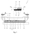
- FIG. 1 shows a power semiconductor module according to the invention in cross section.
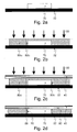
- Fig. 2 shows manufacturing steps of the method according to the invention.
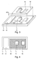
- Fig. 3 shows a three-dimensional representation of an arrangement of an insulating molded body and a substrate.
- FIG. 4 shows a plan view of the insulating molding and of the substrate according to FIG. 3.
- the power semiconductor module (1) has a housing (3) and a substrate (5) arranged therein, which consists of an insulating body (54) and of metallic laminations which are arranged on both main surfaces of the insulating body (54).
- the heat sink (2) facing metallic lamination (56) of the second main surface of the insulating body (54) is used for thermal coupling, is flat and not structured in itself.
- the lining of the first main surface of the insulating body (54) facing the power semiconductor module interior is structured in itself and thus forms the connecting tracks (52) of the substrate (5).
- the connecting elements (42, 44) of the power terminals are formed by metal moldings which are connected at their one end by way of example by soldering with the associated connecting track (52) and at its other end have a recess for screw connection.
- the power semiconductor components (70), shown here as power diodes, are arranged on the connection tracks (52).
- the circuit-compatible connection of the power diodes (70) with each other and with a connection element (40) is designed as a flexible printed circuit board (40).
- the electrically conductive connection between the power diodes (70) and the flexible printed circuit board (40) is designed as a pressure sintered connection, that between the power semiconductor component (70) and the connecting tracks (52) as a solder connection.
- the power semiconductor module has an insulation molding (80). This surrounds the power diodes (70) on all sides, wherein the contact surface (90) between the insulating molding (80) and the edge of the power semiconductor device (70) has a greater height (900) than half the thickness (700) of the power semiconductor device (70). This is crucial to prevent edge flashovers on the power semiconductor device (70). Furthermore, enough this insulating shaped body (80) to the connection element (42) of positive polarity and is electrically conductively connected to at least one surface of this connection element (42).
- the insulating molded body (80) in this case covers two printed conductors (52) and due to the described manufacturing method of the power semiconductor module (1) by means of pressure sintering technique, a portion of the insulating molded body (80) extends into the gap between the two conductor tracks (52).
- FIG. 2 shows manufacturing steps of the method according to the invention.
- a first embodiment variant of the method according to the invention is based on a substrate with a conductor track (52) arranged thereon.
- At least one power semiconductor component (70) with a suitably formed intermediate layer for pressure sintering connection is arranged on this conductor track (52) (FIG. 2 a).
- This power semiconductor component on all sides comprising an insulating molded body (80 a / b) is arranged (Fig. 2b).
- This preferably has a thickness between 2 of 100 and 10 of 100 greater than the thickness of the power semiconductor device (70).
- the distance between the edges of the power semiconductor device (70) and the comprehensive insulating molding (80) is preferably between 10/100 and 30/100 of the thickness of the power semiconductor device (70).
- This insulating shaped body (80) is preferably formed from a plastic which is deformable at least once under pressure and, if appropriate, additional temperature loading. A non-reversible deformation is particularly advantageous here.
- This deformation which is preferably associated with a preceding and / or simultaneous temperature application at a temperature between 50 ° C and 300 ° C, reduces the thickness of the insulating molded body (80) to the thickness of the power semiconductor device (70), wherein the insulating molded body (80 ) simultaneously expands laterally (86).
- the gap between the power semiconductor component (70) and insulating molded body (80) is closed, whereby this insulating molded body (80) thus surrounds the power semiconductor component (70) before the pressure is applied to the power semiconductor component (70).
- the contact surfaces (90) preferably have a height which is greater than half the thickness of the power semiconductor component (70). Due to the suitably chosen material of the insulating molding (80), this composite remains and serves in a power semiconductor module (1) of the inner insulation and prevented by its design during operation edge flashovers of the power semiconductor device (70).
- the insulation molding After completion of the pressure sintering process and in use in the power semiconductor module, the insulation molding has the same (FIG. 2 d) or a slightly greater thickness than the enclosed power semiconductor component.
- a flexible printed circuit board (40) or at least one connecting rail is arranged as a connecting element above the power semiconductor component (70) and on the insulating body (80) before the pressure sintering process (FIG. 2c).
- the areas that later form the contact surfaces between the power semiconductor device (70) and the connector (40) are prepared accordingly for a pressure sintering process.
- a suitable noble metal surface is formed on the power semiconductor component (70) and on the connecting element (40).
- a sintered metal is suitably arranged.
- a pressure sintered connection between this and the power semiconductor device (70) and at the same time between the power semiconductor device (70) and the conductor track (52) of the substrate (5) is formed.
- a third embodiment variant of the method according to the invention is based on a power semiconductor component (70) (FIG. 2 a) soldered onto the assigned conductor track (52) of a substrate (5), which is encompassed by an insulating die body (80) and wherein a flexible conductor track (40). is arranged on this.
- the sintering process thus creates a sintered connection between the power semiconductor component (70) and the connecting element (40).
- a plurality of power semiconductor components (70) can simultaneously be connected to printed conductors (52) and / or to connecting elements (40) in a single printing sintering process by arranging the insulating molded body (80).
- Fig. 3 shows a three-dimensional representation of the arrangement of the insulating molded body (80) and the substrate (5).
- the starting point for the production of the power semiconductor module (1) described with reference to FIG. 1 according to the manufacturing method described under FIG. 2 is a substrate according to the prior art.
- This has an insulating body (54), in this case an aluminum oxide ceramic, and copper conductor tracks (52) formed thereon.
- These copper conductor tracks (52) have a further layer of a noble metal, preferably gold, at least in those areas which serve as contact surfaces for a pressure sintered connection.
- the sintered metal is applied to these contact surfaces, preferably by means of a screen printing process.
- the power semiconductor components (70) are arranged.
- the power semiconductor components (70) comprising the insulating molded body (80) is then arranged. Its thickness is greater than that of the power semiconductor component (70) by 2 from 100 to 10 of 100.
- the length (802) of the recess (86) of the insulating molding (80) here is between 20 of 100 and 60 of 100 of the thickness of the power semiconductor device (70) greater than the length (702) of the power semiconductor device (70). The same applies to the width (804) of the recess (86) and the width (704) of the power semiconductor component (70).
- FIG. 4 shows a plan view of the insulating molded body (80) and the substrate (5) according to FIG. 3.
- the insulating molded body (80) shows a plan view of the insulating molded body (80) and the substrate (5) according to FIG. 3.
- the embracing of the power semiconductor component (70) by the insulating molded body (80) without these touching each other before the pressure sintering process, seen.
Abstract
Description
Die Erfindung beschreibt ein Leistungshalbleitermodul bestehend aus einem Gehäuse mit mindestens einem darin angeordneten elektrisch isolierenden Substrat vorzugsweise zur direkten Montage auf einem Kühlkörper. Das Substrat besteht aus einem Isolierstoffkörper mit einer Mehrzahl darauf befindlicher gegeneinander isolierter metallischer Verbindungsbahnen und hierauf befindlichen und mit diesen Verbindungsbahnen schaltungsgerecht verbundenen Leistungshalbleiterbauelementen. Weiterhin weist das Leistungshalbleitermodul Anschlusselemente für externe Last- und Hilfsanschlüsse und auch Verbindungselemente für Verbindungen im Inneren des Leistungshalbleitermoduls auf. Weiterhin wird ein Verfahren zur Herstellung eines oben genannten Leistungshalbleitermoduls beschrieben.The invention describes a power semiconductor module comprising a housing with at least one electrically insulating substrate arranged therein, preferably for direct mounting on a heat sink. The substrate consists of an insulating body with a plurality of mutually insulated metallic interconnect tracks located thereon and power semiconductor components located thereon and connected in a circuitally correct manner to these interconnect tracks. Furthermore, the power semiconductor module has connection elements for external load and auxiliary connections and also connection elements for connections in the interior of the power semiconductor module. Furthermore, a method for producing a power semiconductor module mentioned above is described.
Leistungshalbleitermodule, die Ausgangspunkt dieser Erfindung sind, sind beispielhaft bekannt aus der
Gemäß der als Stand der Technik genannten Druckschrift sind diese Substrate derartiger Leistungshalbieitermodule ausgebildet als elektrisch isolierende Substrate bestehend aus einem Isolierstoffkörper als Trägermaterial und zur elektrischen Isolierung zu einer Grundplatte oder zu einem Kühlkörper. Dieser Isolierstoffkörper besteht nach dem Stand der Technik aus einer Industriekeramik beispielhaft Aluminiumoxid oder Aluminiumnitrit. Auf diesem Isolierstoffkörper auf dessen dem Inneren des Leistungshalbleitermoduls zugewandten ersten Hauptfläche befinden sich eine Mehrzahl von gegeneinander elektrisch isolierten metallischen Verbindungsbahnen. Auf diesen wiederum sind die Leistungshalbleiterbauelemente angeordnet.According to the document cited as prior art, these substrates of such power semiconductor modules are designed as electrically insulating substrates consisting of an insulating body as carrier material and for electrical insulation to a base plate or to a heat sink. This Isolierstoffkörper consists of the prior art from an industrial ceramics exemplified alumina or aluminum nitrite. On this insulating body on the inside of the power semiconductor module facing the first main surface are a plurality of mutually electrically insulated metallic interconnect tracks. In turn, the power semiconductor components are arranged on these.
Meist weist der Isolierstoffkörper auf seiner dem Inneren des Leistungshalbleitermoduls abgewandten zweiten Hauptfläche ebenfalls eine metallische Schicht gleichen Materials und gleicher Dicke wie diejenige der Verbindungsbahnen auf der ersten Hauptfläche auf. In der Regel ist diese Schicht allerdings nicht in sich strukturiert, da sie beispielhaft der Lötverbindung zu einer Grundplatte oder zur thermisch leitenden Verbindung zu einem Kühlkörper dient. Die Verbindungsbahnen sowie die metallische Schicht der zweiten Hauptfläche bestehen vorzugsweise aus nach dem DCB (direct copper bonding) Verfahren aufgebrachten Kupfer, wobei das Kupfer hierbei eine typische Dicke von weniger als 1 mm aufweist.In most cases, the insulating material body also has on its second main surface facing away from the interior of the power semiconductor module a metallic layer of the same material and the same thickness as that of the connecting tracks on the first main surface. In general, however, this layer is not structured in itself, since it serves as an example of the solder joint to a base plate or the thermally conductive connection to a heat sink. The connecting tracks as well as the metallic layer of the second main surface preferably consist of copper applied by the DCB (direct copper bonding) method, the copper in this case having a typical thickness of less than 1 mm.
Häufig beschriebene Verbindungselemente zwischen den Leistungshalbleiterbauelementen und den Verbindungsbahnen sind Bondverbindungen und hier speziell Drahtbondverbindungen. Die oben genannte Druckschrift offenbart als alternative Lösung der schaltungsgerechten Verbindungen der Leistungshalbleiterbauelemente miteinander und / oder mit Verbindungsbahnen eine flexible Leiterplatte, die mit den Leistungshalbleiterbauelementen und / oder den Verbindungsbahnen mittels Lötverbindungen stoffbündig erfolgt oder mittels Druckkontakttechnik stoffschlüssig erfolgt. Die offenbarte Leiterplatte weist hierzu einen Mehrschichtaufbau auf, um sowohl Lastanschlussverbindungen, wie auch Steuer- und Hilfsanschlussverbindungen bereitzustellen. Innerhalb eines Schichtaufbaus dieser flexiblen Leiterplatte können einzelne Schichten strukturiert und / oder mit anderen Schichten oder Schichtabschnitten mittels Durchkontaktierungen verbunden sein.Frequently described connecting elements between the power semiconductor components and the connecting tracks are bonding connections and here especially wire bonds. The abovementioned document discloses as an alternative solution of the circuit-compatible connections of the power semiconductor components with each other and / or with interconnect tracks a flexible printed circuit board, which is flush with the power semiconductor devices and / or the interconnect tracks by means of solder connections or by means of pressure contact technology materially. For this purpose, the disclosed printed circuit board has a multilayer construction in order to provide both load connection connections as well as control and auxiliary connection connections. Within a layer structure of this flexible printed circuit board, individual layers can be structured and / or connected to other layers or layer sections by means of plated-through holes.
Zur Inneren Isolation sind vielfältig Leistungshalbleitermodule bekannt, die im Bereich der Leistungshalbleiterbauelemente und bis oberhalb der Verbindungselemente, die hierbei häufig als Bondverbindungen ausgestaltet sind, mit einer Vergussmasse mit hoher Dielektrizitätskonstante vergossen sind. Die oben genannte Druckschrift
Nachteilig an der Ausgestaltung eines Leistungshalbleitermoduls nach oben genannter Druckschrift ist, dass die Isolationszwischenlagen ausschließlich der inneren Isolation des Leistungshalbleitermoduls dienen und somit die Herstellung eines derartig ausgebildeten Leistungshalbleitermoduls im Vergleich zu einem mit Vergussmasse bei gleichem Nutzen aufwendiger ist, da die Isolationszwischenlagen angepasst und in einem zusätzlichen Schritt von einem Vorprodukt zu einer festen Isolationslage weiterbehandelt werden müssen. Weiterhin nachteilig ist, dass die Kanten der Isolationszwischenlage zusätzlich beschichtet werden müssen, um Spannungsüberschläge sicher zu verhindern.A disadvantage of the embodiment of a power semiconductor module according to the cited document is that the insulating liners serve exclusively the internal insulation of the power semiconductor module and thus the production of such a trained power semiconductor module is more expensive compared to a potting compound with the same benefit, since the insulation liners adapted and in an additional Step must be treated by a precursor to a solid insulation layer. Another disadvantage is that the edges of the insulation liner must also be coated to safely prevent flashovers.
Beispielhaft aus der
Der Erfindung liegt die Aufgabe zugrunde ein Leistungshalbleitermodul und ein zugehöriges Herstellungsverfahren vorzustellen wobei ein Mittel zur inneren Isolation eine Mehrzahl von Funktionen aufweist und einer rationellen Fertigung zugänglich ist.The object of the invention is to present a power semiconductor module and an associated production method, wherein a means for internal isolation has a plurality of functions and is accessible for rational production.
Die Aufgabe wird erfindungsgemäß gelöst, durch die Maßnahmen der Merkmale der Ansprüche 1 und 2. Bevorzugte Ausführungsformen sind in den Unteransprüchen beschrieben.The object is achieved by the measures of the features of
Der erfinderische Gedanke geht aus von einem Leistungshalbleitermodul vorzugsweise zur direkten Montage auf einem Kühlkörper oder mit einer Grundplatte. Dieses Leistungshalbleitermodul weist mindestens folgende Komponenten auf: ein Gehäuse, Anschlusselemente für Last- und Hilfsanschlüsse, mindestens ein Substrat mit Verbindungsbahnen und mindestens ein Leistungshalbleiterbauelement.The inventive idea is based on a power semiconductor module, preferably for direct mounting on a heat sink or with a base plate. This power semiconductor module has at least the following components: a housing, connecting elements for load and auxiliary terminals, at least one substrate with connecting tracks and at least one power semiconductor component.
Die Anschlusselemente für die Lastanschlüsse führen aus dem Gehäuse heraus und dienen der elektrischen Verbindung der im Gehäuseinneren angeordneten Leistungshalbleiterbauelemente. Das zur Grundplatte oder einem Kühlkörper elektrisch isolierend ausgebildeten Substrat besteht seinerseits aus einem Isolierstoffkörper, vorzugsweise einer Industriekeramik, und hierauf, auf dessen der Grundplatte oder dem Kühlkörper abgewandten ersten Hauptfläche befindlich, einer Mehrzahl von gegeneinander elektrisch isolierten metallischen Verbindungsbahnen. Auf diesen Verbindungsbahnen sind Leistungshalbleiterbauelemente angeordnet und schaltungsgerecht mittels Verbindungselementen verbunden. Diese Verbindungselemente sind hier beispielhaft ausgebildet als eine flexible Leiterplatte nach dem oben genannten Stand der Technik oder als bekannte Verschienung mittels in Stanz- Biegetechnik hergestellter metallsicher Verbindungsschienen.The connection elements for the load connections lead out of the housing and serve for the electrical connection of the power semiconductor components arranged inside the housing. The base plate or a heat sink electrically insulating formed substrate in turn consists of a Isolierstoffkörper, preferably an industrial ceramic, and thereon, on which the base plate or the heat sink facing away from the first main surface befindlich, a plurality of mutually electrically insulated metallic interconnect tracks. Power semiconductor components are arranged on these connecting tracks and are connected in a circuit-compatible manner by means of connecting elements. These connecting elements are here exemplified as a flexible printed circuit board according to the above-mentioned prior art or as a known busbar by means of stamped and bent metal-safe connecting rails.
Das Leistungshalbleitermodul weist weiterhin mindestens einen Isolationsformkörper auf, der mindestens ein Leistungshalbleiterbauelement umschließt und nach einem im Folgenden beschriebenen Verfahren derart verformt ausgebildet ist, dass er allseits an den Rändern des zugeordneten Leistungshalbleiterbauelements anliegt und umschließt. Das zugeordnete Verbindungselement ist hierbei beispielhaft als flexible Leiterplatte ausgestaltet und verbindet das von dem Isolationsformkörper umschlossen Leistungshalbleiterbauelement beispielhaft mit einem Anschlusselement oder einem weiteren Leistungshalbleiterbauelement. Die elektrisch leitende Verbindung des Leistungshalbleiterbauelements zur zugeordneten Leiterbahn des Substrats und / oder zum Verbindungselement, hier der flexiblen Leiterplatte, ist als Drucksinterverbindung ausgebildet.The power semiconductor module furthermore has at least one insulation molded body which surrounds at least one power semiconductor component and is deformed in a manner described below in such a way that it bears against and surrounds the edges of the associated power semiconductor component. The associated connecting element is configured in this case as a flexible printed circuit board, for example, and connects the power semiconductor component enclosed by the insulating molded body by way of example to a connecting element or a further power semiconductor component. The electrically conductive connection of the power semiconductor component to the associated conductor track of the substrate and / or to the connecting element, here the flexible printed circuit board, is designed as a pressure sintered connection.
Das erfindungsgemäße Verfahren zur Herstellung eines Leistungshalbleiterbauelements weist außer bekannten Herstellungsschritten für Leistungshalbleitermodule noch die folgenden auf:
- Anordnen mindestens eines, mindestens einmalig verformbaren, Isolationsformkörpers, wobei dieser mindestens ein Leistungshalbleiterbauelement auf dem Substrat umfasst und hierbei nicht an den Rändern des Leistungshalbleiterbauelements anliegt. Dieser Isolationsformkörper weist eine größere Höhe auf als das umfasste Leistungshalbleiterbauelement. Weiterhin ist sind der Isolationsformkörper und das Leistungshalbleiterbauelement derart zueinander angeordnet, dass zwischen dem Isolationsformkörper und dem Leistungshalbleiterbauelement dieses umfassend ein Spalt mit im Wesentlichen gleicher Breite auf allen Seiten ausgebildet ist.
- Vorzugsweise zusätzliche Anordnung mindestens eines Verbindungselements zur schaltungsgerechten Verbindung des Leistungshalbleiterbauelements oberhalb dieses Leistungshalbleiterbauelements und des dieses umfassenden Isolationsformkörpers.
- Druckbeaufschlagung im Rahmen eines Drucksinterprozesses auf das Verbindungselement oder direkt auf das mindestens eine Leistungshalbleiterbauelement und den umfassenden Isolationsformkörper. Hierbei wird eine Drucksinterverbindung des Leistungshalbleiterbauelement mit einer Leiterbahn des Substrats und / oder mit dem Verbindungselementen ausgebildet. Bei beiden Ausgestaltungen dieser Druckbeaufschlagung vorzugsweise mit zusätzlicher Temperaturbeaufschlagung verformt sich der Isolationsformkörper derart, dass er allseits an den Rändern des Leistungshalbleiterbauelements anliegt und somit das Leistungshalbleiterbauelement umschließt. Dieses Anliegen des Isolationsformkörpers verhindert eine Zerstörung des Leistungshalbleiterbauelements während des Drucksinterprozesses.
- Arranging at least one, at least once deformable, insulating molded body, which comprises at least one power semiconductor component on the substrate and in this case is not applied to the edges of the power semiconductor device. This insulating shaped body has a greater height than the included power semiconductor component. Furthermore, the insulation molded body and the power semiconductor component are arranged relative to one another in such a way that, between the insulation molding and the power semiconductor component, a gap having substantially the same width is formed on all sides.
- Preferably, additional arrangement of at least one connecting element for the circuit-compatible connection of the power semiconductor component above this power semiconductor component and of this comprehensive insulating molded body.
- Pressurization in the context of a pressure sintering process on the connecting element or directly to the at least one power semiconductor component and the comprehensive insulating molding. In this case, a pressure sintered connection of the power semiconductor component is formed with a conductor track of the substrate and / or with the connecting elements. In both embodiments of this pressurization, preferably with additional application of temperature, the insulation molding deforms in such a way that it rests on all sides against the edges of the power semiconductor component and thus encloses the power semiconductor component. This concern of the insulating molding prevents destruction of the power semiconductor device during the Drucksinterprozesses.
Die erfinderische Lösung wird an Hand der Fig. 1 bis 4 weiter erläutert.The inventive solution is further explained with reference to FIGS. 1 to 4.
Fig. 1 zeigt ein erfindungsgemäßes Leistungshalbleitermodul im Querschnitt.1 shows a power semiconductor module according to the invention in cross section.
Fig. 2 zeigt Herstellungsschritte des erfindungsgemäßen Verfahrens.Fig. 2 shows manufacturing steps of the method according to the invention.
Fig. 3 zeigt in dreidimensionaler Darstellung eine Anordnung eines Isolationsformkörpers und eines Substrats.Fig. 3 shows a three-dimensional representation of an arrangement of an insulating molded body and a substrate.
Fig. 4 zeigt eine Draufsicht des Isolationsformkörpers und des Substrats nach Fig. 3.4 shows a plan view of the insulating molding and of the substrate according to FIG. 3.
Fig. 1 zeigt ein erfindungsgemäßes Leistungshalbleitermodul (1) zur direkten Montage auf einem Kühlkörper (2). Das Leistungshalbleitermodul (1) weist ein Gehäuse (3) sowie ein hierin angeordnetes Substrat (5)auf, das aus einem Isolierstoffkörper (54) sowie aus metallischen Kaschierungen, die auf beiden Hauptflächen des Isolierstoffkörpers (54) angeordnet sind, besteht. Die dem Kühlkörper (2) zugewandte metallische Kaschierung (56) der zweiten Hauptfläche des Isolierstoffkörpers (54) dient der thermischen Ankopplung, ist flächig ausgebildet und in sich nicht strukturiert. Demgegenüber ist die dem Leistungshalbleitermodulinneren zugewandte Kaschierung der ersten Hauptfläche des Isolierstoffkörpers (54) in sich strukturiert und bildet somit die Verbindungsbahnen (52) des Substrats (5) aus.1 shows a power semiconductor module (1) according to the invention for direct mounting on a heat sink (2). The power semiconductor module (1) has a housing (3) and a substrate (5) arranged therein, which consists of an insulating body (54) and of metallic laminations which are arranged on both main surfaces of the insulating body (54). The heat sink (2) facing metallic lamination (56) of the second main surface of the insulating body (54) is used for thermal coupling, is flat and not structured in itself. On the other hand, the lining of the first main surface of the insulating body (54) facing the power semiconductor module interior is structured in itself and thus forms the connecting tracks (52) of the substrate (5).
Die Anschlusselemente (42, 44) der Leistungsanschlüsse werden gebildet durch Metallformkörper, die an ihrem einen Ende beispielhaft löttechnisch mit der zugeordneten Verbindungsbahn (52) verbunden sind und an ihrem anderen Ende eine Ausnehmung zur Schraubverbindung aufweisen.The connecting elements (42, 44) of the power terminals are formed by metal moldings which are connected at their one end by way of example by soldering with the associated connecting track (52) and at its other end have a recess for screw connection.
Auf den Verbindungsbahnen (52) sind die Leistungshalbleiterbauelemente (70), hier dargestellt Leistungsdioden, angeordnet. Die schaltungsgerechte Verbindung der Leistungsdioden (70) miteinander und mit einem Anschlusselement (40) ist als flexible Leiterplatte (40) ausgebildet. Die elektrisch leitende Verbindung zwischen den Leistungsdioden (70) und der flexiblen Leiterplatte (40) ist als Drucksinterverbindung, diejenige zwischen den Leistungshalbleiterbauelement (70) und den Verbindungsbahnen (52) als Lötverbindung ausgebildet.The power semiconductor components (70), shown here as power diodes, are arranged on the connection tracks (52). The circuit-compatible connection of the power diodes (70) with each other and with a connection element (40) is designed as a flexible printed circuit board (40). The electrically conductive connection between the power diodes (70) and the flexible printed circuit board (40) is designed as a pressure sintered connection, that between the power semiconductor component (70) and the connecting tracks (52) as a solder connection.
Zur inneren elektrischen Isolation weist das Leistungshalbleitermodul einen Isolationsformkörper (80) auf. Dieser umschließt die Leistungsdioden (70) allseits, wobei die Kontaktfläche (90) zwischen dem Isolationsformkörper (80) und dem Rand des Leistungshalbleiterbauelements (70) eine größere Höhe (900) aufweist als die halbe Dicke (700) des Leistungshalbleiterbauelements (70). Dies ist entscheidend um Randüberschläge am Leistungshalbleiterbauelement (70) zu verhindern. Weiterhin reicht dieser Isolationsformkörper (80) bis zum Anschlusselement (42) positiver Polarität und ist mit mindestens einer Fläche dieses Anschlusselements (42) elektrisch leitend verbunden. Da der Isolationsformkörper (80) hierbei zwei Leiterbahnen (52) überdeckt und aufgrund des beschriebenen Herstellungsverfahren des Leistungshalbleitermoduls (1) mittels Drucksintertechnik reicht ein Teil des Isolationsformkörpers (80) in den Spalt zwischen den beiden Leiterbahnen (52) hinein.For internal electrical insulation, the power semiconductor module has an insulation molding (80). This surrounds the power diodes (70) on all sides, wherein the contact surface (90) between the insulating molding (80) and the edge of the power semiconductor device (70) has a greater height (900) than half the thickness (700) of the power semiconductor device (70). This is crucial to prevent edge flashovers on the power semiconductor device (70). Furthermore, enough this insulating shaped body (80) to the connection element (42) of positive polarity and is electrically conductively connected to at least one surface of this connection element (42). Since the insulating molded body (80) in this case covers two printed conductors (52) and due to the described manufacturing method of the power semiconductor module (1) by means of pressure sintering technique, a portion of the insulating molded body (80) extends into the gap between the two conductor tracks (52).
Fig. 2 zeigt Herstellungsschritte des erfindungsgemäßen Verfahrens. Eine erste Ausführungsvariante des erfindungsgemäßen Verfahrens geht aus von einem Substrat mit einer darauf angeordneten Leiterbahn (52). Auf dieser Leiterbahn (52) wird mindestens ein Leistungshalbleiterbauelement (70) mit einer geeignet ausgebildeten Zwischenschicht zur Drucksinterverbindung anordnet (Fig. 2a). Diese Leistungshalbleiterbauelement allseits umfassend wird ein lsolationsformkörper (80 a/b) angeordnet (Fig. 2b). Dieser weist vorzugsweise ein Dicke auf, die zwischen 2 von 100 und 10 von 100 größer ist als die Dicke des Leistungshalbleiterbauelements (70). Der Abstand zwischen den Ränder des Leistungshalbleiterbauelement (70) und dem umfassenden Isolationsformkörper (80) beträgt vorzugsweise zwischen 10 von 100 und 30 von 100 der Dicke des Leistungshalbleiterbauelements (70). Dieser Isolationsformkörper (80) ist vorzugsweise aus einem mindestens einmalig unter Druck und gegebenenfalls zusätzlicher Temperaturbeaufschlagung verformbaren Kunststoff ausgebildet. Eine nicht reversible Verformung ist hierbei besonders vorteilhaft.Fig. 2 shows manufacturing steps of the method according to the invention. A first embodiment variant of the method according to the invention is based on a substrate with a conductor track (52) arranged thereon. At least one power semiconductor component (70) with a suitably formed intermediate layer for pressure sintering connection is arranged on this conductor track (52) (FIG. 2 a). This power semiconductor component on all sides comprising an insulating molded body (80 a / b) is arranged (Fig. 2b). This preferably has a thickness between 2 of 100 and 10 of 100 greater than the thickness of the power semiconductor device (70). The distance between the edges of the power semiconductor device (70) and the comprehensive insulating molding (80) is preferably between 10/100 and 30/100 of the thickness of the power semiconductor device (70). This insulating shaped body (80) is preferably formed from a plastic which is deformable at least once under pressure and, if appropriate, additional temperature loading. A non-reversible deformation is particularly advantageous here.
Im Anschluss erfolgt die plane Druckbeaufschlagung (100) auf das Leistungshalbleiterbauelement (70) und den Isolierstoffkörper (80), der sich hierbei verformt. Diese Verformung, die vorzugsweise mit einer vorangehenden und / oder gleichzeitigen Temperaturbeaufschlagung mit einer Temperatur zwischen 50°C und 300°C verbunden ist, verringert die Dicke des Isolationsformkörpers (80) auf die Dicke des Leistungshalbleiterbauelements (70), wobei sich der Isolationsformkörper (80) gleichzeitig seitlich ausdehnt (86). Hierdurch wird der Spalt zwischen dem Leistungshalbleiterbauelement (70) und Isolationsformkörper (80) geschlossen wodurch dieser Isolationsformkörper (80) somit das Leistungshalbleiterbauelement (70) umschließt bevor die Druckeinleitung auf das Leistungshalbleiterbauelement (70) erfolgt. Die Kontaktflächen (90) weisen hierbei vorzugsweise eine Höhe auf, die größer ist als die halbe Dicke des Leistungshalbleiterbauelements (70). Durch den geeignet gewählten Werkstoff des Isolationsformkörpers (80) verbleibt dieser Verbund bestehen und dient in einem Leistungshalbleitermodul (1) der inneren Isolation und verhindert durch seine Ausgestaltung im Betrieb Randüberschläge des Leistungshalbleiterbauelements (70).This is followed by the planar pressurization (100) to the power semiconductor component (70) and the insulating body (80), which deforms in this case. This deformation, which is preferably associated with a preceding and / or simultaneous temperature application at a temperature between 50 ° C and 300 ° C, reduces the thickness of the insulating molded body (80) to the thickness of the power semiconductor device (70), wherein the insulating molded body (80 ) simultaneously expands laterally (86). As a result, the gap between the power semiconductor component (70) and insulating molded body (80) is closed, whereby this insulating molded body (80) thus surrounds the power semiconductor component (70) before the pressure is applied to the power semiconductor component (70). In this case, the contact surfaces (90) preferably have a height which is greater than half the thickness of the power semiconductor component (70). Due to the suitably chosen material of the insulating molding (80), this composite remains and serves in a power semiconductor module (1) of the inner insulation and prevented by its design during operation edge flashovers of the power semiconductor device (70).
Nach Beendigung des Drucksinterprozesses und im Einsatz im Leistungshalbleitermodul weist der Isolationsformkörper die gleiche (Fig. 2d) oder eine geringfügig größere Dicke als das umschlossene Leistungshalbleiterbauelement auf.After completion of the pressure sintering process and in use in the power semiconductor module, the insulation molding has the same (FIG. 2 d) or a slightly greater thickness than the enclosed power semiconductor component.
In einer zweiten Ausführungsvariante des erfindungsgemäßen Verfahrens wird vor dem Drucksinterprozess noch eine flexible Leiterplatte (40) oder mindestens eine Verbindungsschiene als Verbindungselement oberhalb des Leistungshalbleiterbauelements (70) und auf dem Isolierstoffkörper (80) angeordnet (Fig. 2c). Die Bereiche, die später die Kontaktflächen zwischen dem Leistungshalbleiterbauelement (70) und dem Verbindungselement (40) ausbilden sind für ein Drucksinterverfahren entsprechend vorbereitet. Es ist hierzu im Bereich der Kontaktflächen eine geeignet Edelmetalloberfläche auf dem Leistungshalbleiterbauelement (70) und auf dem Verbindungselement (40) ausgebildet. Ebenso ist ein Sintermetall geeignet angeordnet. Bei einer plan eingeleiteten Druck- und vorzugsweise gleichzeitiger Temperaturbeaufschlagung auf das Verbindungselement (40) wird eine Drucksinterverbindung zwischen dieser und dem Leistungshalbleiterbauelement (70) und gleichzeitig zwischen dem Leistungshalbleiterbauelement (70) und der Leiterbahn (52) des Substrats (5) ausgebildet.In a second embodiment of the method according to the invention, a flexible printed circuit board (40) or at least one connecting rail is arranged as a connecting element above the power semiconductor component (70) and on the insulating body (80) before the pressure sintering process (FIG. 2c). The areas that later form the contact surfaces between the power semiconductor device (70) and the connector (40) are prepared accordingly for a pressure sintering process. For this purpose, in the area of the contact surfaces, a suitable noble metal surface is formed on the power semiconductor component (70) and on the connecting element (40). Likewise, a sintered metal is suitably arranged. In a plan initiated pressure and preferably simultaneous temperature application to the connecting element (40) a pressure sintered connection between this and the power semiconductor device (70) and at the same time between the power semiconductor device (70) and the conductor track (52) of the substrate (5) is formed.
Eine dritte Ausführungsvariante des erfindungsgemäßen Verfahrens geht aus von einem auf die zugeordnete Leiterbahn (52) eines Substrats (5) gelöteten Leistungshalbleiterbauelement (70) (Fig. 2a), welches von einem Isolationsformköper (80) umfasst wird und wobei eine flexible Leiterbahn (40) auf diesem angeordnet ist. Durch den Drucksinterprozess wird somit eine Sinterverbindung zwischen dem Leistungshalbleiterbauelement (70) und der Verbindungselement (40) geschaffen.A third embodiment variant of the method according to the invention is based on a power semiconductor component (70) (FIG. 2 a) soldered onto the assigned conductor track (52) of a substrate (5), which is encompassed by an insulating die body (80) and wherein a flexible conductor track (40). is arranged on this. The sintering process thus creates a sintered connection between the power semiconductor component (70) and the connecting element (40).
Vorteilhaft an allen oben beschriebenen Ausführungsformen des Verfahrens ist, dass in einem einzigen Drucksinterprozess, durch die Anordnung des Isolationsformkörpers (80), gleichzeitig eine Mehrzahl von Leistungshalbleiterbauelementen (70) mit Leiterbahnen (52) und / oder mit Verbindungselementen (40) verbunden werden können.It is advantageous in all embodiments of the method described above that a plurality of power semiconductor components (70) can simultaneously be connected to printed conductors (52) and / or to connecting elements (40) in a single printing sintering process by arranging the insulating molded body (80).
Fig. 3 zeigt in dreidimensionaler Darstellung die Anordnung des Isolationsformkörpers (80) und des Substrats (5). Ausgangspunkt der Herstellung des unter Fig. 1 beschriebenen Leistungshalbleitermoduls (1) gemäß dem unter Fig. 2 beschriebenen Herstellungsverfahrens ist ein Substrat nach dem Stand der Technik. Dieses weist einen Isolierstoffkörper (54), hier einer Aluminiumoxidkeramik, und hierauf ausgebildeten Kupferleiterbahnen (52) auf. Diese Kupferleiterbahnen (52) weisen zumindest in denjenigen Bereichen, die als Kontaktflächen für eine Drucksinterverbindung dienen eine weitere Schicht eines Edelmetalls, vorzugsweise Gold, auf. Auf diese Kontaktflächen wird das Sintermetall, vorzugsweise mittels eines Siebdruckverfahrens, aufgebracht. Anschließend werden die Leistungshalbleiterbauelemente (70) angeordnet. Die Leistungshalbleiterbauelemente (70) umfassend wird dann der Isolationsformkörper (80) angeordnet. Dessen Dicke ist hierbei um 2 von 100 bis 10 von 100 größer als diejenige des Leistungshalbleiterbauelements (70). Die Länge (802) der Aussparung (86) des Isolationsformkörpers (80) ist hierbei zwischen 20 von 100 und 60 von 100 der Dicke des Leistungshalbleiterbauelements (70) größer als die Länge (702) des Leistungshalbleiterbauelements (70). Gleiches gilt für die Breite (804) der Aussparung (86) und die Breite (704) des Leistungshalbleiterbauelements (70).Fig. 3 shows a three-dimensional representation of the arrangement of the insulating molded body (80) and the substrate (5). The starting point for the production of the power semiconductor module (1) described with reference to FIG. 1 according to the manufacturing method described under FIG. 2 is a substrate according to the prior art. This has an insulating body (54), in this case an aluminum oxide ceramic, and copper conductor tracks (52) formed thereon. These copper conductor tracks (52) have a further layer of a noble metal, preferably gold, at least in those areas which serve as contact surfaces for a pressure sintered connection. The sintered metal is applied to these contact surfaces, preferably by means of a screen printing process. Subsequently, the power semiconductor components (70) are arranged. The power semiconductor components (70) comprising the insulating molded body (80) is then arranged. Its thickness is greater than that of the power semiconductor component (70) by 2 from 100 to 10 of 100. The length (802) of the recess (86) of the insulating molding (80) here is between 20 of 100 and 60 of 100 of the thickness of the power semiconductor device (70) greater than the length (702) of the power semiconductor device (70). The same applies to the width (804) of the recess (86) and the width (704) of the power semiconductor component (70).
Fig. 4 zeigt eine Draufsicht auf den Isolationsformkörper (80) und das Substrats (5) gemäß Fig. 3. Hierbei ist nochmals deutlich das Umfassen des Leistungshalbleiterbauelements (70) durch den Isolationsformköper (80), ohne dass diese sich vor dem Drucksinterprozess berühren, ersichtlich.FIG. 4 shows a plan view of the insulating molded body (80) and the substrate (5) according to FIG. 3. Here again clearly the embracing of the power semiconductor component (70) by the insulating molded body (80), without these touching each other before the pressure sintering process, seen.
Claims (7)
wobei mindestens eine Verbindung zwischen einem Leistungshalbleiterbauelement (70) und einem Verbindungselement (40) oder zwischen dem Leistungshalbleiterbauelement (70) und der Verbindungsbahn (52) als Drucksinterverbindung ausgebildet ist und
wobei der Isolationsformkörper (80) derart angeordnet ist, dass er allseits an den Rändern mindestens eines zugeordneten Leistungshalbleiterbauelements (70) anliegt und diese somit umschließt.Power semiconductor module (1) with a housing (3), outwardly leading connection elements (42, 44), at least one within the housing (3) arranged electrically insulating substrate (5), which at least consists of an insulating body (54) and on the The first main area facing the interior of the power semiconductor module is provided with a plurality of mutually electrically insulated metallic interconnect tracks and with at least one power semiconductor component (70) arranged on one of these interconnect tracks with at least one interconnect element (40) and at least one structured insulating molded body (80) )
wherein at least one connection between a power semiconductor component (70) and a connecting element (40) or between the power semiconductor component (70) and the connecting track (52) is designed as a pressure sintered connection and
wherein the insulation molding (80) is arranged such that it rests on all sides at the edges of at least one associated power semiconductor component (70) and thus encloses them.
wobei die Kontaktfläche (90) zwischen dem Isolationsformkörper (80) und dem Rand des Leistungshalbleiterbauelements (70) eine größere Höhe aufweist als die halbe Dicke (700) des Leistungshalbleiterbauelements (70).Power semiconductor module (1) according to claim 1,
wherein the contact surface (90) between the insulation molding (80) and the edge of the power semiconductor device (70) has a greater height than half the thickness (700) of the power semiconductor device (70).
wobei das Verbindungselement (40) als eine flexible Leiterplatte oder Verbindungsschiene jeweils mit flächigen Kontaktstellen zum Leistungshalbleiterbauelement (70) ausgestaltet ist.Power semiconductor module (1) according to claim 1,
wherein the connecting element (40) is designed as a flexible printed circuit board or connecting rail, each with flat contact points to the power semiconductor component (70).
wobei nach der Anordnung des Leistungshalbleiterbauelements (70) und des umfassenden Isolationsformkörpers (80) auf dem Substrat (5) mindestens
wherein after the arrangement of the power semiconductor device (70) and the comprehensive insulating shaped body (80) on the substrate (5) at least
wobei zusätzlich zur Druckbeaufschlagung (100) während und / oder vor dem Drucksinterprozess der Isolationsformkörper noch mit einer Temperatur zwischen 50°C und 300°C beaufschlagt wird.Method for producing a power semiconductor module (1) according to Claim 2 or 5, characterized
wherein, in addition to the pressurization (100) during and / or before the pressure sintering process, the insulating molding is still subjected to a temperature between 50 ° C and 300 ° C.
wobei eine Mehrzahl von Leistungshalbleiterbauelementen (70) gleichzeitig mittels eines Drucksinterprozesses mit zugeordneten Leiterbahnen (52) und / oder einem oder mehreren Verbindungselementen (40) verbunden werden.Method for producing a power semiconductor module (1) according to Claim 2,
wherein a plurality of power semiconductor devices (70) are simultaneously connected to associated conductive traces (52) and / or one or more interconnect elements (40) by a pressure sintering process.
Applications Claiming Priority (1)
| Application Number | Priority Date | Filing Date | Title |
|---|---|---|---|
| DE102005047567A DE102005047567B3 (en) | 2005-10-05 | 2005-10-05 | Power semiconductor module comprises a housing, connecting elements and an electrically insulated substrate arranged within the housing and semiconductor components with a connecting element and an insulating molded body |
Publications (2)
| Publication Number | Publication Date |
|---|---|
| EP1772902A1 true EP1772902A1 (en) | 2007-04-11 |
| EP1772902B1 EP1772902B1 (en) | 2008-09-17 |
Family
ID=37625994
Family Applications (1)
| Application Number | Title | Priority Date | Filing Date |
|---|---|---|---|
| EP06020798A Not-in-force EP1772902B1 (en) | 2005-10-05 | 2006-10-04 | Power semiconductor modul with intermediate isolating layer und method of manufacturing |
Country Status (6)
| Country | Link |
|---|---|
| EP (1) | EP1772902B1 (en) |
| JP (1) | JP5291872B2 (en) |
| AT (1) | ATE408898T1 (en) |
| DE (2) | DE102005047567B3 (en) |
| DK (1) | DK1772902T3 (en) |
| ES (1) | ES2314804T3 (en) |
Cited By (5)
| Publication number | Priority date | Publication date | Assignee | Title |
|---|---|---|---|---|
| DE102007006706A1 (en) * | 2007-02-10 | 2008-08-21 | Semikron Elektronik Gmbh & Co. Kg | Circuit arrangement with connecting device and manufacturing method thereof |
| KR20100132469A (en) * | 2009-06-09 | 2010-12-17 | 세미크론 엘렉트로니크 지엠비에치 앤드 코. 케이지 | Method for producing a converter arrangement comprising a cooling device, and converter arrangement |
| EP2146372A3 (en) * | 2008-07-16 | 2013-11-06 | Semikron Elektronik GmbH & Co. KG Patentabteilung | Power electronic connection device and production method for same |
| DE102012222012A1 (en) | 2012-11-30 | 2014-06-18 | Semikron Elektronik Gmbh & Co. Kg | Power semiconductor device e.g. insulated gate bipolar transistor (IGBT) for use in power semiconductor module, has power semiconductor component whose lateral edges are arranged on conductor line, adjacent to non-conductive insulator |
| DE102013108185A1 (en) * | 2013-07-31 | 2015-02-05 | Semikron Elektronik Gmbh & Co. Kg | Method for producing a power electronic switching device and power electronic switching device |
Families Citing this family (10)
| Publication number | Priority date | Publication date | Assignee | Title |
|---|---|---|---|---|
| DE102007022336A1 (en) | 2007-05-12 | 2008-11-20 | Semikron Elektronik Gmbh & Co. Kg | Power semiconductor substrate with metal contact layer and manufacturing method thereof |
| DE102007057346B3 (en) * | 2007-11-28 | 2009-06-10 | Fachhochschule Kiel | Laminated power electronics module |
| DE102008017454B4 (en) * | 2008-04-05 | 2010-02-04 | Semikron Elektronik Gmbh & Co. Kg | Power semiconductor module with hermetically sealed circuit arrangement and manufacturing method for this purpose |
| DE102008040488A1 (en) * | 2008-07-17 | 2010-01-21 | Robert Bosch Gmbh | Electronic assembly and method of making the same |
| DE102009024385B4 (en) * | 2009-06-09 | 2011-03-17 | Semikron Elektronik Gmbh & Co. Kg | Method for producing a power semiconductor module and power semiconductor module with a connection device |
| JP5842489B2 (en) * | 2011-09-14 | 2016-01-13 | 三菱電機株式会社 | Semiconductor device |
| DE102011083911A1 (en) * | 2011-09-30 | 2013-04-04 | Robert Bosch Gmbh | Electronic assembly with high-temperature-stable substrate base material |
| DE102014109779A1 (en) * | 2014-06-13 | 2015-12-17 | Osram Opto Semiconductors Gmbh | Method for producing an assembly with a component |
| DE102015109856A1 (en) * | 2015-06-19 | 2016-12-22 | Danfoss Silicon Power Gmbh | Method for producing a suitable for the connection of an electrical conductor metallic contact surface for contacting a power semiconductor, power semiconductor, bond buffer and method for producing a power semiconductor |
| DE102019126623B4 (en) | 2019-10-02 | 2024-03-14 | Semikron Elektronik Gmbh & Co. Kg Patentabteilung | Power electronic switching device with a casting compound |
Citations (3)
| Publication number | Priority date | Publication date | Assignee | Title |
|---|---|---|---|---|
| DE19617055C1 (en) * | 1996-04-29 | 1997-06-26 | Semikron Elektronik Gmbh | High-density multilayer prepreg semiconductor power module |
| WO2005027222A2 (en) * | 2003-09-12 | 2005-03-24 | Siemens Aktiengesellschaft | Assembly of an electrical component comprising an electrical insulation film on a substrate and method for producing said assembly |
| EP1538667A2 (en) * | 2003-12-06 | 2005-06-08 | LuK Lamellen und Kupplungsbau Beteiligungs KG | Electronic apparatus with electrically isolated metallic heat transfer body |
Family Cites Families (5)
| Publication number | Priority date | Publication date | Assignee | Title |
|---|---|---|---|---|
| DE3414065A1 (en) * | 1984-04-13 | 1985-12-12 | Siemens AG, 1000 Berlin und 8000 München | Configuration comprising at least one electronic component fixed on a substrate, and process for fabricating a configuration of this type |
| US4657322A (en) * | 1985-10-01 | 1987-04-14 | Tektronix, Inc. | Microwave interconnect |
| JPH08107266A (en) * | 1994-10-04 | 1996-04-23 | Cmk Corp | Printed-wiring board |
| DE10121970B4 (en) * | 2001-05-05 | 2004-05-27 | Semikron Elektronik Gmbh | Power semiconductor module in pressure contact |
| DE102004019567B3 (en) * | 2004-04-22 | 2006-01-12 | Semikron Elektronik Gmbh & Co. Kg | Securing electronic components to substrate by subjecting the electronic component, supporting film and paste-like layer to pressure and connecting the substrate and the component by sintering |
-
2005
- 2005-10-05 DE DE102005047567A patent/DE102005047567B3/en not_active Expired - Fee Related
-
2006
- 2006-10-04 EP EP06020798A patent/EP1772902B1/en not_active Not-in-force
- 2006-10-04 DE DE502006001588T patent/DE502006001588D1/en active Active
- 2006-10-04 JP JP2006272882A patent/JP5291872B2/en not_active Expired - Fee Related
- 2006-10-04 AT AT06020798T patent/ATE408898T1/en active
- 2006-10-04 ES ES06020798T patent/ES2314804T3/en active Active
- 2006-10-04 DK DK06020798T patent/DK1772902T3/en active
Patent Citations (3)
| Publication number | Priority date | Publication date | Assignee | Title |
|---|---|---|---|---|
| DE19617055C1 (en) * | 1996-04-29 | 1997-06-26 | Semikron Elektronik Gmbh | High-density multilayer prepreg semiconductor power module |
| WO2005027222A2 (en) * | 2003-09-12 | 2005-03-24 | Siemens Aktiengesellschaft | Assembly of an electrical component comprising an electrical insulation film on a substrate and method for producing said assembly |
| EP1538667A2 (en) * | 2003-12-06 | 2005-06-08 | LuK Lamellen und Kupplungsbau Beteiligungs KG | Electronic apparatus with electrically isolated metallic heat transfer body |
Cited By (9)
| Publication number | Priority date | Publication date | Assignee | Title |
|---|---|---|---|---|
| DE102007006706A1 (en) * | 2007-02-10 | 2008-08-21 | Semikron Elektronik Gmbh & Co. Kg | Circuit arrangement with connecting device and manufacturing method thereof |
| DE102007006706B4 (en) * | 2007-02-10 | 2011-05-26 | Semikron Elektronik Gmbh & Co. Kg | Circuit arrangement with connecting device and manufacturing method thereof |
| EP2146372A3 (en) * | 2008-07-16 | 2013-11-06 | Semikron Elektronik GmbH & Co. KG Patentabteilung | Power electronic connection device and production method for same |
| KR20100132469A (en) * | 2009-06-09 | 2010-12-17 | 세미크론 엘렉트로니크 지엠비에치 앤드 코. 케이지 | Method for producing a converter arrangement comprising a cooling device, and converter arrangement |
| EP2271196A1 (en) * | 2009-06-09 | 2011-01-05 | SEMIKRON Elektronik GmbH & Co. KG | Method for producing a frequency converter with cooling device and frequency converter |
| DE102012222012A1 (en) | 2012-11-30 | 2014-06-18 | Semikron Elektronik Gmbh & Co. Kg | Power semiconductor device e.g. insulated gate bipolar transistor (IGBT) for use in power semiconductor module, has power semiconductor component whose lateral edges are arranged on conductor line, adjacent to non-conductive insulator |
| DE102012222012B4 (en) * | 2012-11-30 | 2017-04-06 | Semikron Elektronik Gmbh & Co. Kg | Power semiconductor device and a method for producing a power semiconductor device |
| DE102013108185A1 (en) * | 2013-07-31 | 2015-02-05 | Semikron Elektronik Gmbh & Co. Kg | Method for producing a power electronic switching device and power electronic switching device |
| DE102013108185B4 (en) | 2013-07-31 | 2021-09-23 | Semikron Elektronik Gmbh & Co. Kg | Method for producing a power electronic switching device and power electronic switching device |
Also Published As
| Publication number | Publication date |
|---|---|
| ATE408898T1 (en) | 2008-10-15 |
| DE102005047567B3 (en) | 2007-03-29 |
| DE502006001588D1 (en) | 2008-10-30 |
| JP5291872B2 (en) | 2013-09-18 |
| EP1772902B1 (en) | 2008-09-17 |
| ES2314804T3 (en) | 2009-03-16 |
| DK1772902T3 (en) | 2009-01-19 |
| JP2007103948A (en) | 2007-04-19 |
Similar Documents
| Publication | Publication Date | Title |
|---|---|---|
| EP1772902B1 (en) | Power semiconductor modul with intermediate isolating layer und method of manufacturing | |
| EP1956647B1 (en) | Circuit arrangement with connecting device and corresponding production method | |
| DE102008017454B4 (en) | Power semiconductor module with hermetically sealed circuit arrangement and manufacturing method for this purpose | |
| DE102005016650B4 (en) | Power semiconductor module with butt soldered connection and connection elements | |
| DE102009042600A1 (en) | Power semiconductor module and manufacturing method for this | |
| EP1855319A2 (en) | Power semiconductor device | |
| DE102014116662B4 (en) | ELECTRICAL CONNECTION ASSEMBLY, SEMICONDUCTOR MODULE AND METHOD FOR PRODUCING A SEMICONDUCTOR MODULE | |
| WO2013013964A1 (en) | Carrier device, electrical device having a carrier device and method for producing same | |
| DE102014114808A1 (en) | Electronic module and method for producing an electronic module | |
| DE102004057421B4 (en) | Pressure-contacted power semiconductor module for high ambient temperatures and method for its production | |
| DE102005030247B4 (en) | Power semiconductor module with high current carrying capacity connectors | |
| DE102005050534B4 (en) | The power semiconductor module | |
| EP1791178A2 (en) | Pressure contact type power semiconductor module | |
| DE102011078806B4 (en) | Manufacturing method for a power electronic system with a cooling device | |
| DE202016101292U1 (en) | Power semiconductor device | |
| DE102016101726B4 (en) | Power semiconductor device and method for producing a power semiconductor device | |
| EP2964004A2 (en) | Electronic component assembly | |
| DE10121969C1 (en) | Circuit arrangement in pressure contact and method for its production | |
| DE102009050178B3 (en) | Power semiconductor module having a three-dimensional surface contour having substrate and manufacturing method thereof | |
| DE102018207360B4 (en) | BUSBAR, PROCESS FOR ITS MANUFACTURE, AND POWER MODULE COMPOSING THE SAME | |
| DE102021116053A1 (en) | Electrical conductor, electronic assembly with an electrical conductor and method for manufacturing an electronic assembly with an electrical conductor | |
| EP4189738A1 (en) | Electronic circuit module | |
| EP4211996A1 (en) | Method and cast part production system for producing an electric motor housing, and electric motor | |
| DE102006029711B4 (en) | support device | |
| EP3154081A2 (en) | Process of manufacturing electronic modules with connection of a metallic component to a ceramic surface of a substrate using a metal powder-based paste |
Legal Events
| Date | Code | Title | Description |
|---|---|---|---|
| PUAI | Public reference made under article 153(3) epc to a published international application that has entered the european phase |
Free format text: ORIGINAL CODE: 0009012 |
|
| 17P | Request for examination filed |
Effective date: 20070205 |
|
| AK | Designated contracting states |
Kind code of ref document: A1 Designated state(s): AT BE BG CH CY CZ DE DK EE ES FI FR GB GR HU IE IS IT LI LT LU LV MC NL PL PT RO SE SI SK TR |
|
| AX | Request for extension of the european patent |
Extension state: AL BA HR MK YU |
|
| 17Q | First examination report despatched |
Effective date: 20070601 |
|
| AKX | Designation fees paid |
Designated state(s): AT BE BG CH CY CZ DE DK EE ES FI FR GB GR HU IE IS IT LI LT LU LV MC NL PL PT RO SE SI SK TR |
|
| GRAP | Despatch of communication of intention to grant a patent |
Free format text: ORIGINAL CODE: EPIDOSNIGR1 |
|
| GRAS | Grant fee paid |
Free format text: ORIGINAL CODE: EPIDOSNIGR3 |
|
| GRAA | (expected) grant |
Free format text: ORIGINAL CODE: 0009210 |
|
| AK | Designated contracting states |
Kind code of ref document: B1 Designated state(s): AT BE BG CH CY CZ DE DK EE ES FI FR GB GR HU IE IS IT LI LT LU LV MC NL PL PT RO SE SI SK TR |
|
| REG | Reference to a national code |
Ref country code: GB Ref legal event code: FG4D Free format text: NOT ENGLISH |
|
| REG | Reference to a national code |
Ref country code: CH Ref legal event code: EP |
|
| REG | Reference to a national code |
Ref country code: IE Ref legal event code: FG4D Free format text: LANGUAGE OF EP DOCUMENT: GERMAN |
|
| REF | Corresponds to: |
Ref document number: 502006001588 Country of ref document: DE Date of ref document: 20081030 Kind code of ref document: P |
|
| REG | Reference to a national code |
Ref country code: CH Ref legal event code: NV Representative=s name: BRAUNPAT BRAUN EDER AG |
|
| REG | Reference to a national code |
Ref country code: SE Ref legal event code: TRGR |
|
| REG | Reference to a national code |
Ref country code: DK Ref legal event code: T3 |
|
| PG25 | Lapsed in a contracting state [announced via postgrant information from national office to epo] |
Ref country code: LT Free format text: LAPSE BECAUSE OF FAILURE TO SUBMIT A TRANSLATION OF THE DESCRIPTION OR TO PAY THE FEE WITHIN THE PRESCRIBED TIME-LIMIT Effective date: 20080917 |
|
| PG25 | Lapsed in a contracting state [announced via postgrant information from national office to epo] |
Ref country code: LV Free format text: LAPSE BECAUSE OF FAILURE TO SUBMIT A TRANSLATION OF THE DESCRIPTION OR TO PAY THE FEE WITHIN THE PRESCRIBED TIME-LIMIT Effective date: 20080917 Ref country code: SI Free format text: LAPSE BECAUSE OF FAILURE TO SUBMIT A TRANSLATION OF THE DESCRIPTION OR TO PAY THE FEE WITHIN THE PRESCRIBED TIME-LIMIT Effective date: 20080917 |
|
| REG | Reference to a national code |
Ref country code: ES Ref legal event code: FG2A Ref document number: 2314804 Country of ref document: ES Kind code of ref document: T3 |
|
| REG | Reference to a national code |
Ref country code: IE Ref legal event code: FD4D |
|
| PG25 | Lapsed in a contracting state [announced via postgrant information from national office to epo] |
Ref country code: BG Free format text: LAPSE BECAUSE OF FAILURE TO SUBMIT A TRANSLATION OF THE DESCRIPTION OR TO PAY THE FEE WITHIN THE PRESCRIBED TIME-LIMIT Effective date: 20081217 |
|
| PG25 | Lapsed in a contracting state [announced via postgrant information from national office to epo] |
Ref country code: RO Free format text: LAPSE BECAUSE OF FAILURE TO SUBMIT A TRANSLATION OF THE DESCRIPTION OR TO PAY THE FEE WITHIN THE PRESCRIBED TIME-LIMIT Effective date: 20080917 Ref country code: PT Free format text: LAPSE BECAUSE OF FAILURE TO SUBMIT A TRANSLATION OF THE DESCRIPTION OR TO PAY THE FEE WITHIN THE PRESCRIBED TIME-LIMIT Effective date: 20090217 Ref country code: MC Free format text: LAPSE BECAUSE OF NON-PAYMENT OF DUE FEES Effective date: 20081031 Ref country code: IS Free format text: LAPSE BECAUSE OF FAILURE TO SUBMIT A TRANSLATION OF THE DESCRIPTION OR TO PAY THE FEE WITHIN THE PRESCRIBED TIME-LIMIT Effective date: 20090117 Ref country code: CZ Free format text: LAPSE BECAUSE OF FAILURE TO SUBMIT A TRANSLATION OF THE DESCRIPTION OR TO PAY THE FEE WITHIN THE PRESCRIBED TIME-LIMIT Effective date: 20080917 |
|
| PLBE | No opposition filed within time limit |
Free format text: ORIGINAL CODE: 0009261 |
|
| STAA | Information on the status of an ep patent application or granted ep patent |
Free format text: STATUS: NO OPPOSITION FILED WITHIN TIME LIMIT |
|
| PG25 | Lapsed in a contracting state [announced via postgrant information from national office to epo] |
Ref country code: IE Free format text: LAPSE BECAUSE OF FAILURE TO SUBMIT A TRANSLATION OF THE DESCRIPTION OR TO PAY THE FEE WITHIN THE PRESCRIBED TIME-LIMIT Effective date: 20080917 Ref country code: EE Free format text: LAPSE BECAUSE OF FAILURE TO SUBMIT A TRANSLATION OF THE DESCRIPTION OR TO PAY THE FEE WITHIN THE PRESCRIBED TIME-LIMIT Effective date: 20080917 |
|
| 26N | No opposition filed |
Effective date: 20090618 |
|
| PG25 | Lapsed in a contracting state [announced via postgrant information from national office to epo] |
Ref country code: PL Free format text: LAPSE BECAUSE OF FAILURE TO SUBMIT A TRANSLATION OF THE DESCRIPTION OR TO PAY THE FEE WITHIN THE PRESCRIBED TIME-LIMIT Effective date: 20080917 |
|
| PG25 | Lapsed in a contracting state [announced via postgrant information from national office to epo] |
Ref country code: CY Free format text: LAPSE BECAUSE OF FAILURE TO SUBMIT A TRANSLATION OF THE DESCRIPTION OR TO PAY THE FEE WITHIN THE PRESCRIBED TIME-LIMIT Effective date: 20080917 Ref country code: LU Free format text: LAPSE BECAUSE OF NON-PAYMENT OF DUE FEES Effective date: 20081004 |
|
| PG25 | Lapsed in a contracting state [announced via postgrant information from national office to epo] |
Ref country code: TR Free format text: LAPSE BECAUSE OF FAILURE TO SUBMIT A TRANSLATION OF THE DESCRIPTION OR TO PAY THE FEE WITHIN THE PRESCRIBED TIME-LIMIT Effective date: 20080917 |
|
| PG25 | Lapsed in a contracting state [announced via postgrant information from national office to epo] |
Ref country code: GR Free format text: LAPSE BECAUSE OF FAILURE TO SUBMIT A TRANSLATION OF THE DESCRIPTION OR TO PAY THE FEE WITHIN THE PRESCRIBED TIME-LIMIT Effective date: 20081218 |
|
| PGFP | Annual fee paid to national office [announced via postgrant information from national office to epo] |
Ref country code: FI Payment date: 20140710 Year of fee payment: 9 |
|
| PGFP | Annual fee paid to national office [announced via postgrant information from national office to epo] |
Ref country code: FR Payment date: 20140808 Year of fee payment: 9 |
|
| PGFP | Annual fee paid to national office [announced via postgrant information from national office to epo] |
Ref country code: DK Payment date: 20141003 Year of fee payment: 9 |
|
| PGFP | Annual fee paid to national office [announced via postgrant information from national office to epo] |
Ref country code: DE Payment date: 20141031 Year of fee payment: 9 Ref country code: GB Payment date: 20141022 Year of fee payment: 9 Ref country code: SE Payment date: 20141023 Year of fee payment: 9 Ref country code: CH Payment date: 20141030 Year of fee payment: 9 Ref country code: ES Payment date: 20141022 Year of fee payment: 9 Ref country code: SK Payment date: 20141001 Year of fee payment: 9 |
|
| PGFP | Annual fee paid to national office [announced via postgrant information from national office to epo] |
Ref country code: AT Payment date: 20140912 Year of fee payment: 9 Ref country code: HU Payment date: 20140718 Year of fee payment: 9 Ref country code: NL Payment date: 20141021 Year of fee payment: 9 |
|
| PGFP | Annual fee paid to national office [announced via postgrant information from national office to epo] |
Ref country code: IT Payment date: 20141023 Year of fee payment: 9 |
|
| PGFP | Annual fee paid to national office [announced via postgrant information from national office to epo] |
Ref country code: BE Payment date: 20141007 Year of fee payment: 9 |
|
| REG | Reference to a national code |
Ref country code: DE Ref legal event code: R119 Ref document number: 502006001588 Country of ref document: DE |
|
| REG | Reference to a national code |
Ref country code: DK Ref legal event code: EBP Effective date: 20151031 |
|
| REG | Reference to a national code |
Ref country code: SE Ref legal event code: EUG Ref country code: CH Ref legal event code: PL |
|
| REG | Reference to a national code |
Ref country code: AT Ref legal event code: MM01 Ref document number: 408898 Country of ref document: AT Kind code of ref document: T Effective date: 20151004 |
|
| GBPC | Gb: european patent ceased through non-payment of renewal fee |
Effective date: 20151004 |
|
| REG | Reference to a national code |
Ref country code: SK Ref legal event code: MM4A Ref document number: E 4711 Country of ref document: SK Effective date: 20151004 |
|
| REG | Reference to a national code |
Ref country code: NL Ref legal event code: MM Effective date: 20151101 |
|
| PG25 | Lapsed in a contracting state [announced via postgrant information from national office to epo] |
Ref country code: LI Free format text: LAPSE BECAUSE OF NON-PAYMENT OF DUE FEES Effective date: 20151031 Ref country code: IT Free format text: LAPSE BECAUSE OF NON-PAYMENT OF DUE FEES Effective date: 20151004 Ref country code: CH Free format text: LAPSE BECAUSE OF NON-PAYMENT OF DUE FEES Effective date: 20151031 Ref country code: DE Free format text: LAPSE BECAUSE OF NON-PAYMENT OF DUE FEES Effective date: 20160503 Ref country code: GB Free format text: LAPSE BECAUSE OF NON-PAYMENT OF DUE FEES Effective date: 20151004 |
|
| REG | Reference to a national code |
Ref country code: FR Ref legal event code: ST Effective date: 20160630 |
|
| PG25 | Lapsed in a contracting state [announced via postgrant information from national office to epo] |
Ref country code: NL Free format text: LAPSE BECAUSE OF NON-PAYMENT OF DUE FEES Effective date: 20151101 Ref country code: HU Free format text: LAPSE BECAUSE OF NON-PAYMENT OF DUE FEES Effective date: 20151005 Ref country code: FR Free format text: LAPSE BECAUSE OF NON-PAYMENT OF DUE FEES Effective date: 20151102 Ref country code: SE Free format text: LAPSE BECAUSE OF NON-PAYMENT OF DUE FEES Effective date: 20151005 Ref country code: SK Free format text: LAPSE BECAUSE OF NON-PAYMENT OF DUE FEES Effective date: 20151004 Ref country code: AT Free format text: LAPSE BECAUSE OF NON-PAYMENT OF DUE FEES Effective date: 20151004 |
|
| PG25 | Lapsed in a contracting state [announced via postgrant information from national office to epo] |
Ref country code: DK Free format text: LAPSE BECAUSE OF NON-PAYMENT OF DUE FEES Effective date: 20151031 |
|
| PG25 | Lapsed in a contracting state [announced via postgrant information from national office to epo] |
Ref country code: ES Free format text: LAPSE BECAUSE OF NON-PAYMENT OF DUE FEES Effective date: 20151005 Ref country code: FI Free format text: LAPSE BECAUSE OF NON-PAYMENT OF DUE FEES Effective date: 20151004 |
|
| PG25 | Lapsed in a contracting state [announced via postgrant information from national office to epo] |
Ref country code: BE Free format text: LAPSE BECAUSE OF NON-PAYMENT OF DUE FEES Effective date: 20151031 |
|
| REG | Reference to a national code |
Ref country code: ES Ref legal event code: FD2A Effective date: 20180709 |
|
| REG | Reference to a national code |
Ref country code: ES Ref legal event code: FD2A Effective date: 20180710 |