EP1772805A2 - Sicherer Co-Prozessor mit Schaltung für Ereignisdetektion - Google Patents
Sicherer Co-Prozessor mit Schaltung für Ereignisdetektion Download PDFInfo
- Publication number
- EP1772805A2 EP1772805A2 EP06003810A EP06003810A EP1772805A2 EP 1772805 A2 EP1772805 A2 EP 1772805A2 EP 06003810 A EP06003810 A EP 06003810A EP 06003810 A EP06003810 A EP 06003810A EP 1772805 A2 EP1772805 A2 EP 1772805A2
- Authority
- EP
- European Patent Office
- Prior art keywords
- coprocessor
- error
- signature
- ers
- error mode
- Prior art date
- Legal status (The legal status is an assumption and is not a legal conclusion. Google has not performed a legal analysis and makes no representation as to the accuracy of the status listed.)
- Withdrawn
Links
Images

Classifications
-
- G—PHYSICS
- G06—COMPUTING; CALCULATING OR COUNTING
- G06F—ELECTRIC DIGITAL DATA PROCESSING
- G06F11/00—Error detection; Error correction; Monitoring
- G06F11/28—Error detection; Error correction; Monitoring by checking the correct order of processing
Definitions
- the present invention relates to the protection of integrated circuits against attacks by injection of error, including the protection of integrated circuits present in smart cards.
- the present invention more particularly relates to a method for securing the execution of a command by a coprocessor.
- microprocessors In recent years, the techniques of piracy of microprocessor-based integrated circuits (microprocessors, microcontrollers, microprocessor memories, coprocessor integrated circuits, etc.) have evolved considerably.
- the most advanced hacking methods consist in injecting errors at certain points of an integrated circuit during the execution of so-called sensitive operations, for example authentication operations or operations. execution of a cryptographic algorithm.
- error injection attacks also called fault injection attacks, allow, in combination with mathematical models, to deduce the structure of a wired logic cryptography algorithm and / or the secret keys that it uses.
- the injection of error can be made in various ways, by introducing disturbances ("glitches") into the supply voltage of the integrated circuit, by introducing disturbances in the clock signal of the integrated circuit, by exposing the circuit embedded in radiation, etc.
- a coprocessor is generally a microprocessor peripheral element (integrated on the same silicon chip) used to perform specific calculations, in particular to discharge the microprocessor and / or to accelerate the execution time of the calculations.
- a coprocessor generally comprises a computing unit (also called "data path"), a control unit of the computing unit, and registers for loading input data into the coprocessor, configuring the coprocessor, to retrieve the results of the calculations and to be informed of the end of the calculations.
- the control organ is generally a state machine having a finite state machine which controls the computing unit according to a received command.
- the set is generally made in hardwired logic, and is therefore different from a microprocessor in that it is not intended to execute a program composed of instruction codes but only to execute a determined number of commands each corresponding to a determined calculation.
- a conventional method for detecting an attack against a coprocessor is to repeat several times a calculation sequence performed by the coprocessor, then compare the results obtained. If these results are identical, it comes that no attack has occurred. In this way, to succeed an attack, it is necessary that the injection of error is repeated several times, and in an identical manner in its effects and at the temporal level. This method leads however to multiply the calculation times by the number of iterations, which is a major drawback.
- the highlighting of an error is related to the state of a state machine, the injection of a fault can lead to skipping a state, and therefore to masking the error.
- Another conventional method consists in providing a logic circuit dedicated to detecting the injection of errors.
- this dedicated logic circuit is formed by redundant data paths in the compute block, which compares on the fly the identity of the signals in the redundant paths. The detection of a difference between two redundant signals triggers the activation of an error signal.
- a signature circuit is used which calculates, throughout the duration of the operation performed by the coprocessor, a signature from certain control signals controlling the unit of calculation.
- the calculated signature is compared with an expected signature, and if a difference is detected, revealing an error injection, an alarm signal is activated. Now the comparison, whether performed in software or by a circuit, can be short-circuited by an appropriate error injection. This method therefore has a flaw.
- the present invention aims to overcome this disadvantage.
- a first idea of the invention is to place the coprocessor in a default error mode from the beginning of the execution of a command, and to maintain the error mode as long as the smooth running of the execution of the order is not confirmed, even when the execution of the order is complete if it has not proceeded in an expected manner.
- Another idea of the invention is to declare the error mode in the middle outside the coprocessor (usually a microprocessor) if an event occurs while the coprocessor is in the error mode. This event may simply be the stop of the execution of the command, which can be detected by an availability / occupation flag.
- Voluntary injection of error into a coprocessor is usually accompanied by an event caused by the fraudster.
- This event is often a reading of a coprocessor register, including an output register, to examine the effect of the error injection on the coprocessor and to discover the secret data it uses.
- another idea of the invention is to declare the error mode in the "outside environment" on detection of an event considered potentially “suspect", for example the reading of a coprocessor output register.
- the present invention provides a method for securing execution of a command by a coprocessor, comprising steps of placing the coprocessor in a default error mode from the beginning of the execution of the command, monitoring the execution of the command. execution of the command in order to detect a possible execution error, at the end of the execution of the command, to raise the error mode if no error was detected in the execution of the command, otherwise to maintain the error mode, and declare the error mode outside the coprocessor if a certain event occurs while the coprocessor is in the error mode.
- the coprocessor is placed in the error mode by carrying an internal error signal representative of the error mode to an active state, the error mode is raised by carrying the error signal to an inactive state, and the error mode is declared by supplying outside the coprocessor an external error signal which copies the state of the internal error signal.
- the method includes a verification step that the coprocessor is in the error mode before the processor starts to process the command, and then override the error mode and declare the error mode outside the coprocessor if the error mode is not detected.
- the determined event includes an attempt to access at least one register of the coprocessor.
- the method comprises the production, in synchronization with a clock signal, of a current cumulative signature which is a function of a previous cumulative signature and of deterministic logic signals taken from the coprocessor, up to obtaining a final cumulative signature at the end of the execution of the command, comparing the current or final cumulative signature with an expected signature, and maintaining the error mode as long as the current cumulative signature is different from the expected signature.
- a new current cumulative signature is generated at each cycle of the clock signal.
- the deterministic logic signals comprise control signals applied to a calculator of the coprocessor by a control organ of the computing device.
- the current cumulative signature is generated by a linear feedback shift register.
- the expected signature is read in a dedicated register of the coprocessor.
- the expected signature is selected from a plurality of expected signatures each corresponding to a command executable by the coprocessor.
- the invention also relates to a coprocessor comprising a computing device for executing at least one command, and a security device comprising: an error detection circuit for monitoring the execution of the command in order to detect a possible execution error, placing the coprocessor in a default error mode from the beginning of the execution execution of the command, and raise the error mode at the end of the execution of the command, if no error has been detected, an event detection circuit for detecting the occurrence of at least one determined event, and a masking circuit to mask the error mode as long as the determined event does not occur, and declare the error mode outside the coprocessor if the determined event occurs while the coprocessor is in the error mode.
- the error detection circuit places the coprocessor in the error mode by carrying an internal error signal representative of the error mode to an active state, throws the error mode by carrying the error mode. error signal to an inactive state, and declares the error mode by supplying an external error signal to the outside of the coprocessor which copies the state of the internal error signal.
- two identical states of the internal and external error signals are encoded by a single logical value.
- memory means maintains the external error signal in the active state when it has switched to the active state.
- the event detection circuit provides a detection signal placed by default in an inactive state and brought to an active state when the determined event is detected
- the masking circuit comprises a logic circuit which masks the error mode when the detection signal is in the inactive state, and which becomes transparent to the mode error when the detection signal is in the active state.
- the coprocessor comprises registers and the event detection circuit is arranged to detect an attempt to access at least one register of the coprocessor.
- the coprocessor comprises a control member arranged to check that the coprocessor is in the error mode before the processor starts processing the command, to force the error mode and declare it to the outside the coprocessor if the error mode is not detected.
- the error detection circuit comprises a signature calculation circuit providing a current cumulative signature which is a function of deterministic logic signals taken from the coprocessor and of a previous cumulative signature, until obtaining a final cumulative signature at the end of the execution of the command, and a comparison circuit of the current cumulative signature and an expected signature, the output of which places the coprocessor in the error mode as long as the cumulative signature is different from the expected signature.
- the signature calculation circuit is clocked by a clock signal and calculates a current cumulative signature at each clock cycle, replacing each previous cumulative signature with a new current cumulative signature.
- the signature calculation circuit comprises a linear feedback shift register.
- the computation unit is controlled by a control organ producing the deterministic control signals applied at the input of the signature calculation circuit.
- the coprocessor comprises a dedicated register for storing the expected signature.
- the security device selects the expected signature from among a plurality of prerecorded expected signatures each corresponding to a command executable by the coprocessor.
- FIG. 1 represents an example of integrated circuit architecture IC in which the invention is implemented.
- the integrated circuit IC is here of the microprocessor or microcontroller type and comprises a CPU CPU clocked by a clock signal CK, and peripheral elements of the CPU. These peripheral elements here comprise memories MEM1, MEM2, MEM3, a register bank REGBANK, and a coprocessor CP, dedicated for example to cryptographic calculation.
- the memory MEM1 is, for example, a non-volatile memory of the ROM (ROM) type, the memory MEM2 an erasable and electrically programmable memory of the EEPROM type, and the memory MEM3 a volatile memory of the RAM type.
- control bus refers to a set of wires conveying selection or information signals transmitted by the CPU to the peripheral elements, or vice versa.
- the CB bus notably carries peripheral element selection signals, an R / W signal for reading or writing, as well as a FETCH signal transmitted by the CPU during the reading of a code-instruction in one of the program memories. for example MEM1 or MEM2.
- the coprocessor CP comprises several registers connected to the data bus DB, for example INREG and OUTREG input registers for exchanging data with the CPU, a COMREG command register for receiving from the CPU a command to be executed, and a STATREG status register providing the CPU with information on the state of the coprocessor and also allowing the CPU to act on the coprocessor.
- the register STATREG notably includes a bit RB (Ready / Busy) allowing the CPU to determine if the coprocessor is busy or ready to receive a new command to be executed, and a RUN bit allowing the CPU to start the execution of a command a once it has been loaded into the COMREG register.
- the CPU when launching the execution of a command, the CPU loads the command into the COMREG register, sets the RUN bit to a determined value, and then the coprocessor sets the bit RB of the status register STATREG in the logic state "busy" (Busy) and starts the execution of the command.
- the coprocessor sets the RB bit to the Ready state and resets the RUN bit.
- the CPU can determine when the coprocessor has finished executing a command.
- the coprocessor can issue an ITR interrupt signal when it has finished processing a command, this signal being applied to an input of the interrupt decoder of the CPU.
- these various registers are controlled by an address decoder ADDEC which is connected at the input to the address bus AB and provides SELREGi signals for selection of one of the registers as a function of an address transmitted. on the bus AB, each of these selection signals being applied to a selection input SEL of the corresponding register.
- An R / W read / write signal taken from the control bus CB is also applied to each of the registers, to select a mode for accessing the registers, in writing or in read mode.
- the coprocessor comprises a security device MU (FIG 2) designed to monitor the operation of the coprocessor during the execution of a command, in order to detect an anomaly in its execution, due in particular to an injection of error, and to simultaneously monitor certain signals received by the coprocessor in order to detect a particular event.
- MU security device
- the security device MU places the coprocessor in an error mode as soon as the execution of a command is started, while hiding the error mode. error vis-à-vis the middle outside (here the CPU) as long as the event to be detected does not occur.
- the error mode is disabled by the MU at the end of the execution of the command, if no execution error was detected during this execution.
- the error mode is declared to the outside environment by carrying an external error signal ERS to an active value.
- any appropriate action can be taken, such as resetting the CPU, erasing sensitive data in one of the memories, or even permanently decommissioning it. of the integrated circuit.
- the event to be detected consists of an attempt to read one or more registers, in particular the output register OUTREG.
- the device MU receives the write / read selection signal R / W transmitted by the control bus CB, and all or part of the register selection signals SELREG i provided by the address decoder ADDEC. more particularly those corresponding to the registers whose read access must be monitored.
- Execution of the commands provided by the CPU is provided conventionally by an FSM control block and a calculation unit CU controlled by the FSM control block, these elements being made in hardwired logic.
- the FSM control block is conventionally a finite state state machine clocked by a clock signal, here the clock signal CK of the CPU.
- the FSM block is arranged to determine a current state as a function of a previous state and input signals coming in particular from the COMREG and STATREG registers. Each state of the FSM control block is determined by a set of control C 1 to C m which is applied in whole or in part to the calculation unit CU.
- control block FSM sets the RB bit (Ready / Busy) to the logic state "ready” and / or activates the interrupt signal ITR to indicate to the CPU that the treatment is complete.
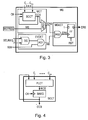
- FIG. 3 represents an exemplary embodiment of the security device MU. This includes an MCT error detection circuit, an EVDET event detection circuit, and an error mode masking circuit MSKCT.
- MCT error detection circuit an EVDET event detection circuit
- MSKCT error mode masking circuit
- the error detection circuit MCT monitors the progress of the execution of a command and provides, from the beginning of the execution of the command, an internal error signal ERS 'which presents an active state representative of the mode of operation. error, and an inactive state representative of the lifting of the error mode.
- the circuit MCT comprises a wired logic SCCT signature calculation circuit receiving, on parallel inputs, deterministic logic signals C i to C i + n .
- These signals C i to C i + n are selected here from the control signals C 1 to C m provided by the control block FSM (FIG. 2) and are deterministic (predictable) in that they depend only on the command that executes the coprocessor.
- the SCCT circuit has an output that is returned to one of its inputs and provides a current cumulative signature CCS. Every signature The cumulative current CCS is thus a function of the signals C i to C i + n and of a previous cumulative signature.
- the calculation of the signatures is carried out at the rate of a clock signal, for example the clock signal CK of the CPU.
- the current cumulative signature CCS is applied to an input of a comparator COMP whose other input receives an expected signature WS.
- the comparator has an inverting output which provides the internal error signal ERS 'so that it remains equal to 1 (active state, error mode) as long as the current calculated signature CCS is different from the expected signature WS .
- the error mode is also maintained when the processing of the command is finished, if a runtime error has been detected (because the expected signature is not obtained).
- the expected signature WS is stored in any storage means, here an additional register REFREG of the coprocessor to which the circuit MCT is connected (Fig. 2 and Fig. 3).
- This signature being a function of the command to be executed, it can be registered in the REFREG register by the CPU itself before activating the coprocessor (triggered by the positioning of the RUN bit).
- the means for storing the signature WS may be a table or a set of coprocessor registers in which are prerecorded various expected signatures each corresponding to a command of a set of commands of the coprocessor. In this case, one of the expected signatures is selected in the table or in one of the specific registers when a command is loaded in the COMREG register.
- the EVDET event detection circuit provides an RR signal that is in the active state when the monitored event is detected, here an attempt to read a coprocessor register.
- it comprises a gate OG of type OR with several inputs and a gate AG1 of type ET with two inputs.
- the gate OG receives the selection signals SELREG i from the coprocessor registers whose read access is to be monitored, and its output goes to 1 when one of the registers under surveillance is selected by the address decoder ADDEC (FIG. 2).
- the output of the gate OG is applied to an input of the gate AG1 whose other input receives the signal R / W described above and whose output provides the signal RR.
- the R / W signal here being conventionally equal to 1 for read access, the RR signal goes to 1 (active value) when an attempt to read access to certain registers is detected.
- the masking circuit MSKCT receives the internal error signal ERS 'and the detection signal RR, and provides the external error signal ERS.
- the ERS signal is in the active state when the error mode is declared in the middle outside the coprocessor (here the CPU), and the inactive state when the error mode is hidden.
- the circuit MSKCT comprises an AND type gate AG2 receiving on its inputs the signal ERS 'and the signal RR, and supplying the external error signal ERS.
- the internal error signal ERS ' is at 1 (active value, error mode) the ERS signal remains at 0 (error mode masked) as long as the RR signal is at 0 (no detection of an attempt to read access to a registry under surveillance).
- the switching of the ERS error signal from the inactive state to the active state is preferably stored by the circuit MSKCT. This storage is ensured here by a flip-flop FF comprising an input D, a non-inverting output Q and a clock input H.
- the logic value 1 is permanently applied to the input D, the external error signal ERS is applied at the entrance H and is recovered on the output Q to be sent to the outside environment.
- the change to 1 of the error signal ERS causes the output Q to change to 1, which copies the input D.
- the error signal ERS is stably copied when the error signal ERS on the H entry passes to 1 fugitively following an attempt to access a registry under surveillance while the expected signature WS is not yet reached or has not been reached at the end of the execution of the command.
- the flip-flop FF receives a reset signal RST which is activated after the error has been processed.
- the calculated signature is different from the expected value and the coprocessor is by default in the error mode. If a read attempt is made on one of the monitored registers during the execution time of the command, the error mode is declared by carrying the external error signal ERS to its active value.
- the calculated signature is normally equal to the expected signature, the coprocessor then leaves the error mode. In the opposite case, the signature calculated at the end of processing is different from the expected signature and the error mode is not raised. Any attempt access to a register under surveillance then triggers the transition to the active state of the external error signal ERS, despite the fact that the execution of the command is completed.
- the transition of the external ERS error signal to the active state causes a CPU shutdown or reset or any other emergency measure known to those skilled in the art.
- the CPU must detect the end of the processing performed by the coprocessor by periodically reading the STATREG status register, it must be able to access the STATREG register without this activating the external error signal.
- the selection signal SELREG i corresponding to this register must not be applied to the detection circuit EVDET.
- the SCCT signature calculation circuit is, for example, a Linear Feedback Shift Register (LSFR).
- I1 comprises a logic circuit PLCT and a signature register SREG with input and output of parallel type.
- the circuit PLCT executes a signature function Fs and comprises inputs receiving the control signals C i to C i + n and an input receiving a current cumulative signature CCS.
- the MU security device has been described as a separate element of the FSM control block, it can be integrated into the control block and additional functions can be provided in connection with the control unit. security.
- the block FSM is arranged to check that the internal error signal ERS 'is at the active value before initiating the execution of a command. If this is not the case, the FSM block forces the external ERS error signal to the active value and places itself in a specific state from which it can only exit after a complete reset of the coprocessor.
- the logic values described above corresponding to the active state of the error signals ERS ', ERS have only a relative value. Other values can be retained, for example the value "1" for the active state of the internal error signal ERS 'and the value "0" for the active state of the external error signal ERS.
- the signal ERS must be set to 0 when the signal ERS 'is at 1, since it is not the logical value which is copied but the active or inactive state of the internal error signal which is associated by convention a logic value that may be different for the internal error signal and for the external error signal.
- a security device making it possible to carry the coprocessor by default in an error mode, and to declare the mode of error in the external environment when the conditions described above are met.
- the security device MU can act on specific flags (flags) provided in the STATREG status register of the coprocessor, such as a flag representative of the error mode and a flag indicating whether the event to be monitored has been detected. .
- An alarm device external to the coprocessor can be assigned to the permanent surveillance or not of these flags and itself issue the external error signal.
- This external device can also be programmable according to several levels of security, to conduct or trigger specific actions when the error conditions are met, according to a security level that has been communicated to it by the CPU.
- control of the smooth running of the execution of the command can also be carried out in various ways, for example by applying the control techniques mentioned in the preamble, based on a redundancy of the data paths present in the coprocessor calculation unit. or by combining such technique with that based on deterministic signal function generation.
- the event to be monitored may consist of any type of event in connection with an attempted fraud, and is not necessarily an attempt to read a register and the identification of events to be monitored depends of course on the architecture of the coprocessor and the operations entrusted to it. It may be an attempt to write a register, an attempt to access a coprocessor member, and generally an action from outside the coprocessor and concerning the coprocessor.
- the event may also be unrelated to an attempted fraud, and simply be an event whose occurrence is certain after the processing of an order, such as stopping the process of executing the order itself.
- an event is used to declare the error mode to the outside environment, by analogy it serves as a "trigger" for the security system according to the invention, which is “armed” from the beginning of the execution of the the command.
- coprocessor in the sense of the invention to be understood in a non-limiting way.
- a coprocessor within the meaning of the invention is a wired logic circuit designed to perform specific operations in response to a command supplied to it.
- wired logic circuits that provide data bus control or address in microprocessors or microcontrollers or that control access to memories.
Landscapes
- Engineering & Computer Science (AREA)
- Theoretical Computer Science (AREA)
- Quality & Reliability (AREA)
- Physics & Mathematics (AREA)
- General Engineering & Computer Science (AREA)
- General Physics & Mathematics (AREA)
- Advance Control (AREA)
- Microcomputers (AREA)
- Hardware Redundancy (AREA)
- Debugging And Monitoring (AREA)
Applications Claiming Priority (1)
| Application Number | Priority Date | Filing Date | Title |
|---|---|---|---|
| FR0503331A FR2883998A1 (fr) | 2005-04-05 | 2005-04-05 | Coprocesseur securise comprenant un circuit de detection d'un evenement |
Publications (2)
| Publication Number | Publication Date |
|---|---|
| EP1772805A2 true EP1772805A2 (de) | 2007-04-11 |
| EP1772805A3 EP1772805A3 (de) | 2010-05-19 |
Family
ID=35079442
Family Applications (1)
| Application Number | Title | Priority Date | Filing Date |
|---|---|---|---|
| EP06003810A Withdrawn EP1772805A3 (de) | 2005-04-05 | 2006-02-24 | Sicherer Co-Prozessor mit Schaltung für Ereignisdetektion |
Country Status (3)
| Country | Link |
|---|---|
| US (2) | US7954153B2 (de) |
| EP (1) | EP1772805A3 (de) |
| FR (1) | FR2883998A1 (de) |
Families Citing this family (13)
| Publication number | Priority date | Publication date | Assignee | Title |
|---|---|---|---|---|
| CN101689233B (zh) * | 2007-07-05 | 2013-01-02 | Nxp股份有限公司 | 安全敏感系统中的微处理器 |
| US8281229B2 (en) * | 2008-12-30 | 2012-10-02 | Intel Corporation | Firmware verification using system memory error check logic |
| US8621116B2 (en) | 2011-08-26 | 2013-12-31 | Lexmark International, Inc. | Dynamic address change optimizations |
| US8225021B2 (en) * | 2009-05-28 | 2012-07-17 | Lexmark International, Inc. | Dynamic address change for slave devices on a shared bus |
| WO2013012436A1 (en) | 2011-07-18 | 2013-01-24 | Hewlett-Packard Development Company, L.P. | Reset vectors for boot instructions |
| US9032258B2 (en) * | 2012-09-14 | 2015-05-12 | Infineon Technologies Ag | Safety system challenge-and-response using modified watchdog timer |
| DE102012108981A1 (de) * | 2012-09-24 | 2014-03-27 | Infineon Technologies Ag | Ein-/Ausgabe-Modul, Datenverarbeitungsvorrichtung und Verfahren zum Überprüfen der Funktion einer Datenverarbeitungsvorrichtung |
| US9223983B2 (en) * | 2013-03-15 | 2015-12-29 | Intel Corporation | Security co-processor boot performance |
| US9817670B2 (en) | 2013-12-13 | 2017-11-14 | International Business Machines Corporation | Framework to provide time bound execution of co-processor commands |
| GB2531586A (en) * | 2014-10-23 | 2016-04-27 | Ibm | Methods and systems for starting computerized system modules |
| US9934377B2 (en) | 2015-11-20 | 2018-04-03 | Atmel Corporation | Input/output parameter selection |
| WO2017155598A2 (en) * | 2016-01-05 | 2017-09-14 | Philip Koopman | A safety architecture for autonomous vehicles |
| US11693696B2 (en) * | 2020-09-11 | 2023-07-04 | EMC IP Holding Company LLC | Techniques for command execution using a state machine |
Citations (1)
| Publication number | Priority date | Publication date | Assignee | Title |
|---|---|---|---|---|
| FR2746199A1 (fr) | 1996-03-11 | 1997-09-19 | Vlsi Technology Inc | Architecture de securite a double fonction avec systeme d'exploitation interne protege |
Family Cites Families (34)
| Publication number | Priority date | Publication date | Assignee | Title |
|---|---|---|---|---|
| JPS61278992A (ja) * | 1985-06-04 | 1986-12-09 | Toppan Moore Co Ltd | 故障検査機能を備えたicカ−ド |
| US4996691A (en) * | 1988-09-21 | 1991-02-26 | Northern Telecom Limited | Integrated circuit testing method and apparatus and integrated circuit devices for use therewith |
| JP2617026B2 (ja) * | 1989-12-22 | 1997-06-04 | インターナショナル・ビジネス・マシーンズ・コーポレーション | 障害余裕性メモリ・システム |
| US5184032A (en) * | 1991-04-25 | 1993-02-02 | Texas Instruments Incorporated | Glitch reduction in integrated circuits, systems and methods |
| US5148032A (en) * | 1991-06-28 | 1992-09-15 | Siemens Medical Laboratories, Inc. | Radiation emitting device with moveable aperture plate |
| US5357146A (en) * | 1992-12-31 | 1994-10-18 | At&T Bell Laboratories | Glitch-free clock multiplexer |
| US5435001A (en) * | 1993-07-06 | 1995-07-18 | Tandem Computers Incorporated | Method of state determination in lock-stepped processors |
| JP2783243B2 (ja) * | 1996-02-06 | 1998-08-06 | 日本電気株式会社 | Cmos集積回路の故障検出方法及び装置 |
| JP3625340B2 (ja) | 1996-09-19 | 2005-03-02 | 株式会社東芝 | セキュリティシステム |
| US5694402A (en) * | 1996-10-22 | 1997-12-02 | Texas Instruments Incorporated | System and method for structurally testing integrated circuit devices |
| JP2982741B2 (ja) * | 1997-05-13 | 1999-11-29 | 日本電気株式会社 | 集積回路の故障診断装置及びその記録媒体 |
| US6278782B1 (en) * | 1997-09-16 | 2001-08-21 | Safenet, Inc. | Method of implementing a key recovery system |
| AU1699499A (en) * | 1997-11-17 | 1999-06-07 | Lifestyle Technologies | Universal power supply |
| US5974529A (en) * | 1998-05-12 | 1999-10-26 | Mcdonnell Douglas Corp. | Systems and methods for control flow error detection in reduced instruction set computer processors |
| SE512916C2 (sv) * | 1998-07-16 | 2000-06-05 | Ericsson Telefon Ab L M | Metod och anordning för feldetektering i digitalt system |
| US6357024B1 (en) * | 1998-08-12 | 2002-03-12 | Advanced Micro Devices, Inc. | Electronic system and method for implementing functional redundancy checking by comparing signatures having relatively small numbers of signals |
| FR2790844B1 (fr) * | 1999-03-09 | 2001-05-25 | Gemplus Card Int | Procede et dispositif de surveillance du deroulement d'un programme, dispositif programme permettant la surveillance de son programme |
| EP1087233A1 (de) * | 1999-09-23 | 2001-03-28 | Infineon Technologies AG | Verfahren und Anordnung zum datenschützenden Selbsttest für Microcontroller |
| JP3371865B2 (ja) * | 1999-09-27 | 2003-01-27 | 日本電気株式会社 | 集積回路の故障検査装置、故障検査方法、及び故障検査制御プログラムを記録した記録媒体 |
| JP3734392B2 (ja) * | 1999-10-29 | 2006-01-11 | 松下電器産業株式会社 | 半導体集積回路の故障検査方法及びレイアウト方法 |
| US6424926B1 (en) * | 2000-03-31 | 2002-07-23 | Intel Corporation | Bus signature analyzer and behavioral functional test method |
| US6714032B1 (en) * | 2000-04-25 | 2004-03-30 | Agere System Inc. | Integrated circuit early life failure detection by monitoring changes in current signatures |
| US6799287B1 (en) * | 2000-05-01 | 2004-09-28 | Hewlett-Packard Development Company, L.P. | Method and apparatus for verifying error correcting codes |
| US6549022B1 (en) * | 2000-06-02 | 2003-04-15 | Sandia Corporation | Apparatus and method for analyzing functional failures in integrated circuits |
| US6751749B2 (en) * | 2001-02-22 | 2004-06-15 | International Business Machines Corporation | Method and apparatus for computer system reliability |
| US6571317B2 (en) * | 2001-05-01 | 2003-05-27 | Broadcom Corporation | Replacement data error detector |
| US6601008B1 (en) * | 2001-08-02 | 2003-07-29 | Lsi Logic Corporation | Parametric device signature |
| US7185249B2 (en) * | 2002-04-30 | 2007-02-27 | Freescale Semiconductor, Inc. | Method and apparatus for secure scan testing |
| KR100440451B1 (ko) * | 2002-05-31 | 2004-07-14 | 삼성전자주식회사 | 전압 글리치 검출 회로, 그것을 구비하는 집적회로장치,그리고 전압 글리치 어택으로부터 집적회로장치를보호하는 장치 및 방법 |
| US7383587B2 (en) * | 2002-11-18 | 2008-06-03 | Arm Limited | Exception handling control in a secure processing system |
| JP2005203064A (ja) * | 2004-01-19 | 2005-07-28 | Toshiba Corp | 半導体記憶装置 |
| US7328377B1 (en) * | 2004-01-27 | 2008-02-05 | Altera Corporation | Error correction for programmable logic integrated circuits |
| ES2279308T3 (es) * | 2004-06-01 | 2007-08-16 | France Telecom | Control de acceso a una red de un terminal fuente que utiliza un tunel en modo bloqueante. |
| US20060267653A1 (en) * | 2005-05-25 | 2006-11-30 | Honeywell International Inc. | Single-event-effect hardened circuitry |
-
2005
- 2005-04-05 FR FR0503331A patent/FR2883998A1/fr active Pending
-
2006
- 2006-02-24 EP EP06003810A patent/EP1772805A3/de not_active Withdrawn
- 2006-04-05 US US11/398,850 patent/US7954153B2/en not_active Expired - Fee Related
-
2011
- 2011-04-19 US US13/090,140 patent/US8359481B2/en active Active
Patent Citations (1)
| Publication number | Priority date | Publication date | Assignee | Title |
|---|---|---|---|---|
| FR2746199A1 (fr) | 1996-03-11 | 1997-09-19 | Vlsi Technology Inc | Architecture de securite a double fonction avec systeme d'exploitation interne protege |
Also Published As
| Publication number | Publication date |
|---|---|
| US7954153B2 (en) | 2011-05-31 |
| US8359481B2 (en) | 2013-01-22 |
| US20110214012A1 (en) | 2011-09-01 |
| US20060259673A1 (en) | 2006-11-16 |
| EP1772805A3 (de) | 2010-05-19 |
| FR2883998A1 (fr) | 2006-10-06 |
Similar Documents
| Publication | Publication Date | Title |
|---|---|---|
| EP1772805A2 (de) | Sicherer Co-Prozessor mit Schaltung für Ereignisdetektion | |
| EP2280364B1 (de) | Fehlerinjektionsdetektor in einer integrierten Schaltung | |
| EP1605333B1 (de) | Programmausführungssteuerung | |
| FR2790844A1 (fr) | Procede et dispositif de surveillance du deroulement d'un programme, dispositif programme permettant la surveillance de son programme | |
| EP1748374A1 (de) | Verfahren und Vorrichtung zum Schutz eines Speichers gegen Angriffe mittels Fehlerinjektion | |
| EP1710700A2 (de) | Sicherer Co-Prozessor mit Mitteln zur Verhinderung des Zugriffs auf einer Co-prozessoreinheit | |
| EP1108249B1 (de) | Absicherungsverfahren für die bearbeitung einer sicherheitsrelevanten information in einem monolitischen sicherheitsmodul, und entsprechendes sicherheitsmodul | |
| EP2158557B1 (de) | Verfahren und vorrichtung für den nachweis von fehlersprüngen während der ausfühurung eines programms | |
| EP1939745B1 (de) | Verfahren und Vorrichtung zur Sicherung vom Speicherszugang | |
| EP1821111B1 (de) | Elektronischer Schaltkreis, der einen mittels Verwendung eines Identifikators gesicherten Testmodus umfasst, und zugehöriges Verfahren | |
| FR2757972A1 (fr) | Procede de securisation d'un module de securite, et module de securite associe | |
| FR2903497A1 (fr) | Circuit electronique comprenant un mode de test securise par insertion de donnees leurres dans la chaine de test,procede associe. | |
| FR2889005A1 (fr) | Integrite materielle permanente des donnees | |
| EP1950577A2 (de) | Verfahren zur Integritätsüberprüfung einer Uhrwerkswelle | |
| EP1717704A2 (de) | Schutz des Ablaufs eines von einem integrierten Schaltkreis ausgeführten Programms | |
| EP3042334B1 (de) | Verfahren zur installation einer sicherheitsvorrichtung in abhängigkeit einen vertrauensindex in einer elektronischen vorrichtung mit speicher und vorrichtung zur durchführung des verfahrens | |
| EP1589394B1 (de) | Mikroprozessor mit Mitteln zur Detektion von Fehlern, immunisiert gegen einen Fehlerinjektionsangriff | |
| EP1589395B1 (de) | Mikroprozessor mit Signaturmitteln zur Detektion eines Fehlerinjektionsangriffes | |
| EP2229648B1 (de) | Verfahren zur sicheren datenübertragung | |
| EP0463901B1 (de) | Dialogverfahren zwischen den Prozessoren eines Systems, System zu seiner Durchführung und zu seinem Einsatz für die Verteilung von Prozessen auf Prozessoren | |
| EP1742075B1 (de) | Verfahren zum Testen eines elektronischen Schaltkreises, das einen mittels Verwendung einer Signatur gesicherten Testmodus umfasst, und zugehöriger elektronischer Schaltkreis | |
| EP1942428B1 (de) | Verfahren zur Konformitätsprüfung einer elektronischen Plattform und/oder eines Softwareprogramms auf dieser Plattform sowie entsprechende Vorrichtung und entsprechendes Computerprogramm | |
| FR3140186A1 (fr) | Procédé de détection d’une tentative d’extraction linéaire du contenu d’une mémoire | |
| WO2016181062A1 (fr) | Procede de securisation d'une comparaison de donnees lors de l'execution d'un programme | |
| WO2023083776A1 (fr) | Procédé de détection d'une tentative d'extraction linéaire du contenu d'une mémoire |
Legal Events
| Date | Code | Title | Description |
|---|---|---|---|
| PUAI | Public reference made under article 153(3) epc to a published international application that has entered the european phase |
Free format text: ORIGINAL CODE: 0009012 |
|
| AK | Designated contracting states |
Kind code of ref document: A2 Designated state(s): AT BE BG CH CY CZ DE DK EE ES FI FR GB GR HU IE IS IT LI LT LU LV MC NL PL PT RO SE SI SK TR |
|
| AX | Request for extension of the european patent |
Extension state: AL BA HR MK YU |
|
| PUAL | Search report despatched |
Free format text: ORIGINAL CODE: 0009013 |
|
| AK | Designated contracting states |
Kind code of ref document: A3 Designated state(s): AT BE BG CH CY CZ DE DK EE ES FI FR GB GR HU IE IS IT LI LT LU LV MC NL PL PT RO SE SI SK TR |
|
| AX | Request for extension of the european patent |
Extension state: AL BA HR MK YU |
|
| 17P | Request for examination filed |
Effective date: 20101108 |
|
| AKX | Designation fees paid |
Designated state(s): DE FR GB IT |
|
| 17Q | First examination report despatched |
Effective date: 20110405 |
|
| STAA | Information on the status of an ep patent application or granted ep patent |
Free format text: STATUS: THE APPLICATION IS DEEMED TO BE WITHDRAWN |
|
| 18D | Application deemed to be withdrawn |
Effective date: 20120830 |