EP1770866A1 - High-speed analog/digital converter - Google Patents
High-speed analog/digital converter Download PDFInfo
- Publication number
- EP1770866A1 EP1770866A1 EP05019801A EP05019801A EP1770866A1 EP 1770866 A1 EP1770866 A1 EP 1770866A1 EP 05019801 A EP05019801 A EP 05019801A EP 05019801 A EP05019801 A EP 05019801A EP 1770866 A1 EP1770866 A1 EP 1770866A1
- Authority
- EP
- European Patent Office
- Prior art keywords
- detection means
- difference detection
- analog
- digital converter
- current sources
- Prior art date
- Legal status (The legal status is an assumption and is not a legal conclusion. Google has not performed a legal analysis and makes no representation as to the accuracy of the status listed.)
- Granted
Links
Images


Classifications
-
- H—ELECTRICITY
- H03—ELECTRONIC CIRCUITRY
- H03M—CODING; DECODING; CODE CONVERSION IN GENERAL
- H03M1/00—Analogue/digital conversion; Digital/analogue conversion
- H03M1/06—Continuously compensating for, or preventing, undesired influence of physical parameters
Definitions
- the reference ladder implementation most commonly described is depicted in Fig. 1.
- the input voltage vin is applied to one input of each differential amplifier.
- the other amplifier input is connected to the reference voltage produced by a chain of equal resistors R.
- Two reference voltages Vmin and Vmax are applied to the endpoints of the chain. They define the boundaries of the reference voltage range. Intermediate nodes of the chain will settle to linearly spaced intermediate voltages, to the extent that the differential amplifier inputs draw only negligible current.
- the differential amplifiers are implemented using bipolar transistors in the input stage, they draw a substantial signal-dependent DC input current, which tends to distort the distribution of reference voltages.
- the value of resistors R must be chosen small enough that the DC current through the chain is much larger than the input currents of the differential amplifiers. This sensitivity to amplifier input currents is a drawback of this circuit.
- the other drawback is that the circuit is single-ended. It is possible to obtain a pseudo-differential version of this circuit by combining two of them, but this solution does not lead to a reduction in input signal swing because one input of each differential amplifier remains a DC voltage.
- the intermediate signals are identical to Vinp and vinn except for a DC offset determined by R and Iref.
- the two inputs of each differential amplifier vary in a complementary fashion. Thereby, for a same differential input voltage range seen at the amplifier inputs, the voltage swing at inputs vinp and vinn is a factor of two smaller than in the previous circuit. This feature enables significant reduction of nonlinear distortion if the input signal amplitude would otherwise cause the active devices to operate near the limit of their breakdown voltage.
- a substantial drawback of the differential reference ladder circuit shown in Fig. 2 is that the input signal must propagate down a chain of resistors. Because of the input capacitance of the differential amplifiers, the signal gets delayed and low-pass filtered as it travels down the chain. The delay from the input to each differential amplifier output depends on the number of resistors on the signal path to this particular amplifier. Thereby, the delay between the positive and the negative side of a same differential amplifier cannot be well matched. Also, skew between the outputs of different amplifiers is unavoidable. For these reasons, the above circuit cannot be used in practice for very high-speed ADC.
- the difference of the currents of the first current sources, and the second current sources increases or decreases linearly from difference detection means to difference detection means.
- the currents generated by the first and second current sources are integer multiples of a reference current.
- the reference currents of the first current sources and the reference currents of the second current sources are identical.
- first current sources generating a current differing form zero are only connected to the positive input ports of a first set of difference detection means and second current sources generating a current differing from zero are only connected to the negative input ports of a second set of difference detection means, whereby the first set and the second set do not comprise any identical difference detection means.
- current sources generating a current differing from zero are connected to positive input ports only or to negative input ports of the difference detection means only.
- the delays between the inputs and all differential amplifier outputs are essentially identical because the same series resistance and parasitic load capacitance is seen by the signal on all paths.
- the reference voltages are not sensitive to the input bias currents of the differential amplifiers. Indeed, around a zero-crossing, the input bias current will be essentially identical at both inputs of the differential amplifier, therefore the voltage drop across the resistances will be identical on both sides. This effect has impact only on the common-mode input voltage, not the differential voltage.
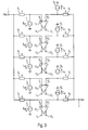
- a first embodiment of a reference ladder circuit is shown in Fig. 3.
- five difference detection means are used in the reference ladder implementation, however, in principle any number can be used.
- a resistor is inserted in the signal path between the input voltages - vinp and vinn - and each differential amplifier input. It is best if all resistors have the same value R, so that the delays across all signal paths will be essentially the same.
- a DC reference current is drawn at each differential amplifier input, thereby causing a DC voltage drop across the related resistor.
- the zero-crossing of each differential amplifier will be shifted by an offset voltage proportional to R and to the difference between the reference currents drawn at the positive and the negative inputs of the differential amplifier.
- the most straightforward choice is to use linearly spaced reference currents.
- 5 and 6 may be suitably represented in matrix representation: 4 0 2 0 0 0 0 2 0 4 o ⁇ r ( - 2 2 - 1 1 0 0 1 - 1 2 - 2 ) o ⁇ r ( 0 - 4 0 - 2 0 0 0 2 0 4 ) where the left hand side of each matrix represents the left hand side current sources in Fig. 3 and the right hand side of the matrix represents the right hand side of the current sources in Fig. 3.
- the threshold of a differential amplifier is shifted by R ⁇ (I pk - I nk ).
- the circuit has two input terminals referenced with 1 and 2. These input terminals can be connected to the positive and negative voltage Vinp and Vinn of an input line carrying a differential signal.
- Resistors 3 1 , 3 2 , 3 3 , 3 4 , 3 5 as well as current sources 7 1 , 7 2 , 7 3 , 7 4 , 7 5 are connected to first input ports 9 1 , 9 2 , 9 3 , 9 4 , 9 5 of difference detection means 13 1 , 13 2 , 13 3 , 13 4 , 13 5 , respectively.
- a detected difference can be tapped at output ports 11 1 , 11 2 , 11 3 , 11 4 , 11 5 of difference detection means 13 1 , 13 2 , 13 3 , 13 4 , 13 5 , respectively.
- the difference detection means 13 1 -13 5 detect a voltage difference between its input ports 9 1 , 10 1 ; 9 2 , 10 2 ; 9 3 , 10 3 ; 9 4 , 10 4 and 9 5 , 10 5 , respectively.
- the detection means can be a comparator or a differential amplifier.
- the currents of first current sources 7 1 , 7 2 , 7 3 , 7 4 , 7 5 as shown in subsequently explained embodiment of Fig. 4 are integer multiples of Iref.
- the currents are 0, Iref, 2Iref, 3Iref, and 4Iref generated by the current sources 7 1 , 7 2 , 7 3 , 7 4 , 7 5 , respectively.
- the voltage drops across resistors 3 1 , 3 2 , 3 3 , 3 4 , and 3 5 are 0, R ⁇ Iref, R ⁇ 2 ⁇ Iref, R ⁇ 3 ⁇ Iref, and R ⁇ 4 ⁇ Iref.
- the difference detection means obtain a voltage: 0, Vinp, Vinp - R ⁇ Iref, Vinp - R ⁇ 2 ⁇ Iref, Vinp - R ⁇ 3 ⁇ Iref, Vinp - R ⁇ 4 ⁇ Iref.
- Resistors 4 1 , 4 2 , 4 3 , 4 4 , 4 5 of the analog-to-digital-converter are connected to input terminal 2 on one side.
- Second resistors 4 1 , 4 2 , 4 3 , 4 4 , 4 5 as well as second current sources 8 1 , 8 2 , 8 3 , 8 4 , 8 5 are connected to the second (negative) input ports 10 1 , 10 2 , 10 3 , 10 4 , 10 5 of difference detection means 13 1 , 13 2 , 13 3 , 13 4 , 13 5 , respectively.
- the currents of second current sources 8 1 , 8 2 , 8 3 , 8 4 , and 8 5 are also integer multiples of Iref.
- the currents of second current sources 8 1 , 8 2 , 8 3 , 8 4 , 8 5 are 4Iref, 3Iref, 2Iref, Iref, and 0, respectively, and increase in reverse order as their counterparts connected to the first input ports 9 1 , 9 2 , 9 3 , 9 4 , and 9 5 .
- the voltage drops across resistors 4 1 , 4 2 , 4 3 , 4 4 , and 4 5 are consequently R ⁇ 4Iref, R ⁇ 3Iref, R ⁇ 2 Iref, R ⁇ Iref, and 0.
- the difference detection means 13 1 , 13 2 , 13 3 , 13 4 , and 13 5 obtain a voltage: Vinn - R ⁇ 4Iref, Vinn - R ⁇ 3Iref, Vinn - R ⁇ 2Iref, Vinn - R ⁇ 3Iref, Vinn.
- the current of the current sources which operate actually as current sinks is supplied via the input terminals Vinp and Vinn through a suitable driving circuit, such as an emitter follower.
- a suitable driving circuit such as an emitter follower.
- Iref does not strictly need to be tuned to a current magnitude that is large with respect to the input currents of the difference detection means.
- a difference detection means will provide information on the voltage level when the voltage at both inputs, e.g. inputs 9 3 and 10 3 , are almost equal. At this instance the input currents of both, the first and the second input terminal, are also equal, so that the voltage difference is not affected.
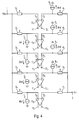
- Fig. 4 illustrates the sample circuit where the current magnitudes k ⁇ Iref are distributed in the manner that k starts from 0 incrementing up to 4 from difference detection means 13 1 towards difference detection means 13 5 for the left hand side current sources 7 1 to 7 5 in Fig. 3 and decrementing from 4 down to 0 for the right hand side sources 8 1 to 8 5 in Fig. 3.
- the arrangement of the resistors 3 1 , 3 2 , 3 3 , 3 4 , and 3 5 has not changed in that they are still connected on one side with the positive input terminal 1 and on the other side with the positive input port 9 1 to 9 5 of the difference detection means 13 1 to 13 5 .
- resistors 4 1 to 4 5 are connected on one side with the negative input ports 10 1 to 10 5 and on the other side with negative input terminal 2.
- the current sources with currents of 0 have been left out of the drawing.
- differential offset voltages L ⁇ R ⁇ Iref, with L ⁇ ⁇ -4, -2, 0, 2, 4 ⁇ are obtained which provide a linear distribution of the differential voltages.
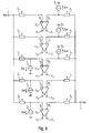
- Fig. 5 shows an embodiment where the currents of the left hand side current sources 7 1 to 7 5 of Fig. 3 are all set to zero and the right hand side current sources 8 1 to 8 5 provide currents that correspond to the differential offset voltages of the circuit shown in Figure 4.
- the matrix representation of the current distribution is 0 - 4 0 - 2 0 0 0 2 0 4 in this case.
- Fig. 6 shows an embodiment of the invention analog-to-digital converter with an asymmetric distribution of the current sources.
- current sources with a current of 0 are left out and the corresponding matrix representation can be given as: ( 0 4 0 2 0 0 2 0 4 0 ) .
- the invention is not restricted to the above embodiments and can be used with different implementations.
- the current sources and the input stages of the differential amplifiers can be implemented in bipolar technology but also in CMOS technology.
- the current sources can be configured as current mirror circuits. All features described in this description and shown in the accompanying drawings can be combined.
Landscapes
- Engineering & Computer Science (AREA)
- Theoretical Computer Science (AREA)
- Analogue/Digital Conversion (AREA)
- Amplifiers (AREA)
Abstract
Description
- Many common analog/digital converter (ADC) architectures, notably Flash converters and Folding & Interpolating converters include a circuit stage - called reference ladder in the present document - comparing an analog input voltage to a set of constant reference voltages. The constant reference voltages are typically linearly spaced across the input voltage range supported by the ADC. The reference ladder typically includes a circuit generating the reference voltages and a set of differential amplifiers computing the differences between an input voltage and each reference voltage.
- The present document describes a novel reference ladder circuit presenting the following advantages:
- (a) The input signal propagates to the outputs of all differential amplifiers with essentially the same delay.
- (b) The implementation is fully differential.
- (c) The reference voltages are not perturbed by the input bias current of the differential amplifiers.
- None of the reference ladder implementations published so far possesses all of these properties. Indeed, at the sampling rates and resolutions where existing ADC chips operate, satisfactory ADC performance can be achieved even if the reference ladder lacks some of these features. However, as sampling rates increase well above 1 GS/s, the above features become increasingly necessary for the following reasons:
- (a) Delay mismatch (a.k.a. skew) between differential amplifier outputs must remain a small fraction of the sampling period.
- (b) As sampling rates increase, delay matching specifications become increasingly stringent. As transistors become faster, their breakdown voltage tends to decrease. Therefore, ADC implementations pushing the speed limit must operate with ever smaller signal swings. A fully differential architecture reduces the voltage swing seen by a differential amplifier input by half compared to a single-ended or pseudo-differential architecture.
- The reference ladder implementation most commonly described is depicted in Fig. 1. The input voltage vin is applied to one input of each differential amplifier. The other amplifier input is connected to the reference voltage produced by a chain of equal resistors R. Two reference voltages Vmin and Vmax are applied to the endpoints of the chain. They define the boundaries of the reference voltage range. Intermediate nodes of the chain will settle to linearly spaced intermediate voltages, to the extent that the differential amplifier inputs draw only negligible current.
- In practice, if the differential amplifiers are implemented using bipolar transistors in the input stage, they draw a substantial signal-dependent DC input current, which tends to distort the distribution of reference voltages. In order to minimize this effect, the value of resistors R must be chosen small enough that the DC current through the chain is much larger than the input currents of the differential amplifiers. This sensitivity to amplifier input currents is a drawback of this circuit.
- The other drawback is that the circuit is single-ended. It is possible to obtain a pseudo-differential version of this circuit by combining two of them, but this solution does not lead to a reduction in input signal swing because one input of each differential amplifier remains a DC voltage.
- A truly differential reference ladder implementation has been described in J. Lee, P. Roux, U.V. Koc, T. Link, Y. Baeyens, Y.K. Chen, "A 5 - b 10 - GSample/s A/D Converter for 10 - Gb/s Optical Receivers", IEEE Journal of Solid-State Circuits, Vol. 39, No. 10, Oct. 2004, pp. 1671 - 1679. This circuit is shown in Fig. 2. Input vinp is the positive side and vinn the negative side of a differential input voltage. By means of two chains of resistors R across which flows a reference current Iref, a number of intermediate signals are obtained. The intermediate signals are identical to Vinp and vinn except for a DC offset determined by R and Iref. In this circuit, the two inputs of each differential amplifier vary in a complementary fashion. Thereby, for a same differential input voltage range seen at the amplifier inputs, the voltage swing at inputs vinp and vinn is a factor of two smaller than in the previous circuit. This feature enables significant reduction of nonlinear distortion if the input signal amplitude would otherwise cause the active devices to operate near the limit of their breakdown voltage.
- A substantial drawback of the differential reference ladder circuit shown in Fig. 2 is that the input signal must propagate down a chain of resistors. Because of the input capacitance of the differential amplifiers, the signal gets delayed and low-pass filtered as it travels down the chain. The delay from the input to each differential amplifier output depends on the number of resistors on the signal path to this particular amplifier. Thereby, the delay between the positive and the negative side of a same differential amplifier cannot be well matched. Also, skew between the outputs of different amplifiers is unavoidable. For these reasons, the above circuit cannot be used in practice for very high-speed ADC.
- It can be shown that input bias currents of the differential amplifier will affect the accuracy and linearity of the above reference ladder circuit to a similar extent as the circuit in Fig. 1.
- It is the object of the present invention to provide a high speed analog/digital converter being suitable for differential signals and working with a very high accuracy.
- The object is solved by the features of
claim 1. The dependent claims comprise further developments of the invention. - According to the invention the analog-to-digital converter comprises a positive input terminal, a negative input terminal, several difference detection means detecting a voltage difference between a positive input port and a negative input port, first resistors connecting each positive input port of each difference detection means with the positive input terminal and second resistors connecting each negative input port of each difference detection means with the negative input terminal. First current sources are connected to the positive input port of at least some of the difference detection means generating different currents. Second current sources are connected to the negative input port of at least some of the difference detection means also generating different currents.
- Preferably the difference of the currents of the first current sources, and the second current sources increases or decreases linearly from difference detection means to difference detection means.
- Alternatively the difference of the currents of the first current sources and the second current sources increases or decreases nonlinearly from difference detection means to difference detection means.
- Preferably the first resistors and the second resistors have equal resistances.
- Preferably the sums of currents of the first and second current sources that are connected to the same difference detection means are equal for each difference detection means.
- Preferably the currents generated by the first and second current sources are integer multiples of a reference current.
- Preferably the reference currents of the first current sources and the reference currents of the second current sources are identical.
- Preferably first current sources generating a current differing form zero are only connected to the positive input ports of a first set of difference detection means and second current sources generating a current differing from zero are only connected to the negative input ports of a second set of difference detection means, whereby the first set and the second set do not comprise any identical difference detection means.
- Alternatively current sources generating a current differing from zero are connected to positive input ports only or to negative input ports of the difference detection means only.
- Alternatively a first difference detection means has a current source only at its negative input port and a last difference detection means has a current source only at its positive input port. Preferably the remaining difference detection means have current sources at its positive input ports and its negative input ports.
- The advantage of this circuit over the prior art is that it combines all the following desirable features:
- It is fully differential, whereby signal swing at the amplifier inputs can be reduced by a factor of two. Further advantages of a differential topology is suppression of even-order nonlinear distortion terms and good rejection of common-mode noise sources.
- The delays between the inputs and all differential amplifier outputs are essentially identical because the same series resistance and parasitic load capacitance is seen by the signal on all paths.
- The reference voltages are not sensitive to the input bias currents of the differential amplifiers. Indeed, around a zero-crossing, the input bias current will be essentially identical at both inputs of the differential amplifier, therefore the voltage drop across the resistances will be identical on both sides. This effect has impact only on the common-mode input voltage, not the differential voltage.
- An embodiment of the invention will now be described in more detail with reference to the drawings. In the drawings
- Fig. 1
- shows a prior art single-ended reference ladder;
- Fig. 2
- shows a prior art differential reference ladder;
- Fig. 3
- shows a first embodiment of an analog/digital converter with a differential reference ladder according to the present invention;
- Fig. 4
- shows a second embodiment of an analog/digital converter with a differential reference ladder according to the present invention;
- Fig. 5
- shows a third embodiment of an analog/digital converter with a differential reference ladder according to the present invention and
- Fig. 6
- shows a fourth embodiment of an analog/digital converter with a differential reference ladder according to the present invention.
- A first embodiment of a reference ladder circuit is shown in Fig. 3. In this embodiment five difference detection means are used in the reference ladder implementation, however, in principle any number can be used. In this circuit, a resistor is inserted in the signal path between the input voltages - vinp and vinn - and each differential amplifier input. It is best if all resistors have the same value R, so that the delays across all signal paths will be essentially the same. A DC reference current is drawn at each differential amplifier input, thereby causing a DC voltage drop across the related resistor. The zero-crossing of each differential amplifier will be shifted by an offset voltage proportional to R and to the difference between the reference currents drawn at the positive and the negative inputs of the differential amplifier. In order to obtain linearly spaced offset voltages, the most straightforward choice is to use linearly spaced reference currents.
- In the general case there are the currents Ip1 to Ip5 and In1 to In5 generated by the current sources connected to the positive and negative input ports of the difference detection means, respectively. In subsequent Fig. 4 the particular case is shown that Ipk = (k-1) · Iref and Ink = (5-k) · Iref, wherein k is an integer from 1 to 5. However, the current distribution over the current sources is not limited to that examples as further examples will show. For the example in Fig. 5 differential offset voltages L·R·Iref, with L ∈ {-4, -2, 0, 2, 4} are obtained. Other differential offset voltages and, hence, voltage level distributions are possible. Examples as in Fig. 5 and 6, may be suitably represented in matrix representation:

where the left hand side of each matrix represents the left hand side current sources in Fig. 3 and the right hand side of the matrix represents the right hand side of the current sources in Fig. 3. In particular non-linear or non-integer distributions may be thought of. In general, the threshold of a differential amplifier is shifted by R· (Ipk - Ink). - In the following an embodiment will be described in detail with respect to Fig. 3. The circuit has two input terminals referenced with 1 and 2. These input terminals can be connected to the positive and negative voltage Vinp and Vinn of an input line carrying a differential signal.
- The
input terminal 1 of the analog-to-digital-converter circuit is connected toresistors -
Resistors first input ports - The difference detection means 131-135 detect a voltage difference between its
input ports 91, 101; 92, 102; 93, 103; 94, 104 and 95, 105, respectively. The detection means can be a comparator or a differential amplifier. - The currents of first current sources 71, 72, 73, 74, 75 as shown in subsequently explained embodiment of Fig. 4 are integer multiples of Iref. The currents are 0, Iref, 2Iref, 3Iref, and 4Iref generated by the current sources 71, 72, 73, 74, 75, respectively. Hence, the voltage drops across
resistors input ports -
Resistors Second resistors - The currents of second current sources 81, 82, 83, 84, and 85 are also integer multiples of Iref. The currents of second current sources 81, 82, 83, 84, 85 are 4Iref, 3Iref, 2Iref, Iref, and 0, respectively, and increase in reverse order as their counterparts connected to the
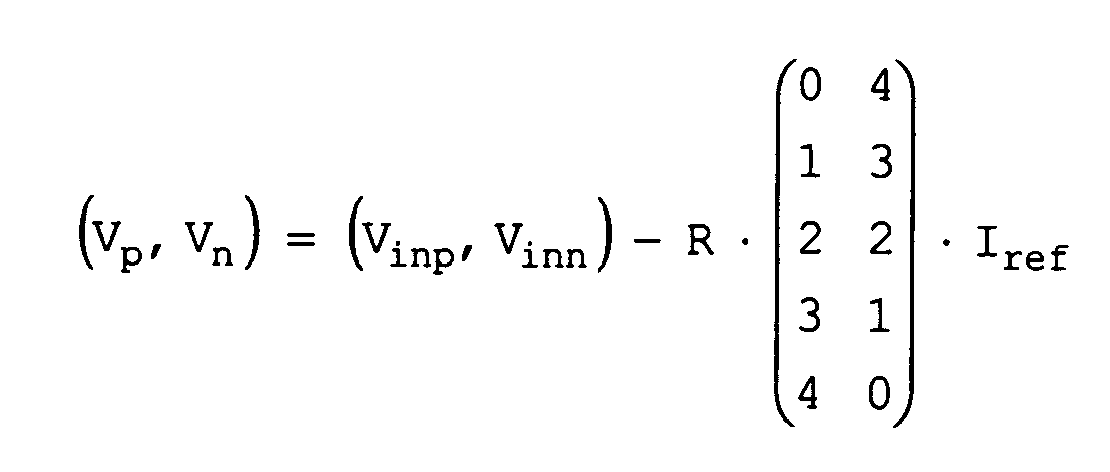
first input ports resistors - With the above matrix representation the voltages Vp and Vn of the left hand side and the right hand side can be obtained from:
- The general case as shown in Fig. 3 also represents the practical approach in that at each input port of a difference detection device a current source is located in order to provide the same capacitive input characteristic for all combinations of resistances (31-35; 41-45), current sources (71-75; 81-85) and difference detection means (131-135) .
- As for the prior art described with respect to Fig. 2, the current of the current sources which operate actually as current sinks is supplied via the input terminals Vinp and Vinn through a suitable driving circuit, such as an emitter follower. Unlike in the prior art, Iref does not strictly need to be tuned to a current magnitude that is large with respect to the input currents of the difference detection means. A difference detection means will provide information on the voltage level when the voltage at both inputs,
e.g. inputs 93 and 103, are almost equal. At this instance the input currents of both, the first and the second input terminal, are also equal, so that the voltage difference is not affected. - Careful analysis shows that the circuit of Fig. 3 requires tighter tolerances on resistor values than circuits based on resistor chains to achieve a given overall accuracy. For this reason, it may be necessary in some cases to calibrate the reference currents in order to meet accuracy requirements.
- Fig. 4 illustrates the sample circuit where the current magnitudes k · Iref are distributed in the manner that k starts from 0 incrementing up to 4 from difference detection means 131 towards difference detection means 135 for the left hand side current sources 71 to 75 in Fig. 3 and decrementing from 4 down to 0 for the right hand side sources 81 to 85 in Fig. 3. The arrangement of the
resistors positive input terminal 1 and on the other side with thepositive input port 91 to 95 of the difference detection means 131 to 135. Alsoresistors 41 to 45 are connected on one side with the negative input ports 101 to 105 and on the other side withnegative input terminal 2. The current sources with currents of 0 have been left out of the drawing. For the example in Fig. 4 differential offset voltages L·R·Iref, with L ∈ {-4, -2, 0, 2, 4} are obtained which provide a linear distribution of the differential voltages. - Fig. 5 shows an embodiment where the currents of the left hand side current sources 71 to 75 of Fig. 3 are all set to zero and the right hand side current sources 81 to 85 provide currents that correspond to the differential offset voltages of the circuit shown in Figure 4. The matrix representation of the current distribution is

in this case. - Fig. 6 shows an embodiment of the invention analog-to-digital converter with an asymmetric distribution of the current sources. As in Fig. 5 current sources with a current of 0 are left out and the corresponding matrix representation can be given as:

- The invention is not restricted to the above embodiments and can be used with different implementations. The current sources and the input stages of the differential amplifiers can be implemented in bipolar technology but also in CMOS technology. The current sources can be configured as current mirror circuits. All features described in this description and shown in the accompanying drawings can be combined.
Claims (15)
- Analog-to-digital converter comprising:a positive input terminal (1),a negative terminal (2),several difference detection means (131, 132, 133, 134, 135) detecting a voltage difference between a positive input port (91, 92, 93, 94, 95) and a negative input port (101, 102, 103, 104, 105),first resistors (31, 32, 33, 34, 35) connecting each positive input port (91, 92, 93, 94, 95) of each difference detection means (131, 132, 133, 134, 135) with the positive input terminal (1),second resistors (41, 42, 43, 44, 45) connecting each negative input port (101, 102, 103, 104, 105) of each difference detection means (131, 132, 133, 134, 135) to the negative input terminal (2),and at least one current source.
- Analog-to-digital converter according to claim 1,
wherein at least two first current sources (71, 72, 73, 74, 75) are connected to the positive input port (91, 92, 93, 94, 95) of at least two of the difference detection means (131, 132, 133, 134, 135) generating different currents (Iref, 2Iref, 3Iref, 4Iref) and/or
wherein at least two second current sources (81, 82, 83, 84, 85) are connected to the negative input port (101, 102, 103, 104, 105) of at least two of the difference detection means (131, 132, 133, 134, 135) generating different currents (4Iref, 3Iref, 2Iref, 1Iref). - Analog-to-digital converter according to claim 2,
wherein the difference of the currents of the first current sources (Iref, 2Iref, 3Iref, 4Iref) and/or of the second current sources (4Iref, 3Iref, 2Iref, 1Iref) increases or decreases linearly from one difference detection means (131, 132, 133, 134) to the next difference detection means (132, 133, 134, 135) . - Analog-to-digital converter according to claim 2,
wherein the difference of the currents of the first current sources (71, 72, 73, 74, 75) and/or of the second current sources (81, 82, 83, 84, 85) increases or decreases nonlinearly from one difference detection means (131, 132, 133, 134) to the next difference detection means (132, 133, 134, 135). - Analog-to-digital converter according to any of claims 1 to 4,
wherein the first resistors (31, 32, 33, 34, 35) have equal resistance. - Analog-to-digital converter according to any of claims 1 to 5,
wherein the second resistors (41, 42, 43, 44, 45) have equal resistance. - Analog-to-digital converter according to any of claims 1 to 6,
wherein the first resistors (31, 32, 33, 34, 35) and/or the second resistors (41, 42, 43, 44, 45) directly connect the respective input terminal (1; 2) with the respective input port (91, 92, 93, 94, 95; 101, 102, 103, 104, 105) of the difference detection means (131, 132, 133, 134, 135) in the manner of a star network. - Analog-to-digital converter according to any of claims 2 to 4,
wherein the sums of currents of the first and second current sources (71, 81; 72, 82; 73, 83; 74, 84; 75, 85) that are connected to the same difference detection means (131, 132, 133, 134, 135) are equal for each difference detection means (131, 132, 133, 134, 135). - Analog-to-digital converter according to any of claims 2 to 4 or 8,
wherein the currents (Iref, 2Iref, 3Iref, 4Iref) generated by the first and second current sources (71-75, 81-85) are integer multiples of a reference current (Iref). - Analog-to-digital converter according to claim 9,
wherein the reference currents (Iref) of the first current sources (71-75) and the reference currents of the second current sources (81-85) are identical. - Analog-to-digital converter according to any of claims 1 to 10,
wherein a first difference detection means (131) has a current source (81) only at its negative input port (101). - Analog-to-digital converter according to claim 11,
wherein a last difference detection means (135) has a current source (75) only at its positive input port (95). - Analog-to-digital converter according to claim 12,
wherein the remaining difference detection means (132-134) have current sources (72, 82; 73, 83; 74, 84) at its positive input ports (92, 93, 94) and its negative input ports (102, 103, 104). - Analog-to-digital converter according to claim 1 or 2,
wherein current sources (81, 82, 84, 85) generating a current differing from zero are connected to positive input ports only or to negative input ports (101, 102, 104, 105) of the difference detection means (131 - 135) only. - Analog-to-digital converter according to claim 1 or 2,
wherein first current sources (74, 75) generating a current differing form zero are only connected to the positive input ports (94, 95) of a first set (134, 135) of difference detection means and wherein second current sources (81, 82) generating a current differing from zero are only connected to the negative input ports (101, 102) of a second set (131, 132) of difference detection means, whereby the first set (134, 135) and the second set (131, 132) do not comprise any identical difference detection means.
Priority Applications (4)
| Application Number | Priority Date | Filing Date | Title |
|---|---|---|---|
| DE602005005823T DE602005005823T2 (en) | 2005-09-12 | 2005-09-12 | Fast analog-to-digital converter |
| EP05019801A EP1770866B1 (en) | 2005-09-12 | 2005-09-12 | High-speed analog/digital converter |
| JP2006170220A JP4727511B2 (en) | 2005-09-12 | 2006-06-20 | High-speed analog / digital converter |
| US11/470,789 US7394420B2 (en) | 2005-09-12 | 2006-09-07 | High-speed analog/digital converter |
Applications Claiming Priority (1)
| Application Number | Priority Date | Filing Date | Title |
|---|---|---|---|
| EP05019801A EP1770866B1 (en) | 2005-09-12 | 2005-09-12 | High-speed analog/digital converter |
Publications (2)
| Publication Number | Publication Date |
|---|---|
| EP1770866A1 true EP1770866A1 (en) | 2007-04-04 |
| EP1770866B1 EP1770866B1 (en) | 2008-04-02 |
Family
ID=35058860
Family Applications (1)
| Application Number | Title | Priority Date | Filing Date |
|---|---|---|---|
| EP05019801A Expired - Lifetime EP1770866B1 (en) | 2005-09-12 | 2005-09-12 | High-speed analog/digital converter |
Country Status (4)
| Country | Link |
|---|---|
| US (1) | US7394420B2 (en) |
| EP (1) | EP1770866B1 (en) |
| JP (1) | JP4727511B2 (en) |
| DE (1) | DE602005005823T2 (en) |
Families Citing this family (7)
| Publication number | Priority date | Publication date | Assignee | Title |
|---|---|---|---|---|
| SI22397A (en) * | 2006-10-11 | 2008-04-30 | Anton Pletersek | Interpolation procedure and circuit for performing such a procedure applied in high resolution encoding devices |
| DE102009002062B4 (en) * | 2009-03-31 | 2013-08-22 | Ihp Gmbh - Innovations For High Performance Microelectronics / Leibniz-Institut Für Innovative Mikroelektronik | Analog-to-digital converter with broadband input network |
| US7936298B2 (en) * | 2009-09-18 | 2011-05-03 | Mediatek Singapore Pte. Ltd. | Integrated circuit and electronic device comprising threshold generation circuitry and method therefor |
| RU2536377C1 (en) * | 2013-04-26 | 2014-12-20 | Федеральное государственное бюджетное образовательное учреждение высшего профессионального образования "Южно-Российский государственный университет экономики и сервиса" (ФГБОУ ВПО "ЮРГУЭС") | Ultra-high-speed parallel analogue-to-digital converter with differential input |
| RU2523960C1 (en) * | 2013-04-30 | 2014-07-27 | Федеральное государственное бюджетное образовательное учреждение высшего профессионального образования "Южно-Российский государственный университет экономики и сервиса" (ФГБОУ ВПО "ЮРГУЭС") | Ultra-high-speed parallel analogue-to-digital converter with differential input |
| RU2518997C1 (en) * | 2013-04-30 | 2014-06-10 | Федеральное государственное бюджетное образовательное учреждение высшего профессионального образования "Южно-Российский государственный университет экономики и сервиса" (ФГБОУ ВПО "ЮРГУЭС") | Ultra-high-speed parallel analogue-to-digital converter with differential input |
| DE102015212842A1 (en) * | 2015-07-09 | 2017-01-12 | Forschungszentrum Jülich GmbH | Voltage amplifier for a programmable voltage range |
Citations (10)
| Publication number | Priority date | Publication date | Assignee | Title |
|---|---|---|---|---|
| US3984832A (en) * | 1975-06-06 | 1976-10-05 | Motorola, Inc. | Series current analog to digital converter |
| US5396131A (en) * | 1992-03-05 | 1995-03-07 | Mitsubishi Denki Kabushiki Kaisha | Differential amplifier, comparator and high-speed A/D converter using the same |
| US5598161A (en) * | 1992-12-18 | 1997-01-28 | Sony Corporation | Analog-to-digital converter having reduced circuit area |
| US5600275A (en) * | 1994-04-29 | 1997-02-04 | Analog Devices, Inc. | Low-voltage CMOS comparator with offset cancellation |
| US5736952A (en) * | 1996-10-09 | 1998-04-07 | International Business Machines Corporation | Current boost for differential flash analog to digital converter driver |
| US6437724B1 (en) * | 1999-11-05 | 2002-08-20 | Texas Instruments Incorporated | Fully differential flash A/D converter |
| US6445221B1 (en) * | 2000-03-10 | 2002-09-03 | International Business Machines Corporation | Input driver for a differential folder employing a static reference ladder |
| WO2002078191A2 (en) * | 2001-03-23 | 2002-10-03 | Walter Snoeijs | Current folding cell and circuit comprising at least one folding cell |
| WO2003088498A1 (en) * | 2002-04-05 | 2003-10-23 | Ess Technology, Inc. | Differential input flash analog to digital converter |
| US20050030216A1 (en) * | 2003-08-06 | 2005-02-10 | Linder Lloyd F. | Resistive ladder, summing node circuit, and trimming method for a subranging analog to digital converter |
Family Cites Families (11)
| Publication number | Priority date | Publication date | Assignee | Title |
|---|---|---|---|---|
| FR2268399B1 (en) * | 1974-04-22 | 1976-10-08 | Adersa | |
| FR2427012A1 (en) * | 1978-05-24 | 1979-12-21 | Labo Electronique Physique | BINARY ANALOGUE-DIGITAL CONVERTER |
| DE3686705T2 (en) * | 1985-12-16 | 1993-04-01 | Philips Nv | CIRCUIT FOR INTERPOLATION BETWEEN COMPLEMENTAL VOLTAGES. |
| DE4004546A1 (en) * | 1990-02-14 | 1991-08-22 | Siemens Ag | DIFFERENTIAL ANALOG-DIGITAL CONVERTER |
| US5175550A (en) * | 1990-06-19 | 1992-12-29 | Analog Devices, Inc. | Repetitive cell matching technique for integrated circuits |
| US5157397A (en) * | 1991-01-28 | 1992-10-20 | Trw Inc. | Quantizer and related method for improving linearity |
| US5231399A (en) * | 1991-09-27 | 1993-07-27 | Trw Inc. | Differential quantizer reference resistor ladder for use with an analog-to-digital converter |
| US5376937A (en) * | 1993-02-22 | 1994-12-27 | The Regents Of The University Of California | Folding circuit |
| US5589831A (en) * | 1995-01-30 | 1996-12-31 | Samsung Semiconductor, Inc. | Fully differential flash ADC based on the voltage follower amplifier structure |
| FR2863120B1 (en) * | 2003-12-02 | 2006-02-17 | Atmel Grenoble Sa | FAST ANALOG-TO-DIGITAL CONVERTER |
| US6847320B1 (en) * | 2004-02-13 | 2005-01-25 | National Semiconductor Corporation | ADC linearity improvement |
-
2005
- 2005-09-12 EP EP05019801A patent/EP1770866B1/en not_active Expired - Lifetime
- 2005-09-12 DE DE602005005823T patent/DE602005005823T2/en not_active Expired - Lifetime
-
2006
- 2006-06-20 JP JP2006170220A patent/JP4727511B2/en not_active Expired - Lifetime
- 2006-09-07 US US11/470,789 patent/US7394420B2/en active Active
Patent Citations (10)
| Publication number | Priority date | Publication date | Assignee | Title |
|---|---|---|---|---|
| US3984832A (en) * | 1975-06-06 | 1976-10-05 | Motorola, Inc. | Series current analog to digital converter |
| US5396131A (en) * | 1992-03-05 | 1995-03-07 | Mitsubishi Denki Kabushiki Kaisha | Differential amplifier, comparator and high-speed A/D converter using the same |
| US5598161A (en) * | 1992-12-18 | 1997-01-28 | Sony Corporation | Analog-to-digital converter having reduced circuit area |
| US5600275A (en) * | 1994-04-29 | 1997-02-04 | Analog Devices, Inc. | Low-voltage CMOS comparator with offset cancellation |
| US5736952A (en) * | 1996-10-09 | 1998-04-07 | International Business Machines Corporation | Current boost for differential flash analog to digital converter driver |
| US6437724B1 (en) * | 1999-11-05 | 2002-08-20 | Texas Instruments Incorporated | Fully differential flash A/D converter |
| US6445221B1 (en) * | 2000-03-10 | 2002-09-03 | International Business Machines Corporation | Input driver for a differential folder employing a static reference ladder |
| WO2002078191A2 (en) * | 2001-03-23 | 2002-10-03 | Walter Snoeijs | Current folding cell and circuit comprising at least one folding cell |
| WO2003088498A1 (en) * | 2002-04-05 | 2003-10-23 | Ess Technology, Inc. | Differential input flash analog to digital converter |
| US20050030216A1 (en) * | 2003-08-06 | 2005-02-10 | Linder Lloyd F. | Resistive ladder, summing node circuit, and trimming method for a subranging analog to digital converter |
Non-Patent Citations (3)
| Title |
|---|
| "DIFFERENTIAL HIGH-SPEED ANALOG TO DIGITAL CONVERTER", IBM TECHNICAL DISCLOSURE BULLETIN, IBM CORP. NEW YORK, US, vol. 38, no. 1, January 1995 (1995-01-01), pages 425 - 427, XP000498822, ISSN: 0018-8689 * |
| LEE J. ET AL: "A 5-b 10-GSample/s A/D converter for 10-Gb/s Optical Receivers", IEEE JOURNAL OF SOLID-STATE CIRCUITS, vol. 39, no. 10, 10 October 2004 (2004-10-10), pages 1671 - 1679, XP002350895 * |
| SCHOLTENS P C S ET AL: "A 6-B 1.6-GSAMPLE/S FLASH ADC IN 0.18-MUM CMOS USING AVERAGING TERMINATION", IEEE JOURNAL OF SOLID-STATE CIRCUITS, IEEE INC. NEW YORK, US, vol. 37, no. 12, December 2002 (2002-12-01), pages 1599 - 1609, XP001222714, ISSN: 0018-9200 * |
Also Published As
| Publication number | Publication date |
|---|---|
| US20070057832A1 (en) | 2007-03-15 |
| US7394420B2 (en) | 2008-07-01 |
| DE602005005823T2 (en) | 2009-05-07 |
| JP2007082184A (en) | 2007-03-29 |
| EP1770866B1 (en) | 2008-04-02 |
| JP4727511B2 (en) | 2011-07-20 |
| DE602005005823D1 (en) | 2008-05-15 |
Similar Documents
| Publication | Publication Date | Title |
|---|---|---|
| EP1561339B1 (en) | Read-out circuit for infrared detectors | |
| CN102217192B (en) | Variable gain amplifier | |
| CN102771052A (en) | Source follower input buffer | |
| US6700417B2 (en) | Sampling and hold circuit | |
| US6812787B2 (en) | Reference voltage generating circuit and voltage amplifier using the same | |
| US7532069B2 (en) | Differential amplifying circuit | |
| US9160293B2 (en) | Analog amplifiers and comparators | |
| EP1770866B1 (en) | High-speed analog/digital converter | |
| EP1315290B1 (en) | Pseudo-differential amplifier and analog-to-digital converter using the same | |
| US8907831B1 (en) | High-resolution digital to analog converter | |
| US7714264B2 (en) | Semiconductor integrated circuit device | |
| US20220173744A1 (en) | Low noise hybrid comparator | |
| CN116015256B (en) | Comparator with offset cancellation | |
| CN101512906A (en) | Folding circuits and analog-to-digital converters | |
| US6172636B1 (en) | Linearizing structures and methods for adjustable-gain folding amplifiers | |
| US6614379B2 (en) | Precise differential voltage interpolation analog-to-digital converter having double interpolation using nonlinear resistors | |
| EP2995004B1 (en) | Differential sampling circuit with harmonic cancellation | |
| KR20080077200A (en) | How Switchable Folding Circuits, Analog-to-Digital Converters, and Switchable Folding Circuits Work | |
| US9837997B2 (en) | Comparison circuit and sensor device | |
| JP5238856B2 (en) | Differential amplifier circuit and A / D converter | |
| US6492930B2 (en) | Reduced propagation delay current mode cascaded analog-to-digital converter and threshold bit cell therefor | |
| US7088274B2 (en) | Difference amplifier for digital-to-analog converter | |
| JP7361062B2 (en) | amplifier circuit | |
| US6091353A (en) | Bias circuit for flash analog to digital converter circuits | |
| JP3830914B2 (en) | Monolithic chip integrated circuit including repeatable cells for A / D converters |
Legal Events
| Date | Code | Title | Description |
|---|---|---|---|
| PUAI | Public reference made under article 153(3) epc to a published international application that has entered the european phase |
Free format text: ORIGINAL CODE: 0009012 |
|
| 17P | Request for examination filed |
Effective date: 20060309 |
|
| AK | Designated contracting states |
Kind code of ref document: A1 Designated state(s): AT BE BG CH CY CZ DE DK EE ES FI FR GB GR HU IE IS IT LI LT LU LV MC NL PL PT RO SE SI SK TR |
|
| AX | Request for extension of the european patent |
Extension state: AL BA HR MK YU |
|
| GRAP | Despatch of communication of intention to grant a patent |
Free format text: ORIGINAL CODE: EPIDOSNIGR1 |
|
| AKX | Designation fees paid |
Designated state(s): DE FR GB |
|
| GRAS | Grant fee paid |
Free format text: ORIGINAL CODE: EPIDOSNIGR3 |
|
| GRAA | (expected) grant |
Free format text: ORIGINAL CODE: 0009210 |
|
| AK | Designated contracting states |
Kind code of ref document: B1 Designated state(s): DE FR GB |
|
| REG | Reference to a national code |
Ref country code: GB Ref legal event code: FG4D |
|
| REF | Corresponds to: |
Ref document number: 602005005823 Country of ref document: DE Date of ref document: 20080515 Kind code of ref document: P |
|
| ET | Fr: translation filed | ||
| PLBE | No opposition filed within time limit |
Free format text: ORIGINAL CODE: 0009261 |
|
| STAA | Information on the status of an ep patent application or granted ep patent |
Free format text: STATUS: NO OPPOSITION FILED WITHIN TIME LIMIT |
|
| 26N | No opposition filed |
Effective date: 20090106 |
|
| REG | Reference to a national code |
Ref country code: FR Ref legal event code: PLFP Year of fee payment: 11 |
|
| REG | Reference to a national code |
Ref country code: FR Ref legal event code: PLFP Year of fee payment: 12 |
|
| REG | Reference to a national code |
Ref country code: FR Ref legal event code: PLFP Year of fee payment: 13 |
|
| REG | Reference to a national code |
Ref country code: FR Ref legal event code: PLFP Year of fee payment: 14 |
|
| P01 | Opt-out of the competence of the unified patent court (upc) registered |
Effective date: 20230525 |
|
| PGFP | Annual fee paid to national office [announced via postgrant information from national office to epo] |
Ref country code: DE Payment date: 20240919 Year of fee payment: 20 |
|
| PGFP | Annual fee paid to national office [announced via postgrant information from national office to epo] |
Ref country code: GB Payment date: 20240923 Year of fee payment: 20 |
|
| PGFP | Annual fee paid to national office [announced via postgrant information from national office to epo] |
Ref country code: FR Payment date: 20240924 Year of fee payment: 20 |
|
| REG | Reference to a national code |
Ref country code: DE Ref legal event code: R071 Ref document number: 602005005823 Country of ref document: DE |
|
| REG | Reference to a national code |
Ref country code: GB Ref legal event code: PE20 Expiry date: 20250911 |