EP1768195A2 - Light emitting diode and method for manufacturing the same - Google Patents
Light emitting diode and method for manufacturing the same Download PDFInfo
- Publication number
- EP1768195A2 EP1768195A2 EP06254940A EP06254940A EP1768195A2 EP 1768195 A2 EP1768195 A2 EP 1768195A2 EP 06254940 A EP06254940 A EP 06254940A EP 06254940 A EP06254940 A EP 06254940A EP 1768195 A2 EP1768195 A2 EP 1768195A2
- Authority
- EP
- European Patent Office
- Prior art keywords
- light emitting
- phosphor
- emitting element
- concentration
- light
- Prior art date
- Legal status (The legal status is an assumption and is not a legal conclusion. Google has not performed a legal analysis and makes no representation as to the accuracy of the status listed.)
- Withdrawn
Links
Images







Classifications
-
- H—ELECTRICITY
- H10—SEMICONDUCTOR DEVICES; ELECTRIC SOLID-STATE DEVICES NOT OTHERWISE PROVIDED FOR
- H10H—INORGANIC LIGHT-EMITTING SEMICONDUCTOR DEVICES HAVING POTENTIAL BARRIERS
- H10H20/00—Individual inorganic light-emitting semiconductor devices having potential barriers, e.g. light-emitting diodes [LED]
- H10H20/80—Constructional details
- H10H20/85—Packages
- H10H20/851—Wavelength conversion means
- H10H20/8516—Wavelength conversion means having a non-uniform spatial arrangement or non-uniform concentration, e.g. patterned wavelength conversion layer or wavelength conversion layer with a concentration gradient
-
- H—ELECTRICITY
- H10—SEMICONDUCTOR DEVICES; ELECTRIC SOLID-STATE DEVICES NOT OTHERWISE PROVIDED FOR
- H10H—INORGANIC LIGHT-EMITTING SEMICONDUCTOR DEVICES HAVING POTENTIAL BARRIERS
- H10H20/00—Individual inorganic light-emitting semiconductor devices having potential barriers, e.g. light-emitting diodes [LED]
- H10H20/80—Constructional details
- H10H20/85—Packages
- H10H20/852—Encapsulations
- H10H20/853—Encapsulations characterised by their shape
-
- H—ELECTRICITY
- H10—SEMICONDUCTOR DEVICES; ELECTRIC SOLID-STATE DEVICES NOT OTHERWISE PROVIDED FOR
- H10H—INORGANIC LIGHT-EMITTING SEMICONDUCTOR DEVICES HAVING POTENTIAL BARRIERS
- H10H20/00—Individual inorganic light-emitting semiconductor devices having potential barriers, e.g. light-emitting diodes [LED]
- H10H20/80—Constructional details
- H10H20/84—Coatings, e.g. passivation layers or antireflective coatings
-
- H—ELECTRICITY
- H10—SEMICONDUCTOR DEVICES; ELECTRIC SOLID-STATE DEVICES NOT OTHERWISE PROVIDED FOR
- H10W—GENERIC PACKAGES, INTERCONNECTIONS, CONNECTORS OR OTHER CONSTRUCTIONAL DETAILS OF DEVICES COVERED BY CLASS H10
- H10W72/00—Interconnections or connectors in packages
- H10W72/50—Bond wires
- H10W72/551—Materials of bond wires
- H10W72/552—Materials of bond wires comprising metals or metalloids, e.g. silver
- H10W72/5522—Materials of bond wires comprising metals or metalloids, e.g. silver comprising gold [Au]
-
- H—ELECTRICITY
- H10—SEMICONDUCTOR DEVICES; ELECTRIC SOLID-STATE DEVICES NOT OTHERWISE PROVIDED FOR
- H10W—GENERIC PACKAGES, INTERCONNECTIONS, CONNECTORS OR OTHER CONSTRUCTIONAL DETAILS OF DEVICES COVERED BY CLASS H10
- H10W72/00—Interconnections or connectors in packages
- H10W72/851—Dispositions of multiple connectors or interconnections
- H10W72/874—On different surfaces
- H10W72/884—Die-attach connectors and bond wires
Definitions
- the present invention relates to a light emitting device which is provided with a light emitting element and a phosphor, and which is configured to emit light, and a method for manufacturing the light emitting device.
- a known conventional light emitting device which is provided with a light emitting element and a phosphor, is configured in the following manner, for example.
- a lead frame which is provided with a concave section, is used to mount a light emitting diode (LED), which is the light emitting element, on a bottom surface of the concave section of the lead frame.
- the phosphor is mixed with a transparent resin, and the concave section is fully filled with this phosphor-containing resin so that the resin covers the LED.
- the phosphor is designed to absorb light emitted from the LED, and is designed to convert the light into light having a different wavelength.
- a blue LED is used as the LED and the phosphor configured to convert wavelength of the light for the blue LED into that for yellow is used, for example.
- a near ultraviolet LED is used as the LED and the phosphor configured to convert wavelength of the light for the near ultraviolet LED into those for three colors of red, green, and blue is used.
- a light emitting device enables white light to be emitted on a light emission observation surface by mixing the colors emitted from the phosphor.
- a light emitting device 800 configured in the following manner will be considered.
- a light emitting element 80 is mounted in the device, and phosphor-containing transparent resin 81 fills around the device while contacting and covering the device.
- the light emitting element 80 has a structure in which the light intensity is the highest in a direction directly above the blue LED or the near ultraviolet LED.
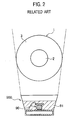
- an overhead section 2 of the light emitting element 80 looks blue or violet due to the blue light or the ultraviolet, and a surrounding section 3 looks white. Accordingly, this device causes color shading.
- the light intensity is the highest in a lateral direction and an obliquely downward direction depending on a shape of a light emitting element 90.
- an overhead section 2 of the light emitting element 90 looks white, and a surrounding section 3 exhibits a color in a blue to ultraviolet zone. Accordingly, this device causes color shading.
- Patent Document 1 Japanese Patent Publication No. 2004 - 111882
- Patent Document 2 Japanese Patent Publication No. 2004 - 349647
- the light emitting device disclosed in Patent Document 1 has a following configuration. After the light emitting element is mounted on the concave section of the lead frame, first phosphor-containing transparent resin having a low phosphor concentration is filled up to a position of an upper surface of the light emitting element. Second phosphor-containing transparent resin having a high phosphor concentration is disposed on the first phosphor-containing resin.
- a phosphor unit is disposed on a plane of an optical member located inside the light emitting device, the plane facing the light emitting element. In addition, in-plane intensity distribution of the phosphor concentration is provided within the plane. Thereby, color shading is reduced.
- An object of the present invention is to provide a light emitting device with which uniform light emission can be obtained on a light emission observation surface, and to provide a method for manufacturing the light emitting device.
- a first aspect of the present invention inheres in a light emitting device which includes a base, a light emitting element, a phosphor-containing transparent resin section, and a high-concentration phosphor-containing resin layer.
- the light emitting element is disposed on an upper surface of the base so that the light intensity of the light emitting element is higher in a direction perpendicular to the upper surface of the base than in a direction horizontal to the upper surface of the base.
- the phosphor-containing transparent resin section is provided above the light emitting element while covering an area wider than an upper surface of the light emitting element, and contains the phosphor to which the light emitted from the light emitting element is absorbed, and which emits light having a wavelength different from a wavelength of the absorbed light.
- the high-concentration phosphor-containing resin layer is formed on an upper surface of the light emitting element, and has a phosphor concentration higher than a phosphor concentration of the phosphor-containing transparent resin section.
- light emitted in the perpendicular direction from the light emitting element may be projected to the outside through the high-concentration phosphor-containing resin layer and through the phosphor-containing transparent resin section, and in which light emitted in the parallel direction from the light emitting element may be projected to the outside through the phosphor-containing transparent resin section.
- the phosphor-containing transparent resin section may have phosphor concentration in a range of 10 to 15 weight percent
- the high-concentration phosphor-containing resin layer may have phosphor concentration in a range of 20 to 25 weight percent
- a second aspect of the present invention inheres in a light emitting device which includes the base, the light emitting element, the phosphor-containing transparent resin, and a low concentration phosphor-containing resin layer.
- the light emitting element is disposed on the upper surface of the base so that the light intensity of the light emitting element is higher in a direction perpendicular to the upper surface of the base than in a direction horizontal to the upper surface of the base.
- the phosphor-containing transparent resin section is provided above the light emitting element while covering an area wider than an upper surface of the light emitting element, and contains the phosphor, to which the light emitted from the light emitting element is absorbed, and which emits light having a wavelength different from that of the absorbed light
- the low-concentration phosphor-containing resin layer is formed on the upper surface of the light emitting element, and has a phosphor concentration lower than a phosphor concentration of the phosphor-containing transparent resin section.
- light emitted in the perpendicular direction from the light emitting element may be projected to the outside through the low-concentration phosphor-containing resin layer, and in which light emitted in the parallel direction from the light emitting element may be projected to the outside through the phosphor-containing transparent resin section.
- the phosphor-containing transparent resin section may have phosphor concentration in a range of 20 to 25 weight percent, and the low-concentration phosphor-containing resin layer may have phosphor concentration in a range of 10 to 15 weight percent.
- the light emitting element may emit any one of blue light and ultraviolet light.
- a third aspect of the present invention inheres in a method for manufacturing a light emitting device, which includes: forming, on a surface of the light emitting element, a phosphor-containing resin layer containing a phosphor which absorbs light emitted from the light emitting element, and which emits light having a wavelength different from a wavelength of the absorbed light, the light emitting element being disposed on a surface of the substrate and being provided with a light emitting layer, the surface of the light emitting element facing the surface of the substrate; placing the surface of the phosphor-containing resin layer up, and disposing the light emitting element onto an upper surface of a base so that light intensity in a direction perpendicular to the upper surface of the base is higher than that in a direction parallel to the upper surface of the base; and forming a phosphor-containing transparent resin section, which has a phosphor concentration lower than a phosphor concentration of the phosphor-containing resin layer, above the light emitting element while covering an area wider than the surface of the
- a fourth aspect of the present invention inheres in a method for manufacturing a light emitting device, which includes: forming, on a surface of the light emitting element, a phosphor-containing resin layer containing a phosphor which absorbs light emitted from the light emitting element, and which emits light having a wavelength different from a wavelength of the absorbed light, the light emitting element being disposed on a surface of the substrate and being provided with a light emitting layer, the surface of the light emitting element facing the surface of the substrate; placing the surface of the phosphor-containing resin layer up, and disposing the light emitting element onto the upper surface of the base so that light intensity in a direction parallel to the upper surface of the base is higher than that in a direction perpendicular to the upper surface of the base; and forming a phosphor-containing transparent resin section, which has a phosphor concentration higher than a phosphor concentration of the phosphor-containing resin layer with surroundings of the light emitting element covered therewith.
- the phosphor-containing transparent resin section may be formed without covering an upper part of the phosphor-containing resin layer therewith.
- a light emitting device which is configured in the following manner, and a manufacturing method thereof can be provided.
- a light emitting element is disposed on the upper surface of the base so that light intensity in a direction perpendicular to the upper surface of the base is higher than that in a direction horizontal to the upper surface of the base.
- a phosphor-containing transparent resin section containing a phosphor is provided above the light emitting element while covering an area wider than an upper surface of the light emitting element, absorbs light emitted from the light emitting element, and emits light having a wavelength different from that of the absorbed light.
- a high-concentration phosphor-containing resin layer has a phosphor concentration higher than that of the phosphor-containing transparent resin section.
- phosphor-containing transparent resin which has a conventional concentration
- phosphor-containing transparent resin which has a higher phosphor concentration
- phosphor-containing transparent resin which has a higher phosphor concentration
- the high-concentration phosphor-containing resin layer on the upper surface of the light emitting element is adapted as the high-concentration phosphor-containing resin layer on the upper surface of the light emitting element.
- wavelength of the light which is radiated from the light emitting element toward the upper surface, can be converted effectively by use of the transparent resin layer having the higher phosphor concentration.
- it is made possible to radiate light which has the wavelength substantially equivalent to the wavelength converted by use of the low-concentration phosphor-containing transparent resin section around the light emitting element. Accordingly, it is made possible to provide the light emitting device, which has fine in-plane uniformity, and in which color shading of emitted light is reduced.
- a light emitting device which is configured in the following manner, and a manufacturing method thereof can be provided.
- a light emitting element is disposed on the upper surface of the base so that light intensity in a direction horizontal to the upper surface of the base is higher than that in a direction perpendicular to the upper surface of the base.
- a phosphor-containing transparent resin section containing a phosphor is provided on the upper surface of the light emitting element while covering surroundings of the light emitting element, absorbs light emitted from the light emitting element, and emits light having a wavelength different from that of the absorbed light
- a low-concentration phosphor-containing resin layer has a phosphor concentration lower than that of the phosphor-containing transparent resin section.
- phosphor-containing transparent resin which has a conventional concentration
- resin which has a phosphor concentration higher than that of the above conventional concentration
- the phosphor-containing transparent resin section covering the surroundings of the light emitting element.
- any one of the high-concentration phosphor-containing resin layer and the low-concentration phosphor-containing resin layer are formed on the upper surface of the light emitting element.
- the phosphor-containing transparent resin section is formed while covering either the upper surface, or the surroundings, of the light emitting element. Hence, positional relations are intact respectively between the light emitting element and the high-concentration phosphor-containing resin layer and between the light emitting element and the low-concentration phosphor-containing resin layer.
- the present invention can provide a light emitting device with reduced color shading at a high yield.
- FIG. 3 shows a light emitting device 100 according to a first embodiment of the present invention
- FIGs. 7A and 7B each shows a light emitting diode (LED) light emitting element 10 to be mounted thereon.
- the LED light emitting element 10 has a configuration in which a crystal growth layer 102 is formed on a surface of a sapphire crystal substrate 101, and in which a negative (n) electrode 13 and a positive (p) electrode 14 are respectively formed in appropriate positions.
- the crystal growth layer 102 is a gallium nitride based material, and includes a light emitting layer.
- a high-concentration phosphor-containing resin layer 12 is formed on an upper surface of the crystal growth layer 102.
- the high-concentration phosphor-containing resin layer 12 is made of transparent resin containing a high concentration of a phosphor (hereinafter referred to as "first phosphor-containing resin").
- the light emitting element 10 is mounted, in the form of a junction-up type, on an upper surface of a concave section of a base 15 in which a side, where the crystal growth layer 102 is formed, is placed up.
- the LED light emitting element 10 is disposed such that light intensity in a direction perpendicular to the upper surface of the base 15 is higher than that in a direction parallel to the upper surface of the base 15.
- the light emitting device 100 has a following configuration.
- the light emitting element 10 is disposed on the upper surface of the concave section of the base 15.
- wires 16 and 17 are respectively connected to the n electrode 13 and the p electrode 14, and a feed pattern (not shown) is connected to each of the wires 16 and 17.
- a low-concentration phosphor-containing resin section 18, which covers the entire light emitting element 10, is formed by filling the concave section of the base 15 with transparent resin containing a concentration of the phosphor lower than that of the first phosphor-containing resin (hereinafter referred to as "second phosphor-containing resin").
- the phosphor concentration of the second phosphor-containing resin having a lower phosphor concentration is substantially equivalent to that of phosphor-containing transparent resin which has been conventionally applied to a LED light emitting element of a similar type.
- the concentration is set in a range of 10 to 15 w%.
- the phosphor concentration of the first phosphor-containing resin, which has a higher concentration is adjusted to an appropriate concentration for achieving in-plane uniformity of emitted colors on a light emission observation surface 1 of the light emitting device 100, e.g., in a range of 20 to 25 w%.
- semiconductor crystal growth layer 102 of the gallium nitride based material is formed, as the LED light emitting element 10, on the crystal substrate 101 made of a sapphire substrate.
- a crystal growth wafer 110 for blue or near ultraviolet LEDs is fabricated.
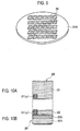
- a fabrication process, such as a process of fabricating an electrode, is performed to form LED structures. After the fabrication process, the respective LED structures are formed on the wafer 110, as shown in FIG 5.
- transparent resin is coated on a surface facing a surface of the crystal growth wafer 110, the surface being that of the semiconductor crystal growth layer 102 in the first embodiment.
- the above transparent resin is the first phosphor-containing resin in the first embodiment, and contains a higher concentration of a phosphor than that of a usual case.
- the high-concentration phosphor-containing resin layer 12 is formed by thermosetting or photocuring the above transparent resin.
- the light emitting element 10 adopted in the first embodiment is a light emitting diode of a junction-up mounting type, and uses the insulating substrate 101 made of the sapphire substrate. Accordingly, as shown in FIGs. 7A and 7B, both of the n electrode 13 and the p electrode 14 are formed on the surface where the high-concentration phosphor-containing resin layer 12 is formed.
- the high-concentration phosphor-containing resin layer 12 is formed so that the high-concentration phosphor-containing resin layer 12 is not formed in the regions corresponding to the respective electrodes 13 and 14.
- the high-concentration phosphor-containing resin layer 12 is formed by coating the uncured first phosphor-containing resin by use of the method such as dispensing, screen printing or dot printing, and then by thermosetting or photocuring the resin.
- the crystal growth wafer 110 is cut out into desired dimensions by scribing, dicing or the like, and is thereby split into individual chips respectively constituting the light emitting elements 10.
- Each side of an L chip has a length of 0.35 mm, for example.
- each of the light emitting elements 10, which is split into a chip, is mounted and fixed, in the form of the junction-up type, on the surface of the concave section of the base 15 with a conductive adhesive such as Ag paste while placing the crystal growth layer 102 up.
- a conductive adhesive such as Ag paste
- electric conductivity is achieved with the gold wires 16 and 17.
- the concave section of the base 15 is filled with the second phosphor containing resin by dispensing, and is treated with thermosetting.
- the low-concentration phosphor-containing resin section 18 is formed.
- the second phosphor-containing resin has a phosphor concentration of 10 to 15 w%, which is lower than that of the high-concentration phosphor-containing resin layer 12 formed on the surface of the semiconductor crystal growth layer 102. Accordingly, the light emitting device 100 is obtained.
- the light which has the high light intensity, and which is emitted from the light emitting element 10 in the direction perpendicular to the upper surface of the base 15, is converted effectively into light having a different wavelength by the phosphor in the high-concentration phosphor-containing resin layer 12. Consequently, as compared to the conventional case, in which the central section 2 of the light emission observation surface 1 is heavily tinted by a blue to a near ultraviolet color, and in which the peripheral section 3 exhibits a white color, as shown in FIG 1, the light emitting device 100 of the first embodiment causes the white color in the central section 2 as well. In this way, it is made possible to reduce color shading of the emitted light between the central section 2 and the peripheral section 3, and thereby to improve the in-plane uniformity.
- the high-concentration phosphor-containing resin layer 12 is formed directly on the surface of the crystal growth layer 102. Accordingly, a positional relation is intact between the high-concentration phosphor-containing resin layer 12 and the light emitting element 10. Furthermore, the low-concentration phosphor-containing resin section 18 is formed while covering the light emitting element 10 on which the high-concentration phosphor-containing resin layer 12 is formed. Thereby, positional relations are also intact respectively between the low-concentration phosphor-containing resin section 18 and the high-concentration phosphor-containing resin layer 12 and between the low-concentration phosphor-containing resin section 18 and the light emitting element 10. It is made possible to obtain the light emitting device with which the color shading of the emitted light is reduced, and with which the in-plane uniformity of the emitted colors is improved, at a high yield.
- the structure of the light emitting device 100 of the first embodiment makes it possible to reduce color shading on the light emission observation surface, and to improve the in-plane uniformity irrespective of the shape of the light emitting device such as a round type or a surface mount type.
- FIG. 8 shows a light emitting device 200 according to a second embodiment of the present invention
- FIGs. 10A and 10B each show a LED light emitting element 20 to be mounted thereon.
- the LED light emitting element 20 according to the second embodiment is a light emitting element configured to have light intensity in the perpendicular direction higher than that in the parallel direction.
- the LED light emitting element 20 includes a crystal growth layer 202 of a gallium nitride based material, a p electrode 21, and an n electrode.
- the crystal growth layer 202 includes a light emitting layer formed on a surface of a conductive substrate 201 such as a GaN substrate.
- the p electrode 21 is formed in an appropriate position on a surface of the crystal growth layer 202.
- the n electrode is formed in an appropriate position on a back surface of the conductive substrate 201.
- the light emitting element 20 is mounted, in the form of a junction-up type, on an upper surface of a base 25, in which a side where the crystal growth layer 202 is formed is placed up. Hence, in the second embodiment, the light emitting element 20 is disposed such that light intensity in a direction perpendicular to the upper surface of the base 25 is higher than that in a direction parallel to the upper surface of the base 25.
- the light emitting device 200 has a following configuration.
- the light emitting element 20 is disposed on an upper surface of the concave section of the base 25.
- a wire 23 is connected to the p electrode 21 and to a feed pattern (not shown) by bonding.
- a low-concentration phosphor-containing resin section 24, which covers the entire light emitting element 20, is formed by filling the concave section of the base 25 with the second phosphor-containing resin having the concentration of the phosphor lower than that of the first phosphor-containing resin.
- the phosphor concentration of the second phosphor-containing resin, which has the lower phosphor concentration, and the phosphor concentration of the first phosphor-containing resin, which has the high phosphor concentration are set similar to those in the first embodiment
- the p electrode 21 is formed on a surface where the high-concentration phosphor-containing resin layer 22 made of the first phosphor-containing resin is formed.
- the high-concentration phosphor-containing resin layer 22 in which the phosphor concentration thereof is adjusted to the high concentration from 20 to 25 w%, on the surface of the crystal growth layer 202, the high-concentration phosphor-containing resin layer 22 is formed so that the high-concentration phosphor-containing resin layer 22 is not formed in the region corresponding to the p electrode 21.
- the high concentration phosphor-containing resin layer 22 is formed by coating the first phosphor-containing resin by use of the method such as dispensing, screen printing or dot printing, and then by thermosetting or photocuring the resin. Thereafter, the crystal growth wafer 210 is cut out into desired dimensions, such as 0.35 mm on a side, by scribing, dicing or the like, and is thereby split into individual chips respectively constituting the light emitting elements 20.
- each of the light emitting element 20, which is split into a chip, is mounted and fixed, in the form of the junction-up type, on the concave section of the base 25 with a conductive adhesive such as Ag paste while placing the crystal growth layer 202 up.
- a conductive adhesive such as Ag paste
- the concave section of the base 25 is filled with the second phosphor containing resin by dispensing, and is treated with thermosetting.
- the low-concentration phosphor containing resin section 24 is formed.
- the second phosphor-containing resin contains a phosphor concentration lower than that of the high-concentration phosphor-containing resin layer 22, which is formed on the surface of the semiconductor crystal growth layer 202. Accordingly, the light emitting device 200 is obtained.
- the light emitting device 200 thus manufactured When the light emitting device 200 thus manufactured is energized to emit light, color shading of the emitted light between the central section 2 and the peripheral section 3 is reduced on the light emission observation surface 1, shown in FIG 8, and the in-plane uniformity is improved as in the case of the first embodiment.
- the high-concentration phosphor-containing resin layer 22 is formed directly on the surface of the crystal growth layer 202. Accordingly, a positional relation is intact between the high-concentration phosphor-containing resin layer 22 and the light emitting element 20.
- the low-concentration phosphor-containing resin section 24 is formed while covering the light emitting element 20 on which the high-concentration phosphor-containing resin layer 22 is formed.
- the light emitting device 200 of the second embodiment also makes it possible to reduce color shading on the light emission observation surface, and to improve the in-plane uniformity irrespective of the shape of the light emitting device such as the round type or the surface mount type.
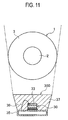
- FIG 11 shows a light emitting device 300 according to a third embodiment of the present invention
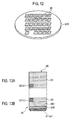
- FIGs. 13A and 13B each show a light emitting element 30 to be mounted thereon.
- the light emitting element 30 is mounted and disposed in the form of a junction-down type.
- the LED light emitting element 30 includes a crystal growth layer 302 of a gallium nitride based material, a p electrode 31, and an n electrode 32.
- the crystal growth layer 302 includes a light emitting layer formed on a surface of a conductive substrate 301 such as a GaN substrate.
- the p electrode 31 is formed in an appropriate position on a surface of the crystal growth layer 302.
- the n electrode 32 is formed on a back surface of the conductive substrate 301.
- a high-concentration phosphor-containing resin layer 33 which is made of the first phosphor-containing resin as similar to those in the first and second embodiments, is formed on the back surface of the conductive substrate 301.
- the light emitting element 30 is mounted, in the form of the junction-down type, on an upper surface of a base 35, in which the back surface side of the substrate 301 where the high-concentration phosphor-containing resin layer 33 is formed is placed up.
- the light emitting element 30 is disposed such that light intensity in a direction perpendicular to the upper surface of the base 35 is higher than that in a direction parallel to the upper surface of the base 35.
- the light emitting device 300 has a following configuration.
- the light emitting element 30 is disposed on an upper surface of a concave section of the base 35.
- a wire 36 is connected to the n electrode 32 and to a feed pattern (not shown).
- a low-concentration phosphor-containing resin section 37 which covers the entire light emitting element 30, is formed by filling the concave section of the base 35 with the second phosphor-containing resin as similar to that of the first and second embodiments, and by curing the resin.
- the n electrode 32 is formed on the surface where the high-concentration phosphor-containing resin layer 33 made of the first phosphor-containing resin is formed. For this reason, as shown in FIG. 12, when forming the high-concentration phosphor-containing resin layer 33, which has the adjusted phosphor concentration on the back surface of the wafer 310, the high-concentration phosphor-containing resin layer 33 is formed so that the high-concentration phosphor-containing resin layer 33 is not formed in the region corresponding to the p electrode 32.
- the high concentration phosphor-containing resin layer 33 is formed by coating the second phosphor-containing resin by use of the method such as dispensing, screen printing or dot printing, and then by thermosetting or photocuring the resin.
- the crystal growth wafer 310 is cut out into desired dimensions, such as 0.35 mm on a side, by scribing, dicing or the like, and is thereby split into individual chips respectively constituting the light emitting elements 30.
- each of the light emitting element 30, which is split into a chip, is mounted and fixed, in the form of the junction-down type, on the concave section of the base 35 with a conductive adhesive such as Ag paste while placing the back surface side of the substrate 301 up.
- a conductive adhesive such as Ag paste
- electric conductivity is achieved with the gold wire 36.
- the concave section of the base 35 is filled with the second phosphor containing resin by dispensing, and is treated with thermosetting.
- the low-concentration phosphor-containing resin section 37 is formed with the periphery and the upper surface of the light emitting element 30 covered therewith. Accordingly, the light emitting device 300 is obtained.
- the light emitting device 300 thus manufactured When the light emitting device 300 thus manufactured is energized to emit light, color shading of the emitted light between the central section 2 and the peripheral section 3 is reduced on the light emission observation surface 1, shown in FIG 11, and the in-plane uniformity is improved as in the cases of the first and second embodiments.
- the high-concentration phosphor-containing resin layer 33 is formed directly on the back surface of the conductive substrate 301. Accordingly, a positional relation is intact between the high-concentration phosphor-containing resin layer 33 and the light emitting element 30.
- the low-concentration phosphor-containing resin section 37 is formed while covering the light emitting element 30 on which the high-concentration phosphor-containing resin layer 33 is formed.
- the light emitting device 300 of the third embodiment also makes it possible to reduce color shading on the light emission observation surface, and to improve the in-plane uniformity irrespective of the shape of the light emitting device such as the round type or the surface mount type.
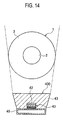
- FIG. 14 shows a light emitting device 400 according to a fourth embodiment of the present invention
- FIGs. 16A and 16B show a light emitting element 40 to be mounted thereon.
- the light emitting device 400 according to the fourth embodiment includes the light emitting element 40 which is mounted in the form of a flip chip type.
- a transparent insulating substrate 401 made of a sapphire substrate or the like is used in the light emitting device 40.
- a crystal growth layer 402 which includes a light emitting layer, which is similar to those of the first to third embodiments, is formed on a surface of the substrate.
- An n electrode 41 and a p electrode 42 are formed respectively in appropriate positions on the crystal growth layer 402.
- the thickness of the transparent insulating substrate 401 is reduced by use of a method such as grinding or polishing. It is made possible to retrieve light through the substrate 401.
- a high-concentration phosphor-containing resin layer 42 is formed on a back surface of the substrate 401 of the light emitting element 40.
- the high-concentration phosphor-containing resin layer 42 is formed on the entire back surface of the substrate 401.
- the light emitting device 400 has a following configuration.
- the light emitting element 40 is mounted and fixed, in the form of the flip chip type, on an upper surface of a concave section of a base 45 while the back surface of the substrate 401, where the high-concentration phosphor-containing resin layer 42 is formed, is placed up.
- the light emitting element 40 is disposed such that light intensity in a direction perpendicular to the upper surface of the base 45 is higher than that in a direction parallel to the upper surface of the base 45.
- a low-concentration phosphor-containing resin section 43 which covers the entire light emitting element 40, is formed by filling the concave section of the base 45 with the second phosphor-containing resin as similar to that of the first to third embodiments, and by curing the resin.
- the light emitting device 400 according to the fourth embodiment is characterized by including the light emitting element 40 mounted in the form of the flip chip type, and the manufacturing method thereof is as follows.
- the n electrode 41 and the p electrode 42 are formed on one side of the light emitting element 40.
- the thickness of the insulating substrate 401 is reduced by use of a method such as grinding or polishing. Light can be retrieved through the substrate 401. Accordingly, it is made possible to form the high-concentration phosphor-containing resin layer 42, which has the phosphor concentration from 20 to 25 w%, on the back surface of the substrate 401 of the light emitting element 40. In this case, there are no electrode regions since the high-concentration phosphor-containing resin layer 42 is formed on the back surface of the substrate 401.
- the first phosphor-containing resin is coated entirely on a light emitting section of the back surface of the transparent insulating substrate 401.
- the high-concentration phosphor-containing resin layer 12 is formed by thermosetting or photocuring the above first phosphor-containing resin as shown in FIG 15.
- the first phosphor-containing resin is similar to those of the aforementioned embodiments, and has the adjusted phosphor concentration.
- the crystal growth wafer 410 is cut out into desired dimensions, such as 0.35 mm on a side, by scribing, dicing or the like, and is thereby split into individual chips respectively constituting the light emitting elements 40.
- each of the light emitting element 40 which is split into a chip, is mounted and fixed on the upper surface of the concave section of the base 45 while the side of the back surface of the substrate 401, where the high-concentration phosphor-containing resin layer 42 is formed, is placed up. Thereafter, the concave section of the transparent insulating substrate 45 is filled with the second phosphor-containing resin by dispensing, and is treated with thermosetting. The low-concentration phosphor-containing resin section 43 is formed.
- the second phosphor-containing resin is formed directly above the light emitting element 40, and has the phosphor concentration lower, for example, from 10 to 15 w%, than that of the high-concentration phosphor-containing resin layer 42. In this way, the light emitting device 400 of the fourth embodiment is obtained.
- the high-concentration phosphor-containing resin layer 42 is formed directly on the back surface of the substrate 401. Accordingly, a positional relation is intact between the high-concentration phosphor-containing resin layer 42 and the light emitting element 40.
- the low-concentration phosphor-containing resin section 43 is formed while covering the light emitting element 40 on which the high-concentration phosphor-containing resin layer 42 is formed.
- the light emitting device 400 of the fourth embodiment also makes it possible to reduce color shading on the light emission observation surface, and to improve the in-plane uniformity irrespective of the shape of the light emitting device such as the round type or the surface mount type.
- FIG 17 shows a light emitting device 500 according to a fifth embodiment of the present invention
- FIGs. 21A and 21B each show a light emitting element 50 to be mounted thereon.
- the light emitting device 500 according to the fifth embodiment is characterized in that a light emitting diode of a substrate replacing type, which has an excellent heat dissipation capacity, is mounted as the light emitting element 50.
- a supporting substrate 511 obtained by replacing a sapphire substrate or a GaN substrate 501 with a crystal growth layer 502 a substance, such as copper tungsten (CuW), which has high heat conductivity and a thermal expansion coefficient close to that of the sapphire substrate or the GaN substrate, is used.
- a p electrode 52 is joined to a back surface of the supporting substrate 511, the crystal growth layer 502 is joined to an upper surface of the supporting substrate 511, and an n electrode 51 is formed on an n-type surface of the crystal growth layer 502.
- a high-concentration phosphor-containing resin layer 55 is formed on the n-type surface.
- the n electrode 51 is formed on the n-type surface of the crystal growth layer 502.
- the high-concentration phosphor-containing resin layer 55 when forming the high-concentration phosphor-containing resin layer 55 in which the phosphor concentration thereof is adjusted to the high concentration of 20 to 25 w%, the high-concentration phosphor-containing resin layer 55 is formed so that the first phosphor-containing resin layer is not formed in the region corresponding to the n electrode 51.
- the high concentration phosphor-containing resin layer 55 is formed by coating the first phosphor-containing resin by use of the method such as dispensing, screen printing or dot printing, and then by thermosetting or photocuring the resin.
- the light emitting element 50 having the above-described structure is mounted and fixed onto an upper surface of a concave section of a base 56 with a conductive adhesive such as Ag paste white the surface of the crystal growth layer 502, where the high-concentration phosphor-containing resin layer 55 is formed, is placed up.
- the light emitting device 50 is disposed such that light intensity in a direction perpendicular to the upper surface of the base 56 is higher than that in a direction parallel to the upper surface of the base 56.
- the concave section of the base 56 is filled with the second phosphor containing resin by dispensing, and is treated with thermosetting.
- the second phosphor-containing resin contains a phosphor concentration lower than that of the high-concentration phosphor-containing resin layer 55, which is formed directly above the light emitting element 50.
- the semiconductor crystal growth layer 502 of the gallium nitride based material is formed on the crystal substrate 501 such as a sapphire substrate or a GaN substrate.
- a crystal growth wafer 510 for a blue or a near ultraviolet LED is fabricated as in the cases of the first to fourth embodiments.
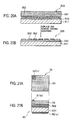
- the sapphire or GaN substrate 501 is replaced with the different supporting substrate 511 to be used as the crystal growth layer 502 for the light emitting element in which the substrate such as the sapphire substrate or the GaN substrate is used, as shown in FIGs. 20A and 20B.
- the above case is particularly for the bigh-flux light emitting element having dimensions of about 1 mm on a side.
- a substance, such as copper tungsten (CuW), which has high heat conductivity and a thermal expansion coefficient close to that of the sapphire substrate or GaN substrate, is effective as the supporting substrate 511 used for a replacement.
- CuW copper tungsten
- the crystal growth layer 502 is replaced with the supporting substrate 511 by use of a bounding layer 512.
- a p-type side of the crystal growth layer 502 is joined to the supporting substrate 511, and the n-type side thereof is a plane surface.
- the n-type side is on a surface on which the high-concentration phosphor-containing resin layer 55 is formed as in the cases of the first to fourth embodiments.
- the high-concentration phosphor-containing resin layer 55 is formed so that the first phosphor-containing resin layer is not formed in the region corresponding to the n electrode 51.
- the high-concentration phosphor-containing resin layer 55 is formed by coating the first phosphor-containing resin by use of the method such as dispensing, screen printing or dot printing, and then by thermosetting or photocuring the resin.
- a crystal growth wafer 520 shown in FIG 20B is cut out into desired dimensions by scribing, dicing or the like, and is thereby split into individual chips respectively constituting the light emitting elements 50.
- each of the light emitting element 50 which is split into a chip, is mounted and fixed on the upper surface of the concave section of the base 56 with a conductive adhesive such as Ag paste while the surface of the crystal growth layer 502 where the high-concentration phosphor-containing resin layer 55 is formed is placed up. Thereafter, by means of bonding, electric conductivity is achieved with a gold wire 57, as in the eases of the first to fourth embodiments.
- the concave section of the base 35 is filled with the second phosphor-containing resin having the phosphor concentration in the range of 10 to 15 w%, and is treated with thermosetting. Thereby, the low-concentration phosphor-containing resin section 58 is formed while covering the periphery and the upper surface of the light emitting element 50. Accordingly, the light emitting device 500 is obtained.
- the light emitting device 500 thus manufactured When the light emitting device 500 thus manufactured is energized to emit light, color shading of the emitted light between the central section 2 and the peripheral section 3 is reduced on the light emission observation surface 1 shown in FIG. 17, and the in-plane uniformity is improved, as in the cases of the first to fourth embodiments.
- the high-concentration phosphor-containing resin layer 55 is formed directly on the surface of the crystal growth layer 502. Accordingly, a positional relation is intact between the high-concentration phosphor-containing resin layer 55 and the light emitting element 50.
- the low-concentration phosphor-containing resin section 58 is formed while covering the light emitting element 50 on which the high-concentration phosphor-containing resin layer 55 is formed.
- the light emitting device 500 of the fifth embodiment also makes it possible to reduce color shading on the light emission observation surface, and to improve the in-plane uniformity irrespective of the shape of the light emitting device such as the round type or the surface mount type.
- FIG. 22 shows a light emitting device 600 according to a sixth embodiment of the present invention
- FIGs. 24A and 24B each show a light emitting element 60 to be mounted thereon.
- the light emitting device 600 according to the sixth embodiment includes the light emitting element 60 which is mounted in the form of the junction-up type.
- the light emitting device 600 has a structure in which at least part of the light emitting element is tapered in order to improve light retrieval, and is disposed such that light intensity in a direction parallel to an upper surface of a base is higher than that in a direction perpendicular to the upper surface of the base.
- a conductive SiC substrate is used as a substrate 601 in the light emitting element 60, for example.
- a crystal growth layer 602 is formed on a surface of the substrate 601, and phosphor-containing transparent resin having a relatively low concentration, such as in a range of 10 to 15 w% (hereinafter referred to as third phosphor-containing transparent resin), is coated on a surface of the crystal growth layer 602.
- the third phosphor-containing transparent resin is then cured to form a low-concentration phosphor-containing resin layer 63.
- a p electrode 61 is formed on a surface of the light emitting element 60 where the low-concentration phosphor-containing resin layer 63 is formed, and an n electrode 62 is formed on an opposite surface of the light emitting element 60.
- the light emitting element 60 of the above-described configuration is mounted and fixed onto a concave section of a base 64 with a conductive adhesive such as Ag paste while the surface of the crystal growth layer 602, where the low-concentration phosphor-containing resin layer 63 is formed, is placed up.
- the light emitting element 600 of the sixth embodiment has a configuration in which a cross-sectional area of the substrate 601 is made smaller than a cross-sectional area of the surface of the crystal growth layer 602 where the low-concentration phosphor-containing resin layer 63 is formed.
- the light emitting element 60 in the sixth embodiment is disposed such that light intensity in a direction parallel to an upper surface of the base 64 is higher than that in a direction perpendicular to the upper surface of the base 64.
- electric conductivity is achieved with a gold wire 65.
- the light emitting device 600 has a following configuration.
- the concave section of the base 35 and surroundings of the light emitting element 60 are filled with phosphor-containing resin having a phosphor concentration higher than that of the low-concentration phosphor-containing resin layer 63 (hereinafter referred to as fourth phosphor-containing transparent resin), and is treated with thermosetting.
- a high-concentration phosphor-containing resin section 66 is formed.
- the high-concentration phosphor-containing resin section 66 has the phosphor concentration in a range of 20 to 25 w%, for instance.
- a semiconductor crystal growth layer of a gallium nitride based material is formed on a conductive crystal substrate made of a SiC substrate to fabricate a crystal growth wafer 610 for blue or ultraviolet LEDs. Thereafter, a fabrication process, such as a process of fabricating an electrode, is performed to form LED structures.
- the wafer 610 After the fabrication process, a large number of LED light emitting element 60 are formed on the wafer 610. Dimensions of the respective LED chips are set to be 0.35 mm on a side, for example. Subsequently, the third phosphor-containing resin is coated on an upper portion of the crystal growth wafer 610, where the LED light emitting element chips are formed, by use of the method such as dispensing, screen printing or dot printing. Thereafter the resin is treated by thermosetting or photocuring. Accordingly, the low-concentration phosphor-containing resin layer 63 is formed.
- the p electrode 61 is formed on a surface where the low-concentration phosphor-containing resin layer 63 is formed in the light emitting element 60 mounted in the sixth embodiment. For this reason, when forming the low-concentration phosphor-containing resin layer 63, which has the adjusted phosphor concentration, on the surface of the crystal growth layer 602 in the light emitting element 60, the high-concentration phosphor-containing resin layer 63 is formed so that the low-concentration phosphor-containing resin layer is not formed in the region corresponding to the n electrode 61.
- the high-concentration phosphor-containing resin layer 63 is formed by coating the third phosphor-containing resin by use of the method such as dispensing, screen printing or dot printing, and then by thermosetting or photocuring the resin.
- the low-concentration phosphor-containing resin layer 63 has the thickness in a range of about 5 to 10 ⁇ m and the phosphor concentration in a range of 10 to 15 w%.
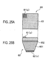
- the crystal growth wafer 610 is cut out into desired dimensions from the substrate 601. Thereby, the crystal growth wafer 610 is split into chips with dimensions of, for example, 0.35 mm on a side, chips respectively constituting individual light emitting elements 60. In this way, a taper can be formed on at least one of side surfaces.
- the shape of the light emitting element 60 may be formed into a shape in which all of the side surfaces of the conductive substrate 601 are tapered downward, as shown in FIG. 25B.
- each of the light emitting element 60 which is split into a chip, is mounted and fixed on the surface of the concave section of the base 64 with a conductive adhesive such as Ag paste while the surface of the crystal growth layer 602, where the low-concentration phosphor-containing resin layer 63 is formed, is placed up.
- a conductive adhesive such as Ag paste
- the concave section of the base 64 and surroundings of the light emitting element 60 are filled with the fourth phosphor-containing resin, and is treated with thermosetting.
- a high-concentration phosphor-containing resin section 66 is formed. Accordingly, the light emitting device 600 is obtained.
- the phosphor concentration of the high-concentration phosphor-containing resin section 66 is in a range of 20 to 25 w%.
- the phosphor concentration of the phosphor-containing transparent resin section 66 which is filled around the light emitting element 60, is set higher than the phosphor concentration of the phosphor-containing transparent resin layer 63 formed directly above the light emitting element 60. This is because the light emitting element 60 is disposed on the upper surface of the base 64 such that the light intensity in the direction parallel to the upper surface of the base is higher than that in the direction perpendicular to the upper surface of the base.
- the light emitting device 600 of the sixth embodiment as shown in FIG 22, the light, which has the high light intensity, and which is emitted in a horizontal direction from the light emitting element 60 to the upper surface of the base 64, is projected to the outside through the high-concentration phosphor-containing resin section 66.
- the light, which has the low light intensity, and which is emitted in the perpendicular direction from the light emitting element 60 to the upper surface of the base 64 is projected to the outside through the low-concentration phosphor-containing resin layer 63.
- the light, which has the high light intensity, and which is emitted in the direction parallel to the upper surface of the base 64 is efficiently converted into light having a different wavelength by the phosphor in the high-concentration phosphor-containing resin section 66.
- the light emitting device 600 of the sixth embodiment causes the white color in the peripheral section 3 as well. In this way, it is made possible to reduce color shading of the emitted light between the central section 2 and the peripheral section 3, and to improve the in-plane uniformity.
- the low-concentration phosphor-containing resin layer 63 is formed directly on the surface of the crystal growth layer 602. Accordingly, a positional relation is intact between the low-concentration phosphor-containing resin layer 63 and the light emitting element 60.
- the high-concentration phosphor-containing resin section 66 is formed while covering the surroundings of the light emitting element 60 on which the low-concentration phosphor-containing resin layer 63 is formed.
- positional relations are also intact respectively between the high-concentration phosphor-containing resin section 66 and the low-concentration phosphor-containing resin layer 64 and between the high-concentration phosphor-containing resin section 66 and the light emitting element 60.
- the structure of the light emitting device 600 according to the sixth embodiment also makes it possible to reduce color shading on the light emission observation surface, and to improve the in-plane uniformity irrespective of the shape of the light emitting device such as a round type or a surface mount type.
- each of the embodiments described above illustrates the light emitting device in which the light emitting element is mounted, the nitride semiconductor being used for the semiconductor crystal growth layer of the light emitting element
- the present invention is not limited to this configuration. It is also possible to adopt a LED light emitting element in which a semiconductor of a zinc oxide type is used.
- the substrate it is possible to use an insulating substrate, such as a sapphire substrate, and a conductive substrate, such as a GaN substrate or a SiC substrate.
- the light emitting device 100 having the structure shown in FIG. 3 is fabricated with the following manufacturing method.
- the semiconductor crystal growth layer 102 of the gallium nitride based material is formed, as the LED light emitting element 10, on the sapphire crystal substrate 101 having the thickness of 250 ⁇ m.
- the crystal growth wafer 110 for blue LEDs is fabricated, and the fabrication process, such as the process of fabricating the electrode, is performed to form LED structures.
- silicon transparent resin containing 25 w% of an oxide phosphor hereinafter referred to as first phosphor-containing silicon resin
- the high-concentration phosphor-containing resin layer 12 having the thickness of 10 ⁇ m is formed by thermosetting the resin.
- the crystal growth wafer 110 is cut out into desired dimensions of 0.35 mm on a side, and is thereby split into individual chips respectively constituting the light emitting elements 10.
- each of the light emitting elements 10, which is split into each chip, is mounted and fixed on the upper surface of the concave section of the base 15, which has the height of 300 ⁇ m and the diameter of 400 ⁇ m, with a conductive adhesive made of Ag paste.
- the gold wires 16 and 17 are respectively connected to the n electrode 13 and the p electrode 14, and the feed pattern is connected to each of the wires 16 and 17.
- the gold wires 16 and 17, n electrode 13, p electrode 14 and the feed pattern are caused to be electrically conductive to one another.
- the concave section of the base 15 is filled with silicon transparent resin (hereinafter referred to as second phosphor-containing silicon resin), and is treated by thermosetting. Thereby, the low-concentration phosphor-containing resin section 18 is formed.
- the second phosphor-containing silicon resin had a phosphor concentration, which is the phosphor concentration of 15 w%, the concentration being lower than that of the high-concentration phosphor-containing resin layer 12 formed on a surface of the semiconductor crystal growth layer 102. In this way, the light emitting device 100 is obtained.
- the light emitting device 200 shown in FIG. 8 is fabricated with the following manufacturing method. As shown in FIG 9, in the light emitting element 20 in which the conductive substrate 201 of GaN substrate having the thickness of 250 ⁇ m, the p electrode 21 is formed on a surface of the first phosphor-containing silicon resin, the surface being one where the high-concentration phosphor-containing resin layer 22 is formed.
- the high-concentration phosphor-containing resin layer 22 is made of the first phosphor-containing silicon resin, which is similar to that of Example 1.
- the high-concentration phosphor-containing resin layer 22 directly above the light emitting element 20 by use of screen printing, the first phosphor-containing silicon resin is coated so that the high-concentration phosphor-containing resin layer is not formed in the region corresponding to the p electrode 21. Accordingly, the high-concentration phosphor-containing resin layer 22 having the thickness of 10 ⁇ m is formed by thermosetting the resin.
- the crystal growth wafer 210 is cut out into desired dimensions, namely, 0.35 mm on a side. Thereby, the crystal growth is split into individual chips respectively constituting the light emitting elements 20.
- each of the light emitting element 20, which is split into a chip is mounted and fixed, in the form of the junction-up type, on the upper surface of the concave section of the base 25, which is similar to that of Example 1, with a conductive adhesive made of Ag paste while facing the crystal growth layer 202 up. Thereafter, by means of bonding, electric conductivity is achieved with the gold wire 23. After that, by means of dispensing, the concave section of the base 25 is filled with the second phosphor-containing silicon resin, which is similar to that of Example 1. Then, the second phosphor-containing silicon resin is treated with thermosetting to form the low-concentration phosphor-containing resin section 24. In this way, the light emitting device 200 is obtained.
- the light emitting device 300 shown in FIG 11 is fabricated with the following manufacturing method. As shown in FIGs. 13A and 13B, as the LED light emitting element 30, the crystal growth layer 302 similar to that of Example 1 is formed on the GaN substrate 301 having the thickness of 250 ⁇ m. Moreover, the p electrode 31 is formed on the surface of the crystal growth layer 302, and the electrode 32 is formed on the back surface of the conductive substrate 301. Thereafter, the high-concentration phosphor-containing resin layer 33, which is made of the first phosphor-containing silicone resin as similar to that of Example 1, is formed to have the thickness of 10 ⁇ m.
- the high-concentration phosphor-containing resin layer 33 is formed on the entire back surface of the conductive substrate 301 except for the region of the n electrode 32.
- the n electrode 32 is formed on the surface where the high-concentration phosphor-containing resin layer 33 made of the first phosphor-containing silicon resin is formed. Accordingly, as shown in FIG. 12, when forming the high-concentration phosphor-containing resin layer 33, which has the adjusted phosphor concentration, on the back surface of the wafer 310, the second phosphor-containing silicon resin is coated on the wafer 310 by use of screen printing so that the high-concentration phosphor-containing resin layer is not formed in the region corresponding to the n electrode 32.
- the high-concentration phosphor-containing resin layer 33 having the thickness of 10 ⁇ m is formed by thermosetting the resin. Thereafter, by means of scribing, the crystal growth wafer 310 is cut out into desired dimensions, namely, 0.35 mm on a side. Thereby, the crystal growth wafer 310 is split into individual chips respectively constituting the light emitting elements 30.
- each of the light emitting element 30, which is split into a chip, is mounted and fixed on the upper surface of the concave section of the base 35 similar to that of Example 1.
- the light emitting elements 30 are fixed in the form of the junction-down type while the side of the back surface of the substrate 301 is placed up.
- electric conductivity is achieved with the gold wire 36.
- the concave section of the base 35 and surroundings of the light emitting element 60 are filled with the second phosphor-containing resin, and is treated with thermosetting.
- a low-concentration phosphor-containing resin section 37 is formed while covering the surroundings, and the upper surface, of the light emitting element 30. Accordingly, the light emitting device 300 is obtained.
- the light emitting device 400 shown in FIG 14 is fabricated with the following manufacturing method.
- the light emitting device 400 included the light emitting element 40 which is mounted in the form of the flip chip type.
- the sapphire insulating substrate 401 having the thickness of 250 ⁇ m is used.
- the semiconductor crystal growth layer 402 similar to that of Example 1 is formed on the surface of the sapphire insulating substrate 401, and the n electrode 41 and the p electrode 42 are formed on the surface of the crystal growth layer 402.
- the transparent sapphire substrate 401 is polished to the thickness of 80 ⁇ m to retrieve light from the substrate 401.
- the first phosphor-containing silicon resin which is similar to that of Example 1, is coated on the entire light emitting section of the back surface of the substrate 401, and is treated by thermosetting.
- the high-concentration phosphor-containing resin 42 is formed in the thickness of 10 ⁇ m, and the crystal growth wafer 410 is thus obtained, as shown in FIG 15.
- the crystal growth wafer 410 is cut out into desired dimensions, namely, 0.35 mm on a side, and is thereby split into individual chips respectively constituting the light emitting elements 40.
- each of the light emitting element 40 which is split into a chip, is mounted and fixed on the upper surface of the concave section of the base 45 similar to that of Example 1.
- the light emitting elements 40 are fixed in the form of the flip chip type while the side of the back surface of the substrate 401, on which the high-concentration phosphor-containing resin layer 42 is formed, is placed up.
- the concave section of the base 45 is filled with the second phosphor-containing silicon resin similar to that of Example 1, and is treated by thermosetting. Accordingly, the low-concentration pbosphor-containing resin section 43 is formed, and the light emitting device 400 is thus obtained.
- the light emitting device 500 shown in FIG. 17 is fabricated with the following manufacturing method.
- the light emitting diode of the substrate replacing type having an excellent heat dissipation capacity is mounted, as the light emitting element 50, on the light emitting device 500 as shown in FIGs. 21A and 21B.
- the semiconductor crystal growth layer 502 of the gallium nitride based material is formed on the crystal substrate 501 made of the sapphire substrate having the thickness of 250 ⁇ m. Thereby, the crystal growth wafer 510 for blue LEDs is fabricated.
- the sapphire substrate 501 is replaced with the different supporting substrate 511 to be used as the crystal growth layer 502. Copper tungsten (CuW) in the thickness of 200 ⁇ m is used as the supporting substrate 511 for a replacement.
- the copper tungsten has high heat conductivity and a thermal expansion coefficient close to that of the sapphire substrate or GaN substrate.
- the crystal growth layer 502 is replaced with the supporting substrate 511 by use of the bounding layer 512 of AuSn in the thickness of 10 ⁇ m.
- the p-type side of the crystal growth layer 502 is joined to the supporting substrate 511, and the n-type side thereof is the plane surface.
- the n-type side is on a surface on which the high-concentration phosphor-containing resin layer 55 is formed as in the cases of Examples 1 to 4. Since the n electrode 51 is formed on the n-type surface, when forming the high-concentration phosphor-containing resin layer 55, the first phosphor-containing silicon resin is coated by use of screen printing so that the high-concentration phosphor-containing resin layer is not formed in the region corresponding to the p electrode 51. Accordingly, the high-concentration phosphor-containing resin layer 55 having the thickness of 10 mm is formed by thermosetting the resin.
- the crystal growth wafer 520 shown in FIG 20B is cut out into desired dimensions, namely, 1 mm on a side, and is thereby split into individual chips respectively constituting the light emitting elements 50, as shown in FIGs. 21A and 21B.
- each of the light emitting element 50 which is split into a chip, is mounted and fixed on the upper surface of the concave section of the base 56 similar to that of Example 1.
- a conductive adhesive made of Ag paste the light emitting elements 50 are fixed while the surface of the crystal growth layer 501 where the high-concentration phosphor-containing resin layer 55 is formed, is placed up.
- bonding electric conductivity is achieved with the gold wire 57 as in the cases of Examples 1 and 2.
- the concave section of the substrate 56 is filled with the second phosphor-containing silicon resin similar to that of Example 1, and is treated by thermosetting.
- the low-concentration phosphor-containing resin section 58 is formed while covering the surroundings, and the upper surface, of the light emitting element 50. Accordingly, the light emitting device 500 is obtained.
- the light emitting device 600 shown in FIG. 22 is fabricated with the following manufacturing method.
- the semiconductor crystal growth layer 602 of the gallium nitride based material is formed on the conductive crystal substrate made of the SiC substrate, and the crystal growth wafer 610 for blue LEDs is fabricated.
- the fabrication process such as the process for fabricating the electrode is performed to form LED structures.
- a large number of LEDs 60 are formed on the wafer 610. Dimensions of each LED chip are set to be 0.35 mm on a side.
- the first phosphor-containing silicon resin which contained 15 w% of an oxide phosphor, is coated on the surface of the crystal growth layer 602 of the crystal growth wafer 610. Accordingly, the low-concentration phosphor-containing resin layer 63 having the thickness of 10 ⁇ m is formed by thermosetting the resin. As shown in FIGs. 24A and 24B, in the light emitting element 60, the p electrode 61 is formed on the surface where the low-concentration phosphor-containing resin layer 63 is formed.
- the silicon transparent resin is coated by use of screen printing so that the low-concentration phosphor-containing resin layer is not formed in the region corresponding to the p electrode 61. Accordingly, the low-concentration phosphor-containing resin layer 63 is formed by thermosetting or photocuring the resin.
- the low-concentration phosphor-containing resin layer 63 had the thickness of 10 ⁇ m.
- the crystal growth wafer 610 is cut out into desired dimensions from the substrate 601, and individual light emitting elements 60 are formed.
- the chip dimensions are set to 0.35 mm on a side. In this way, a taper is provided on at least one of the side surfaces of the light emitting element 60.
- each of the light emitting elements 60 which is split into a chip, is mounted and fixed on the upper surface of the concave section of the base 64 with the dimensions similar to those of Example 1.
- a conductive adhesive made of Ag paste By use of a conductive adhesive made of Ag paste, the light emitting elements 60 are fixed while the surface of the crystal growth layer 602 where the low-concentration phosphor-containing resin layer 63 is formed, is placed up. Thereafter, the concave section of the substrate 64 is filled with the transparent resin with the phosphor concentration of 25 w%, and the high-concentration phosphor-containing resin section 66 is formed. Accordingly, the light emitting device 600 is obtained.
- the transparent resin has a phosphor concentration higher than that of the low-concentration phosphar-containing resin layer 63.
Landscapes
- Led Device Packages (AREA)
- Led Devices (AREA)
- Structures Or Materials For Encapsulating Or Coating Semiconductor Devices Or Solid State Devices (AREA)
Abstract
Description
- This application is based upon and claims the benefit of priority from prior
Japanese Patent Application P2005-280321 filed on September 27, 2005 - The present invention relates to a light emitting device which is provided with a light emitting element and a phosphor, and which is configured to emit light, and a method for manufacturing the light emitting device.
- A known conventional light emitting device, which is provided with a light emitting element and a phosphor, is configured in the following manner, for example. A lead frame, which is provided with a concave section, is used to mount a light emitting diode (LED), which is the light emitting element, on a bottom surface of the concave section of the lead frame. The phosphor is mixed with a transparent resin, and the concave section is fully filled with this phosphor-containing resin so that the resin covers the LED. The phosphor is designed to absorb light emitted from the LED, and is designed to convert the light into light having a different wavelength. Among light emitting devices of this configuration, there is one in which a blue LED is used as the LED and the phosphor configured to convert wavelength of the light for the blue LED into that for yellow is used, for example. Such a light emitting device enables white light to be emitted on a light emission observation surface by mixing the blue light and the yellow light. Meanwhile, in another light emitting device, a near ultraviolet LED is used as the LED and the phosphor configured to convert wavelength of the light for the near ultraviolet LED into those for three colors of red, green, and blue is used. Such a light emitting device enables white light to be emitted on a light emission observation surface by mixing the colors emitted from the phosphor.
- However, in these light emitting devices, depending on the shape of the light emitting element, uneven light emission is caused due to a difference in light intensity of the blue light or the near ultraviolet light emitted from an upper surface side or a side surface side of the light emitting element For example, as shown in FIG 1, a
light emitting device 800 configured in the following manner will be considered. Alight emitting element 80 is mounted in the device, and phosphor-containingtransparent resin 81 fills around the device while contacting and covering the device. Thelight emitting element 80 has a structure in which the light intensity is the highest in a direction directly above the blue LED or the near ultraviolet LED. When thelight emitting device 800 is viewed from a lightemission observation surface 1, anoverhead section 2 of thelight emitting element 80, in which the blue LED or the near ultraviolet LED is used, looks blue or violet due to the blue light or the ultraviolet, and a surroundingsection 3 looks white. Accordingly, this device causes color shading. As shown in FIG 2, there may also be a case in which the light intensity is the highest in a lateral direction and an obliquely downward direction depending on a shape of alight emitting element 90. Consideration will be given for alight emitting device 900 of a configuration in which such alight emitting element 90 is mounted, and in which phosphor-containingtransparent resin 91 fills around the device while contacting and covering the device. In a case where thelight emitting device 900 is viewed from a lightemission observation surface 1, anoverhead section 2 of thelight emitting element 90, in which the blue LED or the near ultraviolet LED is used, looks white, and a surroundingsection 3 exhibits a color in a blue to ultraviolet zone. Accordingly, this device causes color shading. - As a light emitting device with which such color shading can be eliminated, light emitting devices as disclosed in
Japanese Patent Publication No. 2004 - 111882 Patent Document 1") and inJapanese Patent Publication No. 2004 - 349647 Patent Document 2") are known. The light emitting device disclosed inPatent Document 1 has a following configuration. After the light emitting element is mounted on the concave section of the lead frame, first phosphor-containing transparent resin having a low phosphor concentration is filled up to a position of an upper surface of the light emitting element. Second phosphor-containing transparent resin having a high phosphor concentration is disposed on the first phosphor-containing resin. A value, which is obtained by multiplying an optical path length reaching an upper surface of the second phosphor-containing transparent resin by the concentration of the phosphor, is maintained to be constant. Thereby, color shading is reduced. On the other hand, in the light emitting device disclosed inPatent Document 2, a phosphor unit is disposed on a plane of an optical member located inside the light emitting device, the plane facing the light emitting element. In addition, in-plane intensity distribution of the phosphor concentration is provided within the plane. Thereby, color shading is reduced. - However, in the light emitting device disclosed in
Patent Document 1, there is a case where a position for fixing the light emitting element to a concave section of a base is displaced when the light emitting element is mounted on the concave section of the base. In this case, the methods of forming the phosphor-containing resin, which corresponds to the respective conventional techniques described above, likely induce displacement of a layout between the light emitting element and the phosphor-containing resin. A problem, which may occur as a consequence, is that color shading cannot be reduced. Moreover, as in the light emitting device disclosed inPatent Document 2, in a case where the device is configured so that the light emitting element and the phosphor-containing resin are located apart from each other, it is necessary to consider spread of the light emitted from the light emitting element as well. Accordingly, there is a problem that it is technically difficult to control the in-plane intensity distribution for the spreading radiation or for the position to which the light emitting element is fixed. - The present invention has been made in view of the foregoing technical problems of the prior art. An object of the present invention is to provide a light emitting device with which uniform light emission can be obtained on a light emission observation surface, and to provide a method for manufacturing the light emitting device.
- A first aspect of the present invention inheres in a light emitting device which includes a base, a light emitting element, a phosphor-containing transparent resin section, and a high-concentration phosphor-containing resin layer. The light emitting element is disposed on an upper surface of the base so that the light intensity of the light emitting element is higher in a direction perpendicular to the upper surface of the base than in a direction horizontal to the upper surface of the base. The phosphor-containing transparent resin section is provided above the light emitting element while covering an area wider than an upper surface of the light emitting element, and contains the phosphor to which the light emitted from the light emitting element is absorbed, and which emits light having a wavelength different from a wavelength of the absorbed light. The high-concentration phosphor-containing resin layer is formed on an upper surface of the light emitting element, and has a phosphor concentration higher than a phosphor concentration of the phosphor-containing transparent resin section.
- In the light emitting device according to the first aspect, light emitted in the perpendicular direction from the light emitting element may be projected to the outside through the high-concentration phosphor-containing resin layer and through the phosphor-containing transparent resin section, and in which light emitted in the parallel direction from the light emitting element may be projected to the outside through the phosphor-containing transparent resin section.
- In the light emitting device according to the first aspect, the phosphor-containing transparent resin section may have phosphor concentration in a range of 10 to 15 weight percent, and the high-concentration phosphor-containing resin layer may have phosphor concentration in a range of 20 to 25 weight percent
- A second aspect of the present invention inheres in a light emitting device which includes the base, the light emitting element, the phosphor-containing transparent resin, and a low concentration phosphor-containing resin layer. The light emitting element is disposed on the upper surface of the base so that the light intensity of the light emitting element is higher in a direction perpendicular to the upper surface of the base than in a direction horizontal to the upper surface of the base. The phosphor-containing transparent resin section is provided above the light emitting element while covering an area wider than an upper surface of the light emitting element, and contains the phosphor, to which the light emitted from the light emitting element is absorbed, and which emits light having a wavelength different from that of the absorbed light The low-concentration phosphor-containing resin layer is formed on the upper surface of the light emitting element, and has a phosphor concentration lower than a phosphor concentration of the phosphor-containing transparent resin section.
- In the light emitting device according to the second aspect, light emitted in the perpendicular direction from the light emitting element may be projected to the outside through the low-concentration phosphor-containing resin layer, and in which light emitted in the parallel direction from the light emitting element may be projected to the outside through the phosphor-containing transparent resin section.
- In the light emitting device according to the second aspect, the phosphor-containing transparent resin section may have phosphor concentration in a range of 20 to 25 weight percent, and the low-concentration phosphor-containing resin layer may have phosphor concentration in a range of 10 to 15 weight percent.
- In the light emitting device of any one of the first and second aspects, the light emitting element may emit any one of blue light and ultraviolet light.
- A third aspect of the present invention inheres in a method for manufacturing a light emitting device, which includes: forming, on a surface of the light emitting element, a phosphor-containing resin layer containing a phosphor which absorbs light emitted from the light emitting element, and which emits light having a wavelength different from a wavelength of the absorbed light, the light emitting element being disposed on a surface of the substrate and being provided with a light emitting layer, the surface of the light emitting element facing the surface of the substrate; placing the surface of the phosphor-containing resin layer up, and disposing the light emitting element onto an upper surface of a base so that light intensity in a direction perpendicular to the upper surface of the base is higher than that in a direction parallel to the upper surface of the base; and forming a phosphor-containing transparent resin section, which has a phosphor concentration lower than a phosphor concentration of the phosphor-containing resin layer, above the light emitting element while covering an area wider than the surface of the light emitting element where the phosphor-containing resin layer is formed.
- A fourth aspect of the present invention inheres in a method for manufacturing a light emitting device, which includes: forming, on a surface of the light emitting element, a phosphor-containing resin layer containing a phosphor which absorbs light emitted from the light emitting element, and which emits light having a wavelength different from a wavelength of the absorbed light, the light emitting element being disposed on a surface of the substrate and being provided with a light emitting layer, the surface of the light emitting element facing the surface of the substrate; placing the surface of the phosphor-containing resin layer up, and disposing the light emitting element onto the upper surface of the base so that light intensity in a direction parallel to the upper surface of the base is higher than that in a direction perpendicular to the upper surface of the base; and forming a phosphor-containing transparent resin section, which has a phosphor concentration higher than a phosphor concentration of the phosphor-containing resin layer with surroundings of the light emitting element covered therewith.
- In the method according to the fourth aspect, the phosphor-containing transparent resin section may be formed without covering an upper part of the phosphor-containing resin layer therewith.
- According to the present invention, a light emitting device, which is configured in the following manner, and a manufacturing method thereof can be provided. A light emitting element is disposed on the upper surface of the base so that light intensity in a direction perpendicular to the upper surface of the base is higher than that in a direction horizontal to the upper surface of the base. A phosphor-containing transparent resin section containing a phosphor is provided above the light emitting element while covering an area wider than an upper surface of the light emitting element, absorbs light emitted from the light emitting element, and emits light having a wavelength different from that of the absorbed light. A high-concentration phosphor-containing resin layer has a phosphor concentration higher than that of the phosphor-containing transparent resin section. Thus, phosphor-containing transparent resin, which has a conventional concentration, is adapted as the low-concentration phospbor-containing transparent resin section, and phosphor-containing transparent resin, which has a higher phosphor concentration, is adapted as the high-concentration phosphor-containing resin layer on the upper surface of the light emitting element. Thereby, wavelength of the light, which is radiated from the light emitting element toward the upper surface, can be converted effectively by use of the transparent resin layer having the higher phosphor concentration. Moreover, it is made possible to radiate light, which has the wavelength substantially equivalent to the wavelength converted by use of the low-concentration phosphor-containing transparent resin section around the light emitting element. Accordingly, it is made possible to provide the light emitting device, which has fine in-plane uniformity, and in which color shading of emitted light is reduced.
- In addition, according to the present invention, a light emitting device, which is configured in the following manner, and a manufacturing method thereof can be provided. A light emitting element is disposed on the upper surface of the base so that light intensity in a direction horizontal to the upper surface of the base is higher than that in a direction perpendicular to the upper surface of the base. A phosphor-containing transparent resin section containing a phosphor is provided on the upper surface of the light emitting element while covering surroundings of the light emitting element, absorbs light emitted from the light emitting element, and emits light having a wavelength different from that of the absorbed light A low-concentration phosphor-containing resin layer has a phosphor concentration lower than that of the phosphor-containing transparent resin section. Accordingly, phosphor-containing transparent resin, which has a conventional concentration, is adapted as the low-concentration phosphor-containing resin layer on the upper surface of the light emitting element, and resin, which has a phosphor concentration higher than that of the above conventional concentration, is adopted as the phosphor-containing transparent resin section covering the surroundings of the light emitting element. Thereby, wavelength of the light, which is radiated from the light emitting element in the parallel direction, can be converted effectively by use of the phosphor-containing transparent resin section having the higher phosphor concentration. Moreover, it is made possible to radiate light, which has the wavelength substantially equivalent to the wavelength converted by use of the low-concentration phosphor-containing resin layer on the upper surface of the light emitting element. Accordingly, it is made possible to provide the light emitting device, which has fine in-plane uniformity, and in which color shading of the emitted light is reduced on the optical observation surface.
- Moreover, according to the present invention, any one of the high-concentration phosphor-containing resin layer and the low-concentration phosphor-containing resin layer are formed on the upper surface of the light emitting element. The phosphor-containing transparent resin section is formed while covering either the upper surface, or the surroundings, of the light emitting element. Hence, positional relations are intact respectively between the light emitting element and the high-concentration phosphor-containing resin layer and between the light emitting element and the low-concentration phosphor-containing resin layer. Furthermore, positional relations are also intact respectively between the high-concentration phosphor-containing resin layer and the phosphor-containing transparent resin section, between the low-concentration phosphor-containing resin layer and the phosphor-containing transparent resin section, and between the phosphor-containing transparent resin section and the light emitting element. As a result, the present invention can provide a light emitting device with reduced color shading at a high yield.
- IN THE DRAWINGS:
- FIG 1 is a cross-sectional view of a light emitting device of a related example, FIG. 1 serving as an explanatory drawing for a light emission characteristic of the light emitting device.
- FIG. 2 is a cross-sectional view of a light emitting device of another related example, FIG 2 serving as an explanatory drawing for a light emission characteristic of the light emitting device.
- FIG 3 is a cross-sectional view of a light emitting device according to a first embodiment of the present invention, FIG. 3 serving as an explanatory drawing for a light emission characteristic of the light emitting device.
- FIG. 4 is a cross-sectional view of a semiconductor wafer used for fabricating a light emitting element to be mounted on the light emitting device according to the first embodiment.
- FIG 5 is a perspective view of the wafer after a process of fabricating the light emitting element to be mounted on the light emitting device according to the first embodiment.
- FIG 6 is a perspective view of the wafer after forming a high-concentration phosphor-containing resin layer on the light emitting element to be mounted on the light emitting device according to the first embodiment.
- FIG. 7A is a plan view, and FIG 7B is a cross-sectional view, of the light emitting element to be mounted on the light emitting device according to the first embodiment.
- FIG. 8 is a cross-sectional view of a light emitting device according to a second embodiment of the present invention, FIG. 8 serving as an explanatory drawing for a light emission characteristic of the light emitting device.
- FIG. 9 is a perspective view of a wafer after forming a high-concentration phosphor-containing resin layer on a light emitting element to be mounted on the light emitting device according to the second embodiment.
- FIG 10A is a plan view, and FIG 10B is a cross-sectional view, of the light emitting element to be mounted on the light emitting device according to the second embodiment.
- FIG 11 is a cross-sectional view of a light emitting device according to a third embodiment of the present invention, FIG. 11 serving as an explanatory drawing for a light emission characteristic of the light emitting device.
- FIG 12 is a perspective view of a wafer after forming a high-concentration phosphor-containing resin layer on a light emitting element to be mounted on the light emitting device according to the third embodiment.
- FIG. 13A is a plan view, and FIG 13B is a cross-sectional view, of the light emitting element to be mounted on the light emitting device of the third embodiment.
- FIG 14 is a cross-sectional view of a light emitting device according to a fourth embodiment of the present invention, FIG 14 serving as an explanatory drawing for a light emission characteristic of the light emitting device.
- FIG. 15 is a perspective view of a wafer after forming a high-concentration phosphor-containing resin layer on a light emitting element to be mounted on the light emitting device according to the fourth embodiment.
- FIG. 16A is a plan view, and FIG. 16B is a cross-sectional view, of the light emitting element to be mounted on the light emitting device of the fourth embodiment.
- FIG 17 is a cross-sectaonal view of a light emitting device according to a fifth embodiment of the present invention, FIG. 17 serving as an explanatory drawing for a light emission characteristic of the light emitting device.
- FIG 18 is a cross-sectional view of a semiconductor wafer used for fabricating a light emitting element to be mounted on the light emitting device according to the fifth embodiment.
- FIG 19 is a perspective view of the wafer after a process of fabricating the light emitting element to be mounted on the light emitting device according to the fifth embodiment.
- FIGs. 20A and 20B are respectively cross-sectional views of the wafer in a process of replacing a substrate in a method for manufacturing the light emitting device according to the fifth embodiment, FIG. 20A being the view before replacing the substrate, and FIG 20B being the view after replacing the substrate.
- FIG 21A is a plan view, and FIG. 21B is a cross-sectional view, of the light emitting element to be mounted on the light emitting device according to the fifth embodiment.
- FIG 22 is a cross-sectional view of a light emitting device according to a sixth embodiment of the present invention, FIG. 22 serving as an explanatory drawing for a light emission characteristic of the light emitting device.
- FIG 23 is a perspective view of a wafer after forming a high-concentration phosphor-containing resin layer on a light emitting element to be mounted on the light emitting device according to the sixth embodiment.
- FIG 24A is a plan view, and FIG 24B is a cross-sectional view, of the light emitting element to be mounted on the light emitting device according to the sixth embodiment.
- FIG 25A is a plan view, and FIG. 25B is a cross-sectional view, of another example of the light emitting element to be mounted on the light emitting device according to the sixth embodiment.
- Various embodiments of the present invention will be described with reference to the accompanying drawings. It is to be noted that the same or similar reference numerals are applied to the same or similar parts and elements throughout the drawings, and the description of the same or similar parts and elements will be omitted or simplified.
- FIG. 3 shows a
light emitting device 100 according to a first embodiment of the present invention, and FIGs. 7A and 7B each shows a light emitting diode (LED)light emitting element 10 to be mounted thereon. The LEDlight emitting element 10 has a configuration in which acrystal growth layer 102 is formed on a surface of asapphire crystal substrate 101, and in which a negative (n)electrode 13 and a positive (p)electrode 14 are respectively formed in appropriate positions. Thecrystal growth layer 102 is a gallium nitride based material, and includes a light emitting layer. A high-concentration phosphor-containingresin layer 12 is formed on an upper surface of thecrystal growth layer 102. The high-concentration phosphor-containingresin layer 12 is made of transparent resin containing a high concentration of a phosphor (hereinafter referred to as "first phosphor-containing resin"). - The
light emitting element 10 is mounted, in the form of a junction-up type, on an upper surface of a concave section of a base 15 in which a side, where thecrystal growth layer 102 is formed, is placed up. Thus, in the first embodiment, the LEDlight emitting element 10 is disposed such that light intensity in a direction perpendicular to the upper surface of thebase 15 is higher than that in a direction parallel to the upper surface of thebase 15. - The
light emitting device 100 has a following configuration. Thelight emitting element 10 is disposed on the upper surface of the concave section of thebase 15. By means of bonding,wires n electrode 13 and thep electrode 14, and a feed pattern (not shown) is connected to each of thewires resin section 18, which covers the entirelight emitting element 10, is formed by filling the concave section of the base 15 with transparent resin containing a concentration of the phosphor lower than that of the first phosphor-containing resin (hereinafter referred to as "second phosphor-containing resin"). - The phosphor concentration of the second phosphor-containing resin having a lower phosphor concentration is substantially equivalent to that of phosphor-containing transparent resin which has been conventionally applied to a LED light emitting element of a similar type. For example, the concentration is set in a range of 10 to 15 w%. As described later, the phosphor concentration of the first phosphor-containing resin, which has a higher concentration, is adjusted to an appropriate concentration for achieving in-plane uniformity of emitted colors on a light
emission observation surface 1 of thelight emitting device 100, e.g., in a range of 20 to 25 w%. - Next, descriptions will be provided for a method for manufacturing the
light emitting device 100 having the above-described configuration. First, as shown in FIG. 4, semiconductorcrystal growth layer 102 of the gallium nitride based material is formed, as the LEDlight emitting element 10, on thecrystal substrate 101 made of a sapphire substrate. Acrystal growth wafer 110 for blue or near ultraviolet LEDs is fabricated. A fabrication process, such as a process of fabricating an electrode, is performed to form LED structures. After the fabrication process, the respective LED structures are formed on thewafer 110, as shown in FIG 5. Subsequently, as shown in FIG 6, by use of a method such as dispensing, screen printing or dot printing, transparent resin is coated on a surface facing a surface of thecrystal growth wafer 110, the surface being that of the semiconductorcrystal growth layer 102 in the first embodiment. The above transparent resin is the first phosphor-containing resin in the first embodiment, and contains a higher concentration of a phosphor than that of a usual case. The high-concentration phosphor-containingresin layer 12 is formed by thermosetting or photocuring the above transparent resin. - The
light emitting element 10 adopted in the first embodiment is a light emitting diode of a junction-up mounting type, and uses the insulatingsubstrate 101 made of the sapphire substrate. Accordingly, as shown in FIGs. 7A and 7B, both of then electrode 13 and thep electrode 14 are formed on the surface where the high-concentration phosphor-containingresin layer 12 is formed. For this reason, when forming the high-concentration phosphor-containingresin layer 12, in which the phosphor concentration thereof is adjusted to the high concentration of 20 to 25 w%, on the surface of the semiconductorcrystal growth layer 102, the high-concentration phosphor-containingresin layer 12 is formed so that the high-concentration phosphor-containingresin layer 12 is not formed in the regions corresponding to therespective electrodes resin layer 12 is formed by coating the uncured first phosphor-containing resin by use of the method such as dispensing, screen printing or dot printing, and then by thermosetting or photocuring the resin. Thereafter, thecrystal growth wafer 110 is cut out into desired dimensions by scribing, dicing or the like, and is thereby split into individual chips respectively constituting thelight emitting elements 10. Each side of an L chip has a length of 0.35 mm, for example. - Next, as shown in FIG. 3, each of the
light emitting elements 10, which is split into a chip, is mounted and fixed, in the form of the junction-up type, on the surface of the concave section of the base 15 with a conductive adhesive such as Ag paste while placing thecrystal growth layer 102 up. By means of bonding, electric conductivity is achieved with thegold wires base 15 is filled with the second phosphor containing resin by dispensing, and is treated with thermosetting. The low-concentration phosphor-containingresin section 18 is formed. The second phosphor-containing resin has a phosphor concentration of 10 to 15 w%, which is lower than that of the high-concentration phosphor-containingresin layer 12 formed on the surface of the semiconductorcrystal growth layer 102. Accordingly, thelight emitting device 100 is obtained. - As shown in FIG. 3, when the
light emitting device 100 thus manufactured is energized to be caused to emit light, color shading of the emitted light is reduced on the lightemission observation surface 1, and the in-plane uniformity is improved. Specifically, as shown in FIG. 3, in thelight emitting device 100 of the first embodiment, light, which has high light intensity, and which is emitted from thelight emitting element 10 in a direction perpendicular to the upper surface of thebase 15, is projected to the outside through the high-concentration phosphor-containingresin layer 12. On the other hand, light, which has low light intensity, and which is emitted from thelight emitting element 10 in a direction parallel to the upper surface of thebase 15, is projected to the outside through the low-concentration phosphor-containingresin section 18. Hence, the light, which has the high light intensity, and which is emitted from thelight emitting element 10 in the direction perpendicular to the upper surface of thebase 15, is converted effectively into light having a different wavelength by the phosphor in the high-concentration phosphor-containingresin layer 12. Consequently, as compared to the conventional case, in which thecentral section 2 of the lightemission observation surface 1 is heavily tinted by a blue to a near ultraviolet color, and in which theperipheral section 3 exhibits a white color, as shown in FIG 1, thelight emitting device 100 of the first embodiment causes the white color in thecentral section 2 as well. In this way, it is made possible to reduce color shading of the emitted light between thecentral section 2 and theperipheral section 3, and thereby to improve the in-plane uniformity. - In the first embodiment, the high-concentration phosphor-containing
resin layer 12 is formed directly on the surface of thecrystal growth layer 102. Accordingly, a positional relation is intact between the high-concentration phosphor-containingresin layer 12 and thelight emitting element 10. Furthermore, the low-concentration phosphor-containingresin section 18 is formed while covering thelight emitting element 10 on which the high-concentration phosphor-containingresin layer 12 is formed. Thereby, positional relations are also intact respectively between the low-concentration phosphor-containingresin section 18 and the high-concentration phosphor-containingresin layer 12 and between the low-concentration phosphor-containingresin section 18 and thelight emitting element 10. It is made possible to obtain the light emitting device with which the color shading of the emitted light is reduced, and with which the in-plane uniformity of the emitted colors is improved, at a high yield. - Note that the structure of the
light emitting device 100 of the first embodiment makes it possible to reduce color shading on the light emission observation surface, and to improve the in-plane uniformity irrespective of the shape of the light emitting device such as a round type or a surface mount type. - FIG. 8 shows a
light emitting device 200 according to a second embodiment of the present invention, and FIGs. 10A and 10B each show a LEDlight emitting element 20 to be mounted thereon. The LEDlight emitting element 20 according to the second embodiment is a light emitting element configured to have light intensity in the perpendicular direction higher than that in the parallel direction. The LEDlight emitting element 20 includes acrystal growth layer 202 of a gallium nitride based material,a p electrode 21, and an n electrode. Thecrystal growth layer 202 includes a light emitting layer formed on a surface of aconductive substrate 201 such as a GaN substrate. Thep electrode 21 is formed in an appropriate position on a surface of thecrystal growth layer 202. The n electrode is formed in an appropriate position on a back surface of theconductive substrate 201. A high-concentration phosphor-containingresin layer 22, which is made of the first phosphor-containing resin having the high concentration of the phosphor, is formed on an upper surface of thecrystal growth layer 202. Thelight emitting element 20 is mounted, in the form of a junction-up type, on an upper surface of abase 25, in which a side where thecrystal growth layer 202 is formed is placed up. Hence, in the second embodiment, thelight emitting element 20 is disposed such that light intensity in a direction perpendicular to the upper surface of thebase 25 is higher than that in a direction parallel to the upper surface of thebase 25. - Moreover, the
light emitting device 200 has a following configuration. Thelight emitting element 20 is disposed on an upper surface of the concave section of thebase 25. Awire 23 is connected to thep electrode 21 and to a feed pattern (not shown) by bonding. Furthermore, a low-concentration phosphor-containingresin section 24, which covers the entirelight emitting element 20, is formed by filling the concave section of the base 25 with the second phosphor-containing resin having the concentration of the phosphor lower than that of the first phosphor-containing resin. Incidentally, the phosphor concentration of the second phosphor-containing resin, which has the lower phosphor concentration, and the phosphor concentration of the first phosphor-containing resin, which has the high phosphor concentration, are set similar to those in the first embodiment - Next, descriptions will be provided for a method for manufacturing the
light emitting device 200 according to the second embodiment having the above-described configuration. As shown in FIG. 9, in thelight emitting element 20 using theconductive substrate 201 made of the GaN substrate, thep electrode 21 is formed on a surface where the high-concentration phosphor-containingresin layer 22 made of the first phosphor-containing resin is formed. For this reason, when forming the high-concentration phosphor-containingresin layer 22, in which the phosphor concentration thereof is adjusted to the high concentration from 20 to 25 w%, on the surface of thecrystal growth layer 202, the high-concentration phosphor-containingresin layer 22 is formed so that the high-concentration phosphor-containingresin layer 22 is not formed in the region corresponding to thep electrode 21. The high concentration phosphor-containingresin layer 22 is formed by coating the first phosphor-containing resin by use of the method such as dispensing, screen printing or dot printing, and then by thermosetting or photocuring the resin. Thereafter, thecrystal growth wafer 210 is cut out into desired dimensions, such as 0.35 mm on a side, by scribing, dicing or the like, and is thereby split into individual chips respectively constituting thelight emitting elements 20. - Subsequently, as shown in FIG. 8, each of the
light emitting element 20, which is split into a chip, is mounted and fixed, in the form of the junction-up type, on the concave section of the base 25 with a conductive adhesive such as Ag paste while placing thecrystal growth layer 202 up. By means of bonding, electric conductivity is achieved with thegold wire 23. Subsequently, the concave section of thebase 25 is filled with the second phosphor containing resin by dispensing, and is treated with thermosetting. The low-concentration phosphor containingresin section 24 is formed. The second phosphor-containing resin contains a phosphor concentration lower than that of the high-concentration phosphor-containingresin layer 22, which is formed on the surface of the semiconductorcrystal growth layer 202. Accordingly, thelight emitting device 200 is obtained. - When the
light emitting device 200 thus manufactured is energized to emit light, color shading of the emitted light between thecentral section 2 and theperipheral section 3 is reduced on the lightemission observation surface 1, shown in FIG 8, and the in-plane uniformity is improved as in the case of the first embodiment. In the second embodiment, the high-concentration phosphor-containingresin layer 22 is formed directly on the surface of thecrystal growth layer 202. Accordingly, a positional relation is intact between the high-concentration phosphor-containingresin layer 22 and thelight emitting element 20. The low-concentration phosphor-containingresin section 24 is formed while covering thelight emitting element 20 on which the high-concentration phosphor-containingresin layer 22 is formed. Hence, positional relations are also intact respectively between the low-concentration phosphor-containingresin section 24 and the high-concentration phosphor-containingresin layer 22 and between the low-concentration phasphor-containingresin section 24 and thelight emitting element 20. It is made possible to obtain thelight emitting device 200 with which the color shading of the emitted light is reduced, and with which the in-plane uniformity of the emitted colors is improved, at a high yield. - Note that the
light emitting device 200 of the second embodiment also makes it possible to reduce color shading on the light emission observation surface, and to improve the in-plane uniformity irrespective of the shape of the light emitting device such as the round type or the surface mount type. - FIG 11 shows a
light emitting device 300 according to a third embodiment of the present invention, and FIGs. 13A and 13B each show alight emitting element 30 to be mounted thereon. In thelight emitting device 300 according to the third embodiment, thelight emitting element 30 is mounted and disposed in the form of a junction-down type. As shown in detail in FIGs. 13A and 13B, the LEDlight emitting element 30 includes acrystal growth layer 302 of a gallium nitride based material,a p electrode 31, and ann electrode 32. Thecrystal growth layer 302 includes a light emitting layer formed on a surface of aconductive substrate 301 such as a GaN substrate. Thep electrode 31 is formed in an appropriate position on a surface of thecrystal growth layer 302. Then electrode 32 is formed on a back surface of theconductive substrate 301. A high-concentration phosphor-containingresin layer 33, which is made of the first phosphor-containing resin as similar to those in the first and second embodiments, is formed on the back surface of theconductive substrate 301. Thelight emitting element 30 is mounted, in the form of the junction-down type, on an upper surface of abase 35, in which the back surface side of thesubstrate 301 where the high-concentration phosphor-containingresin layer 33 is formed is placed up. Hence, in the third embodiment, thelight emitting element 30 is disposed such that light intensity in a direction perpendicular to the upper surface of thebase 35 is higher than that in a direction parallel to the upper surface of thebase 35. - As shown in detail in FIG. 11, the
light emitting device 300 has a following configuration. Thelight emitting element 30 is disposed on an upper surface of a concave section of thebase 35. By means of bonding, awire 36 is connected to then electrode 32 and to a feed pattern (not shown). Furthermore, a low-concentration phosphor-containingresin section 37, which covers the entirelight emitting element 30, is formed by filling the concave section of the base 35 with the second phosphor-containing resin as similar to that of the first and second embodiments, and by curing the resin. - Next, descriptions will be provided for a method for manufacturing the
light emitting device 300 according to the third embodiment having the above-described configuration. As shown in FIGs. 13A and 13B, in thelight emitting element 30 using theconductive substrate 301 made of the GaN substrate, then electrode 32 is formed on the surface where the high-concentration phosphor-containingresin layer 33 made of the first phosphor-containing resin is formed. For this reason, as shown in FIG. 12, when forming the high-concentration phosphor-containingresin layer 33, which has the adjusted phosphor concentration on the back surface of thewafer 310, the high-concentration phosphor-containingresin layer 33 is formed so that the high-concentration phosphor-containingresin layer 33 is not formed in the region corresponding to thep electrode 32. The high concentration phosphor-containingresin layer 33 is formed by coating the second phosphor-containing resin by use of the method such as dispensing, screen printing or dot printing, and then by thermosetting or photocuring the resin. Thecrystal growth wafer 310 is cut out into desired dimensions, such as 0.35 mm on a side, by scribing, dicing or the like, and is thereby split into individual chips respectively constituting thelight emitting elements 30. - Next, as shown in FIG 11, each of the
light emitting element 30, which is split into a chip, is mounted and fixed, in the form of the junction-down type, on the concave section of the base 35 with a conductive adhesive such as Ag paste while placing the back surface side of thesubstrate 301 up. By means of bonding, electric conductivity is achieved with thegold wire 36. The concave section of thebase 35 is filled with the second phosphor containing resin by dispensing, and is treated with thermosetting. The low-concentration phosphor-containingresin section 37 is formed with the periphery and the upper surface of thelight emitting element 30 covered therewith. Accordingly, thelight emitting device 300 is obtained. - When the
light emitting device 300 thus manufactured is energized to emit light, color shading of the emitted light between thecentral section 2 and theperipheral section 3 is reduced on the lightemission observation surface 1, shown in FIG 11, and the in-plane uniformity is improved as in the cases of the first and second embodiments. In the third embodiment, the high-concentration phosphor-containingresin layer 33 is formed directly on the back surface of theconductive substrate 301. Accordingly, a positional relation is intact between the high-concentration phosphor-containingresin layer 33 and thelight emitting element 30. The low-concentration phosphor-containingresin section 37 is formed while covering thelight emitting element 30 on which the high-concentration phosphor-containingresin layer 33 is formed. Accordingly, positional relations are also intact respectively between the low-concentration phosphor-containingresin section 37 and the high-concentration phosphor-containingresin layer 33 and between the low-concentration phosphor-containingresin section 37 and thelight emitting element 30. It is made possible to obtain thelight emitting device 300 with which the color shading of the emitted light is reduced, and with which the in-plane uniformity of the emitted colors is improved, at a high yield. - Note that the
light emitting device 300 of the third embodiment also makes it possible to reduce color shading on the light emission observation surface, and to improve the in-plane uniformity irrespective of the shape of the light emitting device such as the round type or the surface mount type. - FIG. 14 shows a
light emitting device 400 according to a fourth embodiment of the present invention, and FIGs. 16A and 16B show alight emitting element 40 to be mounted thereon. Thelight emitting device 400 according to the fourth embodiment includes thelight emitting element 40 which is mounted in the form of a flip chip type. - As shown in detail in FIGs. 16A and 16B, a transparent insulating
substrate 401 made of a sapphire substrate or the like is used in thelight emitting device 40. Acrystal growth layer 402, which includes a light emitting layer, which is similar to those of the first to third embodiments, is formed on a surface of the substrate. Ann electrode 41 anda p electrode 42 are formed respectively in appropriate positions on thecrystal growth layer 402. The thickness of the transparent insulatingsubstrate 401 is reduced by use of a method such as grinding or polishing. It is made possible to retrieve light through thesubstrate 401. - As in the cases of the first to third embodiments, a high-concentration phosphor-containing
resin layer 42 is formed on a back surface of thesubstrate 401 of thelight emitting element 40. In the case of thelight emitting element 40, there are no electrode regions because a surface constituting the high-concentration phosphor-containingresin layer 42 is formed on the back surface of thesubstrate 401. Accordingly, the high-concentration phosphor-containingresin layer 42 is formed on the entire back surface of thesubstrate 401. - As shown in detail in FIG 14, the
light emitting device 400 has a following configuration. By gold bump bonding or the like, thelight emitting element 40 is mounted and fixed, in the form of the flip chip type, on an upper surface of a concave section of a base 45 while the back surface of thesubstrate 401, where the high-concentration phosphor-containingresin layer 42 is formed, is placed up. Accordingly, also in the fourth embodiment, thelight emitting element 40 is disposed such that light intensity in a direction perpendicular to the upper surface of thebase 45 is higher than that in a direction parallel to the upper surface of thebase 45. Furthermore, a low-concentration phosphor-containingresin section 43, which covers the entirelight emitting element 40, is formed by filling the concave section of the base 45 with the second phosphor-containing resin as similar to that of the first to third embodiments, and by curing the resin. - Next, descriptions will be provided for a method for manufacturing the
light emitting device 400 according to the fourth embodiment having the above-described configuration. Thelight emitting device 400 according to the fourth embodiment is characterized by including thelight emitting element 40 mounted in the form of the flip chip type, and the manufacturing method thereof is as follows. - As shown in FIGs. 16A and 16B, in the
light emitting element 40 in which the insulatingsubstrate 401 made of the sapphire substrate is used, then electrode 41 and thep electrode 42 are formed on one side of thelight emitting element 40. The thickness of the insulatingsubstrate 401 is reduced by use of a method such as grinding or polishing. Light can be retrieved through thesubstrate 401. Accordingly, it is made possible to form the high-concentration phosphor-containingresin layer 42, which has the phosphor concentration from 20 to 25 w%, on the back surface of thesubstrate 401 of thelight emitting element 40. In this case, there are no electrode regions since the high-concentration phosphor-containingresin layer 42 is formed on the back surface of thesubstrate 401. By use of a method such as dispensing, screen printing or dot printing, the first phosphor-containing resin is coated entirely on a light emitting section of the back surface of the transparent insulatingsubstrate 401. The high-concentration phosphor-containingresin layer 12 is formed by thermosetting or photocuring the above first phosphor-containing resin as shown in FIG 15. The first phosphor-containing resin is similar to those of the aforementioned embodiments, and has the adjusted phosphor concentration. Thecrystal growth wafer 410 is cut out into desired dimensions, such as 0.35 mm on a side, by scribing, dicing or the like, and is thereby split into individual chips respectively constituting thelight emitting elements 40. - Then, as shown in FIG. 14, by use of a method such as gold bump bonding, each of the
light emitting element 40, which is split into a chip, is mounted and fixed on the upper surface of the concave section of the base 45 while the side of the back surface of thesubstrate 401, where the high-concentration phosphor-containingresin layer 42 is formed, is placed up. Thereafter, the concave section of the transparent insulatingsubstrate 45 is filled with the second phosphor-containing resin by dispensing, and is treated with thermosetting. The low-concentration phosphor-containingresin section 43 is formed. The second phosphor-containing resin is formed directly above thelight emitting element 40, and has the phosphor concentration lower, for example, from 10 to 15 w%, than that of the high-concentration phosphor-containingresin layer 42. In this way, thelight emitting device 400 of the fourth embodiment is obtained. - As shown in FIG 14, when the
light emitting device 400 thus manufactured is energized to emit light, color shading of the emitted light between thecentral section 2 and theperipheral section 3 is reduced on the lightemission observation surface 1, and the in-plane uniformity is improved as in the cases of the first to third embodiments. In the fourth embodiment, the high-concentration phosphor-containingresin layer 42 is formed directly on the back surface of thesubstrate 401. Accordingly, a positional relation is intact between the high-concentration phosphor-containingresin layer 42 and thelight emitting element 40. The low-concentration phosphor-containingresin section 43 is formed while covering thelight emitting element 40 on which the high-concentration phosphor-containingresin layer 42 is formed. Thus, positional relations are also intact respectively between the low-concentration phosphor-containingresin section 43 and the high-concentration phosphor-containingresin layer 42 and between the low-concentration phosphor-containingresin section 43 and thelight emitting element 40. Hence, it is made possible to obtain thelight emitting device 400 with which the color shading of the emitted light is reduced, and the in-plane uniformity of the emitted colors is improved, at a high yield. - Note that the
light emitting device 400 of the fourth embodiment also makes it possible to reduce color shading on the light emission observation surface, and to improve the in-plane uniformity irrespective of the shape of the light emitting device such as the round type or the surface mount type. - FIG 17 shows a
light emitting device 500 according to a fifth embodiment of the present invention, and FIGs. 21A and 21B each show alight emitting element 50 to be mounted thereon. Thelight emitting device 500 according to the fifth embodiment is characterized in that a light emitting diode of a substrate replacing type, which has an excellent heat dissipation capacity, is mounted as thelight emitting element 50. - As a supporting
substrate 511 obtained by replacing a sapphire substrate or aGaN substrate 501 with acrystal growth layer 502, a substance, such as copper tungsten (CuW), which has high heat conductivity and a thermal expansion coefficient close to that of the sapphire substrate or the GaN substrate, is used. Ap electrode 52 is joined to a back surface of the supportingsubstrate 511, thecrystal growth layer 502 is joined to an upper surface of the supportingsubstrate 511, and ann electrode 51 is formed on an n-type surface of thecrystal growth layer 502. A high-concentration phosphor-containingresin layer 55 is formed on the n-type surface. Then electrode 51 is formed on the n-type surface of thecrystal growth layer 502. Accordingly, when forming the high-concentration phosphor-containingresin layer 55 in which the phosphor concentration thereof is adjusted to the high concentration of 20 to 25 w%, the high-concentration phosphor-containingresin layer 55 is formed so that the first phosphor-containing resin layer is not formed in the region corresponding to then electrode 51. The high concentration phosphor-containingresin layer 55 is formed by coating the first phosphor-containing resin by use of the method such as dispensing, screen printing or dot printing, and then by thermosetting or photocuring the resin. - As shown in FIG. 17, in the
light emitting device 500 of the fifth embodiment, thelight emitting element 50 having the above-described structure is mounted and fixed onto an upper surface of a concave section of a base 56 with a conductive adhesive such as Ag paste white the surface of thecrystal growth layer 502, where the high-concentration phosphor-containingresin layer 55 is formed, is placed up. Hence, also in the fifth embodiment, thelight emitting device 50 is disposed such that light intensity in a direction perpendicular to the upper surface of thebase 56 is higher than that in a direction parallel to the upper surface of thebase 56. Furthermore, the concave section of thebase 56 is filled with the second phosphor containing resin by dispensing, and is treated with thermosetting. Thereby, the low-concentration phosphor-containingresin section 58 is formed. The second phosphor-containing resin contains a phosphor concentration lower than that of the high-concentration phosphor-containingresin layer 55, which is formed directly above thelight emitting element 50. - Subsequently, descriptions will be provided for a method for manufacturing the
light emitting device 500 of the fifth embodiment. As shown in FIGs. 18 and 19, in the method for manufacturing the light emitting device of the fifth embodiment, the semiconductorcrystal growth layer 502 of the gallium nitride based material is formed on thecrystal substrate 501 such as a sapphire substrate or a GaN substrate. Thereby, acrystal growth wafer 510 for a blue or a near ultraviolet LED is fabricated as in the cases of the first to fourth embodiments. - As a countermeasure for heat radiation, and for reducing an operating voltage, the sapphire or
GaN substrate 501 is replaced with the different supportingsubstrate 511 to be used as thecrystal growth layer 502 for the light emitting element in which the substrate such as the sapphire substrate or the GaN substrate is used, as shown in FIGs. 20A and 20B. The above case is particularly for the bigh-flux light emitting element having dimensions of about 1 mm on a side. For example, a substance, such as copper tungsten (CuW), which has high heat conductivity and a thermal expansion coefficient close to that of the sapphire substrate or GaN substrate, is effective as the supportingsubstrate 511 used for a replacement. Thecrystal growth layer 502 is replaced with the supportingsubstrate 511 by use of abounding layer 512. In this case, a p-type side of thecrystal growth layer 502 is joined to the supportingsubstrate 511, and the n-type side thereof is a plane surface. The n-type side is on a surface on which the high-concentration phosphor-containingresin layer 55 is formed as in the cases of the first to fourth embodiments. Since then electrode 51 is formed on the n-type surface, when forming the high-concentration phosphor-containingresin layer 55 in which the phosphor concentration thereof is adjusted to the high concentration from 20 to 25 w%, the high-concentration phosphor-containingresin layer 55 is formed so that the first phosphor-containing resin layer is not formed in the region corresponding to then electrode 51. The high-concentration phosphor-containingresin layer 55 is formed by coating the first phosphor-containing resin by use of the method such as dispensing, screen printing or dot printing, and then by thermosetting or photocuring the resin. - Thereafter, a
crystal growth wafer 520 shown in FIG 20B is cut out into desired dimensions by scribing, dicing or the like, and is thereby split into individual chips respectively constituting thelight emitting elements 50. - Subsequently, as shown in FIG 17, each of the
light emitting element 50, which is split into a chip, is mounted and fixed on the upper surface of the concave section of the base 56 with a conductive adhesive such as Ag paste while the surface of thecrystal growth layer 502 where the high-concentration phosphor-containingresin layer 55 is formed is placed up. Thereafter, by means of bonding, electric conductivity is achieved with agold wire 57, as in the eases of the first to fourth embodiments. Subsequently, by use of dispensing, the concave section of thebase 35 is filled with the second phosphor-containing resin having the phosphor concentration in the range of 10 to 15 w%, and is treated with thermosetting. Thereby, the low-concentration phosphor-containingresin section 58 is formed while covering the periphery and the upper surface of thelight emitting element 50. Accordingly, thelight emitting device 500 is obtained. - When the
light emitting device 500 thus manufactured is energized to emit light, color shading of the emitted light between thecentral section 2 and theperipheral section 3 is reduced on the lightemission observation surface 1 shown in FIG. 17, and the in-plane uniformity is improved, as in the cases of the first to fourth embodiments. Moreover, also in the fifth embodiment, the high-concentration phosphor-containingresin layer 55 is formed directly on the surface of thecrystal growth layer 502. Accordingly, a positional relation is intact between the high-concentration phosphor-containingresin layer 55 and thelight emitting element 50. Furthermore, the low-concentration phosphor-containingresin section 58 is formed while covering thelight emitting element 50 on which the high-concentration phosphor-containingresin layer 55 is formed. Thus, positional relations are also intact respectively between the low-concentration phosphor-containingresin section 58 and the high-concentration phosphor-containingresin layer 55 and between the low-concentration phosphor-containingresin section 58 and thelight emitting element 50. Hence, it is made possible to obtain thelight emitting device 500 in which the color shading of the emitted light is reduced, and in which the in-plane uniformity of the emitted colors is improved, at a high yield. - Note that the
light emitting device 500 of the fifth embodiment also makes it possible to reduce color shading on the light emission observation surface, and to improve the in-plane uniformity irrespective of the shape of the light emitting device such as the round type or the surface mount type. - FIG. 22 shows a light emitting device 600 according to a sixth embodiment of the present invention, and FIGs. 24A and 24B each show a
light emitting element 60 to be mounted thereon. The light emitting device 600 according to the sixth embodiment includes thelight emitting element 60 which is mounted in the form of the junction-up type. The light emitting device 600 has a structure in which at least part of the light emitting element is tapered in order to improve light retrieval, and is disposed such that light intensity in a direction parallel to an upper surface of a base is higher than that in a direction perpendicular to the upper surface of the base. - As shown in FIGs. 24A and 24B, a conductive SiC substrate is used as a
substrate 601 in thelight emitting element 60, for example. Acrystal growth layer 602 is formed on a surface of thesubstrate 601, and phosphor-containing transparent resin having a relatively low concentration, such as in a range of 10 to 15 w% (hereinafter referred to as third phosphor-containing transparent resin), is coated on a surface of thecrystal growth layer 602. The third phosphor-containing transparent resin is then cured to form a low-concentration phosphor-containingresin layer 63. Ap electrode 61 is formed on a surface of thelight emitting element 60 where the low-concentration phosphor-containingresin layer 63 is formed, and ann electrode 62 is formed on an opposite surface of thelight emitting element 60. - As shown in FIG 22, in the light emitting device 600 according to the sixth embodiment, the
light emitting element 60 of the above-described configuration is mounted and fixed onto a concave section of a base 64 with a conductive adhesive such as Ag paste while the surface of thecrystal growth layer 602, where the low-concentration phosphor-containingresin layer 63 is formed, is placed up. In this event, as shown in FIG 22, the light emitting element 600 of the sixth embodiment has a configuration in which a cross-sectional area of thesubstrate 601 is made smaller than a cross-sectional area of the surface of thecrystal growth layer 602 where the low-concentration phosphor-containingresin layer 63 is formed. For this reason, thelight emitting element 60 in the sixth embodiment is disposed such that light intensity in a direction parallel to an upper surface of thebase 64 is higher than that in a direction perpendicular to the upper surface of thebase 64. By means of bonding, electric conductivity is achieved with agold wire 65. Furthermore, the light emitting device 600 has a following configuration. By use of dispensing, the concave section of thebase 35 and surroundings of thelight emitting element 60 are filled with phosphor-containing resin having a phosphor concentration higher than that of the low-concentration phosphor-containing resin layer 63 (hereinafter referred to as fourth phosphor-containing transparent resin), and is treated with thermosetting. Thereby, a high-concentration phosphor-containingresin section 66 is formed. The high-concentration phosphor-containingresin section 66 has the phosphor concentration in a range of 20 to 25 w%, for instance. - Next, descriptions will be provided for a method for manufacturing the light emitting device 600 having the above-described configuration. First, as shown in FIG. 23, a semiconductor crystal growth layer of a gallium nitride based material is formed on a conductive crystal substrate made of a SiC substrate to fabricate a
crystal growth wafer 610 for blue or ultraviolet LEDs. Thereafter, a fabrication process, such as a process of fabricating an electrode, is performed to form LED structures. - After the fabrication process, a large number of LED
light emitting element 60 are formed on thewafer 610. Dimensions of the respective LED chips are set to be 0.35 mm on a side, for example. Subsequently, the third phosphor-containing resin is coated on an upper portion of thecrystal growth wafer 610, where the LED light emitting element chips are formed, by use of the method such as dispensing, screen printing or dot printing. Thereafter the resin is treated by thermosetting or photocuring. Accordingly, the low-concentration phosphor-containingresin layer 63 is formed. - As shown in FIGS. 24A and 24B, the
p electrode 61 is formed on a surface where the low-concentration phosphor-containingresin layer 63 is formed in thelight emitting element 60 mounted in the sixth embodiment. For this reason, when forming the low-concentration phosphor-containingresin layer 63, which has the adjusted phosphor concentration, on the surface of thecrystal growth layer 602 in thelight emitting element 60, the high-concentration phosphor-containingresin layer 63 is formed so that the low-concentration phosphor-containing resin layer is not formed in the region corresponding to then electrode 61. The high-concentration phosphor-containingresin layer 63 is formed by coating the third phosphor-containing resin by use of the method such as dispensing, screen printing or dot printing, and then by thermosetting or photocuring the resin. The low-concentration phosphor-containingresin layer 63 has the thickness in a range of about 5 to 10 µm and the phosphor concentration in a range of 10 to 15 w%. - Thereafter, by dicing with a tapered blade, the
crystal growth wafer 610 is cut out into desired dimensions from thesubstrate 601. Thereby, thecrystal growth wafer 610 is split into chips with dimensions of, for example, 0.35 mm on a side, chips respectively constituting individuallight emitting elements 60. In this way, a taper can be formed on at least one of side surfaces. Incidentally, in the sixth embodiment, the shape of thelight emitting element 60 may be formed into a shape in which all of the side surfaces of theconductive substrate 601 are tapered downward, as shown in FIG. 25B. - Subsequently, as shown in FIG 22, each of the
light emitting element 60, which is split into a chip, is mounted and fixed on the surface of the concave section of the base 64 with a conductive adhesive such as Ag paste while the surface of thecrystal growth layer 602, where the low-concentration phosphor-containingresin layer 63 is formed, is placed up. By use of dispensing, the concave section of thebase 64 and surroundings of thelight emitting element 60 are filled with the fourth phosphor-containing resin, and is treated with thermosetting. A high-concentration phosphor-containingresin section 66 is formed. Accordingly, the light emitting device 600 is obtained. The phosphor concentration of the high-concentration phosphor-containingresin section 66 is in a range of 20 to 25 w%. - As opposed to the cases of the first to fifth embodiments, in the light emitting device 600 of the sixth embodiment, the phosphor concentration of the phosphor-containing
transparent resin section 66, which is filled around thelight emitting element 60, is set higher than the phosphor concentration of the phosphor-containingtransparent resin layer 63 formed directly above thelight emitting element 60. This is because thelight emitting element 60 is disposed on the upper surface of the base 64 such that the light intensity in the direction parallel to the upper surface of the base is higher than that in the direction perpendicular to the upper surface of the base. In other words, in the light emitting device 600 of the sixth embodiment, as shown in FIG 22, the light, which has the high light intensity, and which is emitted in a horizontal direction from thelight emitting element 60 to the upper surface of thebase 64, is projected to the outside through the high-concentration phosphor-containingresin section 66. On the other hand, the light, which has the low light intensity, and which is emitted in the perpendicular direction from thelight emitting element 60 to the upper surface of thebase 64, is projected to the outside through the low-concentration phosphor-containingresin layer 63. Hence, the light, which has the high light intensity, and which is emitted in the direction parallel to the upper surface of thebase 64 is efficiently converted into light having a different wavelength by the phosphor in the high-concentration phosphor-containingresin section 66. As a consequence, as compared to the conventional case, in which theperipheral section 3 of the lightemission observation surface 1 is heavily tinted by a blue to near ultraviolet color, and in which thecentral section 2 exhibits a white color, as shown in FIG. 4, the light emitting device 600 of the sixth embodiment causes the white color in theperipheral section 3 as well. In this way, it is made possible to reduce color shading of the emitted light between thecentral section 2 and theperipheral section 3, and to improve the in-plane uniformity. Moreover, in the sixth embodiment, the low-concentration phosphor-containingresin layer 63 is formed directly on the surface of thecrystal growth layer 602. Accordingly, a positional relation is intact between the low-concentration phosphor-containingresin layer 63 and thelight emitting element 60. The high-concentration phosphor-containingresin section 66 is formed while covering the surroundings of thelight emitting element 60 on which the low-concentration phosphor-containingresin layer 63 is formed. Thus, positional relations are also intact respectively between the high-concentration phosphor-containingresin section 66 and the low-concentration phosphor-containingresin layer 64 and between the high-concentration phosphor-containingresin section 66 and thelight emitting element 60. Hence, it is made possible to obtain the light emitting device 600 in which the color shading of the emitted light is improved, and in which the in-plane uniformity of the emitted colors is improved, at a high yield. - Note that the structure of the light emitting device 600 according to the sixth embodiment also makes it possible to reduce color shading on the light emission observation surface, and to improve the in-plane uniformity irrespective of the shape of the light emitting device such as a round type or a surface mount type.
- Each of the embodiments described above illustrates the light emitting device in which the light emitting element is mounted, the nitride semiconductor being used for the semiconductor crystal growth layer of the light emitting element However, the present invention is not limited to this configuration. It is also possible to adopt a LED light emitting element in which a semiconductor of a zinc oxide type is used. In addition, as for the substrate, it is possible to use an insulating substrate, such as a sapphire substrate, and a conductive substrate, such as a GaN substrate or a SiC substrate.
- The
light emitting device 100 having the structure shown in FIG. 3 is fabricated with the following manufacturing method. First, as shown in FIG 4, the semiconductorcrystal growth layer 102 of the gallium nitride based material is formed, as the LEDlight emitting element 10, on thesapphire crystal substrate 101 having the thickness of 250 µ m. Then, thecrystal growth wafer 110 for blue LEDs is fabricated, and the fabrication process, such as the process of fabricating the electrode, is performed to form LED structures. Subsequently, as shown in FIG 6, by use of screen printing, silicon transparent resin containing 25 w% of an oxide phosphor (hereinafter referred to as first phosphor-containing silicon resin) is coated on the surface of the semiconductorcrystal growth layer 102. Accordingly, the high-concentration phosphor-containingresin layer 12 having the thickness of 10 µm is formed by thermosetting the resin. - Thereafter, by means of scribing, the
crystal growth wafer 110 is cut out into desired dimensions of 0.35 mm on a side, and is thereby split into individual chips respectively constituting thelight emitting elements 10. - Next, as shown in FIG 3, each of the
light emitting elements 10, which is split into each chip, is mounted and fixed on the upper surface of the concave section of thebase 15, which has the height of 300 µm and the diameter of 400 µm, with a conductive adhesive made of Ag paste. Thereafter, by means of bonding, thegold wires n electrode 13 and thep electrode 14, and the feed pattern is connected to each of thewires gold wires n electrode 13,p electrode 14 and the feed pattern are caused to be electrically conductive to one another. Subsequently, by use of dispensing, the concave section of thebase 15 is filled with silicon transparent resin (hereinafter referred to as second phosphor-containing silicon resin), and is treated by thermosetting. Thereby, the low-concentration phosphor-containingresin section 18 is formed. The second phosphor-containing silicon resin had a phosphor concentration, which is the phosphor concentration of 15 w%, the concentration being lower than that of the high-concentration phosphor-containingresin layer 12 formed on a surface of the semiconductorcrystal growth layer 102. In this way, thelight emitting device 100 is obtained. - When the
light emitting device 100 thus manufactured is energized to emit light, it is confirmed that color shading of the emitted light is reduced between thecentral section 2 and theperipheral section 3 on the lightemission observation surface 1, and that the iun-plane uniformity is improved, as shown in FIG. 3. - The
light emitting device 200 shown in FIG. 8 is fabricated with the following manufacturing method. As shown in FIG 9, in thelight emitting element 20 in which theconductive substrate 201 of GaN substrate having the thickness of 250 µm, thep electrode 21 is formed on a surface of the first phosphor-containing silicon resin, the surface being one where the high-concentration phosphor-containingresin layer 22 is formed. The high-concentration phosphor-containingresin layer 22 is made of the first phosphor-containing silicon resin, which is similar to that of Example 1. For this reason, when forming the high-concentration phosphor-containingresin layer 22 directly above thelight emitting element 20, by use of screen printing, the first phosphor-containing silicon resin is coated so that the high-concentration phosphor-containing resin layer is not formed in the region corresponding to thep electrode 21. Accordingly, the high-concentration phosphor-containingresin layer 22 having the thickness of 10 µm is formed by thermosetting the resin. By means of scribing, thecrystal growth wafer 210 is cut out into desired dimensions, namely, 0.35 mm on a side. Thereby, the crystal growth is split into individual chips respectively constituting thelight emitting elements 20. - Subsequently, as shown in FIG 8, each of the
light emitting element 20, which is split into a chip, is mounted and fixed, in the form of the junction-up type, on the upper surface of the concave section of thebase 25, which is similar to that of Example 1, with a conductive adhesive made of Ag paste while facing thecrystal growth layer 202 up. Thereafter, by means of bonding, electric conductivity is achieved with thegold wire 23. After that, by means of dispensing, the concave section of thebase 25 is filled with the second phosphor-containing silicon resin, which is similar to that of Example 1. Then, the second phosphor-containing silicon resin is treated with thermosetting to form the low-concentration phosphor-containingresin section 24. In this way, thelight emitting device 200 is obtained. - When the
light emitting device 200 thus manufactured is energized to emit light, it is confirmed that color shading of the emitted light between thecentral section 2 and theperipheral section 3 is reduced on the lightemission observation surface 1, and that the in-plane uniformity is improved, as shown in FIG 8. - The
light emitting device 300 shown in FIG 11 is fabricated with the following manufacturing method. As shown in FIGs. 13A and 13B, as the LEDlight emitting element 30, thecrystal growth layer 302 similar to that of Example 1 is formed on theGaN substrate 301 having the thickness of 250 µm. Moreover, thep electrode 31 is formed on the surface of thecrystal growth layer 302, and theelectrode 32 is formed on the back surface of theconductive substrate 301. Thereafter, the high-concentration phosphor-containingresin layer 33, which is made of the first phosphor-containing silicone resin as similar to that of Example 1, is formed to have the thickness of 10 µm. The high-concentration phosphor-containingresin layer 33 is formed on the entire back surface of theconductive substrate 301 except for the region of then electrode 32. Then electrode 32 is formed on the surface where the high-concentration phosphor-containingresin layer 33 made of the first phosphor-containing silicon resin is formed. Accordingly, as shown in FIG. 12, when forming the high-concentration phosphor-containingresin layer 33, which has the adjusted phosphor concentration, on the back surface of thewafer 310, the second phosphor-containing silicon resin is coated on thewafer 310 by use of screen printing so that the high-concentration phosphor-containing resin layer is not formed in the region corresponding to then electrode 32. Accordingly, the high-concentration phosphor-containingresin layer 33 having the thickness of 10 µm is formed by thermosetting the resin. Thereafter, by means of scribing, thecrystal growth wafer 310 is cut out into desired dimensions, namely, 0.35 mm on a side. Thereby, thecrystal growth wafer 310 is split into individual chips respectively constituting thelight emitting elements 30. - Next, as shown in FIG 11, each of the
light emitting element 30, which is split into a chip, is mounted and fixed on the upper surface of the concave section of the base 35 similar to that of Example 1. By use of a conductive adhesive made of Ag past, thelight emitting elements 30 are fixed in the form of the junction-down type while the side of the back surface of thesubstrate 301 is placed up. Thereafter, by use of bonding, electric conductivity is achieved with thegold wire 36. Subsequently, by use of dispensing, the concave section of thebase 35 and surroundings of thelight emitting element 60 are filled with the second phosphor-containing resin, and is treated with thermosetting. Thereby, a low-concentration phosphor-containingresin section 37 is formed while covering the surroundings, and the upper surface, of thelight emitting element 30. Accordingly, thelight emitting device 300 is obtained. - When the
light emitting device 200 thus manufactured is energized to emit light, it is confirmed that color shading of the emitted light is reduced on the lightemission observation surface 1, and the in-plane uniformity is improved, as shown in FIG 11. - The
light emitting device 400 shown in FIG 14 is fabricated with the following manufacturing method. Thelight emitting device 400 included thelight emitting element 40 which is mounted in the form of the flip chip type. - The
sapphire insulating substrate 401 having the thickness of 250 µm is used. The semiconductorcrystal growth layer 402 similar to that of Example 1 is formed on the surface of thesapphire insulating substrate 401, and then electrode 41 and thep electrode 42 are formed on the surface of thecrystal growth layer 402. Thetransparent sapphire substrate 401 is polished to the thickness of 80 µm to retrieve light from thesubstrate 401. Subsequently, the first phosphor-containing silicon resin, which is similar to that of Example 1, is coated on the entire light emitting section of the back surface of thesubstrate 401, and is treated by thermosetting. The high-concentration phosphor-containingresin 42 is formed in the thickness of 10 µm, and thecrystal growth wafer 410 is thus obtained, as shown in FIG 15. By use of scribing, thecrystal growth wafer 410 is cut out into desired dimensions, namely, 0.35 mm on a side, and is thereby split into individual chips respectively constituting thelight emitting elements 40. - Next, as shown in FIG. 14, each of the
light emitting element 40, which is split into a chip, is mounted and fixed on the upper surface of the concave section of the base 45 similar to that of Example 1. By use of gold bump bonding, thelight emitting elements 40 are fixed in the form of the flip chip type while the side of the back surface of thesubstrate 401, on which the high-concentration phosphor-containingresin layer 42 is formed, is placed up. By use of dispensing, the concave section of thebase 45 is filled with the second phosphor-containing silicon resin similar to that of Example 1, and is treated by thermosetting. Accordingly, the low-concentration pbosphor-containingresin section 43 is formed, and thelight emitting device 400 is thus obtained. - When the
light emitting device 400 thus manufactured is energized to emit light, it is confirmed that color shading of the emitted light is reduced on the lightemission observation surface 1, and that the in-plane uniformity is improved, as shown in FIG 14. - The
light emitting device 500 shown in FIG. 17 is fabricated with the following manufacturing method. The light emitting diode of the substrate replacing type having an excellent heat dissipation capacity is mounted, as thelight emitting element 50, on thelight emitting device 500 as shown in FIGs. 21A and 21B. - As shown in FIG 18 and FIG 19, the semiconductor
crystal growth layer 502 of the gallium nitride based material is formed on thecrystal substrate 501 made of the sapphire substrate having the thickness of 250 µm. Thereby, thecrystal growth wafer 510 for blue LEDs is fabricated. Next, as shown in FIGs. 20A and 20B, thesapphire substrate 501 is replaced with the different supportingsubstrate 511 to be used as thecrystal growth layer 502. Copper tungsten (CuW) in the thickness of 200 µm is used as the supportingsubstrate 511 for a replacement. The copper tungsten has high heat conductivity and a thermal expansion coefficient close to that of the sapphire substrate or GaN substrate. Thecrystal growth layer 502 is replaced with the supportingsubstrate 511 by use of thebounding layer 512 of AuSn in the thickness of 10 µm. In this case, the p-type side of thecrystal growth layer 502 is joined to the supportingsubstrate 511, and the n-type side thereof is the plane surface. The n-type side is on a surface on which the high-concentration phosphor-containingresin layer 55 is formed as in the cases of Examples 1 to 4. Since then electrode 51 is formed on the n-type surface, when forming the high-concentration phosphor-containingresin layer 55, the first phosphor-containing silicon resin is coated by use of screen printing so that the high-concentration phosphor-containing resin layer is not formed in the region corresponding to thep electrode 51. Accordingly, the high-concentration phosphor-containingresin layer 55 having the thickness of 10 mm is formed by thermosetting the resin. - Thereafter, by means of dicing, the
crystal growth wafer 520 shown in FIG 20B is cut out into desired dimensions, namely, 1 mm on a side, and is thereby split into individual chips respectively constituting thelight emitting elements 50, as shown in FIGs. 21A and 21B. - Subsequently, as shown in FIG. 17, each of the
light emitting element 50, which is split into a chip, is mounted and fixed on the upper surface of the concave section of the base 56 similar to that of Example 1. By use of a conductive adhesive made of Ag paste, thelight emitting elements 50 are fixed while the surface of thecrystal growth layer 501 where the high-concentration phosphor-containingresin layer 55 is formed, is placed up. By use of bonding, electric conductivity is achieved with thegold wire 57 as in the cases of Examples 1 and 2. After that, by use of dispensing, the concave section of thesubstrate 56 is filled with the second phosphor-containing silicon resin similar to that of Example 1, and is treated by thermosetting. The low-concentration phosphor-containingresin section 58 is formed while covering the surroundings, and the upper surface, of thelight emitting element 50. Accordingly, thelight emitting device 500 is obtained. - When the
light emitting device 500 thus manufactured is energized to emit light, it is confirmed that color shading of the emitted light is reduced on the lightemission observation surface 1, and that the in-plane uniformity is improved, as shown in FIG. 17. - The light emitting device 600 shown in FIG. 22 is fabricated with the following manufacturing method. First, as shown in FIG 23, the semiconductor
crystal growth layer 602 of the gallium nitride based material is formed on the conductive crystal substrate made of the SiC substrate, and thecrystal growth wafer 610 for blue LEDs is fabricated. The fabrication process, such as the process for fabricating the electrode is performed to form LED structures. After the fabrication process, a large number ofLEDs 60 are formed on thewafer 610. Dimensions of each LED chip are set to be 0.35 mm on a side. - By use of dot printing, the first phosphor-containing silicon resin, which contained 15 w% of an oxide phosphor, is coated on the surface of the
crystal growth layer 602 of thecrystal growth wafer 610. Accordingly, the low-concentration phosphor-containingresin layer 63 having the thickness of 10 µm is formed by thermosetting the resin. As shown in FIGs. 24A and 24B, in thelight emitting element 60, thep electrode 61 is formed on the surface where the low-concentration phosphor-containingresin layer 63 is formed. Accordingly, when forming the low-concentration phosphor-containingresin layer 63 on the surface of thecrystal growth layer 602 in thelight emitting element 60, the silicon transparent resin is coated by use of screen printing so that the low-concentration phosphor-containing resin layer is not formed in the region corresponding to thep electrode 61. Accordingly, the low-concentration phosphor-containingresin layer 63 is formed by thermosetting or photocuring the resin. The low-concentration phosphor-containingresin layer 63 had the thickness of 10 µm. - Thereafter, by means of dicing with a tapered blade, the
crystal growth wafer 610 is cut out into desired dimensions from thesubstrate 601, and individuallight emitting elements 60 are formed. The chip dimensions are set to 0.35 mm on a side. In this way, a taper is provided on at least one of the side surfaces of thelight emitting element 60. - As shown in FIG. 22, each of the
light emitting elements 60, which is split into a chip, is mounted and fixed on the upper surface of the concave section of the base 64 with the dimensions similar to those of Example 1. By use of a conductive adhesive made of Ag paste, thelight emitting elements 60 are fixed while the surface of thecrystal growth layer 602 where the low-concentration phosphor-containingresin layer 63 is formed, is placed up. Thereafter, the concave section of thesubstrate 64 is filled with the transparent resin with the phosphor concentration of 25 w%, and the high-concentration phosphor-containingresin section 66 is formed. Accordingly, the light emitting device 600 is obtained. The transparent resin has a phosphor concentration higher than that of the low-concentration phosphar-containingresin layer 63. - When the light emitting device 600 thus manufactured is energized to emit light, it is confirmed that color shading of the emitted light between the
central section 2 and theperipheral section 3 is reduced on the lightemission observation surface 1, and that the in-plane uniformity is improved, as shown in FIG. 22.
Claims (11)
- A light emitting device comprising:a base;a light emitting element disposed on an upper surface of the base so that light intensity in a direction perpendicular to the upper surface of the base is higher than light intensity in a direction parallel to the upper surface of the base;a phosphor-containing transparent resin section, which is provided above the light emitting element while covering an area wider than an upper surface of the light emitting element, and which contains a phosphor for absorbing light emitted from the light emitting element and for emitting light having a wavelength different from a wavelength of the absorbed light; anda high-concentration phosphor-containing resin layer which is formed on the upper surface of the light emitting element, and which has a phosphor concentration higher than a phosphor concentration of the phosphor-containing transparent resin section.
- The light emitting device according to claim 1, wherein:part of the light emitted from the light emitting element, the part being emitted in the perpendicular direction, is projected to the outside through the high-concentration phosphor-containing resin layer and through the phosphor-containing transparent resin section; andpart of the light emitted from the light emitting element, the part being emitted in the parallel direction, is projected to the outside through the phosphor-containing transparent resin section.
- The light emitting device according to claim 1, wherein the light emitting element emits any one of blue light and ultraviolet light.
- The light emitting device according to claim 1, wherein the phosphor-eontaining transparent resin section has phosphor concentration in a range of 10 to 15 weight percent, and the high-concentration phosphor-containing resin layer has phosphor concentration in a range of 20 to 25 weight percent.
- A light emitting device comprising:a base;a light emitting element disposed on an upper surface of the base so that light intensity in a direction parallel to the upper surface of the base is higher than light intensity in a direction perpendicular to the upper surface of the base;a phosphor-containing transparent resin section, which is provided above the light emitting element with surroundings of the light emitting element covered therewith, and which contains a phosphor for absorbing light emitted from the light emitting element and for emitting light having a wavelength different from a wavelength of the absorbed light; anda low-concentration phosphor-containing resin layer, which is formed on an upper surface of the light emitting element, and which has a phosphor concentration lower than a phosphor concentration of the phosphor-containing transparent resin section.
- The light emitting device according to claim 5, wherein:part of the light emitted from the light emitting element, the part being emitted in the perpendicular direction, is projected to the outside through the low-concentration phosphor-containing resin layer; andpart of the light emitted from the light emitting element, the part being emitted in the parallel direction, is projected to the outside through the phosphor-containing transparent resin section.
- The light emitting device according to claim 5, wherein the light emitting element emits any one of blue light and ultraviolet light.
- The light emitting device according to claim 5, wherein the phosphor-containing transparent resin section has phosphor concentration in a range of 20 to 25 weight percent, and the low-concentration phosphor-containing resin layer has phosphor concentration in a range of 10 to 15 weight percent.
- A method for manufacturing a light emitting device, comprising the steps of:forming a phosphor-containing resin layer containing a phosphor which absorbs light emitted from a light emitting element, and which emits light having a wavelength different from a wavelength of the absorbed light, the phosphor-containing resin layer being formed on a surface of the light emitting element, which is disposed on a surface of a substrate, and which is provided with a light emitting layer, the surface of the light emitting element facing the surface of the substrate;disposing the light emitting element onto an upper surface of a base with the surface where the phosphor-containing resin layer is formed up so that light intensity in a direction perpendicular to the upper surface of the base is higher than light intensity in a direction parallel to the upper surface of the base; andforming a phosphor-containing transparent resin section, which has a phosphor concentration lower than a phosphor concentration of the phosphor-containing resin layer, above the light emitting element while covering an area wider than the surface of the light emitting element where the phosphor-containing resin layer is formed.
- A method for manufacturing a light emitting device, comprising the steps of:forming a phosphor-containing resin layer containing a phosphor which absorbs light emitted from a light emitting element, and which emits light having a wavelength different from a wavelength of the absorbed light, the phosphor-containing resin layer being formed on a surface of the light emitting element, which is disposed on a surface of a substrate, and which is provided with a light emitting layer, the surface of the light emitting element facing the surface of the substrate;disposing the light emitting element onto an upper surface of a base with the surface where the phosphox-containing resin layer is formed up so that light intensity in a direction parallel to the upper surface of the base is higher than that in a direction perpendicular to the upper surface of the base; andforming a phosphor-containing transparent resin section with surroundings of the light emitting element covered therewith, the phosphor-containing transparent resin section having a phosphor concentration higher than a phosphor concentration of the phosphor-containing resin layer
- The method for manufacturing the light emitting device according to claim 10, wherein the phosphor-containing transparent resin section is formed without covering an upper part of the phosphor-containing resin layer therewith.
Applications Claiming Priority (1)
| Application Number | Priority Date | Filing Date | Title |
|---|---|---|---|
| JP2005280321A JP2007095807A (en) | 2005-09-27 | 2005-09-27 | Light emitting device and manufacturing method thereof |
Publications (2)
| Publication Number | Publication Date |
|---|---|
| EP1768195A2 true EP1768195A2 (en) | 2007-03-28 |
| EP1768195A3 EP1768195A3 (en) | 2009-11-18 |
Family
ID=37467607
Family Applications (1)
| Application Number | Title | Priority Date | Filing Date |
|---|---|---|---|
| EP06254940A Withdrawn EP1768195A3 (en) | 2005-09-27 | 2006-09-25 | Light emitting diode and method for manufacturing the same |
Country Status (4)
| Country | Link |
|---|---|
| US (1) | US7750551B2 (en) |
| EP (1) | EP1768195A3 (en) |
| JP (1) | JP2007095807A (en) |
| CN (1) | CN1941439B (en) |
Cited By (1)
| Publication number | Priority date | Publication date | Assignee | Title |
|---|---|---|---|---|
| RU2451365C1 (en) * | 2011-02-22 | 2012-05-20 | Закрытое Акционерное Общество "Кб "Света-Лед" | Light-emitting diode |
Families Citing this family (9)
| Publication number | Priority date | Publication date | Assignee | Title |
|---|---|---|---|---|
| DE102007046519A1 (en) * | 2007-09-28 | 2009-04-02 | Osram Opto Semiconductors Gmbh | Thin-film LED with a mirror layer and method for its production |
| JPWO2010119934A1 (en) | 2009-04-14 | 2012-10-22 | パナソニック株式会社 | Light emitting device, light characteristic adjusting method, and light emitting device manufacturing method |
| CN102148313B (en) * | 2010-02-09 | 2012-12-19 | 亿光电子工业股份有限公司 | LED device |
| JP5588368B2 (en) * | 2011-01-24 | 2014-09-10 | スタンレー電気株式会社 | Light emitting device and manufacturing method thereof |
| JP5762044B2 (en) * | 2011-02-23 | 2015-08-12 | 三菱電機株式会社 | Light emitting device, light emitting device group, and manufacturing method |
| JP2012227234A (en) * | 2011-04-18 | 2012-11-15 | Nichia Chem Ind Ltd | Light-emitting device, and method of manufacturing the same |
| JP2014053506A (en) | 2012-09-07 | 2014-03-20 | Toshiba Corp | Semiconductor light-emitting device and light-emitting module |
| CN103296179A (en) * | 2013-05-30 | 2013-09-11 | 上海祥羚光电科技发展有限公司 | White LED lamp secondary encapsulation structure capable of reducing blue-light hazards |
| EP4021149A1 (en) | 2020-12-22 | 2022-06-29 | Textron Systems Corporation | Light appartus with parallel-arranged leds and per-led drivers |
Citations (2)
| Publication number | Priority date | Publication date | Assignee | Title |
|---|---|---|---|---|
| EP1381091A2 (en) * | 2002-07-12 | 2004-01-14 | Stanley Electric Co., Ltd. | Light emitting diode |
| JP2004179644A (en) * | 2002-11-12 | 2004-06-24 | Nichia Chem Ind Ltd | Phosphor laminate structure and light source using the same |
Family Cites Families (15)
| Publication number | Priority date | Publication date | Assignee | Title |
|---|---|---|---|---|
| JPH0497575A (en) * | 1990-08-14 | 1992-03-30 | Eastman Kodak Japan Kk | light emitting diode array |
| JP4151284B2 (en) * | 2001-03-05 | 2008-09-17 | 日亜化学工業株式会社 | Nitride semiconductor light-emitting element, light-emitting device, and manufacturing method thereof |
| TW552726B (en) * | 2001-07-26 | 2003-09-11 | Matsushita Electric Works Ltd | Light emitting device in use of LED |
| JP4122738B2 (en) | 2001-07-26 | 2008-07-23 | 松下電工株式会社 | Method for manufacturing light emitting device |
| US6737681B2 (en) * | 2001-08-22 | 2004-05-18 | Nichia Corporation | Light emitting device with fluorescent member excited by semiconductor light emitting element |
| JP4193446B2 (en) * | 2001-08-22 | 2008-12-10 | 日亜化学工業株式会社 | Light emitting device |
| EP2017901A1 (en) * | 2001-09-03 | 2009-01-21 | Panasonic Corporation | Semiconductor light emitting device, light emitting apparatus and production method for semiconductor light emitting DEV |
| JP4447806B2 (en) | 2001-09-26 | 2010-04-07 | スタンレー電気株式会社 | Light emitting device |
| US6791116B2 (en) * | 2002-04-30 | 2004-09-14 | Toyoda Gosei Co., Ltd. | Light emitting diode |
| JP2004111882A (en) | 2002-09-20 | 2004-04-08 | Toyoda Gosei Co Ltd | Light emitting device |
| JP4123057B2 (en) | 2003-05-26 | 2008-07-23 | 松下電工株式会社 | Light emitting device and manufacturing method thereof |
| JP4366161B2 (en) * | 2003-09-19 | 2009-11-18 | スタンレー電気株式会社 | Semiconductor light emitting device |
| JP4300980B2 (en) * | 2003-11-04 | 2009-07-22 | パナソニック株式会社 | Light emitting diode |
| JP2005191420A (en) | 2003-12-26 | 2005-07-14 | Stanley Electric Co Ltd | Semiconductor light emitting device having wavelength conversion layer and manufacturing method thereof |
| JP4389126B2 (en) * | 2004-10-04 | 2009-12-24 | スタンレー電気株式会社 | Semiconductor light emitting device and manufacturing method thereof |
-
2005
- 2005-09-27 JP JP2005280321A patent/JP2007095807A/en active Pending
-
2006
- 2006-09-21 US US11/524,256 patent/US7750551B2/en not_active Expired - Fee Related
- 2006-09-25 EP EP06254940A patent/EP1768195A3/en not_active Withdrawn
- 2006-09-27 CN CN2006101413933A patent/CN1941439B/en not_active Expired - Fee Related
Patent Citations (2)
| Publication number | Priority date | Publication date | Assignee | Title |
|---|---|---|---|---|
| EP1381091A2 (en) * | 2002-07-12 | 2004-01-14 | Stanley Electric Co., Ltd. | Light emitting diode |
| JP2004179644A (en) * | 2002-11-12 | 2004-06-24 | Nichia Chem Ind Ltd | Phosphor laminate structure and light source using the same |
Cited By (1)
| Publication number | Priority date | Publication date | Assignee | Title |
|---|---|---|---|---|
| RU2451365C1 (en) * | 2011-02-22 | 2012-05-20 | Закрытое Акционерное Общество "Кб "Света-Лед" | Light-emitting diode |
Also Published As
| Publication number | Publication date |
|---|---|
| EP1768195A3 (en) | 2009-11-18 |
| JP2007095807A (en) | 2007-04-12 |
| CN1941439A (en) | 2007-04-04 |
| US20070069633A1 (en) | 2007-03-29 |
| US7750551B2 (en) | 2010-07-06 |
| CN1941439B (en) | 2012-07-04 |
Similar Documents
| Publication | Publication Date | Title |
|---|---|---|
| US12148865B2 (en) | Light emitting device | |
| JP6094062B2 (en) | Light emitting device and manufacturing method thereof | |
| US7872410B2 (en) | Light emitting device and light emitter | |
| EP2477242B1 (en) | Light-emitting device package | |
| EP2325906B1 (en) | Semiconductor light-emitting device and method for manufacturing same | |
| US7491981B2 (en) | Light-emitting device and glass seal member therefor | |
| JP6555335B2 (en) | LIGHT EMITTING DEVICE AND LIGHT EMITTING DEVICE MANUFACTURING METHOD | |
| US20090050926A1 (en) | Light emitting device | |
| US11189766B2 (en) | Light emitting diode packages | |
| US9293663B1 (en) | Light-emitting unit and semiconductor light-emitting device | |
| CN104115292B (en) | Method and opto-electronic semiconductor component for manufacturing opto-electronic semiconductor component | |
| JP2005311364A (en) | LIGHT EMITTING DEVICE, ITS MANUFACTURING METHOD, AND LIGHT EMITTING SYSTEM USING THE SAME | |
| WO2016038757A1 (en) | Semiconductor light emitting device | |
| CN102484190A (en) | Led package with increased feature sizes | |
| US20170279020A1 (en) | Light emitting device and method of fabricating the same | |
| CN104798215A (en) | Optoelectronic semiconductor components with sapphire flip chips | |
| JP6269753B2 (en) | Light emitting device | |
| US7750551B2 (en) | Light emitting device and method for manufacturing the same | |
| US10553757B2 (en) | UV LED package | |
| JP2012119485A (en) | Die-bond junction structure of semiconductor element, sub-mount substrate, light-emitting device using the junction structure or the substrate, lighting equipment using the light-emitting device, and semiconductor element package manufacturing method | |
| US20120193669A1 (en) | Contacting an Optoelectronic Semiconductor Component Through a Conversion Element and Corresponding Optoelectronic Semiconductor Component | |
| KR101719642B1 (en) | Light-emitting diode package and method of manufacturing the same | |
| KR101893701B1 (en) | Uv led package | |
| US11227983B2 (en) | Light emitting device and method of manufacturing the light emitting device | |
| KR20180100287A (en) | Uv led package |
Legal Events
| Date | Code | Title | Description |
|---|---|---|---|
| PUAI | Public reference made under article 153(3) epc to a published international application that has entered the european phase |
Free format text: ORIGINAL CODE: 0009012 |
|
| AK | Designated contracting states |
Kind code of ref document: A2 Designated state(s): AT BE BG CH CY CZ DE DK EE ES FI FR GB GR HU IE IS IT LI LT LU LV MC NL PL PT RO SE SI SK TR |
|
| AX | Request for extension of the european patent |
Extension state: AL BA HR MK YU |
|
| PUAL | Search report despatched |
Free format text: ORIGINAL CODE: 0009013 |
|
| AK | Designated contracting states |
Kind code of ref document: A3 Designated state(s): AT BE BG CH CY CZ DE DK EE ES FI FR GB GR HU IE IS IT LI LT LU LV MC NL PL PT RO SE SI SK TR |
|
| AX | Request for extension of the european patent |
Extension state: AL BA HR MK RS |
|
| 17P | Request for examination filed |
Effective date: 20100518 |
|
| AKX | Designation fees paid |
Designated state(s): AT BE BG CH CY CZ DE DK EE ES FI FR GB GR HU IE IS IT LI LT LU LV MC NL PL PT RO SE SI SK TR |
|
| RAP1 | Party data changed (applicant data changed or rights of an application transferred) |
Owner name: FUTURE LIGHT LIMITED LIABILITY COMPANY |
|
| 17Q | First examination report despatched |
Effective date: 20140408 |
|
| STAA | Information on the status of an ep patent application or granted ep patent |
Free format text: STATUS: THE APPLICATION IS DEEMED TO BE WITHDRAWN |
|
| 18D | Application deemed to be withdrawn |
Effective date: 20141021 |