EP1767374A1 - Thermal print head and method for manufacturing the same - Google Patents
Thermal print head and method for manufacturing the same Download PDFInfo
- Publication number
- EP1767374A1 EP1767374A1 EP05741551A EP05741551A EP1767374A1 EP 1767374 A1 EP1767374 A1 EP 1767374A1 EP 05741551 A EP05741551 A EP 05741551A EP 05741551 A EP05741551 A EP 05741551A EP 1767374 A1 EP1767374 A1 EP 1767374A1
- Authority
- EP
- European Patent Office
- Prior art keywords
- electrodes
- resistor
- glaze layer
- thermal printhead
- portions
- Prior art date
- Legal status (The legal status is an assumption and is not a legal conclusion. Google has not performed a legal analysis and makes no representation as to the accuracy of the status listed.)
- Withdrawn
Links
Images






Classifications
-
- B—PERFORMING OPERATIONS; TRANSPORTING
- B41—PRINTING; LINING MACHINES; TYPEWRITERS; STAMPS
- B41J—TYPEWRITERS; SELECTIVE PRINTING MECHANISMS, i.e. MECHANISMS PRINTING OTHERWISE THAN FROM A FORME; CORRECTION OF TYPOGRAPHICAL ERRORS
- B41J2/00—Typewriters or selective printing mechanisms characterised by the printing or marking process for which they are designed
- B41J2/315—Typewriters or selective printing mechanisms characterised by the printing or marking process for which they are designed characterised by selective application of heat to a heat sensitive printing or impression-transfer material
- B41J2/32—Typewriters or selective printing mechanisms characterised by the printing or marking process for which they are designed characterised by selective application of heat to a heat sensitive printing or impression-transfer material using thermal heads
- B41J2/335—Structure of thermal heads
- B41J2/33505—Constructional details
- B41J2/3351—Electrode layers
-
- B—PERFORMING OPERATIONS; TRANSPORTING
- B41—PRINTING; LINING MACHINES; TYPEWRITERS; STAMPS
- B41J—TYPEWRITERS; SELECTIVE PRINTING MECHANISMS, i.e. MECHANISMS PRINTING OTHERWISE THAN FROM A FORME; CORRECTION OF TYPOGRAPHICAL ERRORS
- B41J2/00—Typewriters or selective printing mechanisms characterised by the printing or marking process for which they are designed
- B41J2/315—Typewriters or selective printing mechanisms characterised by the printing or marking process for which they are designed characterised by selective application of heat to a heat sensitive printing or impression-transfer material
- B41J2/32—Typewriters or selective printing mechanisms characterised by the printing or marking process for which they are designed characterised by selective application of heat to a heat sensitive printing or impression-transfer material using thermal heads
- B41J2/335—Structure of thermal heads
-
- B—PERFORMING OPERATIONS; TRANSPORTING
- B41—PRINTING; LINING MACHINES; TYPEWRITERS; STAMPS
- B41J—TYPEWRITERS; SELECTIVE PRINTING MECHANISMS, i.e. MECHANISMS PRINTING OTHERWISE THAN FROM A FORME; CORRECTION OF TYPOGRAPHICAL ERRORS
- B41J2/00—Typewriters or selective printing mechanisms characterised by the printing or marking process for which they are designed
- B41J2/315—Typewriters or selective printing mechanisms characterised by the printing or marking process for which they are designed characterised by selective application of heat to a heat sensitive printing or impression-transfer material
- B41J2/32—Typewriters or selective printing mechanisms characterised by the printing or marking process for which they are designed characterised by selective application of heat to a heat sensitive printing or impression-transfer material using thermal heads
-
- B—PERFORMING OPERATIONS; TRANSPORTING
- B41—PRINTING; LINING MACHINES; TYPEWRITERS; STAMPS
- B41J—TYPEWRITERS; SELECTIVE PRINTING MECHANISMS, i.e. MECHANISMS PRINTING OTHERWISE THAN FROM A FORME; CORRECTION OF TYPOGRAPHICAL ERRORS
- B41J2/00—Typewriters or selective printing mechanisms characterised by the printing or marking process for which they are designed
- B41J2/315—Typewriters or selective printing mechanisms characterised by the printing or marking process for which they are designed characterised by selective application of heat to a heat sensitive printing or impression-transfer material
- B41J2/32—Typewriters or selective printing mechanisms characterised by the printing or marking process for which they are designed characterised by selective application of heat to a heat sensitive printing or impression-transfer material using thermal heads
- B41J2/335—Structure of thermal heads
- B41J2/33505—Constructional details
- B41J2/33515—Heater layers
Definitions
- the present invention relates to a thermal-printhead and method for manufacturing the same.
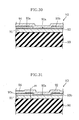
- the thermal printhead X1 includes an insulating substrate 90, a glaze layer 91, a resistor 92, electrodes 93a, 93b, and a protection layer 94 laminated in the mentioned order (see Patent Document 1, for example).
- the resistor 92 includes a heating portion 92a arranged between the electrodes 93a, 93b. The heating portion 92a generates heat which enables printing on a thermal recording medium.
- the electrodes 93a, 93b are formed after the formation of the resistor 92. Formation of the electrodes 93a, 93b is performed by printing and then baking resinate gold paste on the resistor 92. Due to the heat for the baking, the resistor 92 may be oxidized into alteration.
- the resistor 92 and the electrodes 93a, 93b of the thermal printhead X2 shown in Fig. 31 are laminated to each other in an order different from the thermal printhead X1 shown in Fig. 30.
- the resistor 92 is not yet formed.
- the resistor 92 is prevented from being oxidized due to the baking step of the electrodes 93a, 93b.
- thermal printhead X2 shown in Fig. 31 still has room for improvement as described below.
- the electrodes 93a, 93b provide a surface level difference H relative to the glaze layer 91, by the thickness of the electrodes 93a, 93b.
- the resistor 92 is bent through a sharp angle at the portions with the surface level difference H. It is difficult to properly form the resistor 92 with a bend at a sharp angle. Further, the resistor 92 is likely to be disconnected at the bent portions.
- the heating portion 92a of the resistor 92 is arranged at a low portion between the electrodes 93a, 93b.
- a distance between the thermal recording medium and the heating portion 92a is relatively large. This lowers the heat transfer efficiency from the resistor 92a to the thermal recording medium. As a result, the print density is lowered and thus poses difficulty in the high-quality printing as well as the high-speed printing.
- the surface of the protection layer 94 has irregularities because of the arrangement of the electrodes 93a, 93b and the resistor 92. In the irregularities, there is a tendency of accumulation of ink of an ink ribbon for thermal recording or of paper particles of thermal paper. Further, transfer of the thermal recoding medium cannot be performed smoothly in contact with the surface of the protection layer 94.
- Patent Document 1 JP-A-2001-246770
- the present invention is proposed under the above-described circumstances. It is therefore an object of the present invention to provide a thermal printhead and method for manufacturing the same, for preventing disconnection of the resistor, for enhancing heat transfer efficiency from the heating portion of the resistor to the thermal recording medium, and for smooth transfer of the thermal paper.
- a first aspect of the present invention provides a thermal printhead comprising a substrate; a glaze layer formed on the substrate; a plurality of electrodes formed on the glaze layer, the electrodes being spaced from each other; and resistors laminated on the electrodes and the glaze layer, bridging the electrodes.
- the electrodes are embedded in the glaze layer at least at portions laminated with the resistor.
- the electrodes are embedded to a depth causing the surfaces of the electrodes to be flush with the surface of the glaze layer at portions laminated with the resistors.
- the thermalprinthead further comprises a protection layer for covering the electrodes and the resistors.
- each of the electrodes has a melting point higher than softening point of the glaze layer, and is made of a metal having a specific gravity higher than the glaze layer.
- the resistors have a width smaller than a width of the electrode at portions overlapping with the resistors.
- each of the resistor is formed into a strip extending in primary scanning direction.
- the electrodes include a plurality of individual electrodes and at least one common electrode.
- the common electrode includes at least one belt-like portion spaced from the resistor in secondary scanning direction and extending in the primary scanning direction, and also includes a plurality of narrow portions extending from the belt-like portion in the secondary scanning direction across the resistor and being aligned in the secondary scanning direction.
- Each of the individual electrodes includes a narrow portion extending in the secondary scanning direction across the resistor, and is aligned in the primary direction alternately with the narrow portions of the common electrode.
- the common electrode includes a pair of belt-like portions spaced from each other in the secondary scanning direction across the resistor.
- At least one of the narrow portions of the common electrode connect the pair of belt-like portions to each other.
- each of the electrodes is formed with a bonding pad for wire bonding.
- the bonding pad protrudes out of the glaze layer.
- the bonding pad protrudes out of the glaze layer by 1 ⁇ m.
- a portion of the electrodes formed with the bonding pad has a thickness larger than other portion of the electrode without the bonding pad.
- the bonding pad includes a first portion flush with the glaze layer, and a second portion formed on the first portion.
- a second aspect of the present invention provides a method of manufacturing a thermal printhead, comprising the steps of forming a plurality of electrodes spaced from each other on a glaze layer formed on a substrate; and forming a resistor on the glaze layer and the electrodes, the resistor being arranged to bridge the electrodes.
- the method further comprises a step for embedding the electrodes, performed after forming the electrodes and before forming the resistor, in which at least a portion of the glaze layer is softened by heating, so that at least a portion of each of the electrodes is caused to sink into the glaze layer.
- the step for forming the resistor is performed by forming a resistive film and then by performing dry etching at the film.
- the dry etching includes etching by physical energy of ionized gas, and etching by physical energy and chemical action of ionized and activated reactive gas, such as sputter etching, ion beam etching (ion beam sputtering), plasma ashing, plasma etching, and RIE (reactive ion etching).
- the manufacturing method of thermal printhead further comprises a step, performed before the step for embedding the electrodes, for forming a second portion on a part of each of the electrodes.
- the manufacturing method of thermal printhead further comprises a step, performed after the step for embedding the electrodes, for forming a second portion at least partly laminated on a part of each of the electrodes.
- Figs. 1 and 2 illustrate a first embodiment of a thermal printhead according to the present invention.
- the thermal printhead A1 of the embodiment includes a substrate 1, glaze layer 2, a plurality of electrodes 3a-3c, a plurality of resistors 4, and a protection layer 5.
- the protection layer 5 is omitted.
- the substrate 1 is a flat rectangular insulating substrate made of ceramic, and extends in the primary scanning direction y.
- the glaze layer 2 is formed on the substrate 1 by printing and baking an amorphous glass paste, and serves to enhance the heat reservation and to smooth the surface which is to be formed with the plurality of electrodes 3a-3c.
- the glaze layer 2 has a projection 20 having a convex surface. The projection 20 serves to increase the contact pressure between portions of the protection layer 5, corresponding in position to heating portions 40 described below, and a thermal recording medium such as ink ribbon and thermal paper.
- the electrodes 3a-3c are formed on the glaze layer 2 by printing and baking gold resinate paste, for example. As shown in Fig. 2, each of the electrodes 3b is formed in a U-shape with two ends, on the projection 20 of the glaze layer 2, in the vicinity of one side end of the substrate 1.
- each of the electrodes 3a, 3c extends in the secondary scanning direction x.
- One end of the electrode 3a faces and spaced from one end of a respective one of the electrodes 3b.
- the other end of the electrode 3a is connected to a respective one of drive ICs (not shown) for power control.
- One end of the electrode 3c diverges into two legs, each facing and being spaced from the other end of a respective one of the electrode 3b.
- the other end of the electrode 3c is connected to a common line (not shown).
- the electrodes 3a-3c are embedded in the glaze layer 2.
- the surface of the electrodes 3a-3c is substantially flush with the surface of the glaze layer 2.
- a difference in level between the surfaces of the electrodes 3a-3c and the-surface of the glaze layer 2 is completely or almost eliminated.
- the resistors 4 are laminated on the glaze layer 2 and the electrodes 3a-3c, and aligned in the primary scanning direction y, in a manner such that each of the resistor bridges between an end of a respective one of the electrodes 3b and an end of a respective one of the electrodes 3a, 3c.
- the resistor 4 is made of TaSiO 2 , for example.
- the width W4 of the resistor 4 is smaller than the width W3 of the electrodes 3a-3c at portions overlapping with the resistor 4. In the present embodiment, the width W3 is about 25 ⁇ m, while the width W4 is 23 ⁇ m.
- the protection layer 5 is formed to cover the glaze layer 2, the electrodes 3a-3c, and the resistors 4.
- the protection layer 5 is formed by printing and baking glass paste, for example, similarly to the glaze layer 2.
- the protection layer 5 serves to prevent the electrodes 3a-3c and the resistors 4 from directly contacting the thermal recording medium, and from being corroded chemically or electrically.
- the protection layer 5 also serves to enhance the surface smoothness. The smoothed surface reduces friction caused in printing between the protection layer 5 and the thermal recording medium, thereby facilitating the performance of printing.
- each of the resistors 4 is formed without any sharply angled portion, so that disconnection may not occur in the resistor 4.
- the distance between the heating portion 40 and the thermal recording medium is smaller than that of the conventional thermal printheads X1, X2 shown in Figs. 30 and 31. The arrangement improves the heat transfer efficiency between the heating portion 40 and the thermal recording medium, thereby increasing the print density. As a result, high-quality printing and high-speed printing are achieved.
- the resistors 4 and the electrodes 3a-3c may be formed to deviate widthwise from proper positions. If, differing from the present embodiment, the resistors 4 and the electrodes 3a-3c have the same width, overlapping area of each of the resistors 4 and the electrodes 3a-3c is reduced by the size of the deviation. In this case, areas of the resistors 4 heated by electrical current may be irregular in size, and thus printing dots may have variation in size. However, in the present embodiment, the width W4 of the resistors 4 is smaller than the width W3 of the electrodes 3a-3c at portions overlapping with the resistors 4.
- the resistors 4 and the electrodes 3a-3c are formed to deviate widthwise from the proper positions, the resistors 4 can be prevented from unduly protruding out of the electrodes 3a-3c.
- the areas of the resistors 4 overlapping with the electrodes 3a-3c can be a predetermined size, and thus the printing dots can be prevented from having variation in size.
- Figs. 3-11 are plan views and sectional views illustrating a series of steps in the manufacturing method of the thermal printhead A1 according to the present embodiment.
- the substrate 1 is prepared, and the glaze layer 2 is formed on the substrate 1.
- the glaze layer is formed by printing and baking an amorphous glass paste.
- An example of the amorphous glass paste includes a glass material with a glass transition point of 680°C and a softening point of 865°C.
- the upper surface of the glaze layer 2 is formed with the electrodes 3a-3c.
- the electrodes are formed by printing and baking gold resinate paste and then by performing patterning.
- the electrodes 3a-3c are caused to sink into the glaze layer 2.
- the temperature of the glaze layer 2 is heated in a range of the glass transition point to the glass softening point of the glass material, so that the glaze layer 2 is softened.
- the electrodes 3a-3c sink, under their own weight, into the glaze layer 2.
- the depth of this sinking is controllable by adjusting the temperature and time of heating. Specifically, the softening of the glaze layer 2 is finished on or right before the moment when the surfaces of the electrodes 3a-3c come to be flush with the surface of the glaze layer 2.
- the resistors 4 are formed.
- a resistor film 4A is formed to cover the electrodes 3a-3c.
- the resistor film 4A is made of TaSiO 2 , for example, and may be a thick film or a thin film.
- a plurality of resistors 4 are formed to bridge between the ends of the electrodes 3b and the ends of the electrodes 3a, 3c.
- the width W4 is formed to be smaller than the width W3 of the electrodes 3a-3c at portions overlapping with the resistors 4.
- the protection layer 5 is formed to cover the electrodes 3a-3c and the resistors 4 by performing thick-film printing and baking glass paste. Alternatively, sputtering with SiO 2 , SiAlON may be performed to form the protection layer 5. Through these steps, the thermal printhead A1 shown in Figs. 1 and 2 is made.
- the glaze layer 2 is softened, so that the electrodes 3a-3c sink under their own weight.
- This method is easier than the method in which the glaze layer 2 is partly cut to form the electrodes 3a-3c therein.
- sinking depth of the electrodes 3a-3c into the glaze layer 2 can be adjusted.
- improper gap can be prevented from being formed between the glaze layer 2 and the electrodes 3a-3c.
- gold is used as a material of electrodes 3a-3c.
- Gold has relatively high melting point, and has corrosion resistance higher than that of e.g. aluminum. Further, specific gravity of gold is greater than that of material of the glaze layer. Therefore, in softening the glaze layer 2 by heating, the electrodes are prevented from oxidation and quickly sink into the glaze layer 2 under gravity.
- the resistors 4 can be accurately formed in a predetermined size.
- the difference between these widths need not to be excessively large.
- widthwise deviation may occur while the electrodes 3a-3c sink into the glaze layer.
- the difference between the widths W3, W4 may be the same as or measurably larger than the deviation. In this way, printing dots can be properly prevented from having variation in size due to such deviation.
- Figs. 12-29 illustrate other examples of the thermal printhead and manufacturing method according to the present invention.
- elements identical or similar to those in the above first embodiment are indicated by the same reference numbers and duplicated description will be omitted.
- Figs. 12-14 illustrate a thermal printhead according to a second embodiment.of the present invention.
- the thermal printhead A2 of the present embodiment differs from the above first embodiment in arrangement of the electrodes and in the form of the resistor 4.
- the protection layer 5 is omitted in Fig. 12.
- a plurality of individual electrodes 3d are aligned in the primary scanning direction y.
- Each of the individual electrodes 3d includes a narrow portion 31 and a bonding pad 32.
- the narrow portion 31 is elongated in the secondary scanning direction x and lies between the resistor 4 and the glaze layer 2.
- the bonding pad 32 is a portion for bonding a wire W, and includes a first portion 32a and an second portion 32b.
- the first portion 32a connected to the narrow portion 31 is made by printing and baking gold resinate paste.
- Each of the narrow portion 31 and the first portion 32a has a thickness of 0.6 ⁇ m and an upper surface substantially flush with the glaze layer 2.
- the second portion 32b protrudes upwardly from the glaze layer 2, and the wire W is directly bonded thereto.
- the second portion 32b is made by printing and baking gold paste, and has a thickness of 1 ⁇ m.
- the gold paste is a paste, different from gold resinate paste, in which gold particles are mixed with a binder.
- a film formed of gold resinate paste has a relatively small thickness which is suitable for forming a smooth surface, while a film formed of the gold paste has a relatively large thickness.
- sputtering of gold may be performed to make the second portion 32b.
- the common electrode 3e includes a pair of belt-like portions 35, 36 and a plurality of narrow portions 37.
- the belt-like portions 35, 36 are elongated in the primary scanning direction y, and spaced from each other in the secondary scanning direction x across the resistor 4.
- the narrow portions 37 are elongated in the secondary scanning direction x, and are aligned in the primary scanning direction alternately with the individual electrodes 3d.
- the belt-like portions 35, 36 are connected to each other via the narrow portions 37.
- the belt-like portion 35 partly serves as a bonding pad for bonding the wire W.
- the belt-like portion 35 includes a first portion 35a and a second portion 35b.
- the first portion 35a is connected to the narrow portions 37 and to the belt-like portion 36, and is made by printing and baking gold resinate paste.
- Each of the first portion 35a, the narrow portions 37, and the belt-like portion 36 has a thickness of 0.6 ⁇ m and an upper surface substantially flush with the glaze layer 2.
- the second portion 35b is made, similarly to the second portions 32, by printing and baking gold paste, and has a thick ness of 1 ⁇ m.
- the resistor 4 is, as shown in Fig. 12, formed in a strip elongated in the primary scanning direction y, and as shown in Fig. 13, arranged above the projection 20 of the glaze layer 2. As shown in Figs. 12 and 14, the resistor 4 is laminated on the narrow portions 31 of the individual electrodes 3d and the narrow portions 37 of the common electrode 3e. The resistor 4 serves as the heating portions 40 at portions between the narrow portions 31 and the narrow portions 37. As shown in Fig. 14, the narrow portions 31, the narrow portions 37, and the glaze layer 2 are flush with each other, so that the resistor 4 has a smooth surface extending in the primary scanning direction y, with little difference in level.
- non-illustrated drive ICs select one of the individual electrodes 3d.
- an electrical current flows between the selected individual electrodes 3d and the narrow portions 37, thereby generating heat at the heating portions 40.
- the heat is transmitted to a thermal recording medium for performing printing thereon.
- the thermal printhead A2 is able to perform clear printing.
- the thermal printhead is especially suitable to be used in a high-definition printer, for performing clear printing at downsized printing dots.
- Energizing of the heating portion 40 is performed through the belt-like portions 35, 36.
- the total area of the belt-like portions 35, 36 is relatively large, which prevents voltage reduction at the belt-like portions 35, 36.
- the width of the belt-like portion 36 can be relatively small.
- the resistor 4 can be arranged close to the right end of the substrate 1. In this way, the thermal printhead A2 can be designed as so-called near-edge type, in which the resistor 4 is arranged in the vicinity of the right end of the substrate 1.
- Each of the bonding pads 32 and the belt-like portion 35 has a relatively large thickness of about 1.6 ⁇ m. Therefore, bonding strength of the wire W can be increased.
- Figs 15-23 are plan views and sectional views illustrating a series of steps in the manufacturing method of the thermal printhead A2 according to the present embodiment.
- the substrate 1 is prepared, and the glaze layer 2 is formed on the substrate 1.
- the glaze layer 2 is formed by performing thick-filmprinting and baking, using an amorphous glass paste.
- a thin gold layer 3A is formed.
- the thin gold layer 3A is formed by printing and baking gold resinate paste.
- the thickness of the thin gold layer 3A is about 0.6 ⁇ m.
- a thin gold layer 3B is formed on the thin gold layer 3A.
- the thickness of the thin gold layer 3B is about 1 ⁇ m.
- the right side portion of the thin gold layer 3A is exposed from the thin gold layer 3B.
- the thin gold layer 3B is formed by printing and baking gold paste. Differently from the present embodiment, the thin gold layer 3B may be formed, by repeating the printing and baking of gold resinate paste.
- the thin gold layer 3B may also be formed by sputtering gold.
- patterning is performed at the gold thin layers 3A, 3B, so that the individual electrodes 3d and the common electrode 3e are formed as shown in Figs. 19 and 20.
- the patterning is performed by wet etching, for example.
- the individual electrodes 3d and the common electrode 3e are caused to sink into the glaze layer 2.
- This step for sinking the electrodes is performed similarly to the method described with reference to Fig. 7.
- the upper surfaces of the narrow portions 31, the narrow portions 37, and the belt-like portion 36 are arranged to be flush with the surface of the glaze layer 2.
- the second portions 32b, 35b of the bonding pads 32 and the belt-like portion 35 protrude from the glaze layer 2.
- a resistor film 4A is formed. Then, patterning is performed at the resistor film 4A to form the resistor 4, as shown in Fig. 23. Subsequently, the protection layer 5 is formed to cover the resistor 4, the belt-like portion 36, a part of each of the narrow portions 31, and a part of each of the narrow portions 37. After performing other steps such as bonding the wire W at each of the bonding pads 32 and the belt-like portion 35, the thermal printhead A2 shown in Figs. 12-14 is obtained.
- Figs. 24 and 25 illustrate a thermal printhead according a third embodiment of the present invention.
- the thermal printhead A3 differs from the second embodiment in structure of the bonding pads 32 and in form of the common electrode 3e.
- the protection layer 5 is omitted in Fig. 24.
- each of the bonding pads 32 includes a first portion 32a partly overlapping with a second portion 32b.
- the bonding pad is identical to the second embodiment in that the first portion 32a has an upper surface flush with the surface of the glaze layer 2, and the second portion 32b protrudes out of the glaze layer 2.
- the common electrode 3e includes one belt-like portion 36.
- the wire W can be properly bonded, and the bonding strength between the wire W and the bonding pad 32 can be increased. Further, as the area of the first portion 32a is reduced, gold material can be saved.
- Figs. 26-29 are sectional views illustrating a series of steps in the manufacturing method of the thermal printhead A3 according to the present embodiment.
- the substrate 1 is first formed with a glaze layer 2 and a gold thin layer 3A. Then, patterning is performed at the gold thin layer 3A to form electrodes 3Ad and a common electrode 3e.
- the electrodes 3Ad and the common electrode 3e are caused to sink into the glaze layer 2.
- the upper surfaces of the electrodes 3Ad come to be flush with the surface of the glaze layer 2.
- a gold thin layer 3B is formed.
- the gold thin layer 3B is formed by printing and baking gold paste.
- the gold thin layer 3B has a thickness of about 1 ⁇ m.
- the gold thin layer 3B partly overlaps with the first portions 32a at its right side end.
- patterning is performed at the gold thin layer 3B to form the secondportions 32b shown in Fig. 29. In this way, the individual electrodes 3d are made. Thereafter, the same steps as the second embodiment are performed to obtain the thermal printhead A3.
- the step for sinking the electrodes is performed before forming the second portions 32b on the first portions 32a and the glaze layer 2.
- the bonding pads 32 can reliably protrude out of the glaze layer 2 by the thickness of the gold thin layer 3B or the second portions 32b. This is suitable to perform the wire bonding properly.
- the electrodes 3a-3c are arranged to sink into the glaze layer so that the electrodes 3a-3c come to be substantially flush with the glaze layer 2, though not limited to this.
- the electrodes 3a-3c may be partly embedded in the glaze layer 2 at their bottom portions, and the other portions may protrude above the glaze layer 2. Even with such structure, the difference in level between the electrodes 3a-3c and the glaze layer 2 can be reduced, thereby obtaining an effect in comparison with the conventional arrangement.
- each of the electrodes 3a-3c is arranged to be embedded in the glaze layer 2, though not limited to this. It suffices if each of the electrodes 3a-3c is sunk at least at a portion laminated with the resistor 4.
- the method for sinking the electrodes 3a-3c into the glaze layer 2 is not limited to the present embodiments, but a portion of the glaze layer to be formed with the electrodes may be curved to form recesses, corresponding to the thickness of the electrodes, and the electrodes may formed in the recess by thick-film printing.
- the gold thin layers 3A, 3B are laminated to each other, however, the gold thin layer 3A may be formed to have a thickness of about 1.6 ⁇ m, and etching may be performed at the thin layer 3A several times, so that the thickness of the bonding pad 32 is larger than the other portion of the individual electrode 3d. Similar method may be utilized to form the common electrode 3e.
Landscapes
- Electronic Switches (AREA)
Abstract
A thermal printhead (A1) includes electrodes (3a-3c) embedded in a glaze layer 2 at least at a portion laminated with a resistor (4). Favorably, the portion of the electrodes (3a-3c) laminated with the resistor (4) is sunk to a depth causing the surfaces of the electrodes to be flush with the surface of the glaze layer 2. Such structure enhances the heat transfer efficiency from a heating portion (40) of the resistor (4) to a thermal recording medium, and smooth transfer of thermal recording paper.
Description
- The present invention relates to a thermal-printhead and method for manufacturing the same.
- Figs. 30 and 31 illustrate conventional thermal printheads. The thermal printhead X1 includes an
insulating substrate 90, aglaze layer 91, aresistor 92,electrodes protection layer 94 laminated in the mentioned order (seePatent Document 1, for example). Theresistor 92 includes aheating portion 92a arranged between theelectrodes heating portion 92a generates heat which enables printing on a thermal recording medium. - In manufacturing the thermal printhead X1, the
electrodes resistor 92. Formation of theelectrodes resistor 92. Due to the heat for the baking, theresistor 92 may be oxidized into alteration. - To solve this problem, the
resistor 92 and theelectrodes electrodes resistor 92 is not yet formed. Thus, theresistor 92 is prevented from being oxidized due to the baking step of theelectrodes - However, the thermal printhead X2 shown in Fig. 31 still has room for improvement as described below.
- First, the
electrodes glaze layer 91, by the thickness of theelectrodes resistor 92 is bent through a sharp angle at the portions with the surface level difference H. It is difficult to properly form theresistor 92 with a bend at a sharp angle. Further, theresistor 92 is likely to be disconnected at the bent portions. - Second, the
heating portion 92a of theresistor 92 is arranged at a low portion between theelectrodes heating portion 92a is relatively large. This lowers the heat transfer efficiency from theresistor 92a to the thermal recording medium. As a result, the print density is lowered and thus poses difficulty in the high-quality printing as well as the high-speed printing. - Third, the surface of the
protection layer 94 has irregularities because of the arrangement of theelectrodes resistor 92. In the irregularities, there is a tendency of accumulation of ink of an ink ribbon for thermal recording or of paper particles of thermal paper. Further, transfer of the thermal recoding medium cannot be performed smoothly in contact with the surface of theprotection layer 94.
Patent Document 1:JP-A-2001-246770 - The present invention is proposed under the above-described circumstances. It is therefore an object of the present invention to provide a thermal printhead and method for manufacturing the same, for preventing disconnection of the resistor, for enhancing heat transfer efficiency from the heating portion of the resistor to the thermal recording medium, and for smooth transfer of the thermal paper.
- A first aspect of the present invention provides a thermal printhead comprising a substrate; a glaze layer formed on the substrate; a plurality of electrodes formed on the glaze layer, the electrodes being spaced from each other; and resistors laminated on the electrodes and the glaze layer, bridging the electrodes. The electrodes are embedded in the glaze layer at least at portions laminated with the resistor.
- Favorably, the electrodes are embedded to a depth causing the surfaces of the electrodes to be flush with the surface of the glaze layer at portions laminated with the resistors.
- Favorably, the thermalprinthead further comprises a protection layer for covering the electrodes and the resistors.
- Favorably, each of the electrodes has a melting point higher than softening point of the glaze layer, and is made of a metal having a specific gravity higher than the glaze layer.
- Favorably, the resistors have a width smaller than a width of the electrode at portions overlapping with the resistors.
- Favorably, each of the resistor is formed into a strip extending in primary scanning direction. The electrodes include a plurality of individual electrodes and at least one common electrode. The common electrode includes at least one belt-like portion spaced from the resistor in secondary scanning direction and extending in the primary scanning direction, and also includes a plurality of narrow portions extending from the belt-like portion in the secondary scanning direction across the resistor and being aligned in the secondary scanning direction. Each of the individual electrodes includes a narrow portion extending in the secondary scanning direction across the resistor, and is aligned in the primary direction alternately with the narrow portions of the common electrode.
- Favorably, the common electrode includes a pair of belt-like portions spaced from each other in the secondary scanning direction across the resistor.
- Favorably, at least one of the narrow portions of the common electrode connect the pair of belt-like portions to each other.
- Favorably, each of the electrodes is formed with a bonding pad for wire bonding. The bonding pad protrudes out of the glaze layer.
- Favorably, the bonding pad protrudes out of the glaze layer by 1µm.
- Favorably, a portion of the electrodes formed with the bonding pad has a thickness larger than other portion of the electrode without the bonding pad.
- Favorably, the bonding pad includes a first portion flush with the glaze layer, and a second portion formed on the first portion.
- A second aspect of the present invention provides a method of manufacturing a thermal printhead, comprising the steps of forming a plurality of electrodes spaced from each other on a glaze layer formed on a substrate; and forming a resistor on the glaze layer and the electrodes, the resistor being arranged to bridge the electrodes. The method further comprises a step for embedding the electrodes, performed after forming the electrodes and before forming the resistor, in which at least a portion of the glaze layer is softened by heating, so that at least a portion of each of the electrodes is caused to sink into the glaze layer.
- Favorably, the step for forming the resistor is performed by forming a resistive film and then by performing dry etching at the film. Here, the dry etching includes etching by physical energy of ionized gas, and etching by physical energy and chemical action of ionized and activated reactive gas, such as sputter etching, ion beam etching (ion beam sputtering), plasma ashing, plasma etching, and RIE (reactive ion etching).
- Favorably, the manufacturing method of thermal printhead further comprises a step, performed before the step for embedding the electrodes, for forming a second portion on a part of each of the electrodes.
- Favorably, the manufacturing method of thermal printhead further comprises a step, performed after the step for embedding the electrodes, for forming a second portion at least partly laminated on a part of each of the electrodes.
- Other advantages and features will be apparent from the following description of the embodiments.
-
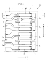
- Fig. 1 is a plan view illustrating the principal portions of a thermal printhead according to a first embodiment of the present invention.
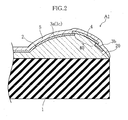
- Fig. 2 is a sectional view taken along the lines II-II of Fig. 1.
- Fig. 3 is a plan view illustrating a step for forming a glaze layer in an example of manufacturing method of the thermal printhead shown in Figs. 1 and 2.
- Fig. 4 is a sectional view taken along lines IV-IV of Fig. 3.
- Fig. 5 is a plan view illustrating a step for forming electrodes in the example of manufacturing method of the thermal printhead shown in Figs. 1 and 2.
- Fig. 6 is a sectional view taken along lines VI-VI of Fig. 5.
- Fig. 7 is a sectional view illustrating a step for embedding electrodes in the example of manufacturing method of the thermal printhead shown in Figs. 1 and 2.
- Fig. 8 is a plan view illustrating a step for forming a resistive film in the example of manufacturing method of the thermal printhead shown in Figs. 1 and 2.
- Fig. 9 is a sectional view taken along lines IX-IX in Fig. 8.
- Fig. 10 is a plan view illustrating a step for forming resistors in the example of manufacturing method of the thermal printhead shown in Figs. 1 and 2.
- Fig. 11 is a sectional view taken along lines XI-XI in Fig. 10.
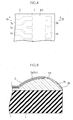
- Fig. 12 is a plan view illustrating a thermal printhead according to a second embodiment of the present invention.
- Fig. 13 is a sectional view taken along lines XIII-XIII of Fig. 12.
- Fig. 14 is a sectional view taken along lines XIV-XIV of Fig. 12.
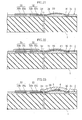
- Fig. 15 is a sectional view illustrating a step for forming a glaze layer in an example of manufacturing method of the thermal printhead shown in Figs. 12-14.
- Fig. 16 is a sectional view illustrating a step for forming a gold thin layer in the example of manufacturing method of the thermal printhead shown in Figs. 12-14.
- Fig. 17 is a plan view illustrating a step for forming another gold thin layer in the example of manufacturing method of the thermal printhead shown in Figs. 12-14.
- Fig. 18 is a sectional view taken along lines XVIII-XVIII of Fig. 17.
- Fig. 19 is a plan view illustrating a step for forming electrodes in the example of manufacturing method of the thermal printhead shown in Figs. 12-14.
- Fig. 20 is a sectional view taken along lines XX-XX of Fig. 19.
- Fig. 21 is a sectional view illustrating a step for embedding the electrodes in the example ofmanufacturingmethod of the thermal printhead shown in Figs. 12-14.
- Fig. 22 is a sectional view illustrating a step for forming a resistive film in the example of manufacturing method of the thermal printhead shown in Figs. 12-14.
- Fig. 23 is a sectional view illustrating a step for forming a resistor and a protection layer in the example of manufacturing method of the thermal printhead shown in Figs. 12-14.
- Fig. 24 is a plan view illustrating a thermal printhead according to a third embodiment of the present invention.
- Fig. 25 is a sectional view taken along lines XXV-XXV of Fig. 24.
- Fig. 26 is a sectional view illustrating a step for forming an electrode in an example of manufacturing method of the thermal printhead shown in Figs. 24 and 25.
- Fig. 27 is a sectional view illustrating a step for embedding the electrode in the example of manufacturing method of the thermal printhead shown in Figs. 24 and 25.
- Fig. 28 is a sectional view illustrating a step for forming a gold thin layer in the example of manufacturing method of the thermal print head shown in Figs. 24 and 25.
- Fig. 29 is a sectional view illustrating a step for forming another electrode in the example of manufacturing method of the thermal printhead shown in Figs. 24 and 25.
- Fig. 30 is a sectional view illustrating an example of a conventional thermal printhead.
- Fig. 31 is a sectional view illustrating another example of a conventional thermal printhead.
- A preferred embodiment of the present invention is specifically described below with reference to the accompanying drawings.
- Figs. 1 and 2 illustrate a first embodiment of a thermal printhead according to the present invention. The thermal printhead A1 of the embodiment includes a
substrate 1,glaze layer 2, a plurality ofelectrodes 3a-3c, a plurality ofresistors 4, and aprotection layer 5. In Fig. 1, theprotection layer 5 is omitted. - The
substrate 1 is a flat rectangular insulating substrate made of ceramic, and extends in the primary scanning direction y. Theglaze layer 2 is formed on thesubstrate 1 by printing and baking an amorphous glass paste, and serves to enhance the heat reservation and to smooth the surface which is to be formed with the plurality ofelectrodes 3a-3c. Theglaze layer 2 has aprojection 20 having a convex surface. Theprojection 20 serves to increase the contact pressure between portions of theprotection layer 5, corresponding in position toheating portions 40 described below, and a thermal recording medium such as ink ribbon and thermal paper. - The
electrodes 3a-3c are formed on theglaze layer 2 by printing and baking gold resinate paste, for example. As shown in Fig. 2, each of theelectrodes 3b is formed in a U-shape with two ends, on theprojection 20 of theglaze layer 2, in the vicinity of one side end of thesubstrate 1. - As shown in Fig. 1, each of the
electrodes electrode 3a faces and spaced from one end of a respective one of theelectrodes 3b. The other end of theelectrode 3a is connected to a respective one of drive ICs (not shown) for power control. One end of theelectrode 3c diverges into two legs, each facing and being spaced from the other end of a respective one of theelectrode 3b. The other end of theelectrode 3c is connected to a common line (not shown). When the drive ICs are switched on, an electrical current flows from the common line to theresistor 4 and theelectrodes electrode 3c. - As shown in Fig. 2, the
electrodes 3a-3c are embedded in theglaze layer 2. Thus, the surface of theelectrodes 3a-3c is substantially flush with the surface of theglaze layer 2. In other words, a difference in level between the surfaces of theelectrodes 3a-3c and the-surface of theglaze layer 2 is completely or almost eliminated. - The
resistors 4 are laminated on theglaze layer 2 and theelectrodes 3a-3c, and aligned in the primary scanning direction y, in a manner such that each of the resistor bridges between an end of a respective one of theelectrodes 3b and an end of a respective one of theelectrodes resistor 4 is made of TaSiO2, for example. The width W4 of theresistor 4 is smaller than the width W3 of theelectrodes 3a-3c at portions overlapping with theresistor 4. In the present embodiment, the width W3 is about 25µm, while the width W4 is 23µm. - The
protection layer 5 is formed to cover theglaze layer 2, theelectrodes 3a-3c, and theresistors 4. Theprotection layer 5 is formed by printing and baking glass paste, for example, similarly to theglaze layer 2. Theprotection layer 5 serves to prevent theelectrodes 3a-3c and theresistors 4 from directly contacting the thermal recording medium, and from being corroded chemically or electrically. Theprotection layer 5 also serves to enhance the surface smoothness. The smoothed surface reduces friction caused in printing between theprotection layer 5 and the thermal recording medium, thereby facilitating the performance of printing. - Next, the function of the thermal printhead A1 is described below.
- In the thermal printhead A1 of the present embodiment, a difference in level between the surface of the
glaze layer 2 and the surface of theelectrodes 3a-3c is completely or almost eliminated. Thus, each of theresistors 4 is formed without any sharply angled portion, so that disconnection may not occur in theresistor 4. Further, as theheating portion 40 of theresistor 4 is not embedded deep between theelectrodes electrodes 3b, the distance between theheating portion 40 and the thermal recording medium is smaller than that of the conventional thermal printheads X1, X2 shown in Figs. 30 and 31. The arrangement improves the heat transfer efficiency between theheating portion 40 and the thermal recording medium, thereby increasing the print density. As a result, high-quality printing and high-speed printing are achieved. Still further, a difference in level on the surface of theprotection layer 5 covering theglaze layer 2 and theelectrodes 3a-3c is reduced. This prevents accumulation of ink of an ink ribbon, for example, in irregularities on the surface of theprotection layer 5. It also enables thermal paper as the thermal recording medium to be smoothly transferred while contacting the surface of theprotection layer 5. - In manufacturing the thermal printhead A1, the
resistors 4 and theelectrodes 3a-3c may be formed to deviate widthwise from proper positions. If, differing from the present embodiment, theresistors 4 and theelectrodes 3a-3c have the same width, overlapping area of each of theresistors 4 and theelectrodes 3a-3c is reduced by the size of the deviation. In this case, areas of theresistors 4 heated by electrical current may be irregular in size, and thus printing dots may have variation in size. However, in the present embodiment, the width W4 of theresistors 4 is smaller than the width W3 of theelectrodes 3a-3c at portions overlapping with theresistors 4. Thus, even if theresistors 4 and theelectrodes 3a-3c are formed to deviate widthwise from the proper positions, theresistors 4 can be prevented from unduly protruding out of theelectrodes 3a-3c. In this way, the areas of theresistors 4 overlapping with theelectrodes 3a-3c can be a predetermined size, and thus the printing dots can be prevented from having variation in size. - Next, an example of manufacturing method of the thermal printhead A1 is described with reference to Figs. 3-11. Figs. 3-11 are plan views and sectional views illustrating a series of steps in the manufacturing method of the thermal printhead A1 according to the present embodiment.
- First, as shown in Figs. 3 and 4, the
substrate 1 is prepared, and theglaze layer 2 is formed on thesubstrate 1. The glaze layer is formed by printing and baking an amorphous glass paste. An example of the amorphous glass paste includes a glass material with a glass transition point of 680°C and a softening point of 865°C. - Next, as shown in Figs. 5 and 6, the upper surface of the
glaze layer 2 is formed with theelectrodes 3a-3c. The electrodes are formed by printing and baking gold resinate paste and then by performing patterning. - After forming the
electrodes 3a-3c, as shown in Fig. 7, theelectrodes 3a-3c are caused to sink into theglaze layer 2. In this step, the temperature of theglaze layer 2 is heated in a range of the glass transition point to the glass softening point of the glass material, so that theglaze layer 2 is softened. When theglaze layer 2 is softened, theelectrodes 3a-3c sink, under their own weight, into theglaze layer 2. The depth of this sinking is controllable by adjusting the temperature and time of heating. Specifically, the softening of theglaze layer 2 is finished on or right before the moment when the surfaces of theelectrodes 3a-3c come to be flush with the surface of theglaze layer 2. - After the
electrodes 3a-3c are sunk, theresistors 4 are formed. In forming theresistors 4, as shown in Figs. 8 and 9, aresistor film 4A is formed to cover theelectrodes 3a-3c. Theresistor film 4A is made of TaSiO2, for example, and may be a thick film or a thin film. Next, by performing dry etching at theresistor film 4A, and as shown in Figs. 10 and 11, a plurality ofresistors 4 are formed to bridge between the ends of theelectrodes 3b and the ends of theelectrodes electrodes 3a-3c at portions overlapping with theresistors 4. - Finally, the
protection layer 5 is formed to cover theelectrodes 3a-3c and theresistors 4 by performing thick-film printing and baking glass paste. Alternatively, sputtering with SiO2, SiAlON may be performed to form theprotection layer 5. Through these steps, the thermal printhead A1 shown in Figs. 1 and 2 is made. - In the manufacturing method of the thermal printhead A1 according to the present embodiment, for sinking the
electrodes 3a-3c into theglaze layer 2, theglaze layer 2 is softened, so that theelectrodes 3a-3c sink under their own weight. This method is easier than the method in which theglaze layer 2 is partly cut to form theelectrodes 3a-3c therein. By controlling the temperature and time for heating theglaze layer 2, sinking depth of theelectrodes 3a-3c into theglaze layer 2 can be adjusted. In addition, improper gap can be prevented from being formed between theglaze layer 2 and theelectrodes 3a-3c. - In the above-described manufacturing method, gold is used as a material of
electrodes 3a-3c. Gold has relatively high melting point, and has corrosion resistance higher than that of e.g. aluminum. Further, specific gravity of gold is greater than that of material of the glaze layer. Therefore, in softening theglaze layer 2 by heating, the electrodes are prevented from oxidation and quickly sink into theglaze layer 2 under gravity. - Further, by forming the
resistors 4 in dry etching, theresistors 4 can be accurately formed in a predetermined size. Thus, in forming theresistors 4 with the width W4 smaller than the width W3 of theelectrodes 3a-3c at portions overlapping with theresistors 4, the difference between these widths need not to be excessively large. Specifically, in the step for embedding theelectrodes 3a-3c, widthwise deviation may occur while theelectrodes 3a-3c sink into the glaze layer. Here, the difference between the widths W3, W4 may be the same as or measurably larger than the deviation. In this way, printing dots can be properly prevented from having variation in size due to such deviation. - Figs. 12-29 illustrate other examples of the thermal printhead and manufacturing method according to the present invention. In the figures, elements identical or similar to those in the above first embodiment are indicated by the same reference numbers and duplicated description will be omitted.
- Figs. 12-14 illustrate a thermal printhead according to a second embodiment.of the present invention. The thermal printhead A2 of the present embodiment differs from the above first embodiment in arrangement of the electrodes and in the form of the
resistor 4. Theprotection layer 5 is omitted in Fig. 12. - As shown in Fig. 12, a plurality of
individual electrodes 3d are aligned in the primary scanning direction y. Each of theindividual electrodes 3d includes anarrow portion 31 and abonding pad 32. - The
narrow portion 31 is elongated in the secondary scanning direction x and lies between theresistor 4 and theglaze layer 2. Thebonding pad 32 is a portion for bonding a wire W, and includes afirst portion 32a and ansecond portion 32b. Thefirst portion 32a connected to thenarrow portion 31 is made by printing and baking gold resinate paste. Each of thenarrow portion 31 and thefirst portion 32a has a thickness of 0.6µm and an upper surface substantially flush with theglaze layer 2. Thesecond portion 32b protrudes upwardly from theglaze layer 2, and the wire W is directly bonded thereto. - The
second portion 32b is made by printing and baking gold paste, and has a thickness of 1µm. Here, the gold paste is a paste, different from gold resinate paste, in which gold particles are mixed with a binder. A film formed of gold resinate paste has a relatively small thickness which is suitable for forming a smooth surface, while a film formed of the gold paste has a relatively large thickness. In place of printing and baking the gold paste, sputtering of gold may be performed to make thesecond portion 32b. - As shown in Fig. 12, the
common electrode 3e includes a pair of belt-like portions narrow portions 37. The belt-like portions resistor 4. Thenarrow portions 37 are elongated in the secondary scanning direction x, and are aligned in the primary scanning direction alternately with theindividual electrodes 3d. The belt-like portions narrow portions 37. - The belt-
like portion 35 partly serves as a bonding pad for bonding the wire W. As shown in Fig. 13, the belt-like portion 35 includes afirst portion 35a and asecond portion 35b. Thefirst portion 35a is connected to thenarrow portions 37 and to the belt-like portion 36, and is made by printing and baking gold resinate paste. Each of thefirst portion 35a, thenarrow portions 37, and the belt-like portion 36 has a thickness of 0.6µm and an upper surface substantially flush with theglaze layer 2. Thesecond portion 35b is made, similarly to thesecond portions 32, by printing and baking gold paste, and has a thick ness of 1µm. - The
resistor 4 is, as shown in Fig. 12, formed in a strip elongated in the primary scanning direction y, and as shown in Fig. 13, arranged above theprojection 20 of theglaze layer 2. As shown in Figs. 12 and 14, theresistor 4 is laminated on thenarrow portions 31 of theindividual electrodes 3d and thenarrow portions 37 of thecommon electrode 3e. Theresistor 4 serves as theheating portions 40 at portions between thenarrow portions 31 and thenarrow portions 37. As shown in Fig. 14, thenarrow portions 31, thenarrow portions 37, and theglaze layer 2 are flush with each other, so that theresistor 4 has a smooth surface extending in the primary scanning direction y, with little difference in level. - In printing by the thermal printhead A2, non-illustrated drive ICs select one of the
individual electrodes 3d. Here, an electrical current flows between the selectedindividual electrodes 3d and thenarrow portions 37, thereby generating heat at theheating portions 40. The heat is transmitted to a thermal recording medium for performing printing thereon. - Next, the function of the thermal printheadA2 is described below.
- In the present embodiment, as shown, in Fig. 14, as the
resistor 4 has a smooth surface extending in the primary scanning direction y, a portion of theprotection layer 5 covering theresistor 4 also has a smooth surface extending in the primary scanning direction y. Thus, the portion of theprotection layer 5 covering theresistor 4 is suitable for sticking to the thermal recording medium. Even if the thermal recording medium is made of a relatively hard material such as plastic, theprotection layer 5 can properly stick to the thermal recording medium. This facilitates the heat transmission from theheating portions 40 of theresistor 4 to the thermal recording medium. Therefore, the thermal printhead A2 is able to perform clear printing. The thermal printhead is especially suitable to be used in a high-definition printer, for performing clear printing at downsized printing dots. - Energizing of the
heating portion 40 is performed through the belt-like portions like portions like portions like portion 36 can be relatively small. When the belt-like portion 36 has a small width, theresistor 4 can be arranged close to the right end of thesubstrate 1. In this way, the thermal printhead A2 can be designed as so-called near-edge type, in which theresistor 4 is arranged in the vicinity of the right end of thesubstrate 1. - Each of the
bonding pads 32 and the belt-like portion 35, to which the wire W is bonded, protrudes from theglaze layer 2. Thus, even if a tip of a bonding tool for bonding the wire W is larger than e.g. thebonding pad 32, the bonding tool is prevented from unduly contacting theglaze layer 2. Therefore, the wire W can be properly bonded. Each of thebonding pads 32 and the belt-like portion 35 has a relatively large thickness of about 1.6µm. Therefore, bonding strength of the wire W can be increased. - Next, an example of manufacture method of the thermal printhead A2 is described below with reference to Figs. 15-23. Figs 15-23 are plan views and sectional views illustrating a series of steps in the manufacturing method of the thermal printhead A2 according to the present embodiment.
- First, as shown in Fig. 15, the
substrate 1 is prepared, and theglaze layer 2 is formed on thesubstrate 1. Theglaze layer 2 is formed by performing thick-filmprinting and baking, using an amorphous glass paste. - Next, as shown in Fig. 16, a
thin gold layer 3A is formed. Thethin gold layer 3A is formed by printing and baking gold resinate paste. Here, the thickness of thethin gold layer 3A is about 0.6µm. - Subsequently, as shown in Figs. 17 and 18, a
thin gold layer 3B is formed on thethin gold layer 3A. Here, the thickness of thethin gold layer 3B is about 1µm. The right side portion of thethin gold layer 3A is exposed from thethin gold layer 3B. Thethin gold layer 3B is formed by printing and baking gold paste. Differently from the present embodiment, thethin gold layer 3B may be formed, by repeating the printing and baking of gold resinate paste. Thethin gold layer 3B may also be formed by sputtering gold. - After forming the gold
thin layers thin layers individual electrodes 3d and thecommon electrode 3e are formed as shown in Figs. 19 and 20. The patterning is performed by wet etching, for example. - Next, as shown in Fig. 21, the
individual electrodes 3d and thecommon electrode 3e are caused to sink into theglaze layer 2. This step for sinking the electrodes is performed similarly to the method described with reference to Fig. 7. In this step, the upper surfaces of thenarrow portions 31, thenarrow portions 37, and the belt-like portion 36 are arranged to be flush with the surface of theglaze layer 2. Thesecond portions bonding pads 32 and the belt-like portion 35 protrude from theglaze layer 2. - After the electrodes are sunk, as shown in Fig. 22, a
resistor film 4A is formed. Then, patterning is performed at theresistor film 4A to form theresistor 4, as shown in Fig. 23. Subsequently, theprotection layer 5 is formed to cover theresistor 4, the belt-like portion 36, a part of each of thenarrow portions 31, and a part of each of thenarrow portions 37. After performing other steps such as bonding the wire W at each of thebonding pads 32 and the belt-like portion 35, the thermal printhead A2 shown in Figs. 12-14 is obtained. - According to the manufacturing method, only the
bonding pads 32 and the belt-like portion 35 of theindividual electrodes 3d and thecommon electrode 3e protrude from theglaze layer 2 by a desired height. This facilitates bonding of the wire W. - Figs. 24 and 25 illustrate a thermal printhead according a third embodiment of the present invention. The thermal printhead A3 differs from the second embodiment in structure of the
bonding pads 32 and in form of thecommon electrode 3e. Theprotection layer 5 is omitted in Fig. 24. - As shown in Fig. 25, each of the
bonding pads 32 includes afirst portion 32a partly overlapping with asecond portion 32b. The bonding pad is identical to the second embodiment in that thefirst portion 32a has an upper surface flush with the surface of theglaze layer 2, and thesecond portion 32b protrudes out of theglaze layer 2. Thecommon electrode 3e includes one belt-like portion 36. - With such structure, the wire W can be properly bonded, and the bonding strength between the wire W and the
bonding pad 32 can be increased. Further, as the area of thefirst portion 32a is reduced, gold material can be saved. - Next, an example of manufacturing method of the thermal printheadA3 is described with reference to Figs. 26-29. Figs. 26-29 are sectional views illustrating a series of steps in the manufacturing method of the thermal printhead A3 according to the present embodiment.
- In the manufacturing method of the present embodiment, as already described with reference to Fig. 16, the
substrate 1 is first formed with aglaze layer 2 and a goldthin layer 3A. Then, patterning is performed at the goldthin layer 3A to form electrodes 3Ad and acommon electrode 3e. - Next, as shown in Fig. 27, the electrodes 3Ad and the
common electrode 3e are caused to sink into theglaze layer 2. By sinking the electrodes 3Ad, the upper surfaces of the electrodes 3Ad come to be flush with the surface of theglaze layer 2. Then, as shown in Fig. 28, a goldthin layer 3B is formed. The goldthin layer 3B is formed by printing and baking gold paste. Here, the goldthin layer 3B has a thickness of about 1µm. The goldthin layer 3B partly overlaps with thefirst portions 32a at its right side end. Then, patterning is performed at the goldthin layer 3B to form thesecondportions 32b shown in Fig. 29. In this way, theindividual electrodes 3d are made. Thereafter, the same steps as the second embodiment are performed to obtain the thermal printhead A3. - In the manufacturing method, the step for sinking the electrodes is performed before forming the
second portions 32b on thefirst portions 32a and theglaze layer 2. Thus, thebonding pads 32 can reliably protrude out of theglaze layer 2 by the thickness of the goldthin layer 3B or thesecond portions 32b. This is suitable to perform the wire bonding properly. - The present invention being thus described, though not limited to this, and may be variously modified within the scope of the present invention.
- In the first embodiment, the
electrodes 3a-3c are arranged to sink into the glaze layer so that theelectrodes 3a-3c come to be substantially flush with theglaze layer 2, though not limited to this. For example, theelectrodes 3a-3c may be partly embedded in theglaze layer 2 at their bottom portions, and the other portions may protrude above theglaze layer 2. Even with such structure, the difference in level between theelectrodes 3a-3c and theglaze layer 2 can be reduced, thereby obtaining an effect in comparison with the conventional arrangement. - Further, in the first embodiment, whole of the
electrodes 3a-3c are arranged to be embedded in theglaze layer 2, though not limited to this. It suffices if each of theelectrodes 3a-3c is sunk at least at a portion laminated with theresistor 4. - The method for sinking the
electrodes 3a-3c into theglaze layer 2 is not limited to the present embodiments, but a portion of the glaze layer to be formed with the electrodes may be curved to form recesses, corresponding to the thickness of the electrodes, and the electrodes may formed in the recess by thick-film printing. - In the manufacturing method according to the second embodiment, the gold
thin layers thin layer 3A may be formed to have a thickness of about 1.6µm, and etching may be performed at thethin layer 3A several times, so that the thickness of thebonding pad 32 is larger than the other portion of theindividual electrode 3d. Similar method may be utilized to form thecommon electrode 3e.
Claims (16)
- A thermal printhead comprising:a substrate;a glaze layer formed on the substrate;electrodes formed on the glaze layer, the electrodes being spaced from each other; anda resistor laminated on the electrodes and the glaze layer, the resistor bridging the electrodes;wherein the electrodes are embedded in the glaze layer at least at portions laminated with the resistor.
- The thermal printhead according to claim 1, wherein the electrodes are sunk to a depth causing surfaces of the electrodes to be flush with a surface of the glaze layer at portions laminated with the resistor.
- The thermal printhead according to claim 1, further comprising a protection layer for covering the electrodes and the resistor.
- The thermal printhead according to claim 1, wherein each of the electrodes has a melting point higher than a softening point of the glaze layer, and is made of a metal having a specific gravity greater than that of the glaze layer.
- The thermal printhead according to claim 1, wherein the resistor has a width smaller than a width of the electrodes at portions overlapping with the resistors.
- The thermal printhead according to claim 1, wherein:the resistor is formed into a strip elongated in a primary scanning, direction;the electrodes include a plurality of individual electrodes and at least one common electrode;the common electrode includes at least one belt-like portion spaced from the resistor in a secondary scanning direction and extending in the primary scanning direction, and also includes a plurality of narrow portions extending from the belt-like portion in the secondary scanning direction across the resistor and being aligned in the secondary scanning direction; andeach of the individual electrodes includes a narrow portion extending in the secondary scanning direction across the resistor, and is aligned in the primary direction alternately with the narrow portions of the common electrode.
- The thermal printhead according to claim 6, wherein the common electrode includes a pair of belt-like portions spaced from each other in the secondary scanning direction across the resistor.
- The thermal printhead according to claim 7, wherein at least one of the narrow portions of the common electrode connect the pair of belt-like portions to each other.
- The thermal printhead according to claim 1, wherein:each of the electrodes is formed with a bonding pad for wire bonding; andthe bonding pad protrudes out of the glaze layer.
- The thermal printhead according to claim 9, wherein the bonding pad protrudes out of the glaze layer by 1µm.
- The thermal printhead according to claim 9, wherein a portion of the electrode formed with the bonding pad has a thickness larger than other portions of the electrode without the bonding pad.
- The thermal printhead according to claim 9, wherein the bonding pad includes a first portion flush with the glaze layer, and a second portion formed on the first portion.
- A method of manufacturing a thermal printhead, the method comprising the steps of:forming electrodes spaced from each other on a glaze layer formed on a substrate; andforming a resistor on the glaze layer and the electrodes, the resistor being arranged to bridge the electrodes;wherein the method further comprises a step for embedding the electrodes, performed after forming the electrodes and before forming the resistor, in which at least a part of the glaze layer is softened by heating, so that at least a part of each of the electrodes is caused to sink into the glaze layer.
- The manufacturing method of thermal printhead according to claim 13, wherein the step for forming the resistor is performed by forming a resistive film and then by performing dry etching at the film.
- The manufacturing method of thermal printhead according to claim 13, further comprising a step, performed before the step for sinking the electrodes, for forming a second portion on a part of each of the electrodes.
- The manufacturing method of thermal printhead according to claim 13, further comprising a step, performed after the step for sinking the electrodes, for forming a second portion at least partly laminated on a part of each of the electrodes.
Applications Claiming Priority (2)
| Application Number | Priority Date | Filing Date | Title |
|---|---|---|---|
| JP2004154489 | 2004-05-25 | ||
| PCT/JP2005/009347 WO2005120841A1 (en) | 2004-05-25 | 2005-05-23 | Thermal print head and method for manufacturing the same |
Publications (2)
| Publication Number | Publication Date |
|---|---|
| EP1767374A1 true EP1767374A1 (en) | 2007-03-28 |
| EP1767374A4 EP1767374A4 (en) | 2010-01-06 |
Family
ID=35502922
Family Applications (1)
| Application Number | Title | Priority Date | Filing Date |
|---|---|---|---|
| EP05741551A Withdrawn EP1767374A4 (en) | 2004-05-25 | 2005-05-23 | Thermal print head and method for manufacturing the same |
Country Status (6)
| Country | Link |
|---|---|
| US (1) | US7538785B2 (en) |
| EP (1) | EP1767374A4 (en) |
| JP (1) | JPWO2005120841A1 (en) |
| KR (1) | KR20070034511A (en) |
| CN (1) | CN100537251C (en) |
| WO (1) | WO2005120841A1 (en) |
Families Citing this family (15)
| Publication number | Priority date | Publication date | Assignee | Title |
|---|---|---|---|---|
| JP2008049657A (en) * | 2006-08-28 | 2008-03-06 | Rohm Co Ltd | Thermal print head and its manufacturing method |
| JP4241789B2 (en) * | 2006-09-12 | 2009-03-18 | アルプス電気株式会社 | Thermal head and manufacturing method thereof |
| JP2008126512A (en) | 2006-11-20 | 2008-06-05 | Sony Corp | Thermal head and method for manufacturing thermal head |
| JP2008126514A (en) * | 2006-11-20 | 2008-06-05 | Sony Corp | Thermal head and method for manufacturing thermal head |
| JP5125620B2 (en) * | 2007-03-27 | 2013-01-23 | セイコーエプソン株式会社 | Thermal head and printer |
| US8742885B2 (en) * | 2009-05-01 | 2014-06-03 | Apple Inc. | Directional touch remote |
| JP5820107B2 (en) * | 2010-11-19 | 2015-11-24 | ローム株式会社 | Thermal print head and manufacturing method thereof |
| CN102555515B (en) * | 2010-11-19 | 2015-08-26 | 罗姆股份有限公司 | Thermal printing head and manufacture method thereof |
| JP6676369B2 (en) * | 2015-12-25 | 2020-04-08 | ローム株式会社 | Thermal printhead and thermal printer |
| JP7016642B2 (en) * | 2016-10-11 | 2022-02-07 | ローム株式会社 | Manufacturing method of thermal print head and thermal print head |
| JP6923358B2 (en) * | 2017-05-17 | 2021-08-18 | ローム株式会社 | Manufacturing method of thermal print head and thermal print head |
| JP7001449B2 (en) * | 2017-12-06 | 2022-01-19 | ローム株式会社 | Thermal print head |
| CN113386470A (en) * | 2020-03-11 | 2021-09-14 | 深圳市博思得科技发展有限公司 | Thermal print head and method of manufacturing the same |
| CN113386469B (en) * | 2020-03-11 | 2022-07-01 | 深圳市博思得科技发展有限公司 | Thermal print head and method of manufacturing the same |
| CN115056579B (en) * | 2022-06-29 | 2024-06-04 | 山东华菱电子股份有限公司 | Corrosion-resistant thermal printing head |
Family Cites Families (10)
| Publication number | Priority date | Publication date | Assignee | Title |
|---|---|---|---|---|
| JPS6246657A (en) * | 1985-08-23 | 1987-02-28 | Mitsubishi Electric Corp | Production of thermal head |
| JPS63193851A (en) * | 1987-02-06 | 1988-08-11 | Konica Corp | Thermal recording head |
| JP2667787B2 (en) * | 1993-12-27 | 1997-10-27 | ローム株式会社 | Thermal print head |
| US5594488A (en) * | 1994-05-12 | 1997-01-14 | Alps Electric Co., Ltd. | Thermal head |
| JP3069247B2 (en) * | 1994-07-29 | 2000-07-24 | アルプス電気株式会社 | Thermal head |
| JP4132077B2 (en) * | 1996-02-13 | 2008-08-13 | ローム株式会社 | Thermal head and manufacturing method thereof |
| JP3652831B2 (en) * | 1997-03-28 | 2005-05-25 | ローム株式会社 | Heat generating device and manufacturing method thereof |
| JP3824246B2 (en) * | 1997-11-11 | 2006-09-20 | Tdk株式会社 | Manufacturing method of thermal head |
| JP2001246770A (en) | 2000-03-04 | 2001-09-11 | Heiji Imai | Thermal print head and method of making the same |
| CN1171734C (en) * | 2000-05-18 | 2004-10-20 | 山东华菱电子有限公司 | Thermosensitive printing head |
-
2005
- 2005-05-23 EP EP05741551A patent/EP1767374A4/en not_active Withdrawn
- 2005-05-23 US US11/597,491 patent/US7538785B2/en not_active Expired - Lifetime
- 2005-05-23 JP JP2006514442A patent/JPWO2005120841A1/en active Pending
- 2005-05-23 WO PCT/JP2005/009347 patent/WO2005120841A1/en not_active Ceased
- 2005-05-23 CN CNB200580016466XA patent/CN100537251C/en not_active Expired - Fee Related
- 2005-05-23 KR KR1020067027056A patent/KR20070034511A/en not_active Ceased
Also Published As
| Publication number | Publication date |
|---|---|
| WO2005120841A1 (en) | 2005-12-22 |
| EP1767374A4 (en) | 2010-01-06 |
| JPWO2005120841A1 (en) | 2008-04-10 |
| CN1956849A (en) | 2007-05-02 |
| CN100537251C (en) | 2009-09-09 |
| US20070229645A1 (en) | 2007-10-04 |
| KR20070034511A (en) | 2007-03-28 |
| US7538785B2 (en) | 2009-05-26 |
Similar Documents
| Publication | Publication Date | Title |
|---|---|---|
| US7538785B2 (en) | Thermal print head and method for manufacturing the same | |
| US7911489B2 (en) | Thermal print head | |
| EP1074391B1 (en) | Thermal print head and method of manufacture thereof | |
| JP5200256B2 (en) | Manufacturing method of thermal head | |
| TWI253989B (en) | Spectrum measuring device and measuring method | |
| US8031215B2 (en) | Thermal head, thermal printer and manufacturing method of thermal head | |
| KR100910679B1 (en) | Thermal print head and method for manufacturing same | |
| US7969458B2 (en) | Thermal printhead | |
| JP5135585B2 (en) | Manufacturing method of thermal head | |
| EP0829369A1 (en) | Thermal head and method of manufacturing the same | |
| JP3323960B2 (en) | Thin-film thermal printhead | |
| EP2058134A1 (en) | Thermal print head and method for manufacturing the same | |
| JP5990017B2 (en) | Thermal print head and manufacturing method thereof | |
| EP1077136A1 (en) | Thick-film thermal print head | |
| JP2001113738A (en) | Thick film thermal head | |
| US7697020B2 (en) | Thermal print head and method for manufacturing same | |
| JP4668637B2 (en) | Thermal head and manufacturing method thereof | |
| JP5670076B2 (en) | Thermal print head and manufacturing method thereof | |
| CN113386469B (en) | Thermal print head and method of manufacturing the same | |
| JP2006095943A (en) | Thermal head | |
| CN113386470A (en) | Thermal print head and method of manufacturing the same | |
| JP2019098667A (en) | Thermal print head | |
| JP2022112463A (en) | Thermal printhead, thermal printer and method for manufacturing thermal printhead | |
| CN114801503A (en) | Thermal print head, thermal printer, and method for manufacturing thermal print head | |
| JPH04347662A (en) | Thermal head |
Legal Events
| Date | Code | Title | Description |
|---|---|---|---|
| PUAI | Public reference made under article 153(3) epc to a published international application that has entered the european phase |
Free format text: ORIGINAL CODE: 0009012 |
|
| 17P | Request for examination filed |
Effective date: 20061219 |
|
| AK | Designated contracting states |
Kind code of ref document: A1 Designated state(s): DE FR GB |
|
| DAX | Request for extension of the european patent (deleted) | ||
| RBV | Designated contracting states (corrected) |
Designated state(s): DE FR GB |
|
| A4 | Supplementary search report drawn up and despatched |
Effective date: 20091204 |
|
| STAA | Information on the status of an ep patent application or granted ep patent |
Free format text: STATUS: THE APPLICATION IS DEEMED TO BE WITHDRAWN |
|
| 18D | Application deemed to be withdrawn |
Effective date: 20100302 |