EP1763294A1 - Area array routing masks for improved escape of devices on PCB - Google Patents
Area array routing masks for improved escape of devices on PCB Download PDFInfo
- Publication number
- EP1763294A1 EP1763294A1 EP06300939A EP06300939A EP1763294A1 EP 1763294 A1 EP1763294 A1 EP 1763294A1 EP 06300939 A EP06300939 A EP 06300939A EP 06300939 A EP06300939 A EP 06300939A EP 1763294 A1 EP1763294 A1 EP 1763294A1
- Authority
- EP
- European Patent Office
- Prior art keywords
- pin
- pcb
- maps
- package
- area array
- Prior art date
- Legal status (The legal status is an assumption and is not a legal conclusion. Google has not performed a legal analysis and makes no representation as to the accuracy of the status listed.)
- Withdrawn
Links
Images


Classifications
-
- H—ELECTRICITY
- H05—ELECTRIC TECHNIQUES NOT OTHERWISE PROVIDED FOR
- H05K—PRINTED CIRCUITS; CASINGS OR CONSTRUCTIONAL DETAILS OF ELECTRIC APPARATUS; MANUFACTURE OF ASSEMBLAGES OF ELECTRICAL COMPONENTS
- H05K1/00—Printed circuits
- H05K1/02—Details
- H05K1/11—Printed elements for providing electric connections to or between printed circuits
- H05K1/111—Pads for surface mounting, e.g. lay-out
- H05K1/112—Pads for surface mounting, e.g. lay-out directly combined with via connections
-
- G—PHYSICS
- G06—COMPUTING OR CALCULATING; COUNTING
- G06F—ELECTRIC DIGITAL DATA PROCESSING
- G06F30/00—Computer-aided design [CAD]
- G06F30/30—Circuit design
- G06F30/39—Circuit design at the physical level
-
- H—ELECTRICITY
- H10—SEMICONDUCTOR DEVICES; ELECTRIC SOLID-STATE DEVICES NOT OTHERWISE PROVIDED FOR
- H10W—GENERIC PACKAGES, INTERCONNECTIONS, CONNECTORS OR OTHER CONSTRUCTIONAL DETAILS OF DEVICES COVERED BY CLASS H10
- H10W70/00—Package substrates; Interposers; Redistribution layers [RDL]
- H10W70/60—Insulating or insulated package substrates; Interposers; Redistribution layers
- H10W70/62—Insulating or insulated package substrates; Interposers; Redistribution layers characterised by their interconnections
- H10W70/65—Shapes or dispositions of interconnections
-
- H—ELECTRICITY
- H10—SEMICONDUCTOR DEVICES; ELECTRIC SOLID-STATE DEVICES NOT OTHERWISE PROVIDED FOR
- H10W—GENERIC PACKAGES, INTERCONNECTIONS, CONNECTORS OR OTHER CONSTRUCTIONAL DETAILS OF DEVICES COVERED BY CLASS H10
- H10W70/00—Package substrates; Interposers; Redistribution layers [RDL]
- H10W70/60—Insulating or insulated package substrates; Interposers; Redistribution layers
- H10W70/67—Insulating or insulated package substrates; Interposers; Redistribution layers characterised by their insulating layers or insulating parts
- H10W70/68—Shapes or dispositions thereof
- H10W70/685—Shapes or dispositions thereof comprising multiple insulating layers
-
- H—ELECTRICITY
- H05—ELECTRIC TECHNIQUES NOT OTHERWISE PROVIDED FOR
- H05K—PRINTED CIRCUITS; CASINGS OR CONSTRUCTIONAL DETAILS OF ELECTRIC APPARATUS; MANUFACTURE OF ASSEMBLAGES OF ELECTRICAL COMPONENTS
- H05K2201/00—Indexing scheme relating to printed circuits covered by H05K1/00
- H05K2201/09—Shape and layout
- H05K2201/09209—Shape and layout details of conductors
- H05K2201/09218—Conductive traces
- H05K2201/09227—Layout details of a plurality of traces, e.g. escape layout for Ball Grid Array [BGA] mounting
-
- H—ELECTRICITY
- H05—ELECTRIC TECHNIQUES NOT OTHERWISE PROVIDED FOR
- H05K—PRINTED CIRCUITS; CASINGS OR CONSTRUCTIONAL DETAILS OF ELECTRIC APPARATUS; MANUFACTURE OF ASSEMBLAGES OF ELECTRICAL COMPONENTS
- H05K2201/00—Indexing scheme relating to printed circuits covered by H05K1/00
- H05K2201/10—Details of components or other objects attached to or integrated in a printed circuit board
- H05K2201/10613—Details of electrical connections of non-printed components, e.g. special leads
- H05K2201/10621—Components characterised by their electrical contacts
- H05K2201/10734—Ball grid array [BGA]; Bump grid array
-
- H—ELECTRICITY
- H05—ELECTRIC TECHNIQUES NOT OTHERWISE PROVIDED FOR
- H05K—PRINTED CIRCUITS; CASINGS OR CONSTRUCTIONAL DETAILS OF ELECTRIC APPARATUS; MANUFACTURE OF ASSEMBLAGES OF ELECTRICAL COMPONENTS
- H05K3/00—Apparatus or processes for manufacturing printed circuits
- H05K3/0005—Apparatus or processes for manufacturing printed circuits for designing circuits by computer
Definitions
- PCBs printed circuit boards
- TLB through-hole board
- the cost of a circuit board is typically only about 14% of the printed board assembly (PBA) cost
- the cost of a failed PCB is 100% of the PBA cost. This is because the entire PBA is usually scrapped when the PCB fails. Therefore, reducing the number of PCB failures saves more than just the cost of the PCB, which in the case of a 28 layer board is already a very significant cost savings.
- PCB design is typically at the tail end of the PBA design process
- extra layers are often added to the PCB design to accommodate deficiencies in earlier stages of the PBA design.
- This practice further adds to the layer count, hence the cost, of a PCB.
- it is often a single component, usually a high pin count application specific integrated circuit (ASIC), that determines the maximum layer count of a PCB.
- ASIC application specific integrated circuit
- High pin count custom devices such as ASICs usually determine the maximum layer count on a PCB. This in turn is usually determined by the pin-out of these devices because the pin-outs affect how easily the signals can be routed on the PCB. However, since little or no guidance to this effect is provided at the pin-out determination stage, each device pin-out is usually sub-optimal in terms of ease of routing the PCB.
- the only criteria that are usually considered are electrical or internal ASIC routing issues. Granted, these criteria are often more important than PCB routing, especially if they affect the operation of the ASIC. However, where multiple pin-out options exists that are equivalent under these criteria, there exists an opportunity to consider PCB routing issues, and possibly reduce the PCB layer count provided that some guidance is given to this end.
- a further object of the invention is to provide an improved PCB design in which the pin-out of the PCB is improved without affecting the functionality thereof.
- the invention features a method for optimizing area array device pin utilization and reducing the number of layers on a multilayered PCB comprising:
- each pin-out map includes an indication of the best routing for circuits from a given component to be mounted to a PCB.
- the said package of pin-out maps are also applied during the area array pin assignment phase, thereby making the area array package capable of supporting the optimum routing configuration proposed by the pin-out maps.
- the invention further features the method discussed above wherein at least one of the pin-out maps shows areas of equal routing ease of escape for a selected device.
- the invention further features the method discussed above wherein at least one of said pin-out maps proposes areas within the area array to be left functionless so as to create channels (rows/columns) to aid in the efficient escape of a selected device type.
- the invention further features the method discussed above wherein at least one of said pin-out maps provides the designer/packaging house (ASIC/FPGA vendor) with the necessary pin-out information to make the area array pin grid compatible with said solution.
- the invention further features the method discussed above wherein at least one of said pin-out maps provides the PCB designer with the necessary routing information to leverage the pin-out configurations imparted above.
- the invention further features an automated tool/computer script which enables the methods detailed above.
- the invention further features an area array device (BGA) made in accordance with the methods defined above.
- BGA area array device
- the invention features a PCB made in accordance with the method defined above.
- the invention provides package pin-out maps and a method of determining them.
- Each of the maps shows areas of equal routing ease for a given package type. Like areas are coded with the same color for manual pin-out determination, whereas they would have like numeral priority for an automated procedure.
- the areas of easiest routability are used first, and then areas of successively less routability as needed until all pin placements have been assigned. Some locations are predefined, such as power and ground pins, as well as high speed buses, clocks, etc. Areas of easiest routability are generally at the periphery of the package and ease of routability lessens towards inward layers barring any obstacles such as the aforementioned predefined locations. Maps can also be provided for no-connect (NC) pins to create channels for routing signal traces.
- NC no-connect
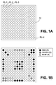
- an area array (BGA) pin field or map 10 for a BGA device with the pin locations PL-1, PL-2 PL-3 - PL-n are blank or not assigned.
- Fig. 1b shows the pin field map with mandatory fixed pin locations. For example pin locations designated by Rs (red) may be reserved for power input and those designated with Gs (green) may be reserved for ground connections. The pins designated by Bs (blue) may be reserved for highspeed buses, clocks, etc.
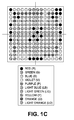
- Fig. 1c shows the area array pin field map with the remaining pins identified in the order of their routability with respect to pins previously reserved in Fig. 1b.
- the pin locations remaining in the periphery may be designated with a V (violet), The next most outer pin locations may be designated Os (orange) and LB (light brown). The remaining pins in the next most inner row of remaining pin locations may be designated with LBs and Ys (yellow). The next most inner row may be designated with Ys and LGs (light green). The next most row of remaining pin locations may be designated LGs and LBs (light blue). The remaining pins in the field may be designated by Ps (purple). Routability rankings not using color may be used.
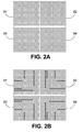
- Fig. 2a shows a blank area array for a BGA device with its pin field 11 divided into four sectors, 51, 52, 53, 54, each of which in this example are treated in the same fashion.
- suitable pin fields are identified in each sector as locations of potential routing channels. These pins may be designated as no connects or surface routing only pins to enable channel formation.
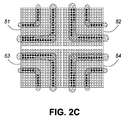
- Fig. 2c illustrates an area array (BGA) pin field with routing zones identified. These zones will channel a higher density of routing lines to increase the escape efficiency of the array.
- Fig. 2d shows an area array pin field with routing channels RC in place, serving to escape the array from the inside-out. It should be noted that all of these channels are needed to achieve the desired result.
- Fig. 3 shows such a PCB having BGA device (BGA-1, BGA-2, BGA-3, BGA-N, with pin lay outs as discussed above, mounted thereon and reduced layer count (surface layer (circuitry not shown), layer - 2,layer-3,layer-N).
- the invention has wide applicability to electronic systems in general. Even if a reduction of 2 (even 1) layers in out of every 10 PCB designs could have been achieved, a significant savings in PCB spending can be realized. This amount of reduction in layer count is well within the improvement provided by the invention according to example PCB studies.
Landscapes
- Engineering & Computer Science (AREA)
- Computer Hardware Design (AREA)
- Physics & Mathematics (AREA)
- Theoretical Computer Science (AREA)
- Microelectronics & Electronic Packaging (AREA)
- Evolutionary Computation (AREA)
- Geometry (AREA)
- General Engineering & Computer Science (AREA)
- General Physics & Mathematics (AREA)
- Design And Manufacture Of Integrated Circuits (AREA)
Abstract
Description
- The present application is related to the following U.S. patent applications which are assigned to the assignee hereof:
-
No. 10/991,360 filed November 19, 2004 -
No. 11/041,727 filed January 25, 2005 -
No. 11/200,041 filed August 10, 2005 -
No. 11/200,044 filed August 10, 2005 - High pin count devices, typically in excess of 1900 pins at 1mm pitch, are driving printed circuit boards (PCBs) to have upwards of 28 layers, which dramatically increases the cost of the card as well as increasing reliability problems, e.g. because such thick cards push through-hole board (THB) via technology to its limits resulting in manufacturing defects and failures caused by thermal expansion of the cards. In fact, for a typical circuit board, a 25% increase in the number of layers from 20 to 25 results in a 100% cost increase for example.
- Furthermore, although the cost of a circuit board is typically only about 14% of the printed board assembly (PBA) cost, the cost of a failed PCB is 100% of the PBA cost. This is because the entire PBA is usually scrapped when the PCB fails. Therefore, reducing the number of PCB failures saves more than just the cost of the PCB, which in the case of a 28 layer board is already a very significant cost savings.
- In addition, since PCB design is typically at the tail end of the PBA design process extra layers are often added to the PCB design to accommodate deficiencies in earlier stages of the PBA design. This practice further adds to the layer count, hence the cost, of a PCB. In fact, it is often a single component, usually a high pin count application specific integrated circuit (ASIC), that determines the maximum layer count of a PCB.
- In view of the foregoing, there is a need to provide a method of designing PCBs with lower layer counts, thereby reducing the manufacturing cost of PCBs while improving their reliability, which will also lead to cost savings with respect to PBA failures.
- High pin count custom devices such as ASICs usually determine the maximum layer count on a PCB. This in turn is usually determined by the pin-out of these devices because the pin-outs affect how easily the signals can be routed on the PCB. However, since little or no guidance to this effect is provided at the pin-out determination stage, each device pin-out is usually sub-optimal in terms of ease of routing the PCB. The only criteria that are usually considered are electrical or internal ASIC routing issues. Granted, these criteria are often more important than PCB routing, especially if they affect the operation of the ASIC. However, where multiple pin-out options exists that are equivalent under these criteria, there exists an opportunity to consider PCB routing issues, and possibly reduce the PCB layer count provided that some guidance is given to this end.
- It is an object of this invention to provide a system and method for optimizing the I/O pin usage of the PC board to thereby reduce the number of layers in a PC board. A further object of the invention is to provide an improved PCB design in which the pin-out of the PCB is improved without affecting the functionality thereof.
- The invention features a method for optimizing area array device pin utilization and reducing the number of layers on a multilayered PCB comprising:
- Preparing a package of BGA pin-out maps which anticipate the effect of existing fixed pins and derives the resulting optimum pin location assignment. The package of pin-out maps, in which each pin-out map includes an indication of the best routing for circuits from a given component to be mounted to a PCB.
- The said package of pin-out maps are also applied during the area array pin assignment phase, thereby making the area array package capable of supporting the optimum routing configuration proposed by the pin-out maps.
- Applying said package of pin-out maps during a PCB design phase so that the optimum circuit routing to each pin is achieved, thereby completing the strategy layed out by the proposed pin-out maps, resulting in a lower number of PCB layers.
- The invention further features the method discussed above wherein at least one of the pin-out maps shows areas of equal routing ease of escape for a selected device.
- The invention further features the method discussed above wherein at least one of said pin-out maps proposes areas within the area array to be left functionless so as to create channels (rows/columns) to aid in the efficient escape of a selected device type.
- The invention further features the method discussed above wherein at least one of said pin-out maps provides the designer/packaging house (ASIC/FPGA vendor) with the necessary pin-out information to make the area array pin grid compatible with said solution.
- The invention further features the method discussed above wherein at least one of said pin-out maps provides the PCB designer with the necessary routing information to leverage the pin-out configurations imparted above.
- The invention further features an automated tool/computer script which enables the methods detailed above.
- The invention further features an area array device (BGA) made in accordance with the methods defined above.
- Finally, the invention features a PCB made in accordance with the method defined above.
- The above and other objects, advantages and features of the invention will become more apparent when taken in conjunction with the following specification and accompanying drawings wherein:
- Fig. 1a is an illustration of a blank area array (BGA) pin field or map,
- Fig. 1b is an illustration of an area array (BGA) pin field or map with mandatory fixed pin locations identified,
- Fig. 1c is an illustration of an area array (BGA) pin field (map) with the remaining pins identified in the order of their routability respecting the fixed pins identified in Fig. 1b,
- Fig. 2a is an illustration of a blank area array pin field (map) wherein the pin field may be divided into four sectors,
- Fig. 2b is an illustration of an area array (BGA) pin field map with suitable pins identified in locations of potential routing channels,
- Fig. 2c is an illustration of an area array (BGA) pin field map with routing channel zones identified,
- Fig. 2d is an illustration of an area array (BGA) pin field map with routing channels in place and serving to escape the array from inside out, and
- Fig. 3 is an illustration of a printed circuit board with reduced layers made in accordance with the method of this invention.
- The invention provides package pin-out maps and a method of determining them. Each of the maps shows areas of equal routing ease for a given package type. Like areas are coded with the same color for manual pin-out determination, whereas they would have like numeral priority for an automated procedure. When determining the pin-out of a device, the areas of easiest routability are used first, and then areas of successively less routability as needed until all pin placements have been assigned. Some locations are predefined, such as power and ground pins, as well as high speed buses, clocks, etc. Areas of easiest routability are generally at the periphery of the package and ease of routability lessens towards inward layers barring any obstacles such as the aforementioned predefined locations. Maps can also be provided for no-connect (NC) pins to create channels for routing signal traces.
- As an example, a study was done on a typical PCB. With a worst case pin-out the PCB had 20 layers, which resulted in a $300 manufacturing cost. If the pin-out had been chosen randomly, the PCB would have needed 14 layers and cost $100 to produce. Applying the package pin-out maps, the layer count was reduced to only 8 layers, which resulted in a manufacturing cost of $20. This results in significant savings in layer count and cost relative to using a random pin-out.
- Referring to Fig. 1a, an area array (BGA) pin field or map 10 for a BGA device with the pin locations PL-1, PL-2 PL-3 - PL-n are blank or not assigned. Fig. 1b shows the pin field map with mandatory fixed pin locations. For example pin locations designated by Rs (red) may be reserved for power input and those designated with Gs (green) may be reserved for ground connections. The pins designated by Bs (blue) may be reserved for highspeed buses, clocks, etc. Fig. 1c shows the area array pin field map with the remaining pins identified in the order of their routability with respect to pins previously reserved in Fig. 1b. Keeping in mind that pin field areas of easiest routability are generally at the periphery, the pin locations remaining in the periphery may be designated with a V (violet), The next most outer pin locations may be designated Os (orange) and LB (light brown). The remaining pins in the next most inner row of remaining pin locations may be designated with LBs and Ys (yellow). The next most inner row may be designated with Ys and LGs (light green). The next most row of remaining pin locations may be designated LGs and LBs (light blue). The remaining pins in the field may be designated by Ps (purple). Routability rankings not using color may be used.
- Referring now to Figs. 2a-2d, Fig. 2a shows a blank area array for a BGA device with its pin field 11 divided into four sectors, 51, 52, 53, 54, each of which in this example are treated in the same fashion. In Fig. 2b, suitable pin fields are identified in each sector as locations of potential routing channels. These pins may be designated as no connects or surface routing only pins to enable channel formation. Fig. 2c illustrates an area array (BGA) pin field with routing zones identified. These zones will channel a higher density of routing lines to increase the escape efficiency of the array. Finally, Fig. 2d shows an area array pin field with routing channels RC in place, serving to escape the array from the inside-out. It should be noted that all of these channels are needed to achieve the desired result.
- After the package of BGA pin-out maps are prepared as described above, package of pin-out maps are applied during the area array pin out assignment phase, thereby area array package capable of supporting the optimum routing configuration proposed by the pin-out maps. The package of pin-out maps are then applied during the PCB design phase so that optimum circuit routing to each pin is achieved, thereby completing the strategy laid out by the pin-out maps, resulting in a lower number of PCB layers. Fig. 3 shows such a PCB having BGA device (BGA-1, BGA-2, BGA-3, BGA-N, with pin lay outs as discussed above, mounted thereon and reduced layer count (surface layer (circuitry not shown), layer - 2,layer-3,layer-N).
- - lowering PCB layer count saves manufacturing cost of the PCB, increases reliability of the PCB (e.g. less stress on THB vias)
- - lowering PCB cost also results in lower costs of PBA failures
- There has been disclosed and described a system for reducing the number of layers in a PC board and optimizing the pin usage of PC boards predicated on preparing a package of pin-out maps, each pin-out map showing areas of equal routing choices for selected devices of the type used in the PC board, using or applying the PC package of pin-out maps during PC board design phase so that the optimum circuit routing for each layer is achieved thereby resulting in a lower number of PCB layers.
- The invention has wide applicability to electronic systems in general. Even if a reduction of 2 (even 1) layers in out of every 10 PCB designs could have been achieved, a significant savings in PCB spending can be realized. This amount of reduction in layer count is well within the improvement provided by the invention according to example PCB studies.
- While the invention has been described in relation to preferred embodiments of the invention, it will be appreciated that other embodiments, adaptations and modifications of the invention will be apparent to those skilled in the art.
Claims (27)
- A method for optimizing area array device pin utilization and reducing the number of layers on a multilayered PCB comprising:preparing a package of BGA pin-out maps which anticipate the effect of existing fixed pins and derives the resulting optimum pin location assignment, said package of pin-out maps, in which each pin-out map includes an indication of the best routing for circuits from a given component to be mounted to a PCB, applying said package of pin-out maps during the area array pin assignment phase, thereby making the area array package capable of supporting the optimum routing configuration proposed by the pin-out maps, applying said package of pin-out maps during a PCB design phase so that the optimum circuit routing solution to each pin is achieved, thereby completing the strategy layed out by the proposed pin-out maps, resulting in a lower number of PCB layers.
- A method defined in claim 1 where at least one of said pin-out maps shows areas of equal routing ease of escape for a selected device.
- A method defined in claim 1 where at least one of said pin-out maps shows areas within the area array to be left functionless so as to create channels (rows/columns) to aid in the efficient escape of a selected device type.
- A method defined in claim 1 wherein at least one of said pin-out maps provides the designer and/or packaging house with the necessary pin-out information to make the area array pin grid compatible with a solution.
- The method defined in claim 1 wherein at least one of said pin-out maps provides the PCB designer with the necessary routing information to leverage the pin-out configurations.
- An automated tool/computer script which enables the methods defined in claim 1.
- An area array device (BGA) made in accordance with the methods defined in claim 1.
- A PCB made in accordance with the method defined in claim 1.
- Method for optimizing area array device pin utilization and reducing the number of layers on a multilayered PCB comprising:preparing a package of BGA pin-out maps which anticipate the effect of existing fixed pins and derives the resulting optimum pin location assignment, said package of pin-out maps, in which each pin-out map includes an indication of the best routing for circuits from a given component to be mounted to a PCB, andapplying said package of pin-out maps during the area array pin assignment phase, thereby making the area array package capable of supporting the optimum routing configuration proposed by the pin-out maps.
- Method defined in claim 9 where at least one of the pin-out maps shows areas of equal routing ease of escape for a selected device.
- Method defined in claim 9 where at least one of said pin-out maps proposes areas within the area array to be left functionless so as to create channels (rows/columns) to aid in the efficient escape of a selected device type.
- A method defined in claim 9 wherein at least one of said pin-out maps provides the designer/ packaging house (ASIC/FPGA vendor) with the necessary pin-out information to make the area array pin grid compatible therewith.
- The method defined in claim 9 wherein at least one of said pin-out maps provides the PCB designer with the necessary routing information to leverage the pin-out configurations.
- An area array device (BGA) made in accordance with the method defined in claim 9.
- Method for optimizing area array device pin utilization and reducing the number of layers on a multilayered PCB comprising:preparing a package of BGA pin-out maps which anticipate the effect of existing fixed pins and derives the resulting optimum pin location assignment, said package of pin-out maps, in which each pin-out map includes an indication of the best routing for circuits from a given component to be mounted to a PCB, andapplying said package of pin-out maps during a PCB design phase so that the optimum circuit routing to each pin is achieved, thereby completing the strategy layed out by the proposed pin-out maps, resulting in a lower number of PCB layers.
- Method defined in claim 15 where at least one of the pin-out maps shows areas of equal routing ease of escape for a selected device.
- Method defined in claim 15 where at least one of said pin-out maps proposes areas within the area array to be left functionless so as to create channels (rows/columns)to aid in the efficient escape of a selected device type.
- A method defined in claim 15 wherein at least one of said pin-out maps provides the designer/packaging house (ASIC/FPGA vendor) with the necessary pin-out information to make the area array pin grid compatible therewith.
- The method defined in claim 1 wherein at least one of said pin-out maps provides the PCB designer with the necessary routing information to leverage the pin-out configurations.
- A PCB made in accordance with the method defined in claim 15.
- A method for reducing the number of layers and optimizing the pin utilization on a layered PCB (printed circuit board) comprising:preparing a package of pin-out maps, each said pin-out map including an indication of the best routing for circuits from a given component to be mounted on the PCB;applying said package of pin-out maps during a PCB design phase so that the optimum circuit routing to each pin-out is achieved thereby resulting in a lower number of PCB layers.
- The method defined in claim 21 wherein at least one of said pin-out maps shows areas of equal routing ease of escape for a selected device type.
- The method defined in claim 21 wherein at least one of said pin-out maps provides the PCB designer with routing information.
- A PCB made according to the method defined in claim 21.
- A package of BGA pin-out maps which anticipate the effect of existing fixed pins and derives the resulting optimum pin location assignment,in which each pin-out map includes an indication of the best routing for circuits from a given component to be mounted to a PCB.
- The package defined in claim 1 where at least one of the pin-out maps shows areas of equal routing ease of escape for a selected device.
- The package defined in claim 1 where at least one of said pin-out maps proposes areas within the area array to be left functionless so as to create channels (rows/columns) to aid in the efficient escape of a selected device type.
Applications Claiming Priority (1)
| Application Number | Priority Date | Filing Date | Title |
|---|---|---|---|
| US11/224,012 US7343577B2 (en) | 2005-09-13 | 2005-09-13 | Area array routing masks for improved escape of devices on PCB |
Publications (1)
| Publication Number | Publication Date |
|---|---|
| EP1763294A1 true EP1763294A1 (en) | 2007-03-14 |
Family
ID=37488006
Family Applications (1)
| Application Number | Title | Priority Date | Filing Date |
|---|---|---|---|
| EP06300939A Withdrawn EP1763294A1 (en) | 2005-09-13 | 2006-09-12 | Area array routing masks for improved escape of devices on PCB |
Country Status (3)
| Country | Link |
|---|---|
| US (1) | US7343577B2 (en) |
| EP (1) | EP1763294A1 (en) |
| CN (1) | CN1940946A (en) |
Families Citing this family (13)
| Publication number | Priority date | Publication date | Assignee | Title |
|---|---|---|---|---|
| WO2008058258A2 (en) * | 2006-11-08 | 2008-05-15 | Mentor Graphics Corporation | Use of breakouts in printed circuit board designs |
| US7797663B2 (en) * | 2007-04-04 | 2010-09-14 | Cisco Technology, Inc. | Conductive dome probes for measuring system level multi-GHZ signals |
| US7624211B2 (en) * | 2007-06-27 | 2009-11-24 | Micron Technology, Inc. | Method for bus width negotiation of data storage devices |
| WO2014056201A1 (en) * | 2012-10-12 | 2014-04-17 | Mediatek Inc. | Layout module for printed circuit board |
| US9345137B2 (en) * | 2013-11-04 | 2016-05-17 | Lattice Semiconductor Corporation | Partially depopulated interconnection arrays for packaged semiconductor devices and printed circuit boards |
| CN105574237B (en) * | 2015-12-10 | 2018-12-21 | 广东顺德中山大学卡内基梅隆大学国际联合研究院 | System in package BGA power ground pin distribution optimization method based on population |
| CN105608257B (en) * | 2015-12-15 | 2018-12-21 | 广东顺德中山大学卡内基梅隆大学国际联合研究院 | The optimal pin of extensive BGA package based on genetic algorithm is distributed generation method |
| CN109600911B (en) * | 2018-12-05 | 2021-04-20 | 郑州云海信息技术有限公司 | A method for arranging signal pins of a PCB connector and a related device |
| CN109858185B (en) * | 2019-03-08 | 2022-09-02 | 广东岭南职业技术学院 | Indoor decoration design method based on AR virtual reality technology |
| CN111141954B (en) * | 2020-01-02 | 2022-05-06 | 北京半导体专用设备研究所(中国电子科技集团公司第四十五研究所) | Test file generation method and device of resistor network and electronic equipment |
| US11817378B2 (en) * | 2020-07-08 | 2023-11-14 | Qualcomm Incorporated | Apparatus and method for providing a scalable ball grid array (BGA) assignment and a PCB circuit trace breakout pattern for RF chip interfaces |
| CN114647999B (en) * | 2022-03-16 | 2024-11-08 | 武汉理工大学 | A staggered pin matrix escape wiring method |
| CN120124580B (en) * | 2025-02-21 | 2025-12-05 | 福州大学 | A Differential Pair Ordered Escape Wiring Method Based on Improved Monte Carlo Tree Search |
Citations (4)
| Publication number | Priority date | Publication date | Assignee | Title |
|---|---|---|---|---|
| EP1075026A2 (en) * | 1999-08-06 | 2001-02-07 | Shinko Electric Industries Co. Ltd. | Multilayer circuit board layout |
| US6521846B1 (en) * | 2002-01-07 | 2003-02-18 | Sun Microsystems, Inc. | Method for assigning power and ground pins in array packages to enhance next level routing |
| EP1434473A2 (en) * | 2002-12-23 | 2004-06-30 | Nortel Networks Limited | Technique for reducing the number of layers in a signal routing device |
| US20040212103A1 (en) * | 2000-06-19 | 2004-10-28 | Herman Kwong | Techniques for pin arrangements in circuit chips |
Family Cites Families (4)
| Publication number | Priority date | Publication date | Assignee | Title |
|---|---|---|---|---|
| JP3571369B2 (en) * | 1994-06-16 | 2004-09-29 | 富士通株式会社 | Wiring design equipment |
| JPH11110434A (en) * | 1997-10-07 | 1999-04-23 | Fujitsu Ltd | Printed circuit board pattern design equipment |
| US7114132B2 (en) * | 2001-04-20 | 2006-09-26 | Nec Corporation | Device, system, server, client, and method for supporting component layout design on circuit board, and program for implementing the device |
| US7594215B2 (en) * | 2004-11-20 | 2009-09-22 | Cadence Design Systems, Inc. | Method and system for optimized automated IC package pin routing |
-
2005
- 2005-09-13 US US11/224,012 patent/US7343577B2/en not_active Expired - Fee Related
-
2006
- 2006-09-12 EP EP06300939A patent/EP1763294A1/en not_active Withdrawn
- 2006-09-13 CN CNA2006101431556A patent/CN1940946A/en active Pending
Patent Citations (4)
| Publication number | Priority date | Publication date | Assignee | Title |
|---|---|---|---|---|
| EP1075026A2 (en) * | 1999-08-06 | 2001-02-07 | Shinko Electric Industries Co. Ltd. | Multilayer circuit board layout |
| US20040212103A1 (en) * | 2000-06-19 | 2004-10-28 | Herman Kwong | Techniques for pin arrangements in circuit chips |
| US6521846B1 (en) * | 2002-01-07 | 2003-02-18 | Sun Microsystems, Inc. | Method for assigning power and ground pins in array packages to enhance next level routing |
| EP1434473A2 (en) * | 2002-12-23 | 2004-06-30 | Nortel Networks Limited | Technique for reducing the number of layers in a signal routing device |
Also Published As
| Publication number | Publication date |
|---|---|
| US7343577B2 (en) | 2008-03-11 |
| US20070057362A1 (en) | 2007-03-15 |
| CN1940946A (en) | 2007-04-04 |
Similar Documents
| Publication | Publication Date | Title |
|---|---|---|
| US7343577B2 (en) | Area array routing masks for improved escape of devices on PCB | |
| US7757196B2 (en) | Optimizing application specific integrated circuit pinouts for high density interconnect printed circuit boards | |
| US7979983B2 (en) | Connection an integrated circuit on a surface layer of a printed circuit board | |
| US7831949B2 (en) | Method of designing semiconductor integrated circuit, designing apparatus, semiconductor integrated circuit system, semiconductor integrated circuit mounting substrate, package and semiconductor integrated circuit | |
| EP1812967B1 (en) | Off-width pitch for improved circuit card routing | |
| US6047469A (en) | Method of connecting a unit under test in a wireless test fixture | |
| KR20020001582A (en) | Semiconductor Integrated Circuit and Semiconductor Integrated Circuit Wiring Layout Method | |
| US7714234B2 (en) | Alternating micro-vias and throughboard vias to create PCB routing channels in BGA interconnect grid | |
| US5856636A (en) | Electronic circuit prototype wiring board with visually distinctive contact pads | |
| US6671865B1 (en) | High density input output | |
| CN1913747B (en) | Using rows/columns of micro-vias in a BGA interconnect grid to create improved PCB routing channels | |
| US9345132B2 (en) | Substrate structure and the process manufacturing the same | |
| US20030102159A1 (en) | Optimum power and ground bump pad and bump patterns for flip chip packaging | |
| US7024637B2 (en) | Functionality based package design for integrated circuit blocks | |
| CN101808479B (en) | Technique for reducing the number of layers in multilayer circuit board | |
| US20070248800A1 (en) | Multilayer board having layer configuration indicator portion | |
| CN210641126U (en) | PCB board | |
| WO2007050989A2 (en) | System and method for modular electronics design | |
| US20100077608A1 (en) | Alternating Via Fanout Patterns | |
| Li | Cavity, Chip Stack and TSV Design | |
| CN106709154A (en) | Method for reducing modification layers during integrated circuit engineering modification | |
| JPH1019992A (en) | Memory circuit having wiring path suitable for mounting test, test method therefor, and wiring apparatus | |
| Holden | The New IPC HDI (Microvia) Design Guideline (IPC-2315) | |
| JPH06177249A (en) | Integrated circuit device | |
| JPH02245830A (en) | Automatic wiring method for printed board |
Legal Events
| Date | Code | Title | Description |
|---|---|---|---|
| PUAI | Public reference made under article 153(3) epc to a published international application that has entered the european phase |
Free format text: ORIGINAL CODE: 0009012 |
|
| AK | Designated contracting states |
Kind code of ref document: A1 Designated state(s): AT BE BG CH CY CZ DE DK EE ES FI FR GB GR HU IE IS IT LI LT LU LV MC NL PL PT RO SE SI SK TR |
|
| AX | Request for extension of the european patent |
Extension state: AL BA HR MK YU |
|
| RAP1 | Party data changed (applicant data changed or rights of an application transferred) |
Owner name: ALCATEL LUCENT |
|
| 17P | Request for examination filed |
Effective date: 20070914 |
|
| 17Q | First examination report despatched |
Effective date: 20071018 |
|
| AKX | Designation fees paid |
Designated state(s): AT BE BG CH CY CZ DE DK EE ES FI FR GB GR HU IE IS IT LI LT LU LV MC NL PL PT RO SE SI SK TR |
|
| STAA | Information on the status of an ep patent application or granted ep patent |
Free format text: STATUS: THE APPLICATION IS DEEMED TO BE WITHDRAWN |
|
| 18D | Application deemed to be withdrawn |
Effective date: 20110401 |