EP1763075A1 - Methode für die präzise Vereinzelung von integrierten Schaltungen unter Verwendung von differentiellen Ätzraten - Google Patents
Methode für die präzise Vereinzelung von integrierten Schaltungen unter Verwendung von differentiellen Ätzraten Download PDFInfo
- Publication number
- EP1763075A1 EP1763075A1 EP05108400A EP05108400A EP1763075A1 EP 1763075 A1 EP1763075 A1 EP 1763075A1 EP 05108400 A EP05108400 A EP 05108400A EP 05108400 A EP05108400 A EP 05108400A EP 1763075 A1 EP1763075 A1 EP 1763075A1
- Authority
- EP
- European Patent Office
- Prior art keywords
- etching process
- singulation
- depth
- integrated circuit
- wafer
- Prior art date
- Legal status (The legal status is an assumption and is not a legal conclusion. Google has not performed a legal analysis and makes no representation as to the accuracy of the status listed.)
- Withdrawn
Links
- 238000000034 method Methods 0.000 title claims abstract description 77
- 230000008569 process Effects 0.000 claims abstract description 46
- 239000004065 semiconductor Substances 0.000 claims abstract description 34
- 239000000758 substrate Substances 0.000 claims abstract description 31
- 238000005530 etching Methods 0.000 claims description 41
- 238000000708 deep reactive-ion etching Methods 0.000 claims description 16
- 238000001020 plasma etching Methods 0.000 claims description 11
- 229910052782 aluminium Inorganic materials 0.000 claims description 4
- XAGFODPZIPBFFR-UHFFFAOYSA-N aluminium Chemical compound [Al] XAGFODPZIPBFFR-UHFFFAOYSA-N 0.000 claims description 4
- 229910052751 metal Inorganic materials 0.000 abstract description 11
- 239000002184 metal Substances 0.000 abstract description 11
- 239000000463 material Substances 0.000 abstract description 7
- 239000010410 layer Substances 0.000 description 27
- 238000002161 passivation Methods 0.000 description 9
- VYPSYNLAJGMNEJ-UHFFFAOYSA-N silicon dioxide Inorganic materials O=[Si]=O VYPSYNLAJGMNEJ-UHFFFAOYSA-N 0.000 description 9
- XUIMIQQOPSSXEZ-UHFFFAOYSA-N Silicon Chemical compound [Si] XUIMIQQOPSSXEZ-UHFFFAOYSA-N 0.000 description 8
- 238000012545 processing Methods 0.000 description 8
- 229910052710 silicon Inorganic materials 0.000 description 8
- 239000010703 silicon Substances 0.000 description 8
- 238000004519 manufacturing process Methods 0.000 description 6
- 229910052814 silicon oxide Inorganic materials 0.000 description 6
- 229920002120 photoresistant polymer Polymers 0.000 description 4
- 238000003491 array Methods 0.000 description 3
- 150000002500 ions Chemical class 0.000 description 3
- 238000000059 patterning Methods 0.000 description 3
- 230000000149 penetrating effect Effects 0.000 description 3
- 239000000126 substance Substances 0.000 description 3
- 230000008901 benefit Effects 0.000 description 2
- 235000008429 bread Nutrition 0.000 description 2
- 238000006243 chemical reaction Methods 0.000 description 2
- 238000010276 construction Methods 0.000 description 2
- 238000005520 cutting process Methods 0.000 description 2
- 230000001419 dependent effect Effects 0.000 description 2
- 238000005498 polishing Methods 0.000 description 2
- 235000012239 silicon dioxide Nutrition 0.000 description 2
- 238000006467 substitution reaction Methods 0.000 description 2
- 238000012360 testing method Methods 0.000 description 2
- VYZAMTAEIAYCRO-UHFFFAOYSA-N Chromium Chemical compound [Cr] VYZAMTAEIAYCRO-UHFFFAOYSA-N 0.000 description 1
- 230000004075 alteration Effects 0.000 description 1
- 230000004888 barrier function Effects 0.000 description 1
- 239000003990 capacitor Substances 0.000 description 1
- 238000003486 chemical etching Methods 0.000 description 1
- 239000002131 composite material Substances 0.000 description 1
- 238000000151 deposition Methods 0.000 description 1
- 230000008021 deposition Effects 0.000 description 1
- 238000013461 design Methods 0.000 description 1
- 239000002019 doping agent Substances 0.000 description 1
- 230000000694 effects Effects 0.000 description 1
- 238000005538 encapsulation Methods 0.000 description 1
- 229910052731 fluorine Inorganic materials 0.000 description 1
- 239000011737 fluorine Substances 0.000 description 1
- NBVXSUQYWXRMNV-UHFFFAOYSA-N fluoromethane Chemical compound FC NBVXSUQYWXRMNV-UHFFFAOYSA-N 0.000 description 1
- 239000007789 gas Substances 0.000 description 1
- 239000011521 glass Substances 0.000 description 1
- 238000000227 grinding Methods 0.000 description 1
- 238000009413 insulation Methods 0.000 description 1
- 238000010297 mechanical methods and process Methods 0.000 description 1
- 239000007769 metal material Substances 0.000 description 1
- 238000001465 metallisation Methods 0.000 description 1
- 238000012986 modification Methods 0.000 description 1
- 230000004048 modification Effects 0.000 description 1
- 230000003287 optical effect Effects 0.000 description 1
- 239000001301 oxygen Substances 0.000 description 1
- 229910052760 oxygen Inorganic materials 0.000 description 1
- 238000007747 plating Methods 0.000 description 1
- 229910021420 polycrystalline silicon Inorganic materials 0.000 description 1
- 229920005591 polysilicon Polymers 0.000 description 1
- 239000011241 protective layer Substances 0.000 description 1
- 239000010453 quartz Substances 0.000 description 1
- 238000000926 separation method Methods 0.000 description 1
- 239000000377 silicon dioxide Substances 0.000 description 1
- 230000002269 spontaneous effect Effects 0.000 description 1
Images


Classifications
-
- H—ELECTRICITY
- H01—ELECTRIC ELEMENTS
- H01L—SEMICONDUCTOR DEVICES NOT COVERED BY CLASS H10
- H01L27/00—Devices consisting of a plurality of semiconductor or other solid-state components formed in or on a common substrate
- H01L27/14—Devices consisting of a plurality of semiconductor or other solid-state components formed in or on a common substrate including semiconductor components sensitive to infrared radiation, light, electromagnetic radiation of shorter wavelength or corpuscular radiation and specially adapted either for the conversion of the energy of such radiation into electrical energy or for the control of electrical energy by such radiation
- H01L27/144—Devices controlled by radiation
- H01L27/146—Imager structures
- H01L27/14683—Processes or apparatus peculiar to the manufacture or treatment of these devices or parts thereof
-
- H—ELECTRICITY
- H01—ELECTRIC ELEMENTS
- H01L—SEMICONDUCTOR DEVICES NOT COVERED BY CLASS H10
- H01L21/00—Processes or apparatus adapted for the manufacture or treatment of semiconductor or solid state devices or of parts thereof
- H01L21/70—Manufacture or treatment of devices consisting of a plurality of solid state components formed in or on a common substrate or of parts thereof; Manufacture of integrated circuit devices or of parts thereof
- H01L21/77—Manufacture or treatment of devices consisting of a plurality of solid state components or integrated circuits formed in, or on, a common substrate
- H01L21/78—Manufacture or treatment of devices consisting of a plurality of solid state components or integrated circuits formed in, or on, a common substrate with subsequent division of the substrate into plural individual devices
Definitions
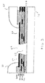
- a predetermined portion 70 of second surface 10 is removed slightly beyond the depth of singulation channel 65, such as by lapping, grinding, polishing or chemical mechanical polishing (CMP) or equivalent processes as are well known in the semiconductor arts.
- CMP chemical mechanical polishing
Landscapes
- Engineering & Computer Science (AREA)
- Physics & Mathematics (AREA)
- Power Engineering (AREA)
- Condensed Matter Physics & Semiconductors (AREA)
- General Physics & Mathematics (AREA)
- Computer Hardware Design (AREA)
- Microelectronics & Electronic Packaging (AREA)
- Electromagnetism (AREA)
- Manufacturing & Machinery (AREA)
- Dicing (AREA)
Priority Applications (1)
| Application Number | Priority Date | Filing Date | Title |
|---|---|---|---|
| EP05108400A EP1763075A1 (de) | 2005-09-13 | 2005-09-13 | Methode für die präzise Vereinzelung von integrierten Schaltungen unter Verwendung von differentiellen Ätzraten |
Applications Claiming Priority (1)
| Application Number | Priority Date | Filing Date | Title |
|---|---|---|---|
| EP05108400A EP1763075A1 (de) | 2005-09-13 | 2005-09-13 | Methode für die präzise Vereinzelung von integrierten Schaltungen unter Verwendung von differentiellen Ätzraten |
Publications (1)
| Publication Number | Publication Date |
|---|---|
| EP1763075A1 true EP1763075A1 (de) | 2007-03-14 |
Family
ID=35709008
Family Applications (1)
| Application Number | Title | Priority Date | Filing Date |
|---|---|---|---|
| EP05108400A Withdrawn EP1763075A1 (de) | 2005-09-13 | 2005-09-13 | Methode für die präzise Vereinzelung von integrierten Schaltungen unter Verwendung von differentiellen Ätzraten |
Country Status (1)
| Country | Link |
|---|---|
| EP (1) | EP1763075A1 (de) |
Cited By (4)
| Publication number | Priority date | Publication date | Assignee | Title |
|---|---|---|---|---|
| EP2315248A1 (de) * | 2009-10-26 | 2011-04-27 | Fondazione Bruno Kessler | Verfahren zur Herstellung eines Halbleitersensors und erhaltener Sensor |
| EP2693480A1 (de) * | 2011-03-31 | 2014-02-05 | Hamamatsu Photonics K.K. | Lichtdiodenarray-modul und herstellungsverfahren dafür |
| DE102011055224B4 (de) | 2010-11-15 | 2018-09-27 | Infineon Technologies Ag | Verfahren zum Herstellen eines Halbleiterchips und ein Halbleiterchip |
| CN111079281A (zh) * | 2019-12-11 | 2020-04-28 | 北京华大九天软件有限公司 | 一种分割版图并生成随机图形的方法 |
Citations (6)
| Publication number | Priority date | Publication date | Assignee | Title |
|---|---|---|---|---|
| US5259925A (en) | 1992-06-05 | 1993-11-09 | Mcdonnell Douglas Corporation | Method of cleaning a plurality of semiconductor devices |
| DE4241045C1 (de) * | 1992-12-05 | 1994-05-26 | Bosch Gmbh Robert | Verfahren zum anisotropen Ätzen von Silicium |
| US6174789B1 (en) * | 1998-02-20 | 2001-01-16 | Nec Corporation | Method of dividing a compound semiconductor wafer into pellets by utilizing extremely narrow scribe regions |
| US6177352B1 (en) | 1996-08-13 | 2001-01-23 | Siemens Aktiengesellschaft | Method for producing semiconductor bodies with an MOVPE layer sequence |
| EP1394851A2 (de) | 2002-09-02 | 2004-03-03 | Shinko Electric Industries Co. Ltd. | Halbleiterchip und Herstellungsverfahren dafür |
| US6756288B1 (en) * | 1999-07-01 | 2004-06-29 | Fraunhofer-Gesellschaft Zur Foerderung Der Angewandten Forschung E.V. | Method of subdividing a wafer |
-
2005
- 2005-09-13 EP EP05108400A patent/EP1763075A1/de not_active Withdrawn
Patent Citations (6)
| Publication number | Priority date | Publication date | Assignee | Title |
|---|---|---|---|---|
| US5259925A (en) | 1992-06-05 | 1993-11-09 | Mcdonnell Douglas Corporation | Method of cleaning a plurality of semiconductor devices |
| DE4241045C1 (de) * | 1992-12-05 | 1994-05-26 | Bosch Gmbh Robert | Verfahren zum anisotropen Ätzen von Silicium |
| US6177352B1 (en) | 1996-08-13 | 2001-01-23 | Siemens Aktiengesellschaft | Method for producing semiconductor bodies with an MOVPE layer sequence |
| US6174789B1 (en) * | 1998-02-20 | 2001-01-16 | Nec Corporation | Method of dividing a compound semiconductor wafer into pellets by utilizing extremely narrow scribe regions |
| US6756288B1 (en) * | 1999-07-01 | 2004-06-29 | Fraunhofer-Gesellschaft Zur Foerderung Der Angewandten Forschung E.V. | Method of subdividing a wafer |
| EP1394851A2 (de) | 2002-09-02 | 2004-03-03 | Shinko Electric Industries Co. Ltd. | Halbleiterchip und Herstellungsverfahren dafür |
Cited By (6)
| Publication number | Priority date | Publication date | Assignee | Title |
|---|---|---|---|---|
| EP2315248A1 (de) * | 2009-10-26 | 2011-04-27 | Fondazione Bruno Kessler | Verfahren zur Herstellung eines Halbleitersensors und erhaltener Sensor |
| DE102011055224B4 (de) | 2010-11-15 | 2018-09-27 | Infineon Technologies Ag | Verfahren zum Herstellen eines Halbleiterchips und ein Halbleiterchip |
| EP2693480A1 (de) * | 2011-03-31 | 2014-02-05 | Hamamatsu Photonics K.K. | Lichtdiodenarray-modul und herstellungsverfahren dafür |
| EP2693480A4 (de) * | 2011-03-31 | 2014-10-01 | Hamamatsu Photonics Kk | Lichtdiodenarray-modul und herstellungsverfahren dafür |
| US9496298B2 (en) | 2011-03-31 | 2016-11-15 | Hamamatsu Photonics K.K. | Photodiode array module and method for manufacturing same |
| CN111079281A (zh) * | 2019-12-11 | 2020-04-28 | 北京华大九天软件有限公司 | 一种分割版图并生成随机图形的方法 |
Similar Documents
| Publication | Publication Date | Title |
|---|---|---|
| US7335576B2 (en) | Method for precision integrated circuit die singulation using differential etch rates | |
| US6521513B1 (en) | Silicon wafer configuration and method for forming same | |
| US9196511B2 (en) | Semiconductor die singulation methods | |
| US8962452B2 (en) | Semiconductor die singulation apparatus and method | |
| US9589812B2 (en) | Fabrication method of semiconductor piece | |
| JP5637329B1 (ja) | 半導体片の製造方法、半導体片を含む回路基板および画像形成装置 | |
| JP5817905B1 (ja) | 半導体片の製造方法 | |
| US20090061595A1 (en) | Method for dividing a semiconductor substrate and a method for producing a semiconductor circuit arrangement | |
| KR100855015B1 (ko) | 패키징된 집적회로 및 그 제조 방법 | |
| US8030180B2 (en) | Method of manufacturing a semiconductor device | |
| US8637967B2 (en) | Method for fabricating a semiconductor chip and semiconductor chip | |
| US11767219B2 (en) | Semiconductor structure including scribe line structures and method for fabricating the same | |
| KR101116993B1 (ko) | 집적 회로의 제조 방법 | |
| US20150243561A1 (en) | Semiconductor Devices and Methods of Formation Thereof | |
| EP1763075A1 (de) | Methode für die präzise Vereinzelung von integrierten Schaltungen unter Verwendung von differentiellen Ätzraten | |
| US20170084468A1 (en) | Method for processing a wafer and method for dicing a wafer | |
| KR101192526B1 (ko) | 웨이퍼로부터 반도체 칩을 제조하기 위한 방법 및 반도체 구성 요소 | |
| KR20070074937A (ko) | 스크라이브 레인의 트렌치를 이용한 반도체 웨이퍼의다이싱 방법 | |
| JP2007049066A (ja) | 半導体ウェハ、並びに、半導体チップおよびその製造方法 | |
| US20050124140A1 (en) | Pre-fabrication scribing | |
| WO2005119747A2 (en) | Semiconductor wafer with ditched scribe street | |
| JPS61267343A (ja) | 半導体装置の製造方法 | |
| CN111977610A (zh) | 微机电系统及其制造方法 | |
| US20230274979A1 (en) | Plasma diced wafers and methods thereof | |
| GB2102202A (en) | Semiconductor device passivation |
Legal Events
| Date | Code | Title | Description |
|---|---|---|---|
| PUAI | Public reference made under article 153(3) epc to a published international application that has entered the european phase |
Free format text: ORIGINAL CODE: 0009012 |
|
| AK | Designated contracting states |
Kind code of ref document: A1 Designated state(s): AT BE BG CH CY CZ DE DK EE ES FI FR GB GR HU IE IS IT LI LT LU LV MC NL PL PT RO SE SI SK TR |
|
| AX | Request for extension of the european patent |
Extension state: AL BA HR MK YU |
|
| 17P | Request for examination filed |
Effective date: 20070824 |
|
| 17Q | First examination report despatched |
Effective date: 20071004 |
|
| AKX | Designation fees paid |
Designated state(s): AT BE BG CH CY CZ DE DK EE ES FI FR GB GR HU IE IS IT LI LT LU LV MC NL PL PT RO SE SI SK TR |
|
| STAA | Information on the status of an ep patent application or granted ep patent |
Free format text: STATUS: THE APPLICATION IS DEEMED TO BE WITHDRAWN |
|
| 18D | Application deemed to be withdrawn |
Effective date: 20100402 |