EP1762884B1 - Liquid crystal display - Google Patents
Liquid crystal display Download PDFInfo
- Publication number
- EP1762884B1 EP1762884B1 EP06018191A EP06018191A EP1762884B1 EP 1762884 B1 EP1762884 B1 EP 1762884B1 EP 06018191 A EP06018191 A EP 06018191A EP 06018191 A EP06018191 A EP 06018191A EP 1762884 B1 EP1762884 B1 EP 1762884B1
- Authority
- EP
- European Patent Office
- Prior art keywords
- electrode
- liquid crystal
- subpixel
- crystal display
- electrodes
- Prior art date
- Legal status (The legal status is an assumption and is not a legal conclusion. Google has not performed a legal analysis and makes no representation as to the accuracy of the status listed.)
- Not-in-force
Links
Images


Classifications
-
- G—PHYSICS
- G02—OPTICS
- G02F—OPTICAL DEVICES OR ARRANGEMENTS FOR THE CONTROL OF LIGHT BY MODIFICATION OF THE OPTICAL PROPERTIES OF THE MEDIA OF THE ELEMENTS INVOLVED THEREIN; NON-LINEAR OPTICS; FREQUENCY-CHANGING OF LIGHT; OPTICAL LOGIC ELEMENTS; OPTICAL ANALOGUE/DIGITAL CONVERTERS
- G02F1/00—Devices or arrangements for the control of the intensity, colour, phase, polarisation or direction of light arriving from an independent light source, e.g. switching, gating or modulating; Non-linear optics
- G02F1/01—Devices or arrangements for the control of the intensity, colour, phase, polarisation or direction of light arriving from an independent light source, e.g. switching, gating or modulating; Non-linear optics for the control of the intensity, phase, polarisation or colour
- G02F1/13—Devices or arrangements for the control of the intensity, colour, phase, polarisation or direction of light arriving from an independent light source, e.g. switching, gating or modulating; Non-linear optics for the control of the intensity, phase, polarisation or colour based on liquid crystals, e.g. single liquid crystal display cells
- G02F1/137—Devices or arrangements for the control of the intensity, colour, phase, polarisation or direction of light arriving from an independent light source, e.g. switching, gating or modulating; Non-linear optics for the control of the intensity, phase, polarisation or colour based on liquid crystals, e.g. single liquid crystal display cells characterised by the electro-optical or magneto-optical effect, e.g. field-induced phase transition, orientation effect, guest-host interaction or dynamic scattering
- G02F1/139—Devices or arrangements for the control of the intensity, colour, phase, polarisation or direction of light arriving from an independent light source, e.g. switching, gating or modulating; Non-linear optics for the control of the intensity, phase, polarisation or colour based on liquid crystals, e.g. single liquid crystal display cells characterised by the electro-optical or magneto-optical effect, e.g. field-induced phase transition, orientation effect, guest-host interaction or dynamic scattering based on orientation effects in which the liquid crystal remains transparent
- G02F1/1393—Devices or arrangements for the control of the intensity, colour, phase, polarisation or direction of light arriving from an independent light source, e.g. switching, gating or modulating; Non-linear optics for the control of the intensity, phase, polarisation or colour based on liquid crystals, e.g. single liquid crystal display cells characterised by the electro-optical or magneto-optical effect, e.g. field-induced phase transition, orientation effect, guest-host interaction or dynamic scattering based on orientation effects in which the liquid crystal remains transparent the birefringence of the liquid crystal being electrically controlled, e.g. ECB-, DAP-, HAN-, PI-LC cells
-
- G—PHYSICS
- G02—OPTICS
- G02F—OPTICAL DEVICES OR ARRANGEMENTS FOR THE CONTROL OF LIGHT BY MODIFICATION OF THE OPTICAL PROPERTIES OF THE MEDIA OF THE ELEMENTS INVOLVED THEREIN; NON-LINEAR OPTICS; FREQUENCY-CHANGING OF LIGHT; OPTICAL LOGIC ELEMENTS; OPTICAL ANALOGUE/DIGITAL CONVERTERS
- G02F1/00—Devices or arrangements for the control of the intensity, colour, phase, polarisation or direction of light arriving from an independent light source, e.g. switching, gating or modulating; Non-linear optics
- G02F1/01—Devices or arrangements for the control of the intensity, colour, phase, polarisation or direction of light arriving from an independent light source, e.g. switching, gating or modulating; Non-linear optics for the control of the intensity, phase, polarisation or colour
- G02F1/13—Devices or arrangements for the control of the intensity, colour, phase, polarisation or direction of light arriving from an independent light source, e.g. switching, gating or modulating; Non-linear optics for the control of the intensity, phase, polarisation or colour based on liquid crystals, e.g. single liquid crystal display cells
- G02F1/133—Constructional arrangements; Operation of liquid crystal cells; Circuit arrangements
- G02F1/1333—Constructional arrangements; Manufacturing methods
- G02F1/1343—Electrodes
-
- G—PHYSICS
- G02—OPTICS
- G02F—OPTICAL DEVICES OR ARRANGEMENTS FOR THE CONTROL OF LIGHT BY MODIFICATION OF THE OPTICAL PROPERTIES OF THE MEDIA OF THE ELEMENTS INVOLVED THEREIN; NON-LINEAR OPTICS; FREQUENCY-CHANGING OF LIGHT; OPTICAL LOGIC ELEMENTS; OPTICAL ANALOGUE/DIGITAL CONVERTERS
- G02F1/00—Devices or arrangements for the control of the intensity, colour, phase, polarisation or direction of light arriving from an independent light source, e.g. switching, gating or modulating; Non-linear optics
- G02F1/01—Devices or arrangements for the control of the intensity, colour, phase, polarisation or direction of light arriving from an independent light source, e.g. switching, gating or modulating; Non-linear optics for the control of the intensity, phase, polarisation or colour
- G02F1/13—Devices or arrangements for the control of the intensity, colour, phase, polarisation or direction of light arriving from an independent light source, e.g. switching, gating or modulating; Non-linear optics for the control of the intensity, phase, polarisation or colour based on liquid crystals, e.g. single liquid crystal display cells
- G02F1/133—Constructional arrangements; Operation of liquid crystal cells; Circuit arrangements
- G02F1/1333—Constructional arrangements; Manufacturing methods
- G02F1/1337—Surface-induced orientation of the liquid crystal molecules, e.g. by alignment layers
- G02F1/133707—Structures for producing distorted electric fields, e.g. bumps, protrusions, recesses, slits in pixel electrodes
-
- G—PHYSICS
- G02—OPTICS
- G02F—OPTICAL DEVICES OR ARRANGEMENTS FOR THE CONTROL OF LIGHT BY MODIFICATION OF THE OPTICAL PROPERTIES OF THE MEDIA OF THE ELEMENTS INVOLVED THEREIN; NON-LINEAR OPTICS; FREQUENCY-CHANGING OF LIGHT; OPTICAL LOGIC ELEMENTS; OPTICAL ANALOGUE/DIGITAL CONVERTERS
- G02F1/00—Devices or arrangements for the control of the intensity, colour, phase, polarisation or direction of light arriving from an independent light source, e.g. switching, gating or modulating; Non-linear optics
- G02F1/01—Devices or arrangements for the control of the intensity, colour, phase, polarisation or direction of light arriving from an independent light source, e.g. switching, gating or modulating; Non-linear optics for the control of the intensity, phase, polarisation or colour
- G02F1/13—Devices or arrangements for the control of the intensity, colour, phase, polarisation or direction of light arriving from an independent light source, e.g. switching, gating or modulating; Non-linear optics for the control of the intensity, phase, polarisation or colour based on liquid crystals, e.g. single liquid crystal display cells
- G02F1/133—Constructional arrangements; Operation of liquid crystal cells; Circuit arrangements
- G02F1/1333—Constructional arrangements; Manufacturing methods
- G02F1/1337—Surface-induced orientation of the liquid crystal molecules, e.g. by alignment layers
- G02F1/133753—Surface-induced orientation of the liquid crystal molecules, e.g. by alignment layers with different alignment orientations or pretilt angles on a same surface, e.g. for grey scale or improved viewing angle
-
- G—PHYSICS
- G02—OPTICS
- G02F—OPTICAL DEVICES OR ARRANGEMENTS FOR THE CONTROL OF LIGHT BY MODIFICATION OF THE OPTICAL PROPERTIES OF THE MEDIA OF THE ELEMENTS INVOLVED THEREIN; NON-LINEAR OPTICS; FREQUENCY-CHANGING OF LIGHT; OPTICAL LOGIC ELEMENTS; OPTICAL ANALOGUE/DIGITAL CONVERTERS
- G02F1/00—Devices or arrangements for the control of the intensity, colour, phase, polarisation or direction of light arriving from an independent light source, e.g. switching, gating or modulating; Non-linear optics
- G02F1/01—Devices or arrangements for the control of the intensity, colour, phase, polarisation or direction of light arriving from an independent light source, e.g. switching, gating or modulating; Non-linear optics for the control of the intensity, phase, polarisation or colour
- G02F1/13—Devices or arrangements for the control of the intensity, colour, phase, polarisation or direction of light arriving from an independent light source, e.g. switching, gating or modulating; Non-linear optics for the control of the intensity, phase, polarisation or colour based on liquid crystals, e.g. single liquid crystal display cells
- G02F1/133—Constructional arrangements; Operation of liquid crystal cells; Circuit arrangements
- G02F1/1333—Constructional arrangements; Manufacturing methods
- G02F1/1343—Electrodes
- G02F1/134309—Electrodes characterised by their geometrical arrangement
- G02F1/134336—Matrix
-
- G—PHYSICS
- G02—OPTICS
- G02F—OPTICAL DEVICES OR ARRANGEMENTS FOR THE CONTROL OF LIGHT BY MODIFICATION OF THE OPTICAL PROPERTIES OF THE MEDIA OF THE ELEMENTS INVOLVED THEREIN; NON-LINEAR OPTICS; FREQUENCY-CHANGING OF LIGHT; OPTICAL LOGIC ELEMENTS; OPTICAL ANALOGUE/DIGITAL CONVERTERS
- G02F1/00—Devices or arrangements for the control of the intensity, colour, phase, polarisation or direction of light arriving from an independent light source, e.g. switching, gating or modulating; Non-linear optics
- G02F1/01—Devices or arrangements for the control of the intensity, colour, phase, polarisation or direction of light arriving from an independent light source, e.g. switching, gating or modulating; Non-linear optics for the control of the intensity, phase, polarisation or colour
- G02F1/13—Devices or arrangements for the control of the intensity, colour, phase, polarisation or direction of light arriving from an independent light source, e.g. switching, gating or modulating; Non-linear optics for the control of the intensity, phase, polarisation or colour based on liquid crystals, e.g. single liquid crystal display cells
- G02F1/133—Constructional arrangements; Operation of liquid crystal cells; Circuit arrangements
- G02F1/1333—Constructional arrangements; Manufacturing methods
- G02F1/1343—Electrodes
- G02F1/134309—Electrodes characterised by their geometrical arrangement
- G02F1/134345—Subdivided pixels, e.g. for grey scale or redundancy
-
- G—PHYSICS
- G02—OPTICS
- G02F—OPTICAL DEVICES OR ARRANGEMENTS FOR THE CONTROL OF LIGHT BY MODIFICATION OF THE OPTICAL PROPERTIES OF THE MEDIA OF THE ELEMENTS INVOLVED THEREIN; NON-LINEAR OPTICS; FREQUENCY-CHANGING OF LIGHT; OPTICAL LOGIC ELEMENTS; OPTICAL ANALOGUE/DIGITAL CONVERTERS
- G02F1/00—Devices or arrangements for the control of the intensity, colour, phase, polarisation or direction of light arriving from an independent light source, e.g. switching, gating or modulating; Non-linear optics
- G02F1/01—Devices or arrangements for the control of the intensity, colour, phase, polarisation or direction of light arriving from an independent light source, e.g. switching, gating or modulating; Non-linear optics for the control of the intensity, phase, polarisation or colour
- G02F1/13—Devices or arrangements for the control of the intensity, colour, phase, polarisation or direction of light arriving from an independent light source, e.g. switching, gating or modulating; Non-linear optics for the control of the intensity, phase, polarisation or colour based on liquid crystals, e.g. single liquid crystal display cells
- G02F1/133—Constructional arrangements; Operation of liquid crystal cells; Circuit arrangements
- G02F1/1333—Constructional arrangements; Manufacturing methods
- G02F1/1343—Electrodes
- G02F1/134309—Electrodes characterised by their geometrical arrangement
- G02F1/134381—Hybrid switching mode, i.e. for applying an electric field with components parallel and orthogonal to the substrates
Definitions
- the present disclosure relates to a liquid crystal display.
- a liquid crystal display includes two display panels provided with field generating electrodes and a liquid crystal layer disposed between the two panels.
- the field generating electrodes may include a plurality of pixel electrodes and a common electrode. Voltages are applied to the field generating electrodes to generate an electric field in the liquid crystal layer. The electric field determines the orientation of liquid crystal molecules of the liquid crystal layer. These molecular orientations in turn determine the transmittance of light passing through the liquid crystal layer, thereby displaying an image by controlling polarization of incident light.
- the liquid crystal display also includes a switching element that is connected to each pixel electrode and a plurality of signal lines which include gate and data lines. A voltage may be applied to each pixel electrode through the gate and data lines by controlling the switching element.
- a liquid crystal display with a vertically aligned mode has a long axis of liquid crystal molecules arranged perpendicular to a vertical display panel.
- the liquid crystal display has a large contrast ratio and a wide reference viewing angle.
- An example of a wide reference viewing angle is a viewing angle in which a contrast ratio is 1:10.
- a wide viewing angle in a liquid crystal display with a vertical alignment mode may be produced by forming a cutout and a protrusion on a field generating electrode.
- a reference viewing angle can be enlarged by distributing an inclination direction of the liquid crystal molecule in several directions when the cutouts and/or protrusions are used.
- aperture ratio may be increased by use of an ultra-high aperture ratio structure that enlarges a pixel electrode.
- a strong lateral field is generated around the edge of a pixel electrode because a distance between pixel electrodes is short and a distance between a pixel electrode and a data line is also short. Alignment of liquid crystal molecules is distributed due to such a lateral field, whereby texture or light leakage is generated and response time is delayed.
- a liquid crystal display with a vertically aligned mode has lower side visibility than front visibility.
- a liquid crystal display of a PVA (patterned vertically aligned) mode with a cutout an image becomes bright towards the side, and in a serious case, a picture distorted because there is no luminance difference between high grays.
- US 2004/0135147 A1 discloses a thin film transistor array panel, which includes an insulating substrate, a first signal wire formed on the insulating substrate, a second signal wire formed on the insulating substrate and intersecting the first signal wire in an insulating manner-
- First and second pixel electrodes are formed in a pixel area defined by the intersections of the first and the second signal wires.
- the first and second pixel electrodes include a plurality of subareas partitioned by cutouts.
- a direction control electrode is formed in the pixel area and includes a portion overlapping at least one of the cutouts.
- a first thin film transistor is connected to the direction control electrode, the first signal wire, and the second signal wire.
- US 2005/094082 A1 discloses a liquid crystal display (LCD) with a direction control electrode and a pixel electrode forming a capacitance in a pixel regions.
- Gate lines are formed on the first substrate and extending in the first direction. Data lines are intersecting the gate lines and each data line has a bent shape. Pixel regions are defined by the intersecting of the gate lines and the data lines.
- the direction control electrode is formed at the corresponding pixel region and electrically connected to the corresponding data line.
- the pixel electrode is formed at the corresponding pixel region and has a shape conformal to the corresponding pixel region.
- EP-A-1 674 922 discloses a liquid crystal display, which includes a substrate and a pixel electrode disposed on the substrate.
- the pixel electrode includes a first subpixel electrode and a second subpixel electrode, wherein the first subpixel electrode includes a first electrode that includes at least two substantially parallelogram-shaped electrode pieces forming a V-shaped electrode.
- the second subpixel electrode includes a second electrode disposed at a position different from the first electrode, and the second electrode includes at least two substantially parallelogram shaped electrode pieces forming a V-shaped electrode.
- the present invention provides a liquid crystal display according to appended claims 1-18.
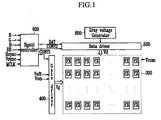
- a liquid crystal display according to an exemplary embodiment of the present invention will be described in detail with reference to FIGS. 1 and 2 .
- FIG. 1 is a block diagram of a liquid crystal display according to an exemplary embodiment of the present invention
- FIG. 2 is an equivalent circuit diagram of two subpixels of a liquid crystal display according to an exemplary embodiment of the present invention.
- the liquid crystal display includes a liquid crystal panel assembly 300, a gate driver 400 and a data driver 500 that are connected thereto, a gray voltage generator 800 that is connected to the data driver 500, and a signal controller 600 that controls them.
- the liquid crystal panel assembly 300 includes a plurality of signal lines (not shown) and a plurality of pixels PX that are connected thereto and arranged in approximately a matrix.
- the liquid crystal panel assembly 300 includes lower and upper panels 100 and 200 that are opposite each other, and a liquid crystal layer 3 that is disposed therebetween.
- the signal lines include a plurality of gate lines (not shown) that transfer gate signals (scanning signals) and a plurality of data lines (not shown) that transfer data signals.
- the gate lines extend in approximately a row direction and are almost parallel to each other, and the data lines extend in approximately a column direction and are almost parallel to each other.
- Each pixel PX includes a pair of subpixels, and each subpixel includes liquid crystal capacitors Clca and Clcb. At least one of two subpixels includes a switching element (not shown) that is connected to the gate line, the data line, and the liquid crystal capacitors Clca and Clcb.
- the liquid crystal capacitors Clca and Clcb have subpixel electrodes PEa and PEb on the lower panel 100 and a common electrode CE on the upper panel 200 as two terminals, and the liquid crystal layer 3 between the subpixel electrodes PEa and PEb and the common electrode CE functions as a dielectric material.
- a pair of subpixel electrodes PEa and PEb are separated from each other and constitute one pixel electrode PE.
- the common electrode CE is formed on an entire surface of the upper panel 200 and receives a common voltage Vcom.
- the liquid crystal layer 3 has a negative dielectric anisotropy, and liquid crystal molecules of the liquid crystal layer 3 may be aligned so that long axes thereof are perpendicular to a surface of the two display panels when there is no electric field.
- a color display is represented by allowing each pixel PX to inherently display one of the primary colors (spatial division) or to sequentially display the primary colors (temporal division).
- a desired color is determined by the spatial or temporal sum of the primary colors.
- An example of a set of the primary colors includes red, green, and blue.
- FIG. 2 shows as an example of spatial division in which each pixel PX is provided with a color filter CF for displaying one of the primary colors in a region of the upper panel 200.
- the color filter CF may be formed on or under the subpixel electrodes PEa and PEb of the lower panel 100.
- a polarizer (not shown) is provided in the outer surface of each of the display panels 100 and 200. Polarization axes of each polarizers may be orthogonal. In a reflective liquid crystal display, one of the two polarizers is optional. An orthogonal polarizer blocks incident light entering the liquid crystal layer 3 where there is no electric field.
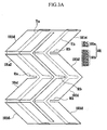
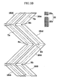
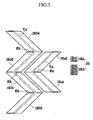
- a pixel electrode, a common electrode, and a color filter of a liquid crystal panel assembly will be described with reference to FIGS. 3A , 3B , 4 , 5 , 6A, 6B , 7A , and 7B .
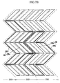
- FIGS. 3A to 4 are layout views of a pixel electrode and a common electrode in a liquid crystal panel assembly according to exemplary embodiments of the present invention
- FIGS. 6A to 6C are top plan views of a basic electrode piece of each subpixel electrode shown in FIGS. 3A to 5
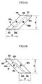
- FIGS. 7A and 7B are schematic layout views of a liquid crystal panel assembly not according to the invention including a plurality of pixel electrodes shown in FIG. 5 .
- each pixel electrode 191 includes a pair of first and second subpixel electrodes 191a and 191b that are separated from each other.
- a first subpixel electrode 191a and a second subpixel electrode 191b are adjacently disposed in a row direction and have cutouts 91a and 91b, respectively.
- the common electrode 270 (see FIG. 2 ) has cutouts 71a, 71b, 71b1, 71b2, and 71b3 that are opposite to the first and second subpixel electrodes 191a and 191b.
- the first subpixel electrode 191 a and the second subpixel electrode 191 b constituting one pixel electrode 191, may be connected to different switching elements (not shown).
- the first subpixel electrode 191a may be connected to a switching element (not shown) and the second subpixel electrode 191b may be coupled to the first subpixel electrode 191a through capacitive coupling.
- Each of the first and second subpixel electrodes 191a and 191 b includes at least one parallelogram electrode piece 196 shown in FIG. 6A and at least one parallelogram electrode piece 197 shown in FIG. 6B .
- each of the subpixel electrodes 191a and 191b forms part of the basic electrode 198.
- each of the electrode pieces 196 and 197 has a pair of oblique edges 196o and 197o and a pair of transverse edges 196t and 197t, and has a parallelogram shape.
- Each of the oblique edges 1960 and 1970 forms an oblique angle to the transverse edges 196t and 197t, and a size of the oblique angle may be about 45° to 135°.
- a length of the transverse edges 196t and 197t i.e., a width W
- a distance between the transverse edges 196t and 197t i.e., a height H
- the cutouts 61 and 62 facing the electrode pieces 196 and 197 are formed in the common electrode 270, and the electrode pieces 196 and 197 are divided into two subregions S 1 and S2 about the cutouts 61 and 62.
- the cutouts 61 and 62 include oblique portions 61o and 62o in parallel to the oblique edges 196o and 197o of the electrode pieces 196 and 197, and transverse portions 61t and 62t that overlap with the transverse edges 196t and 197t of the electrode pieces 196 and 197 while forming an obtuse angle with the oblique portions 61o and 62o.
- Each of the subregions S 1 and S2 has two primary edges that are defined by the oblique portions 61o and 62o of the cutouts 61 and 62 and the oblique edges 196o and 197o of the electrode pieces 196 and 197.
- a distance between primary edges, i.e., a width of a subregion, may be about 25 to 40 ⁇ m.
- a basic electrode 198 shown in FIG. 6C is formed by coupling of the right-inclination electrode piece 196 and the left-inclination electrode piece 197.
- An angle at which the right-inclination electrode piece 196 and the left-inclination electrode piece 197 are formed may be approximately a right angle, and the two electrode pieces 196 and 197 may be partly connected.
- Non-connected portions constitute a cutout 90, and are positioned in a concave side. However, the cutout 90 is optional.
- the outside transverse edges 196t and 197t of electrode pieces 196 and 197 constitute the transverse edge 198t of the basic electrode 198, and the corresponding oblique edges 196o and 197o of electrode pieces 196 and 197 are connected to each other to form curved edges 198o1 and 198o2 of the basic electrode 198.
- the curved edges 198o1 and 198o2 include a convex edge 198o1 that meets with an obtuse angle, for example about 135° with the transverse edge 198t, and a concave edge 198o2 that meets with an acute angle, for example about 45° with the transverse edge 198t.
- the curved edges 198o1 and 198o2 are formed as a pair of oblique edges 196o and 197o and meet with approximately a right angle, and a curved angle thereof is approximately a right angle.
- the cutout 60 may extend to approximately the center of the basic electrode 198 toward a convex summit VV on the convex edge 198o1 from a concave summit CV on the concave edge 198o2. Furthermore, the cutouts 61 and 62 of the common electrode 270 are connected to each other to form the cutout 60. Transverse portions 61t and 62t that overlap in the cutouts 61 and 62 are added to constitute one transverse portion 60t1.
- the cutout 60 includes a curved portion 60o that has a curved point CP, a central transverse portion 60t1 that is connected to the curved point CP of the curved portion 60o, and a pair of vertical transverse portions 60t2 that are connected to both ends of the curved portion 60o.
- the curved portion 60o of the cutout 60 includes a pair of oblique portions that meet with a right angle, is almost parallel to the curved edges 198o1 and 198o2 of the basic electrode 198, and divides the basic electrode 198 into a left half and a right half.
- the central transverse portion 60t1 of the cutout 60 forms an obtuse angle, for example about 135° with the curved portion 60o, and extends toward a convex summit VV of the basic electrode 198.
- the vertical transverse portion 60t2 is aligned with the transverse edge 198t of the basic electrode 198 and forms an obtuse angle, for example about 135° with the curved portion 60o.
- the basic electrode 198 and the cutout 60 are in an approximate inversion symmetry about an imaginary straight line (hereinafter, referred to as a "transverse center line") connecting the convex summit VV and the concave summit CV of the basic electrode 198.
- a size of the first subpixel electrode 191a is smaller than that of the second subpixel electrode 191b.
- a height of the second subpixel electrode 191b is larger than that of the first subpixel electrode 191a, and widths of subpixel electrodes 191a and 191b are substantially equal.
- the number of electrode pieces of the second subpixel electrode 191b is larger than that of the electrode pieces of the first subpixel electrode 191a.
- the first subpixel electrode 191a includes a left-inclination electrode piece 197 and a right-inclination electrode piece 196, and has substantially the same structure as a basic electrode 198 shown in FIG. 6C .
- the second subpixel electrode 191b includes the combination of at least two left-inclination electrode pieces 197, at least two right-inclination electrode pieces 196, the basic electrode 198 shown in FIG. 6C , and the left and right inclination electrode pieces 196 and 197 that are coupled thereto.
- the second subpixel electrode 191b shown in FIGS. 3A and 3B includes six electrode pieces 191b1 to 191b6, and two electrode pieces 191b5 and 191b6 among them are disposed in an upper part and a lower part of the first subpixel electrode 191a.
- An aperture ratio is increased as a transverse portion is formed by adding the transverse portions 61t and 62t of the cutouts 61 and 62 of the common electrode 270 to a place adjacent to electrode pieces 191a1 and 191a2 of the first subpixel electrode 191a and electrode pieces 191b5 and 191b6 of the second subpixel electrode 191 b.
- a height of electrode pieces 191a1, 191a2, 191b1, and 191b2 that are disposed in the middle of the structure and that of electrode pieces 191 b3 to 191 b6 that are disposed in the upper and lower part of the structure are substantially the same, but in a structure shown in FIG. 3B , a height of the middle electrode pieces 191a1, 191a2, 191b1, and 191b2 and that of the upper and lower electrode pieces 191b3 to 191b6 are different from each other.
- a height of the upper and lower electrode pieces 191b3 to 191b6 is about half that of the middle electrode pieces 191a1, 191a2, 191b1, and 191b2. Accordingly, an area ratio of the first subpixel electrode 191a and the second subpixel electrode 191b is approximately 1:2.
- an area ratio of the first subpixel electrode 191a and the second subpixel electrode 191b is approximately 1:3.
- a height of the middle electrode pieces 191a1, 191a2, 191b1, and 191b2 may be 1 to 2.5 times that of the upper and lower electrode pieces 191b3 to 191b6.
- a desired area ratio can be obtained if a height of the upper and lower electrode pieces 191b3 to 191b6 is adjusted in this way, and an area ratio of approximately 1:3 to 1:1.1 is preferred.
- the second subpixel electrode 191b shown in FIG.4 includes four electrode pieces 191b1 to 191b4, and two electrode pieces 191b3 and 191b4 among them are disposed in an upper part and a lower part of the first subpixel electrode 191 a.
- a height of electrode pieces 191b3 and 191b4 that are disposed in an upper part and a lower part of the first subpixel electrode 191a is smaller than that of electrode pieces 191b1 and 191 b2 that are disposed in a side surface of the first subpixel electrode 191a, and a height ratio thereof is, for example, about 1:2.
- An area ratio of the first subpixel electrode 191 a and the second subpixel electrode 191b can be adjusted by adjusting heights of four electrode pieces 191b1 to 191b4.
- the second subpixel electrode 191b not according to the invention shown in FIG. 5 includes four electrode pieces 191b1 to 191b4, and has a three-time curved structure.
- An area ratio can be adjusted by adjusting heights of the electrode pieces 191a1, 19 1 a2, and 191b1 to 191b4.
- shapes of adjacent pixel electrodes 191 in a row direction are substantially equal to each other and a transverse center line of each of pixel electrodes 191 is in substantially the same straight line, and adjacent pixel electrodes 191 in a column direction are in lateral inversion symmetry with each other.
- Red, green, and blue color filters 230R, 230G, and 230B extend along adjacent pixel electrodes 191 in a column direction.
- transverse center lines of adjacent pixel electrodes 191 in a row direction are unmatched.
- a transverse center line of a left pixel electrode 191 and an upper transverse edge of the first subpixel electrode 191 a of a right pixel electrode 191 are in substantially the same straight line.
- first subpixel electrode 191a is in the left side and the second subpixel electrode 191b is in the right side, lateral dispositions thereof are substantially equal to each other, but the first subpixel electrode 191a and the second subpixel electrode 191b are in inversion symmetry with each other.
- Adjacent pixel electrodes 191 in a column direction are in lateral inversion symmetry to each other.
- Red, green, and blue color filters 230R, 230G, and 230B extend along adjacent pixel electrodes 191 in a column direction.
- the positional relationship of the pixel electrodes 191 can be changed, and neighboring pixel electrodes 191 in a row or column direction can be disposed to be unmatched in other manners.
- a gray voltage generator 800 generates a plurality of gray voltages (or a reference gray voltage) related to transmittance of a pixel PX.
- the gate driver 400 is connected to a gate line of the liquid crystal panel assembly 300 to apply a gate signal Vg comprising the combination of a gate-on voltage Von and a gate-off voltage Voffto the gate line.
- the data driver 500 is connected to the data line of the liquid crystal panel assembly 300, selects a gray voltage from the gray voltage generator 800, and applies the gray voltage as a data signal to the data line.
- the data driver 500 when the gray voltage generator 800 provides only a predetermined number of reference gray voltages rather than all voltages for all grays, the data driver 500 generates gray voltages for all grays by dividing the reference gray voltage and selects a data signal among them.
- the signal controller 600 controls the gate driver 400, the data driver 500, etc.
- Each of the driving devices 400, 500, 600, and 800 may be directly mounted on the liquid crystal panel assembly 300 in a form of at least one IC chip, mounted on flexible printed circuit film (not shown) to attach to the liquid crystal panel assembly 300 in a tape carrier package (TCP), or mounted on a separate printed circuit board (PCB) (not shown).
- TCP tape carrier package
- PCB separate printed circuit board
- the driving devices 400, 500, 600, and 800 may be integrated with the liquid crystal panel assembly 300.
- the driving devices 400, 500, 600, and 800 may be integrated in a single chip, and at least one of these devices or at least one circuit element of these devices may be disposed outside of a single chip.
- the signal controller 600 receives input image signals R, G, and B and an input control signal for controlling the display of the signals from an external graphics controller (not shown).
- the input control signal includes, for example, a vertical synchronization signal Vsync, a horizontal synchronizing signal Hsync, a main clock signal MCLK, and a data enable signal DE.
- the signal controller 600 appropriately processes input image signals R, G, and B to correspond to an operating condition of the liquid crystal panel assembly 300 and the data driver 500 based on input image signals R, G, and B and input control signals, generates a gate control signal CONT1 and a data control signal CONT2, then transfers the gate control signal CONT1 to the gate driver 400 and outputs the data control signal CONT2 and the processed image signal DAT to the data driver 500.
- the output image signal DAT is output as a digital signal and has a predetermined value (or gray).
- the gate control signal CONT1 includes a scanning start signal STV for instructing the start of scanning, and at least one clock signal for controlling an output period of a gate-on voltage Von.
- the gate control signal CONT1 may further include an output enable signal OE for limiting a duration time of the gate-on voltage Von.
- the data control signal CONT2 includes a horizontal synchronization start signal STH indicating the start of the transfer of image data for one set of subpixels, and a load signal LOAD and a data clock signal HCLK for applying a data signal to the liquid crystal panel assembly 300.
- the data control signal CONT2 may further include an inversion signal RVS for inverting the voltage polarity of a data signal for a common voltage Vcom (hereinafter, "voltage polarity of a data signal for a common voltage” is briefly referred to as “polarity of a data signal”).
- Vcom voltage polarity of a data signal for a common voltage
- the data driver 500 receives digital image signals DAT for one set of subpixels and selects a gray voltage corresponding to each digital image signal DAT, depending on the data control signal CONT2 from the signal controller 600, the digital image signal DAT is converted to an analog data signal and then the signal is applied to a corresponding data line.
- the gate driver 400 turns on the switching element that is connected to the gate lines by applying the gate-on voltage Von to the gate lines depending on the gate control signal CONT1 from the signal controller 600.
- a data signal that is applied to the data lines is applied to a corresponding subpixel PX through the turned-on switching element.
- each subpixel may receive a separate data voltage through the same data line at different times or receive a separate data voltage through a different data line at the same time.
- first subpixel electrode 191a when the first subpixel electrode 191a is connected to a switching element (not shown) and the second subpixel electrode 191b is coupled to the first subpixel electrode 191a through capacitive coupling, only a subpixel including the first subpixel electrode 191a may receive a data voltage through a switching element, and a subpixel including the second subpixel electrode 191b may have a voltage that changes depending on the change of a voltage of the first subpixel electrode 191a.
- a voltage of the first subpixel electrode 191 a having a relatively small area is higher than that of the second subpixel electrode 191 b having a relatively large area.
- a pixel electrode 191 and a common electrode 270 are referred to as "field generating electrodes.”
- Liquid crystal molecules of the liquid crystal layer 3 are arranged so that a long axis thereof is perpendicular to a direction of an electric field in response to an electric field, and the degree of polarization of light incident to the liquid crystal layer 3 changes depending on an inclination angle of the liquid crystal molecules.
- the change in polarization is represented by a change oftransmittance by a polarizer, whereby a liquid crystal display displays an image.
- An inclination angle of the liquid crystal molecules changes depending on the intensity of an electric field. Since voltages of two liquid crystal capacitors Clca and Clcb are different from each other, an inclination angle of the liquid crystal molecules changes, whereby luminance of two subpixels is changed.
- a side gamma curve can be more similar to a front gamma curve.
- An inclination direction of the liquid crystal molecules is firstly determined by a horizontal component that is generated by distorting a varying main electric field of subpixel electrodes 191a and 191b and cutouts 71a, 71b, 71b1, 71b2, 91a, 91b, and 92b of the field generating electrodes 191 and 270.
- a horizontal component of the main electric field is almost perpendicular to an edge of the cutouts 71a, 71b, 71b1, 71b2, 91a, 91b, and 92b and an edge of the subpixel electrodes 191a and 191b.
- most liquid crystal molecules on each subregion that is divided by the cutouts 71a, 71b, 71b1, 71b2, 91a, 91b, and 92b are arranged in a direction perpendicular to a primary edge.
- a direction of a secondary electric field that is secondarily generated by the voltage difference between the subpixel electrodes 191 a and 191b is perpendicular to a primary edge of a subregion.
- a direction of a secondary electric field agrees with a direction of a horizontal component of a main electric field.
- a secondary electric field between the subpixel electrodes 191a and 191b functions to enhance the determination of an inclination direction of liquid crystal molecules.
- a data signal is applied to all pixels PX, so that an image of one frame is displayed.
- a state of an inversion signal RVS that is applied to the data driver 500 is controlled so that a next frame starts when one frame ends, and the polarity of a data signal that is applied to each pixel PX is opposite to the polarity in a previous frame ("frame inversion").
- the polarity of a data signal flowing through one data line may be changed (e.g., row inversion and dot inversion) or the polarity of the data signals that are applied to one set of pixels may be different from each other (e.g., column inversion and dot inversion).
- a liquid crystal panel assembly according to an exemplary embodiment of the present invention will be described in detail with reference to FIGS. 1 , 2 , 4A , 6 , and 8 to 12 .
- FIG. 8 is an equivalent circuit diagram of a pixel of a liquid crystal panel assembly according to an exemplary embodiment of the present invention.
- the liquid crystal panel assembly includes a signal line including a plurality of pairs of gate lines GLa and GLb, a plurality of data lines DL, and a plurality of storage electrode lines SL and a plurality of pixels PX that are connected thereto.
- Each pixel PX includes a pair of subpixels PXa and PXb, and the respective subpixels PXa and PXb include switching elements Qa and Qb that are connected to corresponding gate lines GLa and GLb and data lines DL, liquid crystal capacitors Clca and Clcb that are connected thereto, and storage capacitors Csta and Cstb that are connected to the switching elements Qa and Qb and the storage electrode lines SL.
- the switching elements Qa and Qb are three terminal elements such as a thin film transistor that are provided in the lower panel 100.
- a control terminal thereof is connected to the gate lines GLa and GLb, an input terminal thereof is connected to the data line DL, and an output terminal thereof is connected to the liquid crystal capacitors Clca and Clcb and the storage capacitors Csta and Cstb.
- the storage capacitors Csta and Cstb assist the liquid crystal capacitors Clca and Clcb and are formed with the overlap of a storage electrode line SL and a pixel electrode PE that are provided in the lower panel 100 with an insulator interposed therebetween.
- a predetermined voltage such as a common voltage Vcom is applied to the storage electrode line SL.
- the storage capacitors Csta and Cstb may be formed with the overlap of the subpixel electrodes PEa and PEb and a previous gate line directly on the subpixel electrodes PEa and PEb via an insulator.
- the signal controller 600 can receive input image signals R, G, and B for one pixel PX, convert the signals to an output image signal DAT for subpixels PXa and PXb, and transmit the signals to the data driver 500.
- the gray voltage generator 800 by separately making a gray voltage set for subpixels PXa and PXb, providing them to the data driver 500 or selecting them in the data driver 500, a different voltage can be applied to the two subpixels PXa and PXb.
- composition gamma curve in the front is adjusted to agree with a reference gamma curve in the front to be most suitable for the liquid crystal panel assembly, and a composition gamma curve in the side is adjusted to be most similar to the reference gamma curve in the front.
- FIG. 8 An example of the liquid crystal panel assembly shown in FIG. 8 will be described in detail with reference to FIGS. 3B , 9 , and 10 .
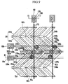
- FIG. 9 is a layout view of a liquid crystal panel assembly according to an exemplary embodiment of the present invention
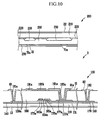
- FIG. 10 is a cross-sectional view of a liquid crystal panel assembly taken along line X-X'-X" of FIG. 9 .
- the liquid crystal panel assembly includes a lower panel 100 and an upper panel 200 that are opposite to each other, and a liquid crystal layer 3 therebetween.
- a plurality of gate conductors including a plurality of pairs of first and second gate lines 121 a and 121 b and a plurality of storage electrode lines 131 are formed on the insulation substrate 110.
- the insulation substrate 110 may be made of for example transparent glass, or plastic.
- the first and second gate lines 121 a and 121 b transfer a gate signal, and extend mainly in a horizontal direction and are positioned in the lower side and the upper side, respectively.
- the first gate line 121a includes a wide end part 129a for connecting a plurality of first gate electrodes 124a that protrude to the upper side, to other layers or the gate driver 400.
- the second gate line 121b includes a wide end part 129b for connecting a plurality of second gate electrodes 124a that protrude to the lower side, to other layers or the gate driver 400.
- the gate lines 121a and 121 b are extended to directly connect thereto.
- the storage electrode line 131 receives a predetermined voltage such as a common voltage Vcom, and extend mainly in a horizontal direction.
- Each of the storage electrode lines 131 is positioned between the first gate line 121a and the second gate line 121b, and maintains an almost equal distance from gate lines 121a and 121b.
- Each storage electrode line 131 includes a plurality of pairs of first and second storage electrodes 137a and 137b that are vertically extended.
- the shape and disposition of the storage electrodes 137a and 137b and the storage electrode line 131 may be variously changed.
- the gate conductors 121a, 121b, and 131 may be made of metals such as aluminum (Al), silver (Ag), copper (Cu), molybdenum (Mo), chromium (Cr), thallium (Ta), titanium (Ti), and/or alloys thereof.
- the gate conductors 121a, 121b, and 131 may also have a multilayer structure including two conductive layers (not shown) that have different physical properties.
- One conductor layer among them may be made of a metal having low resistivity, for example, aluminum metals, silver metals, or copper metals, thereby reducing signal delay or voltage drop.
- the other conductor layer may be made of a metal having Mo, Cr, Ta, Ti and/or a material having good physical, chemical, and electrical contact characteristics with other materials, such as ITO (indium tin oxide) and IZO (indium zinc oxide).
- ITO indium tin oxide
- IZO indium zinc oxide
- An example of such a combination may include a chromium lower layer and an aluminum (alloy) upper layer, and an aluminum (alloy) lower layer and a molybdenum (alloy) upper layer.
- the gate conductors 121a, 121b, and 131 may made of other various metals or electrical conductors.
- a gate insulating layer 140 which is made of materials such as, for example, silicon nitride SiNx, or silicon oxide SiOx, is formed on the gate conductors 121a, 121b, and 131.
- a plurality of first and second semiconductor islands 154a and 154b which are made of materials such as, for example hydrogenated amorphous silicon (a-Si), or polysilicon, are formed on the gate insulating layer 140.
- the first and second semiconductors 154a and 154b are positioned on the first and second gate electrodes 124a and 124b, respectively.
- a pair of ohmic contact islands 163a and 165a are formed on each of the first semiconductors 154a, and a pair of ohmic contact islands (not shown) are formed on each of the second semiconductors 154b.
- the ohmic contact islands 163a and 165a may be made of a material such as n+ hydrogenated amorphous silicon in which an n-type impurity such as phosphorus is doped with a high concentration, or silicide.
- a data conductor including a plurality of data lines 171 and a plurality of pairs of first and second drain electrodes 175a and 175b is formed on the ohmic contacts 163a and 165a and the gate insulating layer 140.
- Each of the data lines 171 transfers a data signal, and extends in a vertical direction to intersect the gate lines 121 a and 121 b and the storage electrode line 131.
- Each of the data lines 171 includes a wide end part 179 for connecting a plurality of pairs of first and second source electrodes 173a and 173b that extend toward the first and second gate electrodes 124a and 124b to other layers or the data driver 500.
- the data lines 171 extend to directly connect thereto.
- the first and second drain electrodes 175a and 175b are separated from each other and are also separated from each of the data lines 171.
- the first and second drain electrodes 175a and 175b face the first and second source electrodes 173a and 173b about the first and second gate electrode 124a and 124b, and each includes wide end parts 177a and 177b and a bar shaped end part.
- the wide end parts 177a and 177b are overlapped with the first and second storage electrodes 137a and 137b, respectively, and a part of the bar shaped end part is surrounded by the curved first and second source electrodes 173a and 173b.
- the first and second gate electrodes 124a and 124b, the first and second source electrodes 173a and 173b, the first and second drain electrodes 175a and 175b, and the first and second semiconductors 154a and 154 constitute first and second thin film transistors TFT Qa and Qb.
- a channel of the first and second thin film transistors is formed in the first and second semiconductors 154a and 154b between the first and second source electrodes 173a and 173b and the first and second drain electrodes 175a and 175b.
- Data conductors 171, 175a, and 175b may be made of a refractory metal such as molybdenum, chromium, tantalum, and titanium, or their alloys.
- the data conductors 171, 175a, and 175b may have a multilayer structure including a refractory metal layer (not shown) and a low resistance conductive layer (not shown).
- a multilayer structure includes, for example, a dual-layer of a chromium or molybdenum (alloy) lower layer and an aluminum (alloy) upper layer, and a triple-layer of a molybdenum (alloy) lower layer, an aluminum (alloy) middle layer, and a molybdenum (alloy) upper layer.
- the data conductors 171, 175a, and 175b may be made of other various metals or conductors.
- Side surfaces of the data conductors 171, 175a, and 175b may be inclined to the surface of the substrate 110, and an inclination angle thereof may be about 30° to 80°.
- the ohmic contact islands 163a and 165a are present between the semiconductors 154a and 154b in a lower part thereof and the data conductors 171, 175a, and 175b in an upper part thereof, and reduce contact resistance between them.
- the semiconductors 154a and 154b have a portion that is exposed without being covered by the data conductors 171, 175a, and 175b, and a portion between the source electrodes 173a and 173b and the drain electrodes 175a and 175b.
- a passivation layer 180 is formed on the data conductors 171, 175a, and 175b and the exposed portion of the semiconductors 154a and 154b.
- the passivation layer 180 may be made of materials such as an inorganic insulator, or an organic insulator, and may have a flat surface.
- the organic insulator may have a dielectric constant of 4.0 or less, and may have photosensitivity.
- the passivation layer 180 may also have a dual-layer structure of a lower inorganic layer and an upper organic layer so as not to cause damage in the exposed portion of the semiconductors 154a and 154b maintaining the desirable insulating characteristics of the organic layer.
- a plurality of contact holes 182, 185a, and 185b for exposing the end part 179 of the data lines 171 and the wide end parts 177a and 177b of the first and second drain electrodes 175a and 175b are formed in the passivation layer 180.
- a plurality of contact holes 181 a and 181b for exposing the end parts 129a and 129b of the gate lines 121a and 121b are formed in the passivation layer 180 and the gate insulating layer 140.
- a plurality of pixel electrodes 191 and a plurality of contact assistants 81a, 81b, and 82 are formed on the passivation layer 180.
- the pixel electrodes 191 may be made of a transparent conductive material such as ITO or IZO, or a reflective metal such as aluminum, silver, chromium, or their alloys.
- Each of the pixel electrodes 191 includes the first and second subpixel electrodes 191 a and 191b, and each of the subpixel electrodes 191 a and 191 b has cutouts 91 a and 91b.
- the storage electrode line 131, the extensions 177a and 177b of the drain electrodes 175a and 175b, and the contact holes 185a and 185b are positioned at a transverse center line of the subpixel electrodes 191a and 191 b.
- a straight line that connects a curved point of subpixel electrodes 191a and 191b is the border of a subregion described above, and at this part, arrangement of liquid crystal molecules is scattered, thereby generating texture.
- the disposition can allow an aperture ratio to improve while not exposing texture.
- a length in which each of the data lines 171 is overlaps with a first subpixel electrode 191 a of one pixel electrode 191 and a length in which each of the data linse 171 overlaps with a neighboring second subpixel electrode 191 b of the pixel electrode 191 may be substantially equal to each other.
- the first and second subpixel electrodes 191a and 191b are connected to the first and second drain electrodes 175a and 175b through the contact holes 185a and 185b.
- the first and second subpixel electrodes 191 a and 191 b, a common electrode 270 of the upper panel 200, and the liquid crystal layer 3 therebetween constitute first and second liquid crystal capacitors Clca and Clcb, and the first and second subpixel electrodes 191a and 191b and the common electrode 270 maintain an applied voltage even after the thin film transistors Qa and Qb are turned off.
- the first and second storage capacitors Csta and Cstb enhance voltage storage ability of the first and second liquid crystal capacitors Clca and Clcb.
- the contact assistants 81 a, 81 b, and 82 are connected to end parts 129a and 129b of the gate line 121 and an end part 179 of each of the data lines 171 through the contact holes 181a, 181b, and 182, respectively.
- the contact assistants 81 a, 81 b, and 82 support adhesion between the end parts 129a and 129b of the gate lines 121a and 121 b and the end part 179 of each of the data lines 171 and an external apparatus, and protect them.
- a light blocking member 220 is formed on the insulation substrate 210 and may be made of a material such as transparent glass, or plastic.
- the light blocking member 220 includes a curved portion corresponding to the curved edge of the pixel electrode 191 and a quadrangle portion corresponding to a thin film transistor, prevents light leakage between the pixel electrodes 191, and defines a region that is opposite to the pixel electrode 191.
- a plurality of color filters 230 are formed on the substrate 210 and the light blocking member 220.
- the color filters 230 are present within a region that is surrounded by the light blocking member 230, and extend long along a column of the pixel electrode 191.
- Each of the color filters 230 can display one of three primary colors such as red, green, and blue.
- An overcoat 250 is formed on each of the color filters 230 and the light blocking member 220.
- the overcoat 250 may be made of an (organic) insulating material, preventing each of the color filters 230 from being exposed, and providing a flat surface.
- the overcoat 250 is optional.
- a common electrode 270 may be formed on the overcoat 250.
- the common electrode 270 may be made of a transparent conductor such as ITO, or IZO and have a plurality of cutouts 71a and 71b.
- the number of cutouts 71a and 71b may be changed depending on design elements. As the light blocking member 220 overlaps with the cutouts 71a and 71b, they can block light leakage around the cutouts 71a and 71b.
- Alignment layers 11 and 21 are formed on an inner surface of the display panels 100 and 200, and may be vertical alignment layers.
- Polarizers 12 and 22 are provided in the outer surface of the display panels 100 and 200. Polarization axes of two polarizers 12 and 22 may be orthogonal and a single polarization axis among them may be parallel to the gate lines 121a and 121b. In a reflective liquid crystal display, one of two polarizers 12 and 22 is optional.
- a liquid crystal display may include polarizers 12 and 22, a phase delay layer, display panels 100 and 200, and a backlight unit (not shown) for supplying light to the liquid crystal layer 3.
- the liquid crystal layer 3 has negative dielectric anisotropy, and liquid crystal molecules of the liquid crystal layer 3 are aligned so that long axes thereof are perpendicular to a surface of the two display panels in a state where there is no electric field.
- the cutouts 71 a and 71b may be replaced with a protrusion (not shown) or a depression (not shown).
- the protrusion may be made of an organic material or an inorganic material, and may be disposed on or under the field generating electrodes 191 and 270.
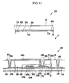
- FIG. 11 is a layout view of a liquid crystal panel assembly not according to the present invention
- FIG. 12 is a cross-sectional view of a liquid crystal panel assembly taken along line XII-XII'-XII" of FIG. 11 .
- the liquid crystal panel assembly includes a lower panel 100, an upper panel 200, and a liquid crystal layer 3 therebetween.
- a layered structure of the liquid crystal panel assembly is substantially the same as the layered structure of the liquid crystal panel assembly shown in FIGS. 9 and 10 .
- a gate conductor including a plurality of pairs of first and second gate lines 121 a and 121b and a plurality of storage electrode lines 131 is formed on the insulation substrate 110.
- the first and second gate lines 121a and 121b include the first and second gate electrodes 124a and 124b and end parts 129a and 129b, respectively.
- a gate insulating layer 140 is formed on the gate conductors 121a, 121b, and 131.
- a plurality of semiconductors 154a and 154b are formed on the gate insulating layer 140, and a plurality of ohmic contacts 163b and 165b are formed thereon.
- a data conductor including a plurality of data lines 171 and a plurality of first and second drain electrodes 175a and 175b is formed on the ohmic contacts 163b and 165b.
- Each of the data lines 171 includes a plurality of first and second source electrodes 173a and 173b and an end part 179, and the drain electrodes 175a and 175b include wide end parts 177a and 177b.
- a passivation layer 180 is formed on the data conductors 171, 175a, and 175b and the exposed parts of the semiconductors 154a and 154b.
- a plurality of contact holes 181a, 181b, 182, 185a, and 185b are formed on the passivation layer 180 and the gate insulating layer 140.
- a plurality of pixel electrodes 191 including the first and second subpixel electrodes 191a and 191b and a plurality of contact assistants 81a, 81b, and 82 are formed on the passivation layer 180, and cutouts 91a and 91b are formed in the first and second subpixel electrodes 191a and 191b, respectively.
- An alignment layer 11 is formed on the pixel electrodes 191, the contact assistants 81a, 81b, and 82, and the passivation layer 180.
- a light blocking member 220, a common electrode 270 having cutouts 71 a and 71b, and an alignment layer 21 are formed on the insulation substrate 210.
- a vertical position of the first and second gate lines 121a and 121b is opposite thereto, and thus a lateral position of the first and second thin film transistors Qa and Qb is opposite about each of the data lines 171.
- the first and second storage electrodes 137a and 137b are also positioned in the right side and the left side about the data lines 171.
- An area of the second storage electrode 137b is larger than that of the first storage electrode 137a and the former is about two times that of the latter.
- a wide end part 177b of the second drain electrode 175b has a larger area than a wide end part 177a of the first drain electrode 175a, and the former is about two times that of the latter.
- Each of the color filters 230 extend in a vertical direction while being periodically covered along a column of the pixel electrodes 191, and do not exist in a peripheral area of the end parts 129a and 129b of the gate lines 121a and 121b and the end part 179 of the data line 171.
- a penetrating hole 235 that passes the contact hole 185b and that is larger than the contact hole 185b is formed in the color filters 230.
- a neighboring one of the color filters 230 may function as a light blocking member for blocking leaking light between neighboring pixel electrodes 191 by overlapping the data lines 171, making the light blocking member of the upper panel 200 optional.
- a passivation layer (not shown) may be provided under the color filters 230.
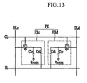
- a liquid crystal panel assembly according to an exemplary embodiment of the present invention will be described in detail with reference to FIGS. 1 , 2 , 3B , and 13 to 15 .
- FIG. 13 is an equivalent circuit diagram of a pixel of a liquid crystal panel assembly according to an exemplary embodiment of the present invention.
- the liquid crystal panel assembly includes signal lines including a plurality of gate lines GL, a plurality of pairs of data lines DLc and DLd, and a plurality of storage electrode lines SL and a plurality of pixels PX that are connected thereto.
- Each pixel PX includes a pair of subpixels PXc and PXd, and the respective subpixels PXc and PXd include switching elements Qc and Qd that are connected to a corresponding gate line GL and data lines DLc and DLd, liquid crystal capacitors Clcc and Clcd that are connected thereto, and storage capacitors Cstc and Cstd that are connected to the switching elements Qc and Qd and the storage electrode line SL.
- Each of the switching elements Qa and Qb is also a three terminal element such as a thin film transistor that is provided in the lower panel 100, and a control terminal thereof is connected to the gate line GL, an input terminal thereof is connected to the data lines DLc and DLd, and an output terminal thereof is connected to the liquid crystal capacitors Clcc and Clcd and the storage capacitors Cstc and Cstd.
- Subpixels PXa and PXb constitute a pixel PX in the liquid crystal display shown in FIG. 8 sequentially receive a data voltage, but in the present exemplary embodiment, two subpixels PXc and PXd simultaneously receive a data voltage.
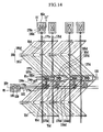
- FIG. 13 An example of the liquid crystal panel assembly shown in FIG. 13 will be described in detail with reference to FIGS. 3B , 14 , and FIG. 15 .
- FIG. 14 is a layout view of a liquid crystal panel assembly according to an exemplary embodiment of the present invention
- FIG. 15 is a cross-sectional view of the liquid crystal panel assembly taken along line XV-XV'-XV" of FIG. 14 .
- the liquid crystal panel assembly includes a lower panel 100 and an upper panel 200 that are opposite to each other, and a liquid crystal layer 3 therebetween.
- a layered structure of the liquid crystal panel assembly is substantially the same as that of the liquid crystal panel assembly shown in FIGS. 9 and 10 .
- a plurality of gate conductors including a plurality of gate lines 121 and a plurality of storage electrode lines 131 are formed on the insulation substrate 110.
- Each of the gate lines 121 includes the first and second gate electrodes 124c and 124d and an end part 129.
- a gate insulating layer 140 is formed on the gate conductors 121 and 131.
- a plurality of semiconductor stripes 151 including the first and second protrusions 154c and 154d are formed on the gate insulating layer 140, and a plurality of ohmic contact stripes 161 and a plurality of ohmic contact islands 165c having protrusions 163c are formed thereon.
- a data conductor including a plurality of pairs of first and second data lines 171 c and 171d and a plurality of first and second drain electrodes 175c and 175d is formed on the ohmic contacts 161 and 165c.
- the first and second data lines 171c and 171d include a plurality of first and second source electrodes 173c and 173d, respectively, and an end part 179c and the first and second drain electrodes 175c and 175d include protrusions 177c and 177d.
- a passivation layer 180 is formed on the data conductors 171c, 171d, 175c, and 175d and the exposed parts of the semiconductors 154c and 154d, and a plurality of contact holes 181, 182c, 182d, 185c, and 185d are formed on the passivation layer 180 and the gate insulating layer 140.
- a plurality of pixel electrodes 191 including the first and second subpixel electrodes 191 c and 191d and a plurality of contact assistants 81, 82c, and 82d are formed on the passivation layer 180, and cutouts 91c and 91d are formed in the first and second subpixel electrodes 191 c and 191 d, respectively.
- An alignment layer 11 is formed on the pixel electrode 191, the contact assistants 81, 82c, and 82d, and the passivation layer 180.
- a light blocking member 220, a common electrode 270 having a plurality of color filters 230, an overcoat 250, cutouts 71 c and 71d, and an alignment layer 21 are formed on the insulation substrate 210.
- the number of gate lines 121 is half and the number of data lines 171 c and 171d is twice, compared with the liquid crystal panel assembly shown in FIGS. 9 and 10 .
- the first and second thin film transistors Qc and Qd that are connected to the first and second subpixel electrodes 191 c and 191d constituting pixel electrode 191 are connected to the same gate line 121 and different data lines 171c and 171d.
- the first and second thin film transistors Qc and Qd are positioned in the right side of the first and second data lines 171c and 171d.
- the semiconductors 154c and 154d extend along the data line 171 and the drain electrodes 175c and 175d to constitute a semiconductor stripe 151, and the ohmic contact 163c extends along the data line 171 to constitute an ohmic contact stripe 161.
- the semiconductor stripe 151 has substantially the same flat shape as each of the data line 171s, the drain electrodes 175c and 175d, and the lower ohmic contacts 161 and 165c.
- the data lines 171 comprise a pair of lines, transmittance is considerably improved.
- a data voltage may be applied to the first and second subpixel electrodes 191c and 191d without greatly deteriorating an aperture ratio.
- a data line 171, drain electrodes 175c and 175d, a semiconductor 151, and ohmic contacts 161 and 165c are formed with one photolithography process.
- a thickness thereof changes depending on a position thereof, and the photosensitive film includes a first part and a second part, particularly in decreasing order of thickness.
- the first part is positioned in a wiring region where the data line 171 and the drain electrodes 175c and 175d are positioned, and the second part is positioned in a channel region of a thin film transistor.
- a thickness of a photosensitive film depending on position
- the methods include, for example, a method of providing a light transmitting area, a light blocking area, and a translucent area in a photomask.
- a thin film that has a slit pattern or a lattice pattern is provided in a translucent area.
- a width of a slit or an interval between slits may be smaller than the resolution of a light exposer that is used in a photolithography process.
- Another example includes a method of using a photosensitive film that can flow. After forming the photosensitive film that can flow with a normal exposure mask having only a light transmitting region and a light blocking region, a thin portion is formed by flowing the photosensitive film to a region where the photosensitive film is not present, thereby simplifying manufacturing.
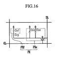
- a liquid crystal panel assembly according to an exemplary embodiment of the present invention will be described in detail with reference to the FIGS. 1 , 2 , and 16 .
- FIG. 16 is an equivalent circuit diagram of a pixel of a liquid crystal panel assembly according to an exemplary embodiment of the present invention.
- the liquid crystal panel assembly includes signal lines including a plurality of gate lines GL and a plurality of data lines DL, and a plurality of pixels PX that are connected thereto.
- Each pixel PX includes a pair of first and second subpixels PXe and PXf, and a coupling capacitor Ccp that is connected between the two subpixels PXe and PXf.
- the first subpixel PXe includes a switching element Q that is connected to the corresponding gate line GL and data line DL and a first liquid crystal capacitor Clce and a storage capacitor Cst that are connected thereto, and the second subpixel PXf includes a second liquid crystal capacitor Clcf that is connected to the coupling capacitor Ccp.
- the switching element Q is a three terminal element such as a thin film transistor that is provided in the lower panel 100, and a control terminal thereof is connected to the gate line GL, an input terminal thereof is connected to the data line DL, and an output terminal thereof is connected to the liquid crystal capacitor Clce, the storage capacitor Cste, and the coupling capacitor Ccp.
- the switching element Q applies a data voltage from a data line DL to the first liquid crystal capacitor Clce and the coupling capacitor Ccp depending on a gate signal from the gate line GL, and the coupling capacitor Ccp changes a magnitude of the voltage and transfers the voltage to the second liquid crystal capacitor Clcf.
- Vcom a common voltage Vcom is applied to the storage capacitor Cste and capacitors Clce, Cste, Clcf, and Ccp and capacitances thereof are designated by the same reference numerals
- a voltage Ve that is charged in the first liquid crystal capacitor Clce and a voltage Vf that is charged in the second liquid crystal capacitor Clcf have the following relationship.
- Vf Ve ⁇ Ccp / Ccp + Clcf
- An appropriate ratio of a voltage Ve of the first liquid crystal capacitor Clce and a voltage Vf of the second liquid crystal capacitor Clcf can be obtained by adjusting capacitance of the coupling capacitor Ccp.
Landscapes
- Physics & Mathematics (AREA)
- Nonlinear Science (AREA)
- Chemical & Material Sciences (AREA)
- Crystallography & Structural Chemistry (AREA)
- General Physics & Mathematics (AREA)
- Optics & Photonics (AREA)
- Mathematical Physics (AREA)
- Spectroscopy & Molecular Physics (AREA)
- Geometry (AREA)
- Liquid Crystal (AREA)
- Liquid Crystal Substances (AREA)
- Thin Film Transistor (AREA)
Abstract
Description
- This application claims priority to
Korean Patent Application No. 10-2005-0083265 - The present disclosure relates to a liquid crystal display.
- A liquid crystal display includes two display panels provided with field generating electrodes and a liquid crystal layer disposed between the two panels. The field generating electrodes may include a plurality of pixel electrodes and a common electrode. Voltages are applied to the field generating electrodes to generate an electric field in the liquid crystal layer. The electric field determines the orientation of liquid crystal molecules of the liquid crystal layer. These molecular orientations in turn determine the transmittance of light passing through the liquid crystal layer, thereby displaying an image by controlling polarization of incident light.
- The liquid crystal display also includes a switching element that is connected to each pixel electrode and a plurality of signal lines which include gate and data lines. A voltage may be applied to each pixel electrode through the gate and data lines by controlling the switching element.
- A liquid crystal display with a vertically aligned mode has a long axis of liquid crystal molecules arranged perpendicular to a vertical display panel. When an electric field is not applied, the liquid crystal display has a large contrast ratio and a wide reference viewing angle. An example of a wide reference viewing angle is a viewing angle in which a contrast ratio is 1:10.
- A wide viewing angle in a liquid crystal display with a vertical alignment mode may be produced by forming a cutout and a protrusion on a field generating electrode.
- Since an inclination direction of a liquid crystal molecule can be determined by a cutout and a protrusion, a reference viewing angle can be enlarged by distributing an inclination direction of the liquid crystal molecule in several directions when the cutouts and/or protrusions are used.
- Side visibility is improved by a method of adjusting transmittance by changing a voltage of two subpixels by directly applying a voltage to one subpixel and dropping a voltage through capacitive coupling in the other subpixel after dividing one pixel into two subpixels and coupling two subpixels through capacitive coupling.
- However, in this method, transmittance of the two subpixels cannot be accurately adjusted to a desired level, and light transmittance changes depending on a particular color. Further, the aperture ratio deteriorates due to the addition of a conductor for capacitive coupling, and transmittance decreases due to a voltage drop by the capacitive coupling. Moreover, because it is difficult to transmit light in a part with a protrusion or a cutout, the aperture ratio deteriorates further as the number of protrusions or cutouts increases.
- It has been suggested that aperture ratio may be increased by use of an ultra-high aperture ratio structure that enlarges a pixel electrode. However, a strong lateral field is generated around the edge of a pixel electrode because a distance between pixel electrodes is short and a distance between a pixel electrode and a data line is also short. Alignment of liquid crystal molecules is distributed due to such a lateral field, whereby texture or light leakage is generated and response time is delayed.
- Furthermore, a liquid crystal display with a vertically aligned mode has lower side visibility than front visibility. For example, in a liquid crystal display of a PVA (patterned vertically aligned) mode with a cutout, an image becomes bright towards the side, and in a serious case, a picture distorted because there is no luminance difference between high grays.
- There is a need for a liquid crystal display with improved transmittance, aperture ratio, and side visibility.
-
US 2004/0135147 A1 discloses a thin film transistor array panel, which includes an insulating substrate, a first signal wire formed on the insulating substrate, a second signal wire formed on the insulating substrate and intersecting the first signal wire in an insulating manner- First and second pixel electrodes are formed in a pixel area defined by the intersections of the first and the second signal wires. The first and second pixel electrodes include a plurality of subareas partitioned by cutouts. A direction control electrode is formed in the pixel area and includes a portion overlapping at least one of the cutouts. A first thin film transistor is connected to the direction control electrode, the first signal wire, and the second signal wire. -
US 2005/094082 A1 discloses a liquid crystal display (LCD) with a direction control electrode and a pixel electrode forming a capacitance in a pixel regions. Gate lines are formed on the first substrate and extending in the first direction. Data lines are intersecting the gate lines and each data line has a bent shape. Pixel regions are defined by the intersecting of the gate lines and the data lines. The direction control electrode is formed at the corresponding pixel region and electrically connected to the corresponding data line. The pixel electrode is formed at the corresponding pixel region and has a shape conformal to the corresponding pixel region. By adjusting the capacitance between the direction control electrode and the pixel electrode, liquid crystal stabillty is enhanced. -
EP-A-1 674 922 discloses a liquid crystal display, which includes a substrate and a pixel electrode disposed on the substrate. The pixel electrode includes a first subpixel electrode and a second subpixel electrode, wherein the first subpixel electrode includes a first electrode that includes at least two substantially parallelogram-shaped electrode pieces forming a V-shaped electrode. The second subpixel electrode includes a second electrode disposed at a position different from the first electrode, and the second electrode includes at least two substantially parallelogram shaped electrode pieces forming a V-shaped electrode. - The present invention provides a liquid crystal display according to appended claims 1-18.
- The embodiments of the present invention will become more apparent by describing in detail exemplary embodiments thereof with reference to the attached drawings, in which:
-
FIG. 1 is a block diagram of a liquid crystal display according to an exemplary embodiment of the present invention; -
FIG. 2 is an equivalent circuit diagram of two subpixels of a liquid crystal display according to an exemplary embodiment of the present invention; -
FIGS. 3A to 4 are layout views of a pixel electrode and a common electrode in a liquid crystal panel assembly according to exemplary embodiments of the present invention; -
Fig. 5 is a layout view of a pixel electrode not according to the invention; -
FIGS. 6A to 6C are top plan views of a basic electrode piece of each subpixel electrode shown inFIGS. 3A to 5 ; -
FIGS. 7A and7B are schematic layout views of a liquid crystal panel assembly including a plurality of pixel electrodes shown inFIG. 5 ; -
FIG. 8 is an equivalent circuit diagram of a pixel of a liquid crystal panel assembly according to an exemplary embodiment of the present invention; -
FIG. 9 is a layout view of a liquid crystal panel assembly according to an exemplary embodiment of the present invention; -
FIG. 10 is a cross-sectional view of a liquid crystal panel assembly taken along line X-X'-X" ofFIG. 9 ; -
FIG. 11 is a layout view of a liquid crystal panel assembly not according to the present invention; -
FIG. 12 is a cross-sectional view of a liquid crystal panel assembly taken along line XII-XII'-XII" ofFIG. 11 ; -
FIG. 13 is an equivalent circuit diagram of a pixel of a liquid crystal panel assembly according to an exemplary embodiment of the present invention; -
FIG. 14 is a layout view of a liquid crystal panel assembly according to an exemplary embodiment of the present invention; -
FIG. 15 is a cross-sectional view of a liquid crystal panel assembly taken along line XV-XV'-XV" ofFIG. 14 ; and -
FIG. 16 is an equivalent circuit diagram of a pixel of a liquid crystal panel assembly according to an exemplary embodiment of the present invention. - Hereinafter, exemplary embodiments of the present invention will be described in detail with reference to the accompanying drawings. This invention may, however, be embodied in many different forms and should not be construed as limited to the embodiments set forth herein.In the drawings, the thickness of layers, films, panels, regions, etc., are exaggerated for clarity. Like reference numerals designate like elements throughout the specification.
- A liquid crystal display according to an exemplary embodiment of the present invention will be described in detail with reference to
FIGS. 1 and2 . -
FIG. 1 is a block diagram of a liquid crystal display according to an exemplary embodiment of the present invention, andFIG. 2 is an equivalent circuit diagram of two subpixels of a liquid crystal display according to an exemplary embodiment of the present invention. - As shown in
FIG. 1 , the liquid crystal display includes a liquid crystal panel assembly 300, agate driver 400 and a data driver 500 that are connected thereto, agray voltage generator 800 that is connected to the data driver 500, and asignal controller 600 that controls them. - The liquid crystal panel assembly 300 includes a plurality of signal lines (not shown) and a plurality of pixels PX that are connected thereto and arranged in approximately a matrix.
- As shown in
FIG. 2 , the liquid crystal panel assembly 300 includes lower andupper panels liquid crystal layer 3 that is disposed therebetween. - The signal lines include a plurality of gate lines (not shown) that transfer gate signals (scanning signals) and a plurality of data lines (not shown) that transfer data signals.
- The gate lines extend in approximately a row direction and are almost parallel to each other, and the data lines extend in approximately a column direction and are almost parallel to each other.
- Each pixel PX includes a pair of subpixels, and each subpixel includes liquid crystal capacitors Clca and Clcb. At least one of two subpixels includes a switching element (not shown) that is connected to the gate line, the data line, and the liquid crystal capacitors Clca and Clcb.
- The liquid crystal capacitors Clca and Clcb have subpixel electrodes PEa and PEb on the
lower panel 100 and a common electrode CE on theupper panel 200 as two terminals, and theliquid crystal layer 3 between the subpixel electrodes PEa and PEb and the common electrode CE functions as a dielectric material. A pair of subpixel electrodes PEa and PEb are separated from each other and constitute one pixel electrode PE. The common electrode CE is formed on an entire surface of theupper panel 200 and receives a common voltage Vcom. - The
liquid crystal layer 3 has a negative dielectric anisotropy, and liquid crystal molecules of theliquid crystal layer 3 may be aligned so that long axes thereof are perpendicular to a surface of the two display panels when there is no electric field. - A color display is represented by allowing each pixel PX to inherently display one of the primary colors (spatial division) or to sequentially display the primary colors (temporal division). A desired color is determined by the spatial or temporal sum of the primary colors. An example of a set of the primary colors includes red, green, and blue.
-
FIG. 2 shows as an example of spatial division in which each pixel PX is provided with a color filter CF for displaying one of the primary colors in a region of theupper panel 200. Although not illustrated inFIG. 2 , the color filter CF may be formed on or under the subpixel electrodes PEa and PEb of thelower panel 100. - A polarizer (not shown) is provided in the outer surface of each of the
display panels liquid crystal layer 3 where there is no electric field. - A pixel electrode, a common electrode, and a color filter of a liquid crystal panel assembly will be described with reference to
FIGS. 3A ,3B ,4 ,5 ,6A, 6B ,7A , and7B . -
FIGS. 3A to 4 are layout views of a pixel electrode and a common electrode in a liquid crystal panel assembly according to exemplary embodiments of the present invention,FIGS. 6A to 6C are top plan views of a basic electrode piece of each subpixel electrode shown inFIGS. 3A to 5 .FIGS. 7A and7B are schematic layout views of a liquid crystal panel assembly not according to the invention including a plurality of pixel electrodes shown inFIG. 5 . - As shown in
FIGS. 3A to 5 , eachpixel electrode 191 includes a pair of first andsecond subpixel electrodes - A
first subpixel electrode 191a and asecond subpixel electrode 191b are adjacently disposed in a row direction and havecutouts - The common electrode 270 (see
FIG. 2 ) hascutouts second subpixel electrodes - The
first subpixel electrode 191 a and thesecond subpixel electrode 191 b constituting onepixel electrode 191, may be connected to different switching elements (not shown). - Alternatively, the
first subpixel electrode 191a may be connected to a switching element (not shown) and thesecond subpixel electrode 191b may be coupled to thefirst subpixel electrode 191a through capacitive coupling. - Each of the first and
second subpixel electrodes parallelogram electrode piece 196 shown inFIG. 6A and at least oneparallelogram electrode piece 197 shown inFIG. 6B . - When the
electrode pieces FIGS. 6A and 6B are vertically connected, they become abasic electrode 198 shown inFIG. 6C . Each of thesubpixel electrodes basic electrode 198. - As shown in
FIGS. 6A and 6B , each of theelectrode pieces transverse edges oblique edges transverse edges - It is called "right inclination" when oblique edges are inclined to the right side as in
FIG. 6A , and it is called "left inclination" when the oblique edges are inclined to the left side as inFIG. 6B . - In
electrode pieces transverse edges transverse edges - The
cutouts electrode pieces common electrode 270, and theelectrode pieces subregions S 1 and S2 about thecutouts - The
cutouts electrode pieces transverse portions transverse edges electrode pieces - Each of the subregions S 1 and S2 has two primary edges that are defined by the oblique portions 61o and 62o of the
cutouts electrode pieces - A
basic electrode 198 shown inFIG. 6C is formed by coupling of the right-inclination electrode piece 196 and the left-inclination electrode piece 197. - An angle at which the right-
inclination electrode piece 196 and the left-inclination electrode piece 197 are formed may be approximately a right angle, and the twoelectrode pieces cutout 90, and are positioned in a concave side. However, thecutout 90 is optional. - The outside
transverse edges electrode pieces transverse edge 198t of thebasic electrode 198, and the corresponding oblique edges 196o and 197o ofelectrode pieces basic electrode 198. - The curved edges 198o1 and 198o2 include a convex edge 198o1 that meets with an obtuse angle, for example about 135° with the
transverse edge 198t, and a concave edge 198o2 that meets with an acute angle, for example about 45° with thetransverse edge 198t. - The curved edges 198o1 and 198o2 are formed as a pair of oblique edges 196o and 197o and meet with approximately a right angle, and a curved angle thereof is approximately a right angle.
- The
cutout 60 may extend to approximately the center of thebasic electrode 198 toward a convex summit VV on the convex edge 198o1 from a concave summit CV on the concave edge 198o2. Furthermore, thecutouts common electrode 270 are connected to each other to form thecutout 60.Transverse portions cutouts - The
cutout 60 includes a curved portion 60o that has a curved point CP, a central transverse portion 60t1 that is connected to the curved point CP of the curved portion 60o, and a pair of vertical transverse portions 60t2 that are connected to both ends of the curved portion 60o. - The curved portion 60o of the
cutout 60 includes a pair of oblique portions that meet with a right angle, is almost parallel to the curved edges 198o1 and 198o2 of thebasic electrode 198, and divides thebasic electrode 198 into a left half and a right half. - The central transverse portion 60t1 of the
cutout 60 forms an obtuse angle, for example about 135° with the curved portion 60o, and extends toward a convex summit VV of thebasic electrode 198. - The vertical transverse portion 60t2 is aligned with the
transverse edge 198t of thebasic electrode 198 and forms an obtuse angle, for example about 135° with the curved portion 60o. - The
basic electrode 198 and thecutout 60 are in an approximate inversion symmetry about an imaginary straight line (hereinafter, referred to as a "transverse center line") connecting the convex summit VV and the concave summit CV of thebasic electrode 198. - In each
pixel electrode 191 shown inFIGS. 3A to 5 , a size of thefirst subpixel electrode 191a is smaller than that of thesecond subpixel electrode 191b. - Particularly, a height of the
second subpixel electrode 191b is larger than that of thefirst subpixel electrode 191a, and widths ofsubpixel electrodes - The number of electrode pieces of the
second subpixel electrode 191b is larger than that of the electrode pieces of thefirst subpixel electrode 191a. - The
first subpixel electrode 191a includes a left-inclination electrode piece 197 and a right-inclination electrode piece 196, and has substantially the same structure as abasic electrode 198 shown inFIG. 6C . - The
second subpixel electrode 191b includes the combination of at least two left-inclination electrode pieces 197, at least two right-inclination electrode pieces 196, thebasic electrode 198 shown inFIG. 6C , and the left and rightinclination electrode pieces - The
second subpixel electrode 191b shown inFIGS. 3A and3B includes six electrode pieces 191b1 to 191b6, and two electrode pieces 191b5 and 191b6 among them are disposed in an upper part and a lower part of thefirst subpixel electrode 191a. - An aperture ratio is increased as a transverse portion is formed by adding the
transverse portions cutouts common electrode 270 to a place adjacent to electrode pieces 191a1 and 191a2 of thefirst subpixel electrode 191a and electrode pieces 191b5 and 191b6 of thesecond subpixel electrode 191 b. - In a structure shown in
FIG. 3A , a height of electrode pieces 191a1, 191a2, 191b1, and 191b2 that are disposed in the middle of the structure and that ofelectrode pieces 191 b3 to 191 b6 that are disposed in the upper and lower part of the structure are substantially the same, but in a structure shown inFIG. 3B , a height of the middle electrode pieces 191a1, 191a2, 191b1, and 191b2 and that of the upper and lower electrode pieces 191b3 to 191b6 are different from each other. - For example, in the structure shown in
FIG. 3B , a height of the upper and lower electrode pieces 191b3 to 191b6 is about half that of the middle electrode pieces 191a1, 191a2, 191b1, and 191b2. Accordingly, an area ratio of thefirst subpixel electrode 191a and thesecond subpixel electrode 191b is approximately 1:2. - In a structure shown in
FIG. 3A , an area ratio of thefirst subpixel electrode 191a and thesecond subpixel electrode 191b is approximately 1:3. - A height of the middle electrode pieces 191a1, 191a2, 191b1, and 191b2 may be 1 to 2.5 times that of the upper and lower electrode pieces 191b3 to 191b6.
- A desired area ratio can be obtained if a height of the upper and lower electrode pieces 191b3 to 191b6 is adjusted in this way, and an area ratio of approximately 1:3 to 1:1.1 is preferred.
- The
second subpixel electrode 191b shown inFIG.4 includes four electrode pieces 191b1 to 191b4, and two electrode pieces 191b3 and 191b4 among them are disposed in an upper part and a lower part of thefirst subpixel electrode 191 a. - A height of electrode pieces 191b3 and 191b4 that are disposed in an upper part and a lower part of the
first subpixel electrode 191a is smaller than that of electrode pieces 191b1 and 191 b2 that are disposed in a side surface of thefirst subpixel electrode 191a, and a height ratio thereof is, for example, about 1:2. - An area ratio of the
first subpixel electrode 191 a and thesecond subpixel electrode 191b can be adjusted by adjusting heights of four electrode pieces 191b1 to 191b4. - The
second subpixel electrode 191b not according to the invention shown inFIG. 5 includes four electrode pieces 191b1 to 191b4, and has a three-time curved structure. - An area ratio can be adjusted by adjusting heights of the electrode pieces 191a1, 19 1 a2, and 191b1 to 191b4.
- In an example not according to the invention shown in
FIG. 7A , shapes ofadjacent pixel electrodes 191 in a row direction are substantially equal to each other and a transverse center line of each ofpixel electrodes 191 is in substantially the same straight line, andadjacent pixel electrodes 191 in a column direction are in lateral inversion symmetry with each other. - Red, green, and
blue color filters adjacent pixel electrodes 191 in a column direction. - In an example not according to the invention shown in
FIG. 7B , transverse center lines ofadjacent pixel electrodes 191 in a row direction are unmatched. In twoadjacent pixel electrodes 191 in a row direction, a transverse center line of aleft pixel electrode 191 and an upper transverse edge of thefirst subpixel electrode 191 a of aright pixel electrode 191 are in substantially the same straight line. - In two
adjacent pixel electrodes 191 in a row direction, as thefirst subpixel electrode 191a is in the left side and thesecond subpixel electrode 191b is in the right side, lateral dispositions thereof are substantially equal to each other, but thefirst subpixel electrode 191a and thesecond subpixel electrode 191b are in inversion symmetry with each other. -
Adjacent pixel electrodes 191 in a column direction are in lateral inversion symmetry to each other. - Red, green, and
blue color filters adjacent pixel electrodes 191 in a column direction. - In
FIGS.7A and7B , the positional relationship of thepixel electrodes 191 can be changed, and neighboringpixel electrodes 191 in a row or column direction can be disposed to be unmatched in other manners. - Referring again to
FIG. 1 , agray voltage generator 800 generates a plurality of gray voltages (or a reference gray voltage) related to transmittance of a pixel PX. - The
gate driver 400 is connected to a gate line of the liquid crystal panel assembly 300 to apply a gate signal Vg comprising the combination of a gate-on voltage Von and a gate-off voltage Voffto the gate line. - The data driver 500 is connected to the data line of the liquid crystal panel assembly 300, selects a gray voltage from the
gray voltage generator 800, and applies the gray voltage as a data signal to the data line. - However, when the
gray voltage generator 800 provides only a predetermined number of reference gray voltages rather than all voltages for all grays, the data driver 500 generates gray voltages for all grays by dividing the reference gray voltage and selects a data signal among them. - The
signal controller 600 controls thegate driver 400, the data driver 500, etc. - Each of the driving
devices - Alternatively, the driving
devices - Furthermore, the driving
devices - The
signal controller 600 receives input image signals R, G, and B and an input control signal for controlling the display of the signals from an external graphics controller (not shown). - Input image signals R, G, and B have luminance information for each pixel PX and the luminance information has a predetermined number of grays, for example, 1024(=210), 256(=28), or 64(=26) grays.
- The input control signal includes, for example, a vertical synchronization signal Vsync, a horizontal synchronizing signal Hsync, a main clock signal MCLK, and a data enable signal DE.
- The
signal controller 600 appropriately processes input image signals R, G, and B to correspond to an operating condition of the liquid crystal panel assembly 300 and the data driver 500 based on input image signals R, G, and B and input control signals, generates a gate control signal CONT1 and a data control signal CONT2, then transfers the gate control signal CONT1 to thegate driver 400 and outputs the data control signal CONT2 and the processed image signal DAT to the data driver 500. - The output image signal DAT is output as a digital signal and has a predetermined value (or gray).
- The gate control signal CONT1 includes a scanning start signal STV for instructing the start of scanning, and at least one clock signal for controlling an output period of a gate-on voltage Von.
- The gate control signal CONT1 may further include an output enable signal OE for limiting a duration time of the gate-on voltage Von.
- The data control signal CONT2 includes a horizontal synchronization start signal STH indicating the start of the transfer of image data for one set of subpixels, and a load signal LOAD and a data clock signal HCLK for applying a data signal to the liquid crystal panel assembly 300.
- The data control signal CONT2 may further include an inversion signal RVS for inverting the voltage polarity of a data signal for a common voltage Vcom (hereinafter, "voltage polarity of a data signal for a common voltage" is briefly referred to as "polarity of a data signal").
- As the data driver 500 receives digital image signals DAT for one set of subpixels and selects a gray voltage corresponding to each digital image signal DAT, depending on the data control signal CONT2 from the
signal controller 600, the digital image signal DAT is converted to an analog data signal and then the signal is applied to a corresponding data line. - The
gate driver 400 turns on the switching element that is connected to the gate lines by applying the gate-on voltage Von to the gate lines depending on the gate control signal CONT1 from thesignal controller 600. - Then, a data signal that is applied to the data lines is applied to a corresponding subpixel PX through the turned-on switching element.
- Referring to
FIGS. 3 to 7B , when thefirst subpixel electrode 191a and thesecond subpixel electrode 191b constitutingpixel electrode 191 are connected to a separate switching element, each subpixel may receive a separate data voltage through the same data line at different times or receive a separate data voltage through a different data line at the same time. - Alternatively, when the
first subpixel electrode 191a is connected to a switching element (not shown) and thesecond subpixel electrode 191b is coupled to thefirst subpixel electrode 191a through capacitive coupling, only a subpixel including thefirst subpixel electrode 191a may receive a data voltage through a switching element, and a subpixel including thesecond subpixel electrode 191b may have a voltage that changes depending on the change of a voltage of thefirst subpixel electrode 191a. - A voltage of the
first subpixel electrode 191 a having a relatively small area is higher than that of thesecond subpixel electrode 191 b having a relatively large area. - When a potential voltage difference is generated in both ends of the first or second liquid crystal capacitors Clca and Clcb, a primary electric field that is almost perpendicular to a surface of the
display panels liquid crystal layer 3. - Hereinafter, a
pixel electrode 191 and acommon electrode 270 are referred to as "field generating electrodes." Liquid crystal molecules of theliquid crystal layer 3 are arranged so that a long axis thereof is perpendicular to a direction of an electric field in response to an electric field, and the degree of polarization of light incident to theliquid crystal layer 3 changes depending on an inclination angle of the liquid crystal molecules. - The change in polarization is represented by a change oftransmittance by a polarizer, whereby a liquid crystal display displays an image.
- An inclination angle of the liquid crystal molecules changes depending on the intensity of an electric field. Since voltages of two liquid crystal capacitors Clca and Clcb are different from each other, an inclination angle of the liquid crystal molecules changes, whereby luminance of two subpixels is changed.
- Therefore, if a voltage of the first liquid crystal capacitor Clca and that of the second liquid crystal capacitor Clcb are properly adjusted, an image seen from the side can be most similar to that seen from the front, that is, a side gamma curve can be most similar to a front gamma curve, thereby improving side visibility.
- Furthermore, if an area of the
first subpixel electrode 191a that receives a high voltage is smaller than that of thesecond subpixel electrode 191b, a side gamma curve can be more similar to a front gamma curve. - Particularly, as shown in
FIGS. 4A to 7B , when an area ratio of the first andsecond subpixel electrodes - An inclination direction of the liquid crystal molecules is firstly determined by a horizontal component that is generated by distorting a varying main electric field of
subpixel electrodes cutouts field generating electrodes - A horizontal component of the main electric field is almost perpendicular to an edge of the
cutouts subpixel electrodes - Referring to
FIGS. 3 to 7B , most liquid crystal molecules on each subregion that is divided by thecutouts - A direction of a secondary electric field that is secondarily generated by the voltage difference between the
subpixel electrodes - Therefore, a direction of a secondary electric field agrees with a direction of a horizontal component of a main electric field.
- Finally, a secondary electric field between the
subpixel electrodes - By repeating the process with a unit of one horizontal period (referred to as "1H", the same as one period of a horizontal synchronizing signal Hsync and a data enable signal DE), a data signal is applied to all pixels PX, so that an image of one frame is displayed.
- A state of an inversion signal RVS that is applied to the data driver 500 is controlled so that a next frame starts when one frame ends, and the polarity of a data signal that is applied to each pixel PX is opposite to the polarity in a previous frame ("frame inversion").
- According to characteristics of the inversion signal RVS even within one frame, the polarity of a data signal flowing through one data line may be changed (e.g., row inversion and dot inversion) or the polarity of the data signals that are applied to one set of pixels may be different from each other (e.g., column inversion and dot inversion).
- A liquid crystal panel assembly according to an exemplary embodiment of the present invention will be described in detail with reference to
FIGS. 1 ,2 ,4A ,6 , and8 to 12 . -
FIG. 8 is an equivalent circuit diagram of a pixel of a liquid crystal panel assembly according to an exemplary embodiment of the present invention. - Referring to
FIG. 8 , the liquid crystal panel assembly includes a signal line including a plurality of pairs of gate lines GLa and GLb, a plurality of data lines DL, and a plurality of storage electrode lines SL and a plurality of pixels PX that are connected thereto. - Each pixel PX includes a pair of subpixels PXa and PXb, and the respective subpixels PXa and PXb include switching elements Qa and Qb that are connected to corresponding gate lines GLa and GLb and data lines DL, liquid crystal capacitors Clca and Clcb that are connected thereto, and storage capacitors Csta and Cstb that are connected to the switching elements Qa and Qb and the storage electrode lines SL.
- The switching elements Qa and Qb are three terminal elements such as a thin film transistor that are provided in the
lower panel 100. A control terminal thereof is connected to the gate lines GLa and GLb, an input terminal thereof is connected to the data line DL, and an output terminal thereof is connected to the liquid crystal capacitors Clca and Clcb and the storage capacitors Csta and Cstb. - The storage capacitors Csta and Cstb assist the liquid crystal capacitors Clca and Clcb and are formed with the overlap of a storage electrode line SL and a pixel electrode PE that are provided in the
lower panel 100 with an insulator interposed therebetween. A predetermined voltage such as a common voltage Vcom is applied to the storage electrode line SL. - However, the storage capacitors Csta and Cstb may be formed with the overlap of the subpixel electrodes PEa and PEb and a previous gate line directly on the subpixel electrodes PEa and PEb via an insulator.
- The
signal controller 600 can receive input image signals R, G, and B for one pixel PX, convert the signals to an output image signal DAT for subpixels PXa and PXb, and transmit the signals to the data driver 500. - Alternatively, in the
gray voltage generator 800, by separately making a gray voltage set for subpixels PXa and PXb, providing them to the data driver 500 or selecting them in the data driver 500, a different voltage can be applied to the two subpixels PXa and PXb. - However, it is preferable to modify an image signal or make a gray voltage set so that a composition gamma curve of subpixels PXa and PXb become similar to a reference gamma curve in the front.
- For example, a composition gamma curve in the front is adjusted to agree with a reference gamma curve in the front to be most suitable for the liquid crystal panel assembly, and a composition gamma curve in the side is adjusted to be most similar to the reference gamma curve in the front.
- An example of the liquid crystal panel assembly shown in
FIG. 8 will be described in detail with reference toFIGS. 3B ,9 , and10 . -
FIG. 9 is a layout view of a liquid crystal panel assembly according to an exemplary embodiment of the present invention, andFIG. 10 is a cross-sectional view of a liquid crystal panel assembly taken along line X-X'-X" ofFIG. 9 . - Referring to
FIGS. 9 and10 , the liquid crystal panel assembly includes alower panel 100 and anupper panel 200 that are opposite to each other, and aliquid crystal layer 3 therebetween. - A plurality of gate conductors including a plurality of pairs of first and
second gate lines storage electrode lines 131 are formed on theinsulation substrate 110. Theinsulation substrate 110 may be made of for example transparent glass, or plastic. - The first and
second gate lines - The
first gate line 121a includes awide end part 129a for connecting a plurality offirst gate electrodes 124a that protrude to the upper side, to other layers or thegate driver 400. - The
second gate line 121b includes awide end part 129b for connecting a plurality ofsecond gate electrodes 124a that protrude to the lower side, to other layers or thegate driver 400. - When the
gate driver 400 is integrated with thesubstrate 110, thegate lines - The
storage electrode line 131 receives a predetermined voltage such as a common voltage Vcom, and extend mainly in a horizontal direction. - Each of the
storage electrode lines 131 is positioned between thefirst gate line 121a and thesecond gate line 121b, and maintains an almost equal distance fromgate lines - Each
storage electrode line 131 includes a plurality of pairs of first andsecond storage electrodes - However, the shape and disposition of the
storage electrodes storage electrode line 131 may be variously changed. - The
gate conductors - However, the
gate conductors - One conductor layer among them may be made of a metal having low resistivity, for example, aluminum metals, silver metals, or copper metals, thereby reducing signal delay or voltage drop.
- Alternatively, the other conductor layer may be made of a metal having Mo, Cr, Ta, Ti and/or a material having good physical, chemical, and electrical contact characteristics with other materials, such as ITO (indium tin oxide) and IZO (indium zinc oxide).
- An example of such a combination may include a chromium lower layer and an aluminum (alloy) upper layer, and an aluminum (alloy) lower layer and a molybdenum (alloy) upper layer.
- However, the
gate conductors - Side surfaces of the
gate conductors substrate 110, and an inclination angle thereof may be about 30° to 80°. - A
gate insulating layer 140, which is made of materials such as, for example, silicon nitride SiNx, or silicon oxide SiOx, is formed on thegate conductors - A plurality of first and
second semiconductor islands gate insulating layer 140. - The first and
second semiconductors second gate electrodes - A pair of
ohmic contact islands first semiconductors 154a, and a pair of ohmic contact islands (not shown) are formed on each of thesecond semiconductors 154b. - The
ohmic contact islands - Side surfaces of the
semiconductors ohmic contact islands substrate 110, and an inclination angle thereof is about 30° to 80°. - A data conductor including a plurality of
data lines 171 and a plurality of pairs of first andsecond drain electrodes ohmic contacts gate insulating layer 140. - Each of the
data lines 171 transfers a data signal, and extends in a vertical direction to intersect thegate lines storage electrode line 131. - Each of the
data lines 171 includes awide end part 179 for connecting a plurality of pairs of first andsecond source electrodes second gate electrodes - When the data driver 500 is integrated with the
substrate 110, thedata lines 171 extend to directly connect thereto. - The first and
second drain electrodes - The first and
second drain electrodes second source electrodes second gate electrode wide end parts - The
wide end parts second storage electrodes second source electrodes - The first and
second gate electrodes second source electrodes second drain electrodes second semiconductors 154a and 154 constitute first and second thin film transistors TFT Qa and Qb. A channel of the first and second thin film transistors is formed in the first andsecond semiconductors second source electrodes second drain electrodes -
Data conductors data conductors - A multilayer structure includes, for example, a dual-layer of a chromium or molybdenum (alloy) lower layer and an aluminum (alloy) upper layer, and a triple-layer of a molybdenum (alloy) lower layer, an aluminum (alloy) middle layer, and a molybdenum (alloy) upper layer.
- However, the
data conductors - Side surfaces of the
data conductors substrate 110, and an inclination angle thereof may be about 30° to 80°. - The
ohmic contact islands semiconductors data conductors - The
semiconductors data conductors source electrodes drain electrodes - A
passivation layer 180 is formed on thedata conductors semiconductors - The
passivation layer 180 may be made of materials such as an inorganic insulator, or an organic insulator, and may have a flat surface. - The organic insulator may have a dielectric constant of 4.0 or less, and may have photosensitivity.
- The
passivation layer 180 may also have a dual-layer structure of a lower inorganic layer and an upper organic layer so as not to cause damage in the exposed portion of thesemiconductors - A plurality of contact holes 182, 185a, and 185b for exposing the
end part 179 of thedata lines 171 and thewide end parts second drain electrodes passivation layer 180. A plurality of contact holes 181 a and 181b for exposing theend parts gate lines passivation layer 180 and thegate insulating layer 140. - A plurality of
pixel electrodes 191 and a plurality ofcontact assistants passivation layer 180. - The
pixel electrodes 191 may be made of a transparent conductive material such as ITO or IZO, or a reflective metal such as aluminum, silver, chromium, or their alloys. - Each of the
pixel electrodes 191 includes the first andsecond subpixel electrodes subpixel electrodes cutouts - The
storage electrode line 131, theextensions drain electrodes contact holes subpixel electrodes - A straight line that connects a curved point of
subpixel electrodes - Therefore, the disposition can allow an aperture ratio to improve while not exposing texture.
- Furthermore, a length in which each of the
data lines 171 is overlaps with afirst subpixel electrode 191 a of onepixel electrode 191 and a length in which each of the data linse 171 overlaps with a neighboringsecond subpixel electrode 191 b of thepixel electrode 191 may be substantially equal to each other. - The first and
second subpixel electrodes second drain electrodes contact holes - The first and
second subpixel electrodes common electrode 270 of theupper panel 200, and theliquid crystal layer 3 therebetween constitute first and second liquid crystal capacitors Clca and Clcb, and the first andsecond subpixel electrodes common electrode 270 maintain an applied voltage even after the thin film transistors Qa and Qb are turned off. -
Wide end parts second drain electrodes second subpixel electrodes second storage electrodes gate insulating layer 140 interposed therebetween, and constitute the first and second storage capacitors Csta and Cstb. The first and second storage capacitors Csta and Cstb enhance voltage storage ability of the first and second liquid crystal capacitors Clca and Clcb. - The
contact assistants parts gate line 121 and anend part 179 of each of thedata lines 171 through thecontact holes - The
contact assistants end parts gate lines end part 179 of each of thedata lines 171 and an external apparatus, and protect them. - A
light blocking member 220 is formed on theinsulation substrate 210 and may be made of a material such as transparent glass, or plastic. - The
light blocking member 220 includes a curved portion corresponding to the curved edge of thepixel electrode 191 and a quadrangle portion corresponding to a thin film transistor, prevents light leakage between thepixel electrodes 191, and defines a region that is opposite to thepixel electrode 191. - A plurality of
color filters 230 are formed on thesubstrate 210 and thelight blocking member 220. The color filters 230 are present within a region that is surrounded by thelight blocking member 230, and extend long along a column of thepixel electrode 191. Each of thecolor filters 230 can display one of three primary colors such as red, green, and blue. - An
overcoat 250 is formed on each of thecolor filters 230 and thelight blocking member 220. Theovercoat 250 may be made of an (organic) insulating material, preventing each of thecolor filters 230 from being exposed, and providing a flat surface. Theovercoat 250 is optional. - A
common electrode 270 may be formed on theovercoat 250. Thecommon electrode 270 may be made of a transparent conductor such as ITO, or IZO and have a plurality ofcutouts - The number of
cutouts light blocking member 220 overlaps with thecutouts cutouts - Alignment layers 11 and 21 are formed on an inner surface of the
display panels - Polarizers 12 and 22 are provided in the outer surface of the
display panels polarizers gate lines polarizers - A liquid crystal display may include
polarizers display panels liquid crystal layer 3. - The
liquid crystal layer 3 has negative dielectric anisotropy, and liquid crystal molecules of theliquid crystal layer 3 are aligned so that long axes thereof are perpendicular to a surface of the two display panels in a state where there is no electric field. - The
cutouts - The protrusion may be made of an organic material or an inorganic material, and may be disposed on or under the
field generating electrodes -
FIG. 11 is a layout view of a liquid crystal panel assembly not according to the present invention, andFIG. 12 is a cross-sectional view of a liquid crystal panel assembly taken along line XII-XII'-XII" ofFIG. 11 . - Referring to
FIGS. 11 and12 , the liquid crystal panel assembly includes alower panel 100, anupper panel 200, and aliquid crystal layer 3 therebetween. - A layered structure of the liquid crystal panel assembly is substantially the same as the layered structure of the liquid crystal panel assembly shown in
FIGS. 9 and10 . - A gate conductor including a plurality of pairs of first and
second gate lines storage electrode lines 131 is formed on theinsulation substrate 110. - The first and
second gate lines second gate electrodes parts - A
gate insulating layer 140 is formed on thegate conductors - A plurality of
semiconductors gate insulating layer 140, and a plurality ofohmic contacts - A data conductor including a plurality of
data lines 171 and a plurality of first andsecond drain electrodes ohmic contacts - Each of the
data lines 171 includes a plurality of first andsecond source electrodes end part 179, and thedrain electrodes wide end parts - A
passivation layer 180 is formed on thedata conductors semiconductors contact holes passivation layer 180 and thegate insulating layer 140. - A plurality of
pixel electrodes 191 including the first andsecond subpixel electrodes contact assistants passivation layer 180, andcutouts second subpixel electrodes - An
alignment layer 11 is formed on thepixel electrodes 191, thecontact assistants passivation layer 180. - A
light blocking member 220, acommon electrode 270 havingcutouts alignment layer 21 are formed on theinsulation substrate 210. - However, unlike the liquid crystal panel assembly shown in
FIGS. 9 and10 , disposition of thesubpixel electrodes FIG. 5 . - Compared with the liquid crystal panel assembly shown in
FIGS. 9 and10 , a vertical position of the first andsecond gate lines - The first and
second storage electrodes second storage electrode 137b is larger than that of thefirst storage electrode 137a and the former is about two times that of the latter. - A
wide end part 177b of thesecond drain electrode 175b has a larger area than awide end part 177a of thefirst drain electrode 175a, and the former is about two times that of the latter. - There is no color filter in the
upper panel 200, and a plurality ofcolor filters 230 is formed under thepassivation layer 180 of thelower panel 100. - Each of the
color filters 230 extend in a vertical direction while being periodically covered along a column of thepixel electrodes 191, and do not exist in a peripheral area of theend parts gate lines end part 179 of thedata line 171. - A penetrating
hole 235 that passes thecontact hole 185b and that is larger than thecontact hole 185b is formed in the color filters 230. - A neighboring one of the
color filters 230 may function as a light blocking member for blocking leaking light between neighboringpixel electrodes 191 by overlapping thedata lines 171, making the light blocking member of theupper panel 200 optional. - A passivation layer (not shown) may be provided under the color filters 230.
- A liquid crystal panel assembly according to an exemplary embodiment of the present invention will be described in detail with reference to
FIGS. 1 ,2 ,3B , and13 to 15 . -
FIG. 13 is an equivalent circuit diagram of a pixel of a liquid crystal panel assembly according to an exemplary embodiment of the present invention. - Referring to
FIG. 13 , the liquid crystal panel assembly includes signal lines including a plurality of gate lines GL, a plurality of pairs of data lines DLc and DLd, and a plurality of storage electrode lines SL and a plurality of pixels PX that are connected thereto. - Each pixel PX includes a pair of subpixels PXc and PXd, and the respective subpixels PXc and PXd include switching elements Qc and Qd that are connected to a corresponding gate line GL and data lines DLc and DLd, liquid crystal capacitors Clcc and Clcd that are connected thereto, and storage capacitors Cstc and Cstd that are connected to the switching elements Qc and Qd and the storage electrode line SL.
- Each of the switching elements Qa and Qb is also a three terminal element such as a thin film transistor that is provided in the
lower panel 100, and a control terminal thereof is connected to the gate line GL, an input terminal thereof is connected to the data lines DLc and DLd, and an output terminal thereof is connected to the liquid crystal capacitors Clcc and Clcd and the storage capacitors Cstc and Cstd. - Subpixels PXa and PXb constitute a pixel PX in the liquid crystal display shown in
FIG. 8 sequentially receive a data voltage, but in the present exemplary embodiment, two subpixels PXc and PXd simultaneously receive a data voltage. - An example of the liquid crystal panel assembly shown in
FIG. 13 will be described in detail with reference toFIGS. 3B ,14 , andFIG. 15 . -
FIG. 14 is a layout view of a liquid crystal panel assembly according to an exemplary embodiment of the present invention, andFIG. 15 is a cross-sectional view of the liquid crystal panel assembly taken along line XV-XV'-XV" ofFIG. 14 . - Referring to
FIGS. 14 and15 , the liquid crystal panel assembly includes alower panel 100 and anupper panel 200 that are opposite to each other, and aliquid crystal layer 3 therebetween. - A layered structure of the liquid crystal panel assembly is substantially the same as that of the liquid crystal panel assembly shown in
FIGS. 9 and10 . - A plurality of gate conductors including a plurality of
gate lines 121 and a plurality ofstorage electrode lines 131 are formed on theinsulation substrate 110. - Each of the gate lines 121 includes the first and
second gate electrodes 124c and 124d and anend part 129. - A
gate insulating layer 140 is formed on thegate conductors - A plurality of
semiconductor stripes 151 including the first andsecond protrusions gate insulating layer 140, and a plurality ofohmic contact stripes 161 and a plurality ofohmic contact islands 165c having protrusions 163c are formed thereon. - A data conductor including a plurality of pairs of first and
second data lines second drain electrodes ohmic contacts - The first and
second data lines second source electrodes end part 179c and the first andsecond drain electrodes protrusions - A
passivation layer 180 is formed on thedata conductors semiconductors passivation layer 180 and thegate insulating layer 140. - A plurality of
pixel electrodes 191 including the first andsecond subpixel electrodes contact assistants passivation layer 180, andcutouts second subpixel electrodes - An
alignment layer 11 is formed on thepixel electrode 191, thecontact assistants passivation layer 180. - A
light blocking member 220, acommon electrode 270 having a plurality ofcolor filters 230, anovercoat 250,cutouts alignment layer 21 are formed on theinsulation substrate 210. - In a liquid crystal panel assembly according to the present exemplary embodiment, the number of
gate lines 121 is half and the number ofdata lines FIGS. 9 and10 . - The first and second thin film transistors Qc and Qd that are connected to the first and
second subpixel electrodes pixel electrode 191 are connected to thesame gate line 121 anddifferent data lines - The first and second thin film transistors Qc and Qd are positioned in the right side of the first and
second data lines - The
semiconductors data line 171 and thedrain electrodes semiconductor stripe 151, and theohmic contact 163c extends along thedata line 171 to constitute anohmic contact stripe 161. - The
semiconductor stripe 151 has substantially the same flat shape as each of the data line 171s, thedrain electrodes ohmic contacts - Although the
data lines 171 comprise a pair of lines, transmittance is considerably improved. - A data voltage may be applied to the first and
second subpixel electrodes - Thereafter, in a method of manufacturing a thin film transistor array panel according to an exemplary embodiment of the present invention, a
data line 171,drain electrodes semiconductor 151, andohmic contacts - In a photosensitive film that is used in a photolithography process, a thickness thereof changes depending on a position thereof, and the photosensitive film includes a first part and a second part, particularly in decreasing order of thickness.
- The first part is positioned in a wiring region where the
data line 171 and thedrain electrodes - There are several methods of changing a thickness of a photosensitive film depending on position, and the methods include, for example, a method of providing a light transmitting area, a light blocking area, and a translucent area in a photomask.
- A thin film that has a slit pattern or a lattice pattern is provided in a translucent area. When a slit pattern is used, a width of a slit or an interval between slits may be smaller than the resolution of a light exposer that is used in a photolithography process.
- Another example includes a method of using a photosensitive film that can flow. After forming the photosensitive film that can flow with a normal exposure mask having only a light transmitting region and a light blocking region, a thin portion is formed by flowing the photosensitive film to a region where the photosensitive film is not present, thereby simplifying manufacturing.
- A liquid crystal panel assembly according to an exemplary embodiment of the present invention will be described in detail with reference to the
FIGS. 1 ,2 , and16 . -
FIG. 16 is an equivalent circuit diagram of a pixel of a liquid crystal panel assembly according to an exemplary embodiment of the present invention. - Referring to
FIG. 16 , the liquid crystal panel assembly includes signal lines including a plurality of gate lines GL and a plurality of data lines DL, and a plurality of pixels PX that are connected thereto. - Each pixel PX includes a pair of first and second subpixels PXe and PXf, and a coupling capacitor Ccp that is connected between the two subpixels PXe and PXf.
- The first subpixel PXe includes a switching element Q that is connected to the corresponding gate line GL and data line DL and a first liquid crystal capacitor Clce and a storage capacitor Cst that are connected thereto, and the second subpixel PXf includes a second liquid crystal capacitor Clcf that is connected to the coupling capacitor Ccp.
- The switching element Q is a three terminal element such as a thin film transistor that is provided in the
lower panel 100, and a control terminal thereof is connected to the gate line GL, an input terminal thereof is connected to the data line DL, and an output terminal thereof is connected to the liquid crystal capacitor Clce, the storage capacitor Cste, and the coupling capacitor Ccp. - The switching element Q applies a data voltage from a data line DL to the first liquid crystal capacitor Clce and the coupling capacitor Ccp depending on a gate signal from the gate line GL, and the coupling capacitor Ccp changes a magnitude of the voltage and transfers the voltage to the second liquid crystal capacitor Clcf.
- If a common voltage Vcom is applied to the storage capacitor Cste and capacitors Clce, Cste, Clcf, and Ccp and capacitances thereof are designated by the same reference numerals, a voltage Ve that is charged in the first liquid crystal capacitor Clce and a voltage Vf that is charged in the second liquid crystal capacitor Clcf have the following relationship.

- Because a value of Ccp/(Ccp+Clcf) is smaller than 1, a voltage Vf that is charged in the second liquid crystal capacitor Clcf is always smaller than a voltage Ve that is charged in the first liquid crystal capacitor Clce.
- The relationship is realized even though a voltage that is applied to the storage capacitor Cste is not a common voltage Vcom.
- An appropriate ratio of a voltage Ve of the first liquid crystal capacitor Clce and a voltage Vf of the second liquid crystal capacitor Clcf can be obtained by adjusting capacitance of the coupling capacitor Ccp.
- Having described exemplary embodiments of the present invention, it is to be understood that the invention is not limited to the disclosed embodiments, but, on the contrary, is intended to cover modifications within the scope of the appended claims.
Claims (18)
- A liquid crystal display comprising:a first substrate (110); anda plurality of pixel electrodes (191) formed in a plane on the substrate (110), each of the pixel electrodes (191) having first and second subpixel electrodes (191a, 191b),wherein the first and second subpixel electrodes (191a, 191b) are adjacently disposed in a lateral direction in the plane of the pixel electrodes (191),each of the first and second subpixel electrodes (191a, 191b) has at least two electrode pieces (191a1, 191a2; 191b1 to 191b6) each having the shape of an oblique-angled parallelogram, said at least two electrode pieces (191a1, 191a2; 191b1 to 191b6) being inclined in different directions from a direction normal to said lateral direction in said plane of the pixel electrodes (191),wherein at least one of the electrode pieces (191b1 to 191b6) of the second subpixel electrode (191b) is positioned adjacent to the first subpixel electrode (191 a) in a direction perpendicular to said lateral direction,characterized in thateach of the electrode pieces (191a1, 191a2, 191b1 to 191b6) has a side substantially parallel to said lateral direction, andat least one electrode piece (191a1, 191a2) of the first subpixel electrode (191a) and at least one electrode piece (191b1 to 191 b6) of the second subpixel electrode (191b) are adjacently disposed in said lateral direction, andthe number of the electrode pieces (191b1 to 191b6) of the second subpixel electrode (191b) is greater than the number of the electrode pieces (191a1, 191a2) of the first subpixel electrode (191a).
- The liquid crystal display of claim 1, wherein the first subpixel electrode (191a) comprises one right-inclination electrode piece (191a1) and one left-inclination electrode piece (191a2) respectively inclined to the right side and the left side from said direction normal to said lateral direction in said plane of the pixel electrodes (191); and
the second subpixel electrode (191b) comprises three right-inclination electrode pieces (191b1, 191b4, 191b6) and three left-inclination electrode pieces (191b2, 191b3, 191b5) respectively inclined to the right side and the left side from said direction normal to said lateral direction in said plane of the pixel electrodes (191). - The liquid crystal display of claim 2, wherein a pair of the right-inclination and left-inclination electrode pieces (191 b1, 191 b3; 191 b4, 191 b2) are alternately arranged in said direction perpendicular to the lateral direction in the plane of the pixel electrodes (191).
- The liquid crystal display of claim 1, wherein the dimension of an electrode piece (191a1, 191 a2) of the first subpixel electrode (191a) in said direction perpendicular to the lateral direction is between about 1 to about 2.5 times the corresponding dimension of the electrode piece (191b6; 191b5) that is positioned in the plane of the pixel electrodes (191) adjacent to the first subpixel electrode (191a) in said direction perpendicular to the lateral direction.
- The liquid crystal display of claim 1, wherein the first subpixel electrode (191 a) comprises one right-inclination electrode piece (191 a2) and one left-inclination electrode piece (191a1) respectively inclined to the right side and the left side from said direction normal to said laternal direction in said plane of the pixel electrodes (191); and
the second subpixel electrode (191b) comprises two right-inclination electrode pieces (191b2, 191b4) and two left-inclination electrode pieces (191b1, 191b3) respectively inclined to the right side and the left side from said direction normal to said laternal direction in said plane of the pixel electrodes (191). - The liquid crystal display of claim 1, wherein an inversion symmetry axis of the first subpixel electrode (191a) and an inversion symmetry axis of the second subpixel electrode (191b) are mutually aligned.
- The liquid crystal display of claim 1, wherein the dimension of a electrode piece of the first subpixel electrode (191a) and the dimension of a electrode piece of the second subpixel electrode (191b) in said direction perpendicular to the lateral direction are substantially the same.
- The liquid crystal display of any one of claims 1, wherein the area of the second subpixel electrode (191b) is between about 1.1 to about 3 times the area of the first subpixel electrode (191a).
- The liquid crystal display of claim 1, further comprising a common electrode (CE; 270) positioned opposite to the pixel electrodes (PE; 191), the common electrode (CE; 270) having a cutout (71a, 71b, 71b1, 71b2, and 71b3),
wherein each of the electrode pieces (196, 197; 191a1, 191a2; 191b1 to 191b6) comprises a pair of oblique edges (196o, 197o) parallel to each other; and
the cutout (71a, 71b, 71b1, 71b2, and 71b3) of the common electrode (CE;270) comprises an oblique portion (61o and 62o) crossing the first and second subpixel electrodes (PEa, PEb; 191a, 191b) in plan-view, the oblique portion (61o and 62o) being substantially parallel to the oblique edges (196o, 197o) of a respectively opposed electrode piece (196, 197; 191a1, 191a2; 191b1 to 191b6). - The liquid crystal display of claim 1, further comprising a first thin film transistor (Qa, Qc) connected to the first subpixel electrode (PEa; 191 a);
a second thin film transistor (Qb, Qd) connected to the second subpixel electrode (PEb; 191 b);
a first signal line (GLa; DLc) connected to the first thin film transistor (Qa, Qc);
a second signal line (GLb; DLd) connected to the second thin film transistor (Qb, Qd); and
a third signal line (DL; GL) connected to the first and second thin film transistors (Qa, Qc; Qb, Qd) and intersecting the first and second signal lines (GLa, DLc; GLb, DLd). - The liquid crystal display of claim 10, wherein the first and second thin film transistors (Qa, Qc; Qb, Qd) are arranged to be turned on depending on a signal from the first and second signal lines (GLa, DLc; GLb, DLd), respectively, in order to transfer a signal from the third signal line (DL; GL).
- The liquid crystal display of claim 10, wherein the first and second thin film transistors (Qa, Qc; Qb, Qd) are arranged to be turned on depending on a signal from the third signal line (DL; GL), in order to respectively transfer a signal from the first and second signal lines (GLa, DLc; GLb, DLd).
- The liquid crystal display of claim 10, further comprising an organic layer formed (180) between the first and second thin film transistors (Qa, Qc; Qb, Qd) and the pixel electrodes (PE; 191).
- The liquid crystal display of claim 13, wherein at least one signal line among the first to third signal lines is a data line (DL) arranged to transfer a data signal,
the area in which the data line (DL) is overlapped with a first subpixel electrode (PEa; 191a) and the area in which the data line (DL) is overlapped with a second subpixel electrode (PEb; 191b) are substantially equal to each other, wherein the first and second subpixel electrodes (PEa, PEb; 191a, 191b) overlapping the data line (DL) are coupled to respective adjacent pixel electrodes (PE; 191). - The liquid crystal display of claim 1, wherein the first subpixel electrode (PEa; 191a) and the second subpixel electrode (PEb; 191b) are coupled to each other through capacitive coupling.
- The liquid crystal display of claim 15, further comprising a thin film transistor (Qa, Qc; Qb, Qd) connected to the first subpixel electrode (PEa; 191a);
a data line (DL) connected to the thin film transistor (Qa, Qc; Qb, Qd); and
an organic layer (180) formed between the thin film transistor (Qa, Qc; Qb, Qd) and the pixel electrodes (PE; 191). - The liquid crystal display of claim 16, wherein the area in which the data line is overlapped with a first subpixel electrode (PEa; 191a) and the area in which the data line is overlapped with a second subpixel electrode (PEb; 191b) are substantially equal to each other,
wherein the first and second subpixel electrodes (PEa, PEb; 191a, 191b) overlapping the data line are coupled to respective adjacent pixel electrodes (PE; 191). - The liquid crystal display of claim 1, further comprising data lines (171) each traversing the pixel electrode (191) in a vertical direction normal to said lateral direction and overlapping a portion of the first subpixel electrode (191a) and/or a portion of the second subpixel electrode (191b).
Applications Claiming Priority (1)
| Application Number | Priority Date | Filing Date | Title |
|---|---|---|---|
| KR1020050083265A KR101230304B1 (en) | 2005-09-07 | 2005-09-07 | Liquid crystal display |
Publications (2)
| Publication Number | Publication Date |
|---|---|
| EP1762884A1 EP1762884A1 (en) | 2007-03-14 |
| EP1762884B1 true EP1762884B1 (en) | 2010-03-24 |
Family
ID=37387240
Family Applications (1)
| Application Number | Title | Priority Date | Filing Date |
|---|---|---|---|
| EP06018191A Not-in-force EP1762884B1 (en) | 2005-09-07 | 2006-08-31 | Liquid crystal display |
Country Status (8)
| Country | Link |
|---|---|
| US (1) | US8164730B2 (en) |
| EP (1) | EP1762884B1 (en) |
| JP (1) | JP2007072466A (en) |
| KR (1) | KR101230304B1 (en) |
| CN (1) | CN1928674A (en) |
| AT (1) | ATE462156T1 (en) |
| DE (1) | DE602006013078D1 (en) |
| TW (1) | TW200727055A (en) |
Families Citing this family (14)
| Publication number | Priority date | Publication date | Assignee | Title |
|---|---|---|---|---|
| KR101300184B1 (en) * | 2006-08-03 | 2013-08-26 | 삼성디스플레이 주식회사 | Liquid crystal display |
| KR101393634B1 (en) * | 2007-04-05 | 2014-05-12 | 전북대학교산학협력단 | Liquid crystal display device |
| CN100445822C (en) * | 2007-07-30 | 2008-12-24 | 上海广电光电子有限公司 | Vertical orientation mode liquid crystal display device |
| EP2083314A1 (en) * | 2008-01-24 | 2009-07-29 | TPO Displays Corp. | Liquid crystal display device |
| KR101458903B1 (en) | 2008-01-29 | 2014-11-07 | 삼성디스플레이 주식회사 | Liquid crystal display and driving method thereof |
| KR101475297B1 (en) * | 2008-03-25 | 2014-12-23 | 삼성디스플레이 주식회사 | Thin film transistor substrate, liquid crystal display, and method of manufacturing liquid crystal display |
| KR101518327B1 (en) | 2008-07-24 | 2015-05-11 | 삼성디스플레이 주식회사 | Liquid crystal displayand panel therefor |
| TWI395035B (en) * | 2009-11-23 | 2013-05-01 | Au Optronics Corp | Pixel array |
| JP5449238B2 (en) * | 2011-03-10 | 2014-03-19 | 株式会社ジャパンディスプレイ | 3D image display device |
| KR101873498B1 (en) | 2011-10-07 | 2018-07-03 | 삼성디스플레이 주식회사 | Liquid crystal display device |
| KR102135792B1 (en) * | 2013-12-30 | 2020-07-21 | 삼성디스플레이 주식회사 | Curved liquid crystal display |
| CN104020617A (en) | 2014-05-20 | 2014-09-03 | 京东方科技集团股份有限公司 | Array substrate, driving method of array substrate, liquid crystal display panel and display device |
| CN105321959B (en) * | 2015-09-10 | 2018-10-12 | 京东方科技集团股份有限公司 | Array substrate and preparation method thereof, liquid crystal display panel and display device |
| KR102485545B1 (en) * | 2015-12-02 | 2023-01-06 | 삼성디스플레이 주식회사 | Liquid crystal display device |
Family Cites Families (12)
| Publication number | Priority date | Publication date | Assignee | Title |
|---|---|---|---|---|
| US5610739A (en) | 1994-05-31 | 1997-03-11 | Matsushita Electric Industrial Co., Ltd. | Liquid crystal display unit with a plurality of subpixels |
| JP3658849B2 (en) * | 1996-03-29 | 2005-06-08 | セイコーエプソン株式会社 | Liquid crystal display element and manufacturing method thereof |
| JP2001142073A (en) * | 1999-11-05 | 2001-05-25 | Koninkl Philips Electronics Nv | Liquid crystal display device |
| JP4342200B2 (en) | 2002-06-06 | 2009-10-14 | シャープ株式会社 | Liquid crystal display |
| KR100840326B1 (en) * | 2002-06-28 | 2008-06-20 | 삼성전자주식회사 | a liquid crystal display and a thin film transistor array panel for the same |
| KR100961941B1 (en) * | 2003-01-03 | 2010-06-08 | 삼성전자주식회사 | Thin film transistor array panel for multi-domain liquid crystal display |
| JP4550484B2 (en) | 2003-05-13 | 2010-09-22 | 三星電子株式会社 | Thin film transistor array panel and multi-domain liquid crystal display device including the same |
| US7206048B2 (en) * | 2003-08-13 | 2007-04-17 | Samsung Electronics Co., Ltd. | Liquid crystal display and panel therefor |
| KR101337260B1 (en) * | 2003-08-13 | 2013-12-05 | 삼성디스플레이 주식회사 | Multi-domain liquid crystal display and a thin film transistor substrate of the same |
| KR101061842B1 (en) * | 2003-09-19 | 2011-09-02 | 삼성전자주식회사 | Multi-domain liquid crystal display device and thin film transistor display panel thereof |
| KR20050083265A (en) | 2004-02-23 | 2005-08-26 | 네오세미테크 주식회사 | Crystal growth process for crack-free gaas single crystals grown by lec |
| EP1674922A1 (en) | 2004-12-27 | 2006-06-28 | Samsung Electronics Co., Ltd. | Liquid crystal display |
-
2005
- 2005-09-07 KR KR1020050083265A patent/KR101230304B1/en not_active IP Right Cessation
-
2006
- 2006-08-28 US US11/511,032 patent/US8164730B2/en not_active Expired - Fee Related
- 2006-08-31 AT AT06018191T patent/ATE462156T1/en not_active IP Right Cessation
- 2006-08-31 DE DE602006013078T patent/DE602006013078D1/en active Active
- 2006-08-31 EP EP06018191A patent/EP1762884B1/en not_active Not-in-force
- 2006-09-06 JP JP2006241935A patent/JP2007072466A/en not_active Withdrawn
- 2006-09-06 CN CNA2006101289796A patent/CN1928674A/en active Pending
- 2006-09-07 TW TW095133095A patent/TW200727055A/en unknown
Also Published As
| Publication number | Publication date |
|---|---|
| US20070052897A1 (en) | 2007-03-08 |
| TW200727055A (en) | 2007-07-16 |
| KR101230304B1 (en) | 2013-02-06 |
| KR20070028083A (en) | 2007-03-12 |
| DE602006013078D1 (en) | 2010-05-06 |
| US8164730B2 (en) | 2012-04-24 |
| JP2007072466A (en) | 2007-03-22 |
| ATE462156T1 (en) | 2010-04-15 |
| CN1928674A (en) | 2007-03-14 |
| EP1762884A1 (en) | 2007-03-14 |
Similar Documents
| Publication | Publication Date | Title |
|---|---|---|
| EP1762884B1 (en) | Liquid crystal display | |
| TWI399598B (en) | Liquid crystal display | |
| US7973901B2 (en) | Liquid crystal display | |
| TWI410723B (en) | Liquid crystal display and method thereof | |
| US7656487B2 (en) | Liquid crystal display | |
| US7852446B2 (en) | Liquid crystal display and method of driving the same | |
| JP5057500B2 (en) | Multi-domain liquid crystal display device and display panel used therefor | |
| US8085353B2 (en) | Thin film transistor array panel having a pixel electrode including a first subpixel electrode and a second subpixel electrode connected to the drain electrode of the thin film transistor and a third subpixel electrode capacitively coupled to a coupling electrode extended from the drain electrode | |
| US7777823B2 (en) | Thin film transistor array panel | |
| KR20080009888A (en) | Liquid crystal display | |
| US20070018930A1 (en) | Liquid crystal display | |
| EP1882976B1 (en) | Liquid crystal display | |
| KR20070097266A (en) | Liquid crystal display | |
| KR20090072208A (en) | Liquid crystal display device | |
| KR101240646B1 (en) | Liquid crystal display | |
| KR20070051036A (en) | Liquid crystal display | |
| KR20070016412A (en) | Liquid crystal display including the same | |
| KR20070020745A (en) | Liquid crystal display | |
| KR20070110592A (en) | Liquid crystal display |
Legal Events
| Date | Code | Title | Description |
|---|---|---|---|
| PUAI | Public reference made under article 153(3) epc to a published international application that has entered the european phase |
Free format text: ORIGINAL CODE: 0009012 |
|
| AK | Designated contracting states |
Kind code of ref document: A1 Designated state(s): AT BE BG CH CY CZ DE DK EE ES FI FR GB GR HU IE IS IT LI LT LU LV MC NL PL PT RO SE SI SK TR |
|
| AX | Request for extension of the european patent |
Extension state: AL BA HR MK YU |
|
| 17P | Request for examination filed |
Effective date: 20070816 |
|
| 17Q | First examination report despatched |
Effective date: 20070920 |
|
| AKX | Designation fees paid |
Designated state(s): AT BE BG CH CY CZ DE DK EE ES FI FR GB GR HU IE IS IT LI LT LU LV MC NL PL PT RO SE SI SK TR |
|
| GRAP | Despatch of communication of intention to grant a patent |
Free format text: ORIGINAL CODE: EPIDOSNIGR1 |
|
| GRAS | Grant fee paid |
Free format text: ORIGINAL CODE: EPIDOSNIGR3 |
|
| GRAA | (expected) grant |
Free format text: ORIGINAL CODE: 0009210 |
|
| AK | Designated contracting states |
Kind code of ref document: B1 Designated state(s): AT BE BG CH CY CZ DE DK EE ES FI FR GB GR HU IE IS IT LI LT LU LV MC NL PL PT RO SE SI SK TR |
|
| REG | Reference to a national code |
Ref country code: GB Ref legal event code: FG4D |
|
| REG | Reference to a national code |
Ref country code: CH Ref legal event code: EP |
|
| REG | Reference to a national code |
Ref country code: IE Ref legal event code: FG4D |
|
| REF | Corresponds to: |
Ref document number: 602006013078 Country of ref document: DE Date of ref document: 20100506 Kind code of ref document: P |
|
| REG | Reference to a national code |
Ref country code: NL Ref legal event code: VDEP Effective date: 20100324 |
|
| PG25 | Lapsed in a contracting state [announced via postgrant information from national office to epo] |
Ref country code: LT Free format text: LAPSE BECAUSE OF FAILURE TO SUBMIT A TRANSLATION OF THE DESCRIPTION OR TO PAY THE FEE WITHIN THE PRESCRIBED TIME-LIMIT Effective date: 20100324 |
|
| LTIE | Lt: invalidation of european patent or patent extension |
Effective date: 20100324 |
|
| PG25 | Lapsed in a contracting state [announced via postgrant information from national office to epo] |
Ref country code: PL Free format text: LAPSE BECAUSE OF FAILURE TO SUBMIT A TRANSLATION OF THE DESCRIPTION OR TO PAY THE FEE WITHIN THE PRESCRIBED TIME-LIMIT Effective date: 20100324 Ref country code: FI Free format text: LAPSE BECAUSE OF FAILURE TO SUBMIT A TRANSLATION OF THE DESCRIPTION OR TO PAY THE FEE WITHIN THE PRESCRIBED TIME-LIMIT Effective date: 20100324 Ref country code: AT Free format text: LAPSE BECAUSE OF FAILURE TO SUBMIT A TRANSLATION OF THE DESCRIPTION OR TO PAY THE FEE WITHIN THE PRESCRIBED TIME-LIMIT Effective date: 20100324 Ref country code: LV Free format text: LAPSE BECAUSE OF FAILURE TO SUBMIT A TRANSLATION OF THE DESCRIPTION OR TO PAY THE FEE WITHIN THE PRESCRIBED TIME-LIMIT Effective date: 20100324 Ref country code: SI Free format text: LAPSE BECAUSE OF FAILURE TO SUBMIT A TRANSLATION OF THE DESCRIPTION OR TO PAY THE FEE WITHIN THE PRESCRIBED TIME-LIMIT Effective date: 20100324 |
|
| PG25 | Lapsed in a contracting state [announced via postgrant information from national office to epo] |
Ref country code: SE Free format text: LAPSE BECAUSE OF FAILURE TO SUBMIT A TRANSLATION OF THE DESCRIPTION OR TO PAY THE FEE WITHIN THE PRESCRIBED TIME-LIMIT Effective date: 20100324 Ref country code: NL Free format text: LAPSE BECAUSE OF FAILURE TO SUBMIT A TRANSLATION OF THE DESCRIPTION OR TO PAY THE FEE WITHIN THE PRESCRIBED TIME-LIMIT Effective date: 20100324 Ref country code: GR Free format text: LAPSE BECAUSE OF FAILURE TO SUBMIT A TRANSLATION OF THE DESCRIPTION OR TO PAY THE FEE WITHIN THE PRESCRIBED TIME-LIMIT Effective date: 20100625 Ref country code: ES Free format text: LAPSE BECAUSE OF FAILURE TO SUBMIT A TRANSLATION OF THE DESCRIPTION OR TO PAY THE FEE WITHIN THE PRESCRIBED TIME-LIMIT Effective date: 20100705 Ref country code: EE Free format text: LAPSE BECAUSE OF FAILURE TO SUBMIT A TRANSLATION OF THE DESCRIPTION OR TO PAY THE FEE WITHIN THE PRESCRIBED TIME-LIMIT Effective date: 20100324 Ref country code: BE Free format text: LAPSE BECAUSE OF FAILURE TO SUBMIT A TRANSLATION OF THE DESCRIPTION OR TO PAY THE FEE WITHIN THE PRESCRIBED TIME-LIMIT Effective date: 20100324 Ref country code: RO Free format text: LAPSE BECAUSE OF FAILURE TO SUBMIT A TRANSLATION OF THE DESCRIPTION OR TO PAY THE FEE WITHIN THE PRESCRIBED TIME-LIMIT Effective date: 20100324 |
|
| PG25 | Lapsed in a contracting state [announced via postgrant information from national office to epo] |
Ref country code: SK Free format text: LAPSE BECAUSE OF FAILURE TO SUBMIT A TRANSLATION OF THE DESCRIPTION OR TO PAY THE FEE WITHIN THE PRESCRIBED TIME-LIMIT Effective date: 20100324 Ref country code: IS Free format text: LAPSE BECAUSE OF FAILURE TO SUBMIT A TRANSLATION OF THE DESCRIPTION OR TO PAY THE FEE WITHIN THE PRESCRIBED TIME-LIMIT Effective date: 20100724 Ref country code: CZ Free format text: LAPSE BECAUSE OF FAILURE TO SUBMIT A TRANSLATION OF THE DESCRIPTION OR TO PAY THE FEE WITHIN THE PRESCRIBED TIME-LIMIT Effective date: 20100324 Ref country code: BG Free format text: LAPSE BECAUSE OF FAILURE TO SUBMIT A TRANSLATION OF THE DESCRIPTION OR TO PAY THE FEE WITHIN THE PRESCRIBED TIME-LIMIT Effective date: 20100624 |
|
| PLBE | No opposition filed within time limit |
Free format text: ORIGINAL CODE: 0009261 |
|
| STAA | Information on the status of an ep patent application or granted ep patent |
Free format text: STATUS: NO OPPOSITION FILED WITHIN TIME LIMIT |
|
| PG25 | Lapsed in a contracting state [announced via postgrant information from national office to epo] |
Ref country code: PT Free format text: LAPSE BECAUSE OF FAILURE TO SUBMIT A TRANSLATION OF THE DESCRIPTION OR TO PAY THE FEE WITHIN THE PRESCRIBED TIME-LIMIT Effective date: 20100726 Ref country code: DK Free format text: LAPSE BECAUSE OF FAILURE TO SUBMIT A TRANSLATION OF THE DESCRIPTION OR TO PAY THE FEE WITHIN THE PRESCRIBED TIME-LIMIT Effective date: 20100324 |
|
| 26N | No opposition filed |
Effective date: 20101228 |
|
| PG25 | Lapsed in a contracting state [announced via postgrant information from national office to epo] |
Ref country code: MC Free format text: LAPSE BECAUSE OF NON-PAYMENT OF DUE FEES Effective date: 20100831 Ref country code: IT Free format text: LAPSE BECAUSE OF FAILURE TO SUBMIT A TRANSLATION OF THE DESCRIPTION OR TO PAY THE FEE WITHIN THE PRESCRIBED TIME-LIMIT Effective date: 20100324 |
|
| REG | Reference to a national code |
Ref country code: CH Ref legal event code: PL |
|
| PG25 | Lapsed in a contracting state [announced via postgrant information from national office to epo] |
Ref country code: LI Free format text: LAPSE BECAUSE OF NON-PAYMENT OF DUE FEES Effective date: 20100831 Ref country code: CH Free format text: LAPSE BECAUSE OF NON-PAYMENT OF DUE FEES Effective date: 20100831 |
|
| PG25 | Lapsed in a contracting state [announced via postgrant information from national office to epo] |
Ref country code: IE Free format text: LAPSE BECAUSE OF NON-PAYMENT OF DUE FEES Effective date: 20100831 |
|
| PG25 | Lapsed in a contracting state [announced via postgrant information from national office to epo] |
Ref country code: CY Free format text: LAPSE BECAUSE OF FAILURE TO SUBMIT A TRANSLATION OF THE DESCRIPTION OR TO PAY THE FEE WITHIN THE PRESCRIBED TIME-LIMIT Effective date: 20100324 |
|
| PG25 | Lapsed in a contracting state [announced via postgrant information from national office to epo] |
Ref country code: LU Free format text: LAPSE BECAUSE OF NON-PAYMENT OF DUE FEES Effective date: 20100831 Ref country code: HU Free format text: LAPSE BECAUSE OF FAILURE TO SUBMIT A TRANSLATION OF THE DESCRIPTION OR TO PAY THE FEE WITHIN THE PRESCRIBED TIME-LIMIT Effective date: 20100925 |
|
| PG25 | Lapsed in a contracting state [announced via postgrant information from national office to epo] |
Ref country code: TR Free format text: LAPSE BECAUSE OF FAILURE TO SUBMIT A TRANSLATION OF THE DESCRIPTION OR TO PAY THE FEE WITHIN THE PRESCRIBED TIME-LIMIT Effective date: 20100324 |
|
| REG | Reference to a national code |
Ref country code: FR Ref legal event code: TP Owner name: SAMSUNG DISPLAY CO. LTD, KR Effective date: 20130226 |
|
| REG | Reference to a national code |
Ref country code: GB Ref legal event code: 732E Free format text: REGISTERED BETWEEN 20130307 AND 20130313 |
|
| REG | Reference to a national code |
Ref country code: DE Ref legal event code: R082 Ref document number: 602006013078 Country of ref document: DE Representative=s name: DR. WEITZEL & PARTNER, DE |
|
| REG | Reference to a national code |
Ref country code: DE Ref legal event code: R082 Ref document number: 602006013078 Country of ref document: DE Representative=s name: DR. WEITZEL & PARTNER, DE Effective date: 20130422 Ref country code: DE Ref legal event code: R081 Ref document number: 602006013078 Country of ref document: DE Owner name: SAMSUNG DISPLAY CO., LTD., KR Free format text: FORMER OWNER: SAMSUNG ELECTRONICS CO., LTD., SUWON-SI, KR Effective date: 20130422 Ref country code: DE Ref legal event code: R081 Ref document number: 602006013078 Country of ref document: DE Owner name: SAMSUNG DISPLAY CO., LTD., YONGIN-CITY, KR Free format text: FORMER OWNER: SAMSUNG ELECTRONICS CO., LTD., SUWON-SI, GYEONGGI-DO, KR Effective date: 20130422 Ref country code: DE Ref legal event code: R082 Ref document number: 602006013078 Country of ref document: DE Representative=s name: DR. WEITZEL & PARTNER PATENT- UND RECHTSANWAEL, DE Effective date: 20130422 |
|
| REG | Reference to a national code |
Ref country code: FR Ref legal event code: PLFP Year of fee payment: 10 |
|
| PGFP | Annual fee paid to national office [announced via postgrant information from national office to epo] |
Ref country code: DE Payment date: 20150811 Year of fee payment: 10 Ref country code: GB Payment date: 20150811 Year of fee payment: 10 |
|
| PGFP | Annual fee paid to national office [announced via postgrant information from national office to epo] |
Ref country code: FR Payment date: 20150625 Year of fee payment: 10 |
|
| REG | Reference to a national code |
Ref country code: DE Ref legal event code: R119 Ref document number: 602006013078 Country of ref document: DE |
|
| GBPC | Gb: european patent ceased through non-payment of renewal fee |
Effective date: 20160831 |
|
| REG | Reference to a national code |
Ref country code: FR Ref legal event code: ST Effective date: 20170428 |
|
| PG25 | Lapsed in a contracting state [announced via postgrant information from national office to epo] |
Ref country code: DE Free format text: LAPSE BECAUSE OF NON-PAYMENT OF DUE FEES Effective date: 20170301 Ref country code: FR Free format text: LAPSE BECAUSE OF NON-PAYMENT OF DUE FEES Effective date: 20160831 Ref country code: GB Free format text: LAPSE BECAUSE OF NON-PAYMENT OF DUE FEES Effective date: 20160831 |