EP1761120A1 - Wired circuit board - Google Patents
Wired circuit board Download PDFInfo
- Publication number
- EP1761120A1 EP1761120A1 EP06017548A EP06017548A EP1761120A1 EP 1761120 A1 EP1761120 A1 EP 1761120A1 EP 06017548 A EP06017548 A EP 06017548A EP 06017548 A EP06017548 A EP 06017548A EP 1761120 A1 EP1761120 A1 EP 1761120A1
- Authority
- EP
- European Patent Office
- Prior art keywords
- conductive pattern
- layer
- metal oxide
- sputtering
- oxide layer
- Prior art date
- Legal status (The legal status is an assumption and is not a legal conclusion. Google has not performed a legal analysis and makes no representation as to the accuracy of the status listed.)
- Ceased
Links
Images


Classifications
-
- H—ELECTRICITY
- H05—ELECTRIC TECHNIQUES NOT OTHERWISE PROVIDED FOR
- H05K—PRINTED CIRCUITS; CASINGS OR CONSTRUCTIONAL DETAILS OF ELECTRIC APPARATUS; MANUFACTURE OF ASSEMBLAGES OF ELECTRICAL COMPONENTS
- H05K3/00—Apparatus or processes for manufacturing printed circuits
- H05K3/22—Secondary treatment of printed circuits
- H05K3/28—Applying non-metallic protective coatings
-
- H—ELECTRICITY
- H05—ELECTRIC TECHNIQUES NOT OTHERWISE PROVIDED FOR
- H05K—PRINTED CIRCUITS; CASINGS OR CONSTRUCTIONAL DETAILS OF ELECTRIC APPARATUS; MANUFACTURE OF ASSEMBLAGES OF ELECTRICAL COMPONENTS
- H05K1/00—Printed circuits
- H05K1/02—Details
- H05K1/0213—Electrical arrangements not otherwise provided for
- H05K1/0254—High voltage adaptations; Electrical insulation details; Overvoltage or electrostatic discharge protection ; Arrangements for regulating voltages or for using plural voltages
- H05K1/0257—Overvoltage protection
- H05K1/0259—Electrostatic discharge [ESD] protection
-
- H—ELECTRICITY
- H05—ELECTRIC TECHNIQUES NOT OTHERWISE PROVIDED FOR
- H05K—PRINTED CIRCUITS; CASINGS OR CONSTRUCTIONAL DETAILS OF ELECTRIC APPARATUS; MANUFACTURE OF ASSEMBLAGES OF ELECTRICAL COMPONENTS
- H05K1/00—Printed circuits
- H05K1/02—Details
- H05K1/03—Use of materials for the substrate
- H05K1/05—Insulated conductive substrates, e.g. insulated metal substrate
- H05K1/056—Insulated conductive substrates, e.g. insulated metal substrate the metal substrate being covered by an organic insulating layer
-
- H—ELECTRICITY
- H05—ELECTRIC TECHNIQUES NOT OTHERWISE PROVIDED FOR
- H05K—PRINTED CIRCUITS; CASINGS OR CONSTRUCTIONAL DETAILS OF ELECTRIC APPARATUS; MANUFACTURE OF ASSEMBLAGES OF ELECTRICAL COMPONENTS
- H05K1/00—Printed circuits
- H05K1/16—Printed circuits incorporating printed electric components, e.g. printed resistors, capacitors or inductors
- H05K1/167—Printed circuits incorporating printed electric components, e.g. printed resistors, capacitors or inductors incorporating printed resistors
-
- H—ELECTRICITY
- H05—ELECTRIC TECHNIQUES NOT OTHERWISE PROVIDED FOR
- H05K—PRINTED CIRCUITS; CASINGS OR CONSTRUCTIONAL DETAILS OF ELECTRIC APPARATUS; MANUFACTURE OF ASSEMBLAGES OF ELECTRICAL COMPONENTS
- H05K2201/00—Indexing scheme relating to printed circuits covered by H05K1/00
- H05K2201/07—Electric details
- H05K2201/0753—Insulation
- H05K2201/0769—Anti metal-migration, e.g. avoiding tin whisker growth
-
- H—ELECTRICITY
- H05—ELECTRIC TECHNIQUES NOT OTHERWISE PROVIDED FOR
- H05K—PRINTED CIRCUITS; CASINGS OR CONSTRUCTIONAL DETAILS OF ELECTRIC APPARATUS; MANUFACTURE OF ASSEMBLAGES OF ELECTRICAL COMPONENTS
- H05K3/00—Apparatus or processes for manufacturing printed circuits
- H05K3/10—Apparatus or processes for manufacturing printed circuits in which conductive material is applied to the insulating support in such a manner as to form the desired conductive pattern
- H05K3/14—Apparatus or processes for manufacturing printed circuits in which conductive material is applied to the insulating support in such a manner as to form the desired conductive pattern using spraying techniques to apply the conductive material, e.g. vapour evaporation
- H05K3/16—Apparatus or processes for manufacturing printed circuits in which conductive material is applied to the insulating support in such a manner as to form the desired conductive pattern using spraying techniques to apply the conductive material, e.g. vapour evaporation by cathodic sputtering
Definitions
- the present invention relates to a wired circuit board and, more particularly, to a wired circuit board such as a flexible wired circuit board and a suspension board with circuit.
- a wired circuit board such as a flexible wired circuit board and a suspension board with circuit, comprises in general an insulating base layer of e.g. polyimide resin, a conductive layer of copper foil e.g. formed on the insulating base layer, and an insulating cover layer of e.g. polyimide resin formed on the insulating base layer for covering the conductive layer.
- This wired circuit board is widely used in various fields of electric and electronic devices and equipment.
- the proposed thin nickel film described in JP Laid-open (Unexamined) Patent Publication No. Hei 10-12983 functions as a barrier layer to cover the surface of the conductive copper layer to prevent the copper (metal) of the conductive copper layer from diffusing into the insulating cover layer, so as to prevent deterioration of the conductive copper layer and short-circuiting of the conductive copper layer.
- the present invention provides a wired circuit board comprising an insulating base layer, a conductive pattern formed on the insulating base layer, a metal oxide layer formed to cover the conductive pattern by sputtering, and an insulating cover layer formed over the insulating base layer to cover the conductive pattern covered by the metal oxide layer.
- a surface resistance of the metal oxide layer is not less than 10 12 ⁇ / ⁇ .
- the metal oxide layer is formed by the sputtering, the metal oxide layer can be formed in a uniform thickness. Hence, the metal oxide layer can fully function as a barrier layer to the conductive pattern and, accordingly, deterioration of the conductive pattern and short-circuiting of the conductive pattern can be prevented effectively.
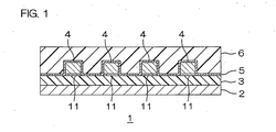
- FIG. 1 is a sectional view of a suspension board with circuit taken as an embodiment of a wired circuit board of the present invention
- the suspension board with circuit 1 shown in FIG. 1 is a suspension board with circuit to be mounted on a hard disc drive.
- the suspension board with circuit 1 comprises a metal supporting board 2, an insulating base layer 3 formed on the metal supporting board 2, a conductive pattern 4 formed on the insulating base layer 3, a metal oxide layer 5 covering the conductive pattern 4, and an insulating cover layer 6 formed over the insulating base layer 3 to cover the conductive pattern 4 by the metal oxide layer 5.
- the metal supporting board 2 is tabular and formed of metal foil or thin planar metal sheet.
- the metals that may be used for forming the metal supporting board 2 include, for example, stainless steel, 42-alloy, aluminum, copper-beryllium, and phosphor bronze, etc.
- stainless steel is used for the metal supporting board 2. It is preferable that the metal supporting board 2 has a thickness of 5-100 ⁇ m.
- the insulating base layer 3 is formed on the metal supporting board 2.
- Insulating materials that may be used for forming the insulating base layer 3 include, for example, synthetic resins commonly used for the insulating material of the wired circuit board, such as, polyimide resin, polyamide imide resin, acrylic resin, polyether nitrile resin, polyether sulfone resin, polyethylene terephthalate resin, polyethylene naphthalate resin and polyvinyl chloride resin, etc. Of these synthetic resins, a polyimide resin is preferably used for the insulating base layer 3.
- the insulating base layer 3 has a thickness of e.g. 5-50 ⁇ m, or preferably 10-30 ⁇ m.
- the conductive pattern 4 formed on the insulating base layer 3 is configured by a plurality of lines of wire spaced apart from each other.
- Conductors that may be used for forming the conductive pattern 4 include, for example, metals commonly used for the conductor of the wired circuit board, such as, copper, nickel, gold, solder, or alloys thereof, etc. Of these metals, copper is preferably used for the conductive pattern 4.
- the conductive pattern 4 has a thickness of e.g. 3-50 ⁇ m, or preferably 5-20 ⁇ m.
- a thin metal film 11 is interposed between the insulating base layer 3 and the conductive pattern 4. Chromium, copper, etc. are preferably used for the thin metal film 11.
- the metal oxide layer 5 is formed to cover a surface (an upper surface and both side surfaces) of the conductive pattern 4.
- the metal oxide layer 5 is formed to extend continuously from the conductive pattern 4 so as to cover the surface of the insulating base layer 3 exposed from the conductive pattern 4 as well.
- the metal oxide layer 5 is formed to be interposed between the conductive pattern 4 and the insulating cover layer 6, as well as between the insulating base layer 3 and the insulating cover layer 6.
- the metal oxide layer 5 is formed from a metal oxide such as, for example, chromium oxide, nickel oxide, copper oxide, titanium oxide, zirconium oxide, indium oxide, aluminum oxide, and zinc oxide, etc.
- chromium oxide is used for the metal oxide layer 5.
- the use of the chromium oxide can form the metal oxide layer 5 to have a steady surface-resistance value with little variation even under a high-temperature and high-humidity environment.
- a degree of oxidation of the metal of the metal oxide layer 5 depends on a formation of the metal oxide layer 5 mentioned layer.
- the metal oxide layer 5 may be uniformly oxidized in the thickness direction or may be nonuniformly oxidized so that the degree of oxidation of its uppermost surface may be the highest and may gradually reduce therefrom inwardly in the thickness direction of metal oxide layer 5.
- the insulating cover layer 6 is formed over the insulating base layer 3 to cover the conductive pattern 4 covered by the metal oxide layer 5.
- the same insulating materials as those for forming the insulating base layer 3 may be used for forming the insulating cover layer 6.
- polyimide resin is used for the insulating cover layer 6.
- the insulating cover layer 6 has a thickness of e.g. 5-50 ⁇ m, or preferably 10-30 ⁇ m.
- This suspension board with circuit 1 can be produced by the method shown in FIGS. 2 and 3, for example.
- the metal supporting board 2 is prepared, as shown in FIG. 2(a).
- the insulating base layer 3 is formed on the metal supporting board 2, as shown in FIG. 2(b).
- the insulating base layer 3 is formed in the manner mentioned below.
- a resin solution containing the synthetic resin cited above is coated on the surface of the metal supporting board 2 and then dried, then cured by heating.
- the resin solution is coated by a known method, such as, for example, a doctor blade method and a spin coat method.
- a known photosensitizing agent may be mixed in the resin solution.
- the insulating base layer 3 can be in the form of a pattern by coating the resin solution is coated on the metal supporting board 2, and by exposing to light and developing thereafter.
- the insulating base layer 3 may be formed by a method that after a previously processed dry film of synthetic resin is adhesively bonded to the metal supporting board 2 via an adhesive layer as needed.
- the conductive pattern 4 is formed on the insulating base layer 3.
- the conductive pattern 4 is formed on the surface of the insulating base layer 3 by a known patterning process such as a subtractive process or an additive process, without any particular limitation on the process.
- a conductor layer is first laminated on the entire surface of the insulating base layer 3 via an adhesive layer as needed. Then, an etching resist corresponding to the conductive pattern 4 is formed on the conductor layer. Then, with this etching resist as the resist, the conductor layer is etched and, thereafter, the etching resist is removed.
- a thin metal film serving as a seed film (a ground layer) is formed on the surface of the insulating base layer 3, first. Then, a plating resist is formed on the surface of the thin metal film to have a pattern reverse to the conductive pattern 4. Then, the conductive pattern 4 is formed on a surface of the thin metal film exposed from the plating resist by plating. Thereafter, the plating resist is removed and all areas of the thin metal film except its parts corresponding to the conductive pattern 4 are removed.
- the additive process is preferably used to form a finer pattern for the conductive pattern 4.
- the thin metal film 11 serving as the seed film (ground layer) is formed on the entire surface of insulating base layer 3, first, as shown in FIG. 2(c).
- the thin metal film 11 is formed by a vacuum vapour-deposition process, particularly a sputtering vapour-deposition process.
- a thin chrome film and a thin copper film are preferably formed in sequence on the entire surface of the insulating base layer 3 by the sputtering vapour-deposition process.
- the thin chrome film is set to have a thickness of 100-600 ⁇ and the thin copper film has a thickness of 500-2,000 ⁇ .
- a plating resist 12 is formed on the thin metal film 11, as shown in FIG. 2(d).
- the plating resist 12 is formed in the form of the resist pattern reverse to the conductive pattern 4 by a known process for exposing to light and developing using a dry film photoresist, for example.
- the conductor layer 4 is formed on the thin metal film 11 exposed from the plating resist 12, as shown in FIG. 2(e). Electrolytic plating may be used to form the conductor layer 4, preferably electrolytic copper plating is used therefor.
- the plating resist 12 is removed by a known etching process, such as a chemical etching (wet etching), or by stripping, as shown in FIG. 3(f).
- a known etching process such as a chemical etching (wet etching), or by stripping, as shown in FIG. 3(f).
- a portion of the thin metal film 11 exposed from the conductive pattern 4 is removed by the known etching process, such as the chemical etching (wet etching), as shown in FIG. 3(g).
- the metal oxide layer 5 is formed on the surface of the conductive pattern 4 and on the surface of the insulating base layer 3 by the sputtering process, as shown in FIG. 3(h).
- the metal oxide layer 5 can be formed, for example, by a process of sputtering using a metal as a target, and oxidizing by heating as needed, by a process of reactive sputtering, or a process of sputtering using a metal oxide as the target.
- a sputtering apparatus shown in FIG. 4 is used for the sputtering.
- a target 22 and an earth electrode 23 are arranged opposite to each other at a predetermined space in a vacuum chamber 21, as shown in FIG. 4.
- a power source 24 is connected to the target 22, and a plasma emission monitor 25 is arranged to emit plasma to the target 22.
- a pulsed power source, a direct current (DC) power source, an alternate current (RF) power source, etc. may be used as the power source 24,
- the earth electrode 23 is electrically grounded, and a board 26 is placed on a surface of the earth electrode 23.
- the board 26 is the suspension board with circuit 1 prepared in the process shown in FIG. 3(g) and the board 26 on the side thereof on which the conductive pattern 4 is provided is arranged opposite to the target 22.
- the metals that may be used for the target 22 include, for example, chromium, nickel, copper, titanium, aluminum, tantalum, lead, zinc, zirconium, gallium, indium, and alloys thereof, etc.
- chromium is used for the target 22.
- an inert gas such as argon gas
- an electric power is applied from the power source 24, so that the target 22 is sputtered for a predetermined time while plasma emission intensity is maintained at a constant value by the plasma emission monitor 25.
- a sputtering coating is formed on the surface of the conductive pattern 4 and on the surface of the insulating base layer 3 to continuously extend thereon.
- Sputtering time 1 second to 15 minutes
- Sputtering time 1 second to 15 minutes.
- an adequate sputtering is selected from known sputtering methods, such as direct current sputtering, ration frequency sputtering, magnetron sputtering, or combination thereof.
- the sputtering coating is oxidized by heating as needed.
- the sputtering coating is heated in a heating furnace in the atmosphere.
- the heating temperature is in a range of e.g. 280°C-310°C, or preferably about 300°C.
- the heating temperature is in a range of e.g. 110°C-140°C, or preferably about 125°C.
- the heating time in both conditions 1 and 2 is preferably in a range of e.g. one minute to twelve hours.
- the metal oxide layer 5 is formed to continuously extend along the surface of the conductive pattern 4 and the surface of the insulating base layer 3, as shown in FIG. 3(h).
- the sputtering coating is naturally oxidized under air exposure, then the sputtering coating need not particularly be heated or may be heated to form a steady metal oxide layer.
- This metal oxide layer 5 is nonuniformly oxidized so that the degree of oxidation of its uppermost surface is the highest and gradually reduces therefrom inwardly in the thickness direction of metal oxide layer 5.
- the metal oxide layer 5 thus formed has a thickness of e.g. 5-100nm under the sputtering condition 1 as well as under the sputtering condition 2.
- the same metal as the metal used for forming the sputtering coating mentioned above is used as the target 22 and set in place. Also, the thin metal film 11 of the suspension board with circuit 1 which is in the process of production as shown in FIG. 3(g) is placed so that the board 26 on the side thereof on which the conductive pattern 4 is arranged opposite to the target 22.
- a reactive gas including argon or nitrogen, and oxygen of an essential gas are mixed in a given proportion (e.g. Ar/O 2 mixed gas) is introduced in the vacuum chamber 21, so that the target 22 is sputtered for a predetermined time while the plasma emission intensity is maintained at a constant value by the plasma emission monitor 25.
- a reactive gas including argon or nitrogen, and oxygen of an essential gas are mixed in a given proportion (e.g. Ar/O 2 mixed gas) is introduced in the vacuum chamber 21, an electric power is applied to the target 22 from the power source 24, so that the target 22 is sputtered for a predetermined time while the plasma emission intensity is maintained at a constant value by the plasma emission monitor 25.
- the metal oxide layer 5 is formed on the surface of the conductive pattern 4 and on the surface of the insulating base layer 3 to continuously extend thereon, as shown in FIG. 3(h).
- the metal oxide layer 5 thus formed is uniformly oxidized in the thickness direction.
- Sputtering time 1 second to 15 minutes
- the metal oxide layer 5 thus formed has a thickness of e.g. 5-200nm.
- the same processes as those described above can be taken, except that the metal oxide is used as the target 22 and also the alternate current power source is used as the power source 24 in the sputtering apparatus shown in FIG. 4.
- the metal oxides that may be used as the target 22 include, for example, chromium oxide, zirconium oxide, silicon oxide, tin oxide, titanium oxide, magnesium oxide, and aluminum oxide.
- chromium oxide is used as the target.
- the metal oxide cited above is used as the target 22, and the suspension board with circuit 1 which is in the process of production as shown in FIG. 3(g) is placed so that the board 26 on the side thereof on which the conductive pattern 4 is arranged opposite to the target 22.
- the metal oxide layer 5 is formed on the surface of the conductive pattern 4 and on the surface of the insulating base layer 3 to continuously extend thereon, as shown in FIG. 3(h).
- the metal oxide layer 5 thus formed is uniformly oxidized in the thickness direction.
- Sputtering time 1 second to 15 minutes
- the metal oxide layer 5 thus formed has a thickness of e.g. 5-300nm.
- the metal oxide layer 5 has a surface resistance preferably in a range of not less than 10 12 ⁇ / ⁇ , or further preferably in a range of between 1 ⁇ 10 13 ⁇ / ⁇ and usually not more than 1 ⁇ 10 15 ⁇ / ⁇ .
- the insulating cover layer 6 is formed over the insulating base layer 3 to cover the conductive pattern 4 covered by the metal oxide layer 5, as shown in FIG. 3(i).
- the suspension board with circuit 1 is obtained in the manner described above.
- a resin solution containing the synthetic resin cited above is coated over the insulating base layer 3 (specifically on the metal oxide layer 5 formed on the surface of the insulting base layer 3) to cover the conductive pattern 4 covered by the metal oxide layer 5 in the same manner as in the above and then is cured by heating, thereby to produce the insulating cover layer 6.
- a known photosensitizing agent may be mixed in the resin solution.
- the insulating cover layer 6 can be in the form of a pattern by a method that the resin solution is coated over the insulating base layer 3 to cover the conductive pattern 4 covered by the metal oxide layer 5, and exposed to light and then developed thereafter.
- the metal oxide layer 5 since the metal oxide layer 5 is formed by the sputtering process, the metal oxide layer 5 can be formed with a uniform thickness. Hence, the metal oxide layer 5 can fully function as a barrier layer to the conductive pattern 4 to prevent the metal for forming the conductive pattern 4 from diffusing in the insulating cover layer 6. As a result of this, deterioration of the conductive pattern 4 and short-circuiting of the conductive copper layer 4 can be prevented effectively.
- the wired circuit board of the present invention includes a single-sided flexible wired circuit board, a double-sided flexible wired circuit board, and a multilayer flexible wired circuit board.
- a single-sided flexible wired circuit board 31 comprises the insulating base layer 3, the conductive pattern 4 formed on the insulating base layer 3, the metal oxide layer 5 formed on the surface of the conductive pattern 4 and on the surface of the insulating base layer 3 by sputtering, and the insulating cover layer 6 formed over the insulating base layer 3 to cover the conductive pattern 4 covered by the metal oxide layer 5, as shown in FIG, 5.
- the metal oxide layer 5 may be formed on the surface of the conductive pattern 4 only.
- a metal supporting board of a stainless foil of 25 ⁇ m thick was prepared (cf. FIG. 2(a)). Then, a resin solution of a precursor of a photosensitive polyimide resin was coated over the metal supporting board. After dried, the coated resin solution was cured by heating. Thereafter, it was exposed to light and then developed. The insulating base layer of a polyimide resin of 10 ⁇ m thick was formed on the metal supporting board in the manner mentioned above (cf. FIG. 2(b)).
- a thin chromium film and a thin copper film were formed in sequence on the entire surface of the insulating base layer to form a thin metal film of 2,000 ⁇ thick by a sputtering vapour-deposition method (cf. FIG. 2(c)).
- a resist pattern reverse to the conductive pattern was formed on the thin metal film by exposing to light and developing using a dry film resist (cf. FIG. 2(d)).
- the plating resist was removed by chemical etching (cf. FIG. 3(f)) and, then, the thin metal film exposed from the conductive pattern was also removed by the chemical etching (cf. FIG. 3(g)).
- the thin metal film formed by the sputtering was oxidized by a heating to thereby to form a metal oxide layer on the surface of the conductive pattern and on the surface of the insulating cover layer.
- the sputtering was carried out in the same manner as in the sputtering mentioned above and under the conditions mentioned below:
- the surface of the thin metal film formed by a thin chromium film was oxidized by heating at 300°C for 12 hours in the atmosphere, whereby the metal oxide layer was formed on the thin metal film (cf. FIG. 3(h)).
- the thickness of the metal oxide layer was 8nm.
- the presence of the metal oxide layer was confirmed by ESCA. Also, when a surface resistance of the metal oxide layer was measured at a temperature of 25°C and a humidity of 15%, using a surface resistance measuring device (Hiresta-up MCP-HT450 available from Mitsubishi Chemical Corporation, it was 2.1 ⁇ 10 12 ⁇ / ⁇ .
- Example 2 The same operations as in Example 1 were conducted to produce the suspension board with circuit except that the conditions in the formation of the metal oxide layer of Example 1, for the sputtering and the oxidization-by-heating after sputtering were modified as follows:
- Heating temperature after sputtering 125°C
- the thickness of the metal oxide layer obtained was 6nm.
- Example 2 The same operations as in Example 1 were conducted to produce the suspension board with circuit except that in the formation of the metal oxide layer of Example 1, the sputtering was carried out under the following conditions and the sputtering coating formed was not oxidized after heating.
- the thickness of the metal oxide layer obtained was 20nm.
- Example 2 The same operations as in Example 1 were conducted to produce the suspension board with circuit except that in the formation of the metal oxide layer of Example 1, the sputtering was carried out under the following conditions and the sputtering coating formed was not oxidized after heating.
- the thickness of the metal oxide layer obtained was 300nm.
Landscapes
- Engineering & Computer Science (AREA)
- Manufacturing & Machinery (AREA)
- Microelectronics & Electronic Packaging (AREA)
- Manufacturing Of Printed Wiring (AREA)
- Insulated Metal Substrates For Printed Circuits (AREA)
- Non-Metallic Protective Coatings For Printed Circuits (AREA)
- Laminated Bodies (AREA)
- Parts Printed On Printed Circuit Boards (AREA)
Abstract
Description
- This application claims priority from
Japanese Patent Application No. 2005-257071, filed on September 5, 2005 - The present invention relates to a wired circuit board and, more particularly, to a wired circuit board such as a flexible wired circuit board and a suspension board with circuit.
- A wired circuit board, such as a flexible wired circuit board and a suspension board with circuit, comprises in general an insulating base layer of e.g. polyimide resin, a conductive layer of copper foil e.g. formed on the insulating base layer, and an insulating cover layer of e.g. polyimide resin formed on the insulating base layer for covering the conductive layer. This wired circuit board is widely used in various fields of electric and electronic devices and equipment.
- Meanwhile, there has been proposed an improvement of this wired circuit board, according to which a thin nickel film is formed on a surface of a conductive copper layer by electroless nickel plating to cover the surface of the conductive copper layer (cf.
JP Laid-open (Unexamined) Patent Publication No. Hei 10-12983 - The proposed thin nickel film described in
JP Laid-open (Unexamined) Patent Publication No. Hei 10-12983 - However, since this proposed thin nickel film described in
JP Laid-open (Unexamined) Patent Publication No. Hei 10-12983 - It is an object of the invention to provide a wired circuit board that can prevent deterioration of a conductive pattern and short-circuiting of the conductive pattern.
- To achieve the object described above, the present invention provides a wired circuit board comprising an insulating base layer, a conductive pattern formed on the insulating base layer, a metal oxide layer formed to cover the conductive pattern by sputtering, and an insulating cover layer formed over the insulating base layer to cover the conductive pattern covered by the metal oxide layer.
- It is preferable that in the wired circuit board of the present invention, a surface resistance of the metal oxide layer is not less than 1012Ω/□.
- According to the wired circuit board of the present invention, since the metal oxide layer is formed by the sputtering, the metal oxide layer can be formed in a uniform thickness. Hence, the metal oxide layer can fully function as a barrier layer to the conductive pattern and, accordingly, deterioration of the conductive pattern and short-circuiting of the conductive pattern can be prevented effectively.
- In the drawings:
- FIG. 1 is a sectional view of a suspension board with circuit taken as an embodiment of a wired circuit board of the present invention,
- FIG. 2 is a process drawing of the suspension board with circuit shown in FIG. 1,
- (a) showing the step of preparing a metal supporting board,
- (b) showing the step of forming an insulating base layer on the metal supporting board,
- (c) showing the step of forming a thin metal film on the entire area of a surface of the insulating base layer,
- (d) showing the step of forming a plating resist on the thin meal film, and
- (e) showing the step of forming a conductive pattern on the thin metal film exposed from the plating resist,
- FIG. 3 is the process drawing of the suspension board with circuit which is subsequent to FIG. 2;
- (f) showing the step of removing the plating resist,
- (g) showing the step of removing the thin metal film exposed from the conductive pattern,
- (h) showing the step of forming a metal oxide layer by sputtering, and
- (i) showing the step of forming an insulating cover layer on a surface of the conductive pattern and on the metal oxide layer formed on the surface of the insulating base layer,
- FIG. 4 is a schematic view showing the structure of a sputtering apparatus in an embodiment, and
- FIG. 5 is a sectional view of a single-sided flexible wired circuit board taken as another embodiment of the wired circuit board of the present invention.
- FIG. 1 is a sectional view of a suspension board with circuit taken as an embodiment of a wired circuit board of the present invention,
- The suspension board with
circuit 1 shown in FIG. 1 is a suspension board with circuit to be mounted on a hard disc drive. The suspension board withcircuit 1 comprises ametal supporting board 2, aninsulating base layer 3 formed on themetal supporting board 2, aconductive pattern 4 formed on theinsulating base layer 3, ametal oxide layer 5 covering theconductive pattern 4, and aninsulating cover layer 6 formed over theinsulating base layer 3 to cover theconductive pattern 4 by themetal oxide layer 5. - The
metal supporting board 2 is tabular and formed of metal foil or thin planar metal sheet. The metals that may be used for forming themetal supporting board 2 include, for example, stainless steel, 42-alloy, aluminum, copper-beryllium, and phosphor bronze, etc. Preferably, stainless steel is used for themetal supporting board 2. It is preferable that themetal supporting board 2 has a thickness of 5-100µm. - The
insulating base layer 3 is formed on themetal supporting board 2. Insulating materials that may be used for forming theinsulating base layer 3 include, for example, synthetic resins commonly used for the insulating material of the wired circuit board, such as, polyimide resin, polyamide imide resin, acrylic resin, polyether nitrile resin, polyether sulfone resin, polyethylene terephthalate resin, polyethylene naphthalate resin and polyvinyl chloride resin, etc. Of these synthetic resins, a polyimide resin is preferably used for theinsulating base layer 3. Theinsulating base layer 3 has a thickness of e.g. 5-50µm, or preferably 10-30µm. - The
conductive pattern 4 formed on theinsulating base layer 3 is configured by a plurality of lines of wire spaced apart from each other. Conductors that may be used for forming theconductive pattern 4 include, for example, metals commonly used for the conductor of the wired circuit board, such as, copper, nickel, gold, solder, or alloys thereof, etc. Of these metals, copper is preferably used for theconductive pattern 4. Theconductive pattern 4 has a thickness of e.g. 3-50µm, or preferably 5-20µm. - When the
conductive pattern 4 is formed by an additive process, athin metal film 11 is interposed between theinsulating base layer 3 and theconductive pattern 4. Chromium, copper, etc. are preferably used for thethin metal film 11. - The
metal oxide layer 5 is formed to cover a surface (an upper surface and both side surfaces) of theconductive pattern 4. Themetal oxide layer 5 is formed to extend continuously from theconductive pattern 4 so as to cover the surface of theinsulating base layer 3 exposed from theconductive pattern 4 as well. In other words, themetal oxide layer 5 is formed to be interposed between theconductive pattern 4 and theinsulating cover layer 6, as well as between theinsulating base layer 3 and theinsulating cover layer 6. - The
metal oxide layer 5 is formed from a metal oxide such as, for example, chromium oxide, nickel oxide, copper oxide, titanium oxide, zirconium oxide, indium oxide, aluminum oxide, and zinc oxide, etc. Preferably chromium oxide is used for themetal oxide layer 5. The use of the chromium oxide can form themetal oxide layer 5 to have a steady surface-resistance value with little variation even under a high-temperature and high-humidity environment. - A degree of oxidation of the metal of the
metal oxide layer 5 depends on a formation of themetal oxide layer 5 mentioned layer. Themetal oxide layer 5 may be uniformly oxidized in the thickness direction or may be nonuniformly oxidized so that the degree of oxidation of its uppermost surface may be the highest and may gradually reduce therefrom inwardly in the thickness direction ofmetal oxide layer 5. - The
insulating cover layer 6 is formed over theinsulating base layer 3 to cover theconductive pattern 4 covered by themetal oxide layer 5. The same insulating materials as those for forming the insulatingbase layer 3 may be used for forming the insulatingcover layer 6. Preferably, polyimide resin is used for the insulatingcover layer 6. The insulatingcover layer 6 has a thickness of e.g. 5-50µm, or preferably 10-30µm. - This suspension board with
circuit 1 can be produced by the method shown in FIGS. 2 and 3, for example. - First, the
metal supporting board 2 is prepared, as shown in FIG. 2(a). - Then, the insulating
base layer 3 is formed on themetal supporting board 2, as shown in FIG. 2(b). - For example, the insulating
base layer 3 is formed in the manner mentioned below. A resin solution containing the synthetic resin cited above is coated on the surface of themetal supporting board 2 and then dried, then cured by heating. - The resin solution is coated by a known method, such as, for example, a doctor blade method and a spin coat method.
- A known photosensitizing agent may be mixed in the resin solution. When using this resin solution, the insulating
base layer 3 can be in the form of a pattern by coating the resin solution is coated on themetal supporting board 2, and by exposing to light and developing thereafter. - Alternatively, the insulating
base layer 3 may be formed by a method that after a previously processed dry film of synthetic resin is adhesively bonded to themetal supporting board 2 via an adhesive layer as needed. - Then, the
conductive pattern 4 is formed on the insulatingbase layer 3. - The
conductive pattern 4 is formed on the surface of the insulatingbase layer 3 by a known patterning process such as a subtractive process or an additive process, without any particular limitation on the process. - When the
conductive pattern 4 is formed by the subtractive process, a conductor layer is first laminated on the entire surface of the insulatingbase layer 3 via an adhesive layer as needed. Then, an etching resist corresponding to theconductive pattern 4 is formed on the conductor layer. Then, with this etching resist as the resist, the conductor layer is etched and, thereafter, the etching resist is removed. - When the
conductive pattern 4 is formed by the additive process, a thin metal film serving as a seed film (a ground layer) is formed on the surface of the insulatingbase layer 3, first. Then, a plating resist is formed on the surface of the thin metal film to have a pattern reverse to theconductive pattern 4. Then, theconductive pattern 4 is formed on a surface of the thin metal film exposed from the plating resist by plating. Thereafter, the plating resist is removed and all areas of the thin metal film except its parts corresponding to theconductive pattern 4 are removed. - Of these patterning processes, in order to realize high-density wiring, the additive process is preferably used to form a finer pattern for the
conductive pattern 4. - In the additive process, the
thin metal film 11 serving as the seed film (ground layer) is formed on the entire surface of insulatingbase layer 3, first, as shown in FIG. 2(c). Thethin metal film 11 is formed by a vacuum vapour-deposition process, particularly a sputtering vapour-deposition process. - To be more specific, for example a thin chrome film and a thin copper film are preferably formed in sequence on the entire surface of the insulating
base layer 3 by the sputtering vapour-deposition process. In the formation of thethin metal film 11, the thin chrome film is set to have a thickness of 100-600 Å and the thin copper film has a thickness of 500-2,000 Å. - Subsequently, a plating resist 12 is formed on the
thin metal film 11, as shown in FIG. 2(d). The plating resist 12 is formed in the form of the resist pattern reverse to theconductive pattern 4 by a known process for exposing to light and developing using a dry film photoresist, for example. - Then, the
conductor layer 4 is formed on thethin metal film 11 exposed from the plating resist 12, as shown in FIG. 2(e). Electrolytic plating may be used to form theconductor layer 4, preferably electrolytic copper plating is used therefor. - Then, the plating resist 12 is removed by a known etching process, such as a chemical etching (wet etching), or by stripping, as shown in FIG. 3(f).
- Then, a portion of the
thin metal film 11 exposed from the conductive pattern 4 (or an area of thethin metal film 11 where the plating resist 12 is formed) is removed by the known etching process, such as the chemical etching (wet etching), as shown in FIG. 3(g). - Then, the
metal oxide layer 5 is formed on the surface of theconductive pattern 4 and on the surface of the insulatingbase layer 3 by the sputtering process, as shown in FIG. 3(h). - No particular limitation is imposed on the process of forming the
metal oxide layer 5 by the sputtering. Themetal oxide layer 5 can be formed, for example, by a process of sputtering using a metal as a target, and oxidizing by heating as needed, by a process of reactive sputtering, or a process of sputtering using a metal oxide as the target. - In the process whereof the sputtering using the metal as the target to form a thin metal layer and, then, oxidizing by heating, as needed, the surface of the
conductive pattern 4 and the surface of the insulatingbase layer 3 exposed from theconductive pattern 4 are first subjected to the sputtering using the metal as the target. - For example, a sputtering apparatus shown in FIG. 4 is used for the sputtering. Specifically, in the sputtering apparatus, a
target 22 and anearth electrode 23 are arranged opposite to each other at a predetermined space in avacuum chamber 21, as shown in FIG. 4. Apower source 24 is connected to thetarget 22, and a plasma emission monitor 25 is arranged to emit plasma to thetarget 22. A pulsed power source, a direct current (DC) power source, an alternate current (RF) power source, etc. may be used as thepower source 24, - The
earth electrode 23 is electrically grounded, and aboard 26 is placed on a surface of theearth electrode 23. (Theboard 26 is the suspension board withcircuit 1 prepared in the process shown in FIG. 3(g) and theboard 26 on the side thereof on which theconductive pattern 4 is provided is arranged opposite to thetarget 22.) - The metals that may be used for the
target 22 include, for example, chromium, nickel, copper, titanium, aluminum, tantalum, lead, zinc, zirconium, gallium, indium, and alloys thereof, etc. Preferably, chromium is used for thetarget 22. - Then, after an inert gas, such as argon gas, is introduced into the
vacuum chamber 21, an electric power is applied from thepower source 24, so that thetarget 22 is sputtered for a predetermined time while plasma emission intensity is maintained at a constant value by the plasma emission monitor 25. As a result of this, a sputtering coating is formed on the surface of theconductive pattern 4 and on the surface of the insulatingbase layer 3 to continuously extend thereon. - An example of the sputtering conditions for the sputtering using this metal as the target is given below:
- Ultimate vacuum: 1.33 × 10⁻⁵ Pa to 1.33 × 10⁻² Pa
- Flow rate of introduced gas (Argon): 1.2 × 10⁻³ m3/h to 4 × 10⁻³ m3/h
- Operating pressure (Degree of vacuum after introduction of introduced gas): 1.33 × 10⁻²Pa to 1.33 Pa
- Temperature of earth electrode: 10°C-100°C
- Electric power: 100W-2,000W
- Sputtering time: 1 second to 15 minutes
- Ultimate vacuum: 1.33 × 10⁻⁵ Pa to 1.33 × 10⁻² Pa
- Flow rate of introduced gas (Argon): 1.2 × 10⁻³ m3/h to 4 × 10⁻³ m3/h
- Operating pressure (Degree of vacuum after introduction of introduced gas): 1.33 × 10⁻² Pa to 1.33 Pa
- Temperature of earth electrode: 10°C-100°C
- Electric power: 10W-130W
- Sputtering time: 1 second to 15 minutes.
- In this sputtering, an adequate sputtering is selected from known sputtering methods, such as direct current sputtering, ration frequency sputtering, magnetron sputtering, or combination thereof.
- Then, the sputtering coating is oxidized by heating as needed. No particular limitation is imposed on the way of heating. For example, the sputtering coating is heated in a heating furnace in the atmosphere. In the
sputtering condition 1, the heating temperature is in a range of e.g. 280°C-310°C, or preferably about 300°C. In thesputtering condition 2, the heating temperature is in a range of e.g. 110°C-140°C, or preferably about 125°C. The heating time in bothconditions metal oxide layer 5 is formed to continuously extend along the surface of theconductive pattern 4 and the surface of the insulatingbase layer 3, as shown in FIG. 3(h). - If the sputtering coating is naturally oxidized under air exposure, then the sputtering coating need not particularly be heated or may be heated to form a steady metal oxide layer.
- This
metal oxide layer 5 is nonuniformly oxidized so that the degree of oxidation of its uppermost surface is the highest and gradually reduces therefrom inwardly in the thickness direction ofmetal oxide layer 5. - The
metal oxide layer 5 thus formed has a thickness of e.g. 5-100nm under thesputtering condition 1 as well as under thesputtering condition 2. - In the reactive sputtering, the same processes as those described above are taken, except the process of introducing the introduced gas comprising oxygen in the
vacuum chamber 21, using the sputtering apparatus shown in FIG. 4. - To be more specific, the same metal as the metal used for forming the sputtering coating mentioned above is used as the
target 22 and set in place. Also, thethin metal film 11 of the suspension board withcircuit 1 which is in the process of production as shown in FIG. 3(g) is placed so that theboard 26 on the side thereof on which theconductive pattern 4 is arranged opposite to thetarget 22. - Then, after a reactive gas including argon or nitrogen, and oxygen of an essential gas are mixed in a given proportion (e.g. Ar/O2 mixed gas) is introduced in the
vacuum chamber 21, an electric power is applied to thetarget 22 from thepower source 24, so that thetarget 22 is sputtered for a predetermined time while the plasma emission intensity is maintained at a constant value by the plasma emission monitor 25. - As a result of this, the
metal oxide layer 5 is formed on the surface of theconductive pattern 4 and on the surface of the insulatingbase layer 3 to continuously extend thereon, as shown in FIG. 3(h). Themetal oxide layer 5 thus formed is uniformly oxidized in the thickness direction. - An example of the sputtering conditions for this reactive sputtering is given below:
- Ultimate vacuum: 1.33 × 10⁻⁵ Pa to 1.33 × 10⁻² Pa
- Flow rate of introduced gas (Argon): Ar: 1.2 × 10⁻³ m3/h to 4 × 10⁻³ m3/h
- Flow rate of introduced gas (Oxigen): O2: 6 × 10⁻⁵ m3/h to 30 × 10-5 m3/h
- Operating pressure (Degree of vacuum after introduction of introduced gas): 1.33 × 10⁻² Pa to 1.33 Pa
- Temperature of earth electrode: 10°C-100°C
- Electric power: 10W-2,000W
- Sputtering time: 1 second to 15 minutes
- The
metal oxide layer 5 thus formed has a thickness of e.g. 5-200nm. - In the sputtering using a metal oxide as the target, the same processes as those described above can be taken, except that the metal oxide is used as the
target 22 and also the alternate current power source is used as thepower source 24 in the sputtering apparatus shown in FIG. 4. The metal oxides that may be used as thetarget 22 include, for example, chromium oxide, zirconium oxide, silicon oxide, tin oxide, titanium oxide, magnesium oxide, and aluminum oxide. Preferably, chromium oxide is used as the target. - To be more specific, the metal oxide cited above is used as the
target 22, and the suspension board withcircuit 1 which is in the process of production as shown in FIG. 3(g) is placed so that theboard 26 on the side thereof on which theconductive pattern 4 is arranged opposite to thetarget 22. - Then, after an inert gas of argon is introduced as the introduced gas in the
vacuum chamber 21, an electric power is applied from thepower source 24, so that thetarget 22 is sputtered for a predetermined time while plasma emission intensity is maintained at a constant value by the plasma emission monitor 25. As a result of this, themetal oxide layer 5 is formed on the surface of theconductive pattern 4 and on the surface of the insulatingbase layer 3 to continuously extend thereon, as shown in FIG. 3(h). Themetal oxide layer 5 thus formed is uniformly oxidized in the thickness direction. - An example of the sputtering conditions for this sputtering using this metal oxide as the target is given below.
- Ultimate vacuum: 1.33 × 10⁻⁵ Pa to 1.33 × 10⁻² Pa
- Flow rate of introduced gas (Argon): 1.2 × 10⁻³ m3/h to 4 × 10⁻³ m3/h
- Operating pressure (Degree of vacuum after introduction of introduced gas): 1.33 × 10⁻² Pa to 1.33 Pa
- Temperature of earth electrode: 10°C-100°C
- Electric power: 10W-2,000W
- Sputtering time: 1 second to 15 minutes
- The
metal oxide layer 5 thus formed has a thickness of e.g. 5-300nm. - Also, the
metal oxide layer 5 has a surface resistance preferably in a range of not less than 1012Ω/□, or further preferably in a range of between 1 × 10¹³Ω/□ and usually not more than 1 × 10¹⁵Ω/□. - Then, the insulating
cover layer 6 is formed over the insulatingbase layer 3 to cover theconductive pattern 4 covered by themetal oxide layer 5, as shown in FIG. 3(i). The suspension board withcircuit 1 is obtained in the manner described above. - A resin solution containing the synthetic resin cited above is coated over the insulating base layer 3 (specifically on the
metal oxide layer 5 formed on the surface of the insulting base layer 3) to cover theconductive pattern 4 covered by themetal oxide layer 5 in the same manner as in the above and then is cured by heating, thereby to produce the insulatingcover layer 6. A known photosensitizing agent may be mixed in the resin solution. When using this resin solution, the insulatingcover layer 6 can be in the form of a pattern by a method that the resin solution is coated over the insulatingbase layer 3 to cover theconductive pattern 4 covered by themetal oxide layer 5, and exposed to light and then developed thereafter. - According to this suspension board with
circuit 1, since themetal oxide layer 5 is formed by the sputtering process, themetal oxide layer 5 can be formed with a uniform thickness. Hence, themetal oxide layer 5 can fully function as a barrier layer to theconductive pattern 4 to prevent the metal for forming theconductive pattern 4 from diffusing in the insulatingcover layer 6. As a result of this, deterioration of theconductive pattern 4 and short-circuiting of theconductive copper layer 4 can be prevented effectively. - Although the suspension board with
circuit 1 has been illustrated above as an example of the wired circuit board of the present invention, the wired circuit board of the present invention includes a single-sided flexible wired circuit board, a double-sided flexible wired circuit board, and a multilayer flexible wired circuit board. - For example, a single-sided flexible
wired circuit board 31 comprises the insulatingbase layer 3, theconductive pattern 4 formed on the insulatingbase layer 3, themetal oxide layer 5 formed on the surface of theconductive pattern 4 and on the surface of the insulatingbase layer 3 by sputtering, and the insulatingcover layer 6 formed over the insulatingbase layer 3 to cover theconductive pattern 4 covered by themetal oxide layer 5, as shown in FIG, 5. - Although the embodiment in which the
metal oxide layer 5 is formed on the surface of theconductive pattern 4 and on the surface of the insulatingbase layer 3 has been described above, themetal oxide layer 5 may be formed on the surface of theconductive pattern 4 only. - Examples
- While in the following, the present invention will be described in further detail with reference to Examples, the present invention is not limited to any of the examples.
- Example 1
- A metal supporting board of a stainless foil of 25 µm thick was prepared (cf. FIG. 2(a)). Then, a resin solution of a precursor of a photosensitive polyimide resin was coated over the metal supporting board. After dried, the coated resin solution was cured by heating. Thereafter, it was exposed to light and then developed. The insulating base layer of a polyimide resin of 10 µm thick was formed on the metal supporting board in the manner mentioned above (cf. FIG. 2(b)).
- Then, a thin chromium film and a thin copper film were formed in sequence on the entire surface of the insulating base layer to form a thin metal film of 2,000Å thick by a sputtering vapour-deposition method (cf. FIG. 2(c)).
- Then, a resist pattern reverse to the conductive pattern was formed on the thin metal film by exposing to light and developing using a dry film resist (cf. FIG. 2(d)).
- Then, a conductive pattern of 10 µm thick was formed on the
thin metal film 11 exposed from the plating resist by electrolytic copper plating (cf. FIG. 2(e)). - Then, the plating resist was removed by chemical etching (cf. FIG. 3(f)) and, then, the thin metal film exposed from the conductive pattern was also removed by the chemical etching (cf. FIG. 3(g)).
- Then, after the sputtering was carried out using a metal as a target, the thin metal film formed by the sputtering was oxidized by a heating to thereby to form a metal oxide layer on the surface of the conductive pattern and on the surface of the insulating cover layer.
- The sputtering was carried out in the same manner as in the sputtering mentioned above and under the conditions mentioned below:
- Target: Chromium
- Ultimate vacuum: 1.33 × 10⁻⁴ Pa
- Flow rate of introduced gas (Argon): 2 × 10⁻³ m3/h
- Operating pressure: 0.13 Pa
- Temperature of earth electrode: 60°C
- Electric power: DC150W
- Sputtering time: 5 seconds
- Subsequently, the surface of the thin metal film formed by a thin chromium film was oxidized by heating at 300°C for 12 hours in the atmosphere, whereby the metal oxide layer was formed on the thin metal film (cf. FIG. 3(h)). The thickness of the metal oxide layer was 8nm.
- The presence of the metal oxide layer was confirmed by ESCA. Also, when a surface resistance of the metal oxide layer was measured at a temperature of 25°C and a humidity of 15%, using a surface resistance measuring device (Hiresta-up MCP-HT450 available from Mitsubishi Chemical Corporation, it was 2.1 × 10¹²Ω/□.
- Then, a resin solution of a precursor of a photosensitive polyimide resin was coated over the surface of the insulating base layer and the surface of the conductive pattern. After dried, it was cured by heating. Thereafter, it was exposed to light and then developed, to form the insulating base layer of a polyimide resin of 5 µm thick. The suspension board with circuit was produced by the method described above (cf. FIG. 3(i)).
- Example 2
- The same operations as in Example 1 were conducted to produce the suspension board with circuit except that the conditions in the formation of the metal oxide layer of Example 1, for the sputtering and the oxidization-by-heating after sputtering were modified as follows:
- Target: Chromium
- Ultimate vacuum: 1.33 × 10⁻⁴ Pa
- Flow rate of introduced gas (Argon): 2 × 10⁻³ m3/h
- Operating pressure: 0.13 Pa
- Temperature of earth electrode: 60°C
- Electric power: DC120W
- Sputtering time: 5 seconds
- Heating temperature after sputtering: 125°C
- Heating time after sputtering: 12 hours
- The thickness of the metal oxide layer obtained was 6nm.
- When a surface resistance of the metal oxide layer formed was measured at a temperature of 25°C and a humidity of 15%, using the surface resistance measuring device (Hiresta-up MCP-HT450 available from Mitsubishi Chemical Corporation, it was 8.8 × 10¹²Ω/□.
- Example 3
- The same operations as in Example 1 were conducted to produce the suspension board with circuit except that in the formation of the metal oxide layer of Example 1, the sputtering was carried out under the following conditions and the sputtering coating formed was not oxidized after heating.
- Target: Chromium
- Ultimate vacuum: 1.33 × 10⁻⁴ Pa
- Flow rate of introduced gas (Argon): 2 × 10⁻³ m3/h
- Flow rate of introduced gas (Oxygen): 1 × 10⁻⁴ m3/h
- Operating pressure: 0.13 Pa
- Temperature of earth electrode: 60°C
- Electric power: DC300W
- Sputtering time: 15 seconds
- The thickness of the metal oxide layer obtained was 20nm.
- When a surface resistance of the metal oxide layer formed was measured at a temperature of 25°C and a humidity of 15%, using the surface resistance measuring device (Hiresta-up MCP-HT450 available from Mitsubishi Chemical Corporation, it was 1.0 × 10¹³Ω/□.
- Example 4
- The same operations as in Example 1 were conducted to produce the suspension board with circuit except that in the formation of the metal oxide layer of Example 1, the sputtering was carried out under the following conditions and the sputtering coating formed was not oxidized after heating.
- Target: Chromium oxide
- Ultimate vacuum: 1.33 × 10⁻⁴ Pa
- Flow rate of introduced gas (Argon): 2 × 10⁻³ m3/h
- Operating pressure: 0.13 Pa
- Temperature of earth electrode: 60°C
- Electric power: RF400W
- Sputtering time: 40 seconds
- The thickness of the metal oxide layer obtained was 300nm.
- When a surface resistance of the metal oxide layer formed was measured at a temperature of 25°C and a humidity of 15%, using the surface resistance measuring device (Hiresta-up MCP-HT450 available from Mitsubishi Chemical Corporation, it was 1.1 × 10¹³Ω/□.
- While the illustrative embodiments of the present invention are provided in the above description, such is for illustrative purpose only and it is not to be construed restrictively. Modification and variation of the present invention that will be obvious to those skilled in the art is to be covered by the following claims.
Claims (2)
- A wired circuit board comprising:an insulating base layer,a conductive pattern formed on the insulating base layer,a metal oxide layer formed to cover the conductive pattern by sputtering, andan insulating cover layer formed over the insulating base layer to cover the conductive pattern covered by the metal oxide layer.
- The wired circuit board according to Claim 1, wherein a surface resistance of the metal oxide layer is not less than 1012Ω/□.
Applications Claiming Priority (1)
| Application Number | Priority Date | Filing Date | Title |
|---|---|---|---|
| JP2005257071A JP4652179B2 (en) | 2005-09-05 | 2005-09-05 | Printed circuit board |
Publications (1)
| Publication Number | Publication Date |
|---|---|
| EP1761120A1 true EP1761120A1 (en) | 2007-03-07 |
Family
ID=37433638
Family Applications (1)
| Application Number | Title | Priority Date | Filing Date |
|---|---|---|---|
| EP06017548A Ceased EP1761120A1 (en) | 2005-09-05 | 2006-08-23 | Wired circuit board |
Country Status (4)
| Country | Link |
|---|---|
| US (1) | US7586046B2 (en) |
| EP (1) | EP1761120A1 (en) |
| JP (1) | JP4652179B2 (en) |
| CN (1) | CN1929715B (en) |
Families Citing this family (7)
| Publication number | Priority date | Publication date | Assignee | Title |
|---|---|---|---|---|
| US8320083B1 (en) | 2007-12-06 | 2012-11-27 | Magnecomp Corporation | Electrical interconnect with improved corrosion resistance for a disk drive head suspension |
| JP5227753B2 (en) * | 2008-02-12 | 2013-07-03 | 日東電工株式会社 | Method for manufacturing printed circuit board |
| JP5175779B2 (en) * | 2008-04-18 | 2013-04-03 | 日東電工株式会社 | Method for manufacturing printed circuit board |
| KR102100425B1 (en) * | 2011-12-27 | 2020-04-13 | 가부시키가이샤 한도오따이 에네루기 켄큐쇼 | Semiconductor device and method for manufacturing the same |
| CN103249263A (en) * | 2012-02-07 | 2013-08-14 | 景硕科技股份有限公司 | Method for manufacturing circuit structure of circuit laminated plate |
| JP6867905B2 (en) * | 2017-07-18 | 2021-05-12 | 新光電気工業株式会社 | Manufacturing method for wiring boards, semiconductor devices, and wiring boards |
| TW202603893A (en) * | 2024-01-26 | 2026-01-16 | 日商Jsr 股份有限公司 | Wiring substrate, wiring substrate manufacturing method and composition for forming barrier film |
Citations (6)
| Publication number | Priority date | Publication date | Assignee | Title |
|---|---|---|---|---|
| EP0153650A2 (en) | 1984-03-02 | 1985-09-04 | Asea Brown Boveri Aktiengesellschaft | Thin film hybrid circuit |
| US5378310A (en) * | 1991-11-06 | 1995-01-03 | Fujitsu Limited | Method of producing conductive pattern layer structure |
| US6316734B1 (en) | 2000-03-07 | 2001-11-13 | 3M Innovative Properties Company | Flexible circuits with static discharge protection and process for manufacture |
| US20040221447A1 (en) | 2003-05-07 | 2004-11-11 | Jun Ishii | Method of producing wired circuit board |
| US6900967B1 (en) | 2000-02-24 | 2005-05-31 | Magnecomp Corporation | Trace flexure suspension with differential insulator and trace structures for locally tailoring impedance |
| WO2005055683A1 (en) | 2003-12-02 | 2005-06-16 | Matsushita Electric Industrial Co., Ltd. | Electronic part and manufacturing method thereof |
Family Cites Families (11)
| Publication number | Priority date | Publication date | Assignee | Title |
|---|---|---|---|---|
| JPS5145276A (en) * | 1974-10-17 | 1976-04-17 | Taiyo Yuden Kk | Denkikairobuhinno seizohoho |
| US4657778A (en) * | 1984-08-01 | 1987-04-14 | Moran Peter L | Multilayer systems and their method of production |
| US5059242A (en) * | 1990-04-27 | 1991-10-22 | Firmstone Michael G | Seed layer compositions containing organogold and organosilver compounds |
| US5126016A (en) * | 1991-02-01 | 1992-06-30 | International Business Machines Corporation | Circuitization of polymeric circuit boards with galvanic removal of chromium adhesion layers |
| JPH05259591A (en) * | 1992-03-10 | 1993-10-08 | Mitsui Toatsu Chem Inc | Flexible board |
| SG55276A1 (en) | 1996-02-13 | 1998-12-21 | Nitto Denko Corp | Circuit substrate circuit-formed suspension substrate and production method thereof |
| SG52916A1 (en) | 1996-02-13 | 1998-09-28 | Nitto Denko Corp | Circuit substrate circuit-formed suspension substrate and production method thereof |
| JPH1012983A (en) * | 1996-02-13 | 1998-01-16 | Nitto Denko Corp | Circuit board, suspension board with circuit, and manufacturing method thereof |
| US6459043B1 (en) * | 2001-03-29 | 2002-10-01 | 3M Innovative Properties Company | Flexible circuit with electrostatic damage limiting feature and method of manufacture |
| US6995954B1 (en) * | 2001-07-13 | 2006-02-07 | Magnecomp Corporation | ESD protected suspension interconnect |
| JP2007537562A (en) * | 2004-05-14 | 2007-12-20 | ハッチンソン テクノロジー インコーポレーティッド | Method for producing noble metal conductive lead for suspension assembly |
-
2005
- 2005-09-05 JP JP2005257071A patent/JP4652179B2/en not_active Expired - Fee Related
-
2006
- 2006-08-23 EP EP06017548A patent/EP1761120A1/en not_active Ceased
- 2006-09-04 CN CN2006101516821A patent/CN1929715B/en not_active Expired - Fee Related
- 2006-09-05 US US11/514,963 patent/US7586046B2/en not_active Expired - Fee Related
Patent Citations (7)
| Publication number | Priority date | Publication date | Assignee | Title |
|---|---|---|---|---|
| EP0153650A2 (en) | 1984-03-02 | 1985-09-04 | Asea Brown Boveri Aktiengesellschaft | Thin film hybrid circuit |
| US5378310A (en) * | 1991-11-06 | 1995-01-03 | Fujitsu Limited | Method of producing conductive pattern layer structure |
| US6900967B1 (en) | 2000-02-24 | 2005-05-31 | Magnecomp Corporation | Trace flexure suspension with differential insulator and trace structures for locally tailoring impedance |
| US6316734B1 (en) | 2000-03-07 | 2001-11-13 | 3M Innovative Properties Company | Flexible circuits with static discharge protection and process for manufacture |
| US20040221447A1 (en) | 2003-05-07 | 2004-11-11 | Jun Ishii | Method of producing wired circuit board |
| WO2005055683A1 (en) | 2003-12-02 | 2005-06-16 | Matsushita Electric Industrial Co., Ltd. | Electronic part and manufacturing method thereof |
| EP1581032A1 (en) * | 2003-12-02 | 2005-09-28 | Matsushita Electric Industrial Co., Ltd. | Electronic part and manufacturing method thereof |
Non-Patent Citations (2)
| Title |
|---|
| KRISHNASWAMY S ET AL.: "Enhanced interdiffusion of Cu into rf-sputtered chromium oxide films", JOURNAL OF VACUUM SCIENCE AND TECHNOLOGY, vol. 18, no. 2, 1 March 1981 (1981-03-01), pages 401 - 404 |
| KRISHNASWAMY S ET AL: "Enhanced interdiffusion of Cu into rf-sputtered chromium oxide films", JOURNAL OF VACUUM SCIENCE AND TECHNOLOGY, NEW YORK, NY, US, vol. 18, no. 2, 1 March 1981 (1981-03-01), pages 401 - 404, XP007918220, ISSN: 0022-5355 * |
Also Published As
| Publication number | Publication date |
|---|---|
| US20070051534A1 (en) | 2007-03-08 |
| US7586046B2 (en) | 2009-09-08 |
| JP4652179B2 (en) | 2011-03-16 |
| CN1929715B (en) | 2010-05-19 |
| JP2007073643A (en) | 2007-03-22 |
| CN1929715A (en) | 2007-03-14 |
Similar Documents
| Publication | Publication Date | Title |
|---|---|---|
| US8522427B2 (en) | Method of manufacturing a printed circuit board | |
| US7495178B2 (en) | Suspension board with circuit | |
| JP3964822B2 (en) | Method for manufacturing suspension board with circuit | |
| US7154045B2 (en) | Wired circuit board | |
| TW201106824A (en) | Printed wiring substrate and producing method thereof | |
| US7982136B2 (en) | Wired circuit board and producing method thereof | |
| EP1761120A1 (en) | Wired circuit board | |
| KR101120526B1 (en) | Wired circuit forming board, wired circuit board, and thin metal layer forming method | |
| JP4923903B2 (en) | Copper-coated polyimide substrate with high heat-resistant adhesion | |
| JP4347776B2 (en) | Printed circuit board | |
| TW200920203A (en) | Process for producing printed wiring board and printed wiring board produced by the production process | |
| JP2000151047A (en) | Double-sided flexible wiring board and manufacture thereof | |
| JP4752357B2 (en) | LAMINATED MANUFACTURING METHOD AND PRINTED WIRING BOARD MANUFACTURING METHOD | |
| JP4629067B2 (en) | Method for manufacturing printed circuit board | |
| JPH069308B2 (en) | Flexible printed wiring board | |
| JP3447122B2 (en) | Flexible circuit board having metal oxide layer | |
| JP2009004588A (en) | Copper coated polyimide substrate | |
| JP2018135561A (en) | Copper-clad multilayer substrate, manufacturing method thereof, and wiring substrate | |
| JP4845514B2 (en) | Wiring circuit board and manufacturing method thereof | |
| JP2006134421A (en) | Printed circuit board | |
| JP2003011272A (en) | Metallized polyimide film | |
| JPH04174596A (en) | Manufacture of multilayered printed wiring board | |
| JP2007217778A (en) | Plasma treatment method, method for producing copper clad laminate, method for producing printed circuit board, copper clad laminate and printed circuit board | |
| JPH03114286A (en) | Printed-wiring board |
Legal Events
| Date | Code | Title | Description |
|---|---|---|---|
| PUAI | Public reference made under article 153(3) epc to a published international application that has entered the european phase |
Free format text: ORIGINAL CODE: 0009012 |
|
| AK | Designated contracting states |
Kind code of ref document: A1 Designated state(s): AT BE BG CH CY CZ DE DK EE ES FI FR GB GR HU IE IS IT LI LT LU LV MC NL PL PT RO SE SI SK TR |
|
| AX | Request for extension of the european patent |
Extension state: AL BA HR MK YU |
|
| 17P | Request for examination filed |
Effective date: 20070906 |
|
| AKX | Designation fees paid |
Designated state(s): DE FR GB |
|
| 17Q | First examination report despatched |
Effective date: 20091029 |
|
| APBK | Appeal reference recorded |
Free format text: ORIGINAL CODE: EPIDOSNREFNE |
|
| APBN | Date of receipt of notice of appeal recorded |
Free format text: ORIGINAL CODE: EPIDOSNNOA2E |
|
| APBR | Date of receipt of statement of grounds of appeal recorded |
Free format text: ORIGINAL CODE: EPIDOSNNOA3E |
|
| APAF | Appeal reference modified |
Free format text: ORIGINAL CODE: EPIDOSCREFNE |
|
| APBT | Appeal procedure closed |
Free format text: ORIGINAL CODE: EPIDOSNNOA9E |
|
| STAA | Information on the status of an ep patent application or granted ep patent |
Free format text: STATUS: THE APPLICATION HAS BEEN REFUSED |
|
| 18R | Application refused |
Effective date: 20170526 |